EP2179452B1 - Low profile photovoltaic edge connector - Google Patents
Low profile photovoltaic edge connector Download PDFInfo
- Publication number
- EP2179452B1 EP2179452B1 EP08843566.4A EP08843566A EP2179452B1 EP 2179452 B1 EP2179452 B1 EP 2179452B1 EP 08843566 A EP08843566 A EP 08843566A EP 2179452 B1 EP2179452 B1 EP 2179452B1
- Authority
- EP
- European Patent Office
- Prior art keywords
- connector
- connection
- diode
- input module
- array
- Prior art date
- Legal status (The legal status is an assumption and is not a legal conclusion. Google has not performed a legal analysis and makes no representation as to the accuracy of the status listed.)
- Active
Links
Images





Classifications
-
- H—ELECTRICITY
- H02—GENERATION; CONVERSION OR DISTRIBUTION OF ELECTRIC POWER
- H02S—GENERATION OF ELECTRIC POWER BY CONVERSION OF INFRARED RADIATION, VISIBLE LIGHT OR ULTRAVIOLET LIGHT, e.g. USING PHOTOVOLTAIC [PV] MODULES
- H02S40/00—Components or accessories in combination with PV modules, not provided for in groups H02S10/00 - H02S30/00
- H02S40/30—Electrical components
- H02S40/34—Electrical components comprising specially adapted electrical connection means to be structurally associated with the PV module, e.g. junction boxes
- H02S40/345—Electrical components comprising specially adapted electrical connection means to be structurally associated with the PV module, e.g. junction boxes with cooling means associated with the electrical connection means, e.g. cooling means associated with or applied to the junction box
-
- H—ELECTRICITY
- H02—GENERATION; CONVERSION OR DISTRIBUTION OF ELECTRIC POWER
- H02S—GENERATION OF ELECTRIC POWER BY CONVERSION OF INFRARED RADIATION, VISIBLE LIGHT OR ULTRAVIOLET LIGHT, e.g. USING PHOTOVOLTAIC [PV] MODULES
- H02S40/00—Components or accessories in combination with PV modules, not provided for in groups H02S10/00 - H02S30/00
- H02S40/30—Electrical components
- H02S40/34—Electrical components comprising specially adapted electrical connection means to be structurally associated with the PV module, e.g. junction boxes
-
- Y—GENERAL TAGGING OF NEW TECHNOLOGICAL DEVELOPMENTS; GENERAL TAGGING OF CROSS-SECTIONAL TECHNOLOGIES SPANNING OVER SEVERAL SECTIONS OF THE IPC; TECHNICAL SUBJECTS COVERED BY FORMER USPC CROSS-REFERENCE ART COLLECTIONS [XRACs] AND DIGESTS
- Y02—TECHNOLOGIES OR APPLICATIONS FOR MITIGATION OR ADAPTATION AGAINST CLIMATE CHANGE
- Y02E—REDUCTION OF GREENHOUSE GAS [GHG] EMISSIONS, RELATED TO ENERGY GENERATION, TRANSMISSION OR DISTRIBUTION
- Y02E10/00—Energy generation through renewable energy sources
- Y02E10/50—Photovoltaic [PV] energy
Definitions
- PV Photovoltaic
- PV modules or arrays produce electricity from solar energy. Electrical power produced by PV modules reduces the amount of energy required from non-renewable resources such as fossil fuels and nuclear energy. Significant environmental benefits are also realized from solar energy production, for example, reduction in air pollution from burning fossil fuels, reduction in water and land use from power generation plants, and reduction in the storage of waste byproducts. Solar energy produces no noise, and has few moving components. Because of their reliability, PV modules also reduce the cost of residential and commercial power to consumers.
- the edge connector 10 may be of an size or dimensions suitable for the array, however, the dimensions may be 101.6 mm (4 inches) in length, 25.4 mm (1 inch) deep, and 9.5 mm to 22.2 mm (3/8 inch to 7/8 inch) thick. Typically, the array is 6.4 mm to 25.4 mm (1 ⁇ 4 inch to 1 inch) thick, therefore, the channel 48 on the connector 10 be at least wide enough to accommodate the array of this thickness to fit snugly into the channel 48.
Landscapes
- Photovoltaic Devices (AREA)
Description
- The present invention is directed to an electrical connector, and more specifically to a low-profile edge connector for connecting photovoltaic solar panels.
- Photovoltaic (PV) modules or arrays produce electricity from solar energy. Electrical power produced by PV modules reduces the amount of energy required from non-renewable resources such as fossil fuels and nuclear energy. Significant environmental benefits are also realized from solar energy production, for example, reduction in air pollution from burning fossil fuels, reduction in water and land use from power generation plants, and reduction in the storage of waste byproducts. Solar energy produces no noise, and has few moving components. Because of their reliability, PV modules also reduce the cost of residential and commercial power to consumers.
- PV cells are essentially large-area semiconductor diodes. Due to the photovoltaic effect, the energy of photons is converted into electrical power within a PV cell when the PV cell is irradiated by a light source such as sunlight. PV cells are typically interconnected into solar modules that have power ranges of up to 100 watts or greater. For large PV systems special PV modules are produced with typical power range of up to several 100 W. A photovoltaic module is the basic element of a photovoltaic power generation system. A PV module has many solar cells interconnected in series or parallel, according to the desired voltage and current parameters. PV cells are connected and placed between a polyvinyl plate on the bottom and a tempered glass on the top. PV cells are interconnected with thin contacts on the upper side of the semiconductor material. The typical crystalline modules power ranges from several W to up to 200 W/module.
- In the case of facade or roof systems the photovoltaic system may be installed during construction, or added to the building after it is built. Roof systems are generally lower powered systems, for example 10 kW, to meet typical residential loads. Roof integrated photovoltaic systems may consist of different module types, such as crystalline and micro-perforated amorphous modules. Roof-integrated photovoltaic systems are integrated into the roof; such that the entire roof or a portion thereof is covered with photovoltaic modules, or they are added to the roof later. PV cells may be integrated with roof tiles or shingles.
- PV modules/arrays require specially designed devices adapted for interconnecting the various PV modules/arrays with each other, and with electrical power distribution systems. PV connection systems are used to accommodate serial and parallel connection of PV arrays. In addition to connection boxes, a PV connection system includes connectors that allow for speedy field installation or high-speed manufacture of made-to-length cable assemblies. Connection or connection boxes may be required to receive specialized cable terminations from PV modules/arrays, with power diodes inside for controlling current flow to the load. PV arrays may be required in areas with tight space restraints and requirements, requiring the size of the PV module to be minimized.
- A prior art solar module is disclosed in patent
EP 1717866 A2 . The solar module includes a solar panel including electrically interconnected solar cells. Two connector elements, are located adjacent to an edge of the single solar panel and physically interconnected by a latching device. Diodes in each connector element are each connected to contact elements of the solar panel. Electrical interconnection between the connector elements is provided by an electrical connection forming part of the solar panel. - The problem to be solved is a need for an edge connector for a photovoltaic solar array panel that satisfies one or more of these space constraint needs or provides other advantageous features. Other features and advantages will be made apparent from the present specification. The teachings disclosed extend to those embodiments that fall within the scope of the claims, regardless of whether they accomplish one or more of the aforementioned needs.
- According to various embodiments of the invention, there is provided an electrical connector as claimed in any one of the appended claims 1 to 8.
- Other features and advantages of the present invention will be apparent from the following more detailed description of the preferred embodiment, taken in conjunction with the accompanying drawings which illustrate, by way of example, the principles of the invention.
- The invention will now be described by way of example with reference to the accompanying drawings in which:
-
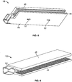
Figure 1 is an embodiment which is not according to the present invention but was included in the application as originally filed. -
Figure 2 is an internal view of the components in an input module which is not according to the present invention but was included in the application as originally filed. -
Figure 3 is a top view of the input module ofFigure 2 . -
Figure 4 is an output module which is not according to the present invention but was included in the application as originally filed. -
Figure 5 is an internal view of the output module ofFigure 4 . -
Figure 6 is an embodiment of the present invention. -
Figure 7 is a top view of the present invention without covers. -
Figures 8-11 provide alternate views of the present invention. -
Figure 12 is a perspective view of an embodiment of the present invention. -
Figures 13-14 provide alternate view of the present invention. -
Figure 15 is a perspective view of an embodiment of the present invention. - The present invention is directed to a PV box that connects to the edge of the PV array. One advantage of the present invention is the unique edge placement location of the connector on the array.
Figure 1 shows an embodiment of theedge connector 10, which includes anoutput plug 12 and aninput module 14. Theoutput plug 12 andinput module 14 interconnect with acable 70 and plug 72 connection. In a PV system, thearrays output plug 12 is secured to thefirst array 16. Theinput module 14 is secured to the nextadjacent array 18. Eacharray output plug 12, oneinput module 14, and acable 70 andplug connection 72 attached. -
Figure 2 illustrates the components of theedge connector 10. In theoutput plug 12, ablade 20 is used to mate with the conductive foil (not shown) of the array and conduct the photon energy from the array to theedge connector 10. A diode 22 (See e.g.Figure 15 ) is connected to the power circuit to ensure proper conduction of the energy, and a heat sink 24 (See e.g.Figure 15 ) is disposed on thediode 22 to act as an electrical contact and heat dissipater. While any suitable diode may be used, a TO-220 Schottky diode may be used with this embodiment, and while any suitable heat sink may be used, a copper iron sink may be used with this embodiment. Acomponent shuttle 26 is used to manage thecomponents edge connector 10 during manufacture and maintain proper placement of thecomponents shuttle 26, arivet 28 is used to secure theheat sink 24 to the diode. In alternative to therivet 28, a solder or resistance weld connection may be used (not shown), such as an ultra sonic weld connection. Thehousing 30 is overmolded on the components and has a 'U'shaped channel 48 to accommodate the array. Thearray plates channel 48 of theedge connector 10. In one embodiment, Room Temperature Vulcanization (RTV) silicon is used as the epoxy to maintain a secure and waterproof hold of theconnector 10 on thearray connector 10 to thearrays - Referring to
Figure 3 ,apertures 34 are located on the top surface of thehousing 30 to provide receptacles for a soldering connection with the array foils. Once the conductive connection to thearray apertures 34 are sealed and filled in with silicon or other suitable sealing and protective material. -
Figures 4 and5 show theinput module 14 of the edge connector. A crimp connection is disposed on the inside of themodule 14. The housing 40 has afoil access window 42, which permits a conductive connection to be made from the array (not shown inFigures 4 and5 ) to themodule 14. Thewindow 42 is filled in or covered for protection. - An embodiment, shown in
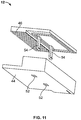
Figures 6-11 , of the output module (not shown) of theedge connector 10 includes a two-piece design, having ahousing portion 44 and acover portion 46. When placed on thehousing portion 44, thecover portion 46 andhousing portion 44 define achannel 48. Thearrays channel 48 and a connection is made between theconnector 10 and the array foils 14, 16.Figure 7 illustrates theedge connector 10 with the cover portion removed. Agroove 50 is molded in thehousing 44 to help contain sealant and to align thecover portion 46 when in place. Thehousing portion 44 also haslarge latch receptacles 52 that accept thelatches 54 on the cover portion 46 (Figures 8-11 ) when thecover portion 46 is in place. -
Figures 8-11 illustrate various views of the two-piece edge connector. The inner surface of thechannel 48 is ridged or ribbed to provide an enhanced surface for bonding onto the array. Once theconnector 10 is placed onto thearray connector 10 to the array with a waterproof bond. Thecover portion 46 haslatches 54 to hold thecover portion 46 on thehousing portion 44 when in place. The exemplary embodiment has twolatches 54, however, any number of latches may be used. Thehousing portion 44 haslatch receptacles 52 that are designed to accept thelatches 54 when in place. Once thecover portion 46 is placed on thehousing portion 44, thelatches 54 are engaged in thereceptacles 52 and are not easily removable. - Yet another embodiment of the input module of the present invention includes a two-piece design where the
cover portion 46 is designed to allow for a thicker array edge shown inFigure 12 .Arrays edge connectors 10 must be designed to accommodate a range of thicknesses e.g. 6.4 mm to 19.1 mm (¼ inch to ¾ inch).Figure 12 illustrates acover portion 46 that is two tiered. Thefirst tier 60 rests on thehousing portion 44 and thesecond tier 62 forms a portion of thechannel 48 that fits around the array edge. Thehousing portion 44 has agroove 50 to contain sealant when applied to secure theconnector 10 to the array and to secure thecover portion 46 to thehousing portion 44. -
Figures 13-15 illustrate another embodiment of the present invention. The edge connector (not shown inFigures 13-15 ) is a two-piece design with acover portion 46 and ahousing portion 44 where thechannel 48 is formed to fit onto anarray cover portion 46 has a two-tiered shape, with afirst tier 60 and asecond tier 62. Thecover portion 46 hasapertures 66 that acceptfasteners 68, e.g. screws, and secure thecover portion 46 to thehousing portion 44. The height of thechannel 48 may vary, depending on the thickness of the array. - The
cover portion 46 fits onto the top of thehousing portion 44 and is secured withfasters 68. Adiode 22 is connected to the circuitry to ensure proper conduction of the energy, and aheat sink 24 is placed in contact with thediode 22 to act as a contact and heat dissipater. Acomponent shuttle 26 is used to manage the components of theedge connector 10 during manufacture. Theshuttle 26 holds the components in place. In addition to theshuttle 26, arivet 28 is used to secure theheat sink 24 to the diode. An alternative to therivet 28, a solder or weld connection may be used, such as an ultra sonic weld connection. A connector is used to mate with an adjacent edge connector (not shown) to transmit the energy from the array. - The
edge connector 10 may be of an size or dimensions suitable for the array, however, the dimensions may be 101.6 mm (4 inches) in length, 25.4 mm (1 inch) deep, and 9.5 mm to 22.2 mm (3/8 inch to 7/8 inch) thick. Typically, the array is 6.4 mm to 25.4 mm (¼ inch to 1 inch) thick, therefore, thechannel 48 on theconnector 10 be at least wide enough to accommodate the array of this thickness to fit snugly into thechannel 48. - Preferably, the connector operates with at least 15 amps of current, however the
connector 10 accommodates a minimum of 0.5 amps to a maximum of 18 amps with the TO-220 diode. The connector may also be connected in series to a maximum of thirty connectors, where themale connection 72a of one connector mates with thefemale connection 72b of the adjacent connector. Theedge connector 10 may also include larger heat sinks, to allow for a larger current capacity. A larger heat sink provides greater heat dissipation, and requires a correspondinglylarger connector 10 housing.
Claims (8)
- An electrical connector (10) for interconnecting adjacent photovoltaic arrays (16, 18) along an edge, the connector (10) comprising:(a) an input module (12) having an input module housing unit (30) having:at least one diode (22) to support a predetermined voltage and current;at least one heat sink (24) in thermal communication with the diode (22) and configured to dissipate heat;at least two connection points (20) being electrically conductive;a U-shaped channel (48) configured to receive the edge of a first photovoltaic array (16);a base portion (26, 44) configured to hold the at least one diode (22), the heat sink (24), the connection points (20), and the channel (48);a cover portion (46) wherein the cover portion (46) and the base portion (26,44) are secured with a fastener (54, 68) to define the U-shaped channel (48);(b) an output module (14) configured to connect with the input module (12), the output module (12) having:at least two connection points (20) being electrically conductive;a U-shaped channel (48) configured to receive the edge of a second photovoltaic array (18);a base portion (26, 44) configured to hold the connection points (20) and the channel (48); and(c) an electrically conductive cable (70) connecting the input module (12) and output module (14);
wherein the input module (12) and the output module (14) are secured to the edges of photovoltaic arrays (16, 18) and are in electrical communication with each other through the electrically conductive cable (70) and wherein the connection points (20) conduct electrical energy from the arrays (16, 18) to the connector (10). - The connector (10) of claim 1 wherein the diode (22) is a TO-220 Schottky diode.
- The connector (10) of claim 1 wherein the heat sink (24) is secured to the base portion (26) with an ultra sonic weld connection, resistance weld connection or rivet (28).
- The connector (10) of claim 1 wherein the diode (22) and the heat sink (24) are a unitary device.
- The connector (10) of claim 1 wherein the input module (12) and the output module (14) are secured to the photovoltaic arrays (16, 18) with a silicon epoxy.
- The connector (10) of claim 1 wherein the predetermined current is a minimum of 0.5 amps and the predetermined current is a maximum of 18 amps.
- The connector (10) of claim 1 further comprising a male connection (72a) and a female connection (72b), wherein a plurality of connectors are connected to photovoltaic arrays in series and the male connection (72a) of a first connector mates with the female connection (72b) of an adjacent connector.
- The connector (10) of claim 7 wherein a maximum of thirty connectors are connected in series.
Applications Claiming Priority (2)
| Application Number | Priority Date | Filing Date | Title |
|---|---|---|---|
| US11/930,331 US7625238B2 (en) | 2007-10-31 | 2007-10-31 | Low profile photovoltaic edge connector |
| PCT/US2008/012163 WO2009058231A1 (en) | 2007-10-31 | 2008-10-27 | Low profile photovoltaic edge connector |
Publications (2)
| Publication Number | Publication Date |
|---|---|
| EP2179452A1 EP2179452A1 (en) | 2010-04-28 |
| EP2179452B1 true EP2179452B1 (en) | 2017-07-26 |
Family
ID=40456930
Family Applications (1)
| Application Number | Title | Priority Date | Filing Date |
|---|---|---|---|
| EP08843566.4A Active EP2179452B1 (en) | 2007-10-31 | 2008-10-27 | Low profile photovoltaic edge connector |
Country Status (4)
| Country | Link |
|---|---|
| US (1) | US7625238B2 (en) |
| EP (1) | EP2179452B1 (en) |
| CN (1) | CN101842913B (en) |
| WO (1) | WO2009058231A1 (en) |
Families Citing this family (19)
| Publication number | Priority date | Publication date | Assignee | Title |
|---|---|---|---|---|
| US7713089B2 (en) * | 2008-02-22 | 2010-05-11 | Redwood Renewable, Llc | Photovoltaic roofing tile with a plug and socket on 2 opposite edges |
| US8435056B2 (en) * | 2009-04-16 | 2013-05-07 | Enphase Energy, Inc. | Apparatus for coupling power generated by a photovoltaic module to an output |
| WO2011064820A1 (en) * | 2009-11-27 | 2011-06-03 | オーナンバ株式会社 | Solar cell module |
| CN102347577B (en) * | 2010-07-27 | 2013-07-17 | 泰科电子(上海)有限公司 | Electric connection system and frame with same |
| US9083121B2 (en) * | 2010-12-17 | 2015-07-14 | Sunpower Corporation | Diode-included connector, photovoltaic laminate and photovoltaic assembly using same |
| DE102010056591A1 (en) * | 2010-12-30 | 2012-07-05 | Masdar Pv Gmbh | Photovoltaic module for use in solar system that is attached to e.g. roof, has connection devices for electrically contacting cells and for enclosing edge section of carrier for electrically contacting and mechanically holding module |
| CN103477445A (en) | 2011-03-22 | 2013-12-25 | 陶氏环球技术有限责任公司 | Improved photovoltaic sheathing element with a flexible connector assembly |
| CN103828228A (en) | 2011-07-18 | 2014-05-28 | 恩菲斯能源公司 | Resilient mounting assembly for photovoltaic modules |
| CN102376806B (en) * | 2011-10-21 | 2012-11-21 | 常熟市冠日新材料有限公司 | Junction box capable of being arranged at side face of solar energy photovoltaic module |
| USD745846S1 (en) | 2012-03-01 | 2015-12-22 | Ilsco Corporation | Solar panel electrical connector |
| DE102012011346A1 (en) * | 2012-06-11 | 2013-12-12 | Carl Freudenberg Kg | solar module |
| USD734653S1 (en) | 2012-11-09 | 2015-07-21 | Enphase Energy, Inc. | AC module mounting bracket |
| US10432132B2 (en) | 2013-07-01 | 2019-10-01 | RBI Solar, Inc. | Solar mounting system having automatic grounding and associated methods |
| JP2017524326A (en) * | 2014-07-25 | 2017-08-24 | マルチ−ホールディング アーゲー | Junction box for solar cell module |
| US10756669B2 (en) | 2014-12-04 | 2020-08-25 | Solarmass Energy Group Ltd. | Solar roof tile |
| US11056997B2 (en) | 2015-06-27 | 2021-07-06 | Sunpower Corporation | Universal photovoltaic laminate |
| US10693413B2 (en) * | 2017-10-19 | 2020-06-23 | Building Materials Investment Corporation | Roof integrated photovoltaic system |
| EP3503384B1 (en) * | 2017-12-20 | 2021-09-15 | Lapp Engineering AG | Connection device, electric module and connection method |
| US10530292B1 (en) | 2019-04-02 | 2020-01-07 | Solarmass Energy Group Ltd. | Solar roof tile with integrated cable management system |
Family Cites Families (8)
| Publication number | Priority date | Publication date | Assignee | Title |
|---|---|---|---|---|
| US4990099A (en) * | 1989-09-18 | 1991-02-05 | High Voltage Engineering Corp. | Keyed electrical connector with main and auxiliary electrical contacts |
| JP3605032B2 (en) * | 2000-06-07 | 2004-12-22 | 三洋電機株式会社 | Solar cell module, solar cell module connection method, solar cell module installation method, and solar cell module ground connection method |
| JP4087106B2 (en) | 2001-11-22 | 2008-05-21 | 積水樹脂株式会社 | Method for manufacturing solar cell panel and terminal box for solar cell module |
| DE20311183U1 (en) * | 2003-07-21 | 2004-07-08 | Tyco Electronics Amp Gmbh | Junction box for a solar panel and solar panel |
| JP4401915B2 (en) * | 2004-09-21 | 2010-01-20 | 矢崎総業株式会社 | Connector with liquid intrusion prevention structure |
| DE102005020129A1 (en) * | 2005-04-29 | 2006-11-09 | Tyco Electronics Amp Gmbh | Solar module for generating electrical energy |
| DE102005022226B4 (en) | 2005-05-10 | 2008-05-15 | RUNGE, André | Cooling arrangement for arranged in a housing electronic components |
| US7387537B1 (en) * | 2007-01-03 | 2008-06-17 | Tyco Electronics Corporation | Connector system for solar cell roofing tiles |
-
2007
- 2007-10-31 US US11/930,331 patent/US7625238B2/en active Active
-
2008
- 2008-10-27 CN CN2008801141298A patent/CN101842913B/en active Active
- 2008-10-27 WO PCT/US2008/012163 patent/WO2009058231A1/en not_active Ceased
- 2008-10-27 EP EP08843566.4A patent/EP2179452B1/en active Active
Non-Patent Citations (1)
| Title |
|---|
| None * |
Also Published As
| Publication number | Publication date |
|---|---|
| US20090142945A1 (en) | 2009-06-04 |
| CN101842913A (en) | 2010-09-22 |
| CN101842913B (en) | 2012-09-05 |
| WO2009058231A1 (en) | 2009-05-07 |
| EP2179452A1 (en) | 2010-04-28 |
| US7625238B2 (en) | 2009-12-01 |
Similar Documents
| Publication | Publication Date | Title |
|---|---|---|
| US7625238B2 (en) | Low profile photovoltaic edge connector | |
| US8222533B2 (en) | Low profile photovoltaic (LPPV) box | |
| US7291036B1 (en) | Photovoltaic connection system | |
| US20080253092A1 (en) | Heat Dissipation System for Photovoltaic Interconnection System | |
| US20080110490A1 (en) | Photovoltaic connection system | |
| US20080135092A1 (en) | Solar roof tiles with heat exchange | |
| KR101611638B1 (en) | Photovoltaic module kit including connector assembly for non-penetrating array installation | |
| US9412890B1 (en) | Photovoltaic module pin electrical connectors | |
| AU2007333183A1 (en) | Solar roof tiles and modules with heat exchange | |
| US20100105238A1 (en) | Solar laminate connector | |
| US20120222718A1 (en) | Photovoltaic grounding & bonding connector | |
| US20110308566A1 (en) | Photovoltaic module and the way of connecting photovoltaic modules in a photovoltaic system | |
| US20120152325A1 (en) | Junction box attachment to solar module laminate | |
| KR100996242B1 (en) | Solar ac power generation device | |
| US20130169056A1 (en) | Multi-module inverters and converters for building integrable photovoltaic modules | |
| US10284104B2 (en) | Integral inverter and solar cell module including the same | |
| US20140182651A1 (en) | Integrated junction insulation for photovoltaic module | |
| US20140305494A1 (en) | Header structures for flexible photovoltaic modules | |
| CN102792460B (en) | Solar module | |
| US20130180575A1 (en) | Structures for Solar Roofing | |
| CN216794887U (en) | Solar power generation element array | |
| KR20140042832A (en) | Concentrating photovoltaic module panel improving stiffness and assembly of baseplate | |
| KR101506705B1 (en) | inverter integrated sollar cell pannel | |
| CN107820675A (en) | Terminals for solar junction boxes | |
| KR20150140019A (en) | Double-sided light receiving solar power generation device |
Legal Events
| Date | Code | Title | Description |
|---|---|---|---|
| PUAI | Public reference made under article 153(3) epc to a published international application that has entered the european phase |
Free format text: ORIGINAL CODE: 0009012 |
|
| 17P | Request for examination filed |
Effective date: 20100310 |
|
| AK | Designated contracting states |
Kind code of ref document: A1 Designated state(s): AT BE BG CH CY CZ DE DK EE ES FI FR GB GR HR HU IE IS IT LI LT LU LV MC MT NL NO PL PT RO SE SI SK TR |
|
| AX | Request for extension of the european patent |
Extension state: AL BA MK RS |
|
| DAX | Request for extension of the european patent (deleted) | ||
| 17Q | First examination report despatched |
Effective date: 20140625 |
|
| REG | Reference to a national code |
Ref country code: DE Ref legal event code: R079 Ref document number: 602008051328 Country of ref document: DE Free format text: PREVIOUS MAIN CLASS: H01L0031050000 Ipc: H02S0040340000 |
|
| RAP1 | Party data changed (applicant data changed or rights of an application transferred) |
Owner name: TE CONNECTIVITY CORPORATION |
|
| GRAP | Despatch of communication of intention to grant a patent |
Free format text: ORIGINAL CODE: EPIDOSNIGR1 |
|
| RIC1 | Information provided on ipc code assigned before grant |
Ipc: H02S 40/34 20140101AFI20170202BHEP |
|
| INTG | Intention to grant announced |
Effective date: 20170302 |
|
| GRAS | Grant fee paid |
Free format text: ORIGINAL CODE: EPIDOSNIGR3 |
|
| GRAA | (expected) grant |
Free format text: ORIGINAL CODE: 0009210 |
|
| AK | Designated contracting states |
Kind code of ref document: B1 Designated state(s): AT BE BG CH CY CZ DE DK EE ES FI FR GB GR HR HU IE IS IT LI LT LU LV MC MT NL NO PL PT RO SE SI SK TR |
|
| REG | Reference to a national code |
Ref country code: GB Ref legal event code: FG4D |
|
| REG | Reference to a national code |
Ref country code: CH Ref legal event code: EP |
|
| REG | Reference to a national code |
Ref country code: AT Ref legal event code: REF Ref document number: 913157 Country of ref document: AT Kind code of ref document: T Effective date: 20170815 |
|
| REG | Reference to a national code |
Ref country code: IE Ref legal event code: FG4D |
|
| REG | Reference to a national code |
Ref country code: DE Ref legal event code: R096 Ref document number: 602008051328 Country of ref document: DE |
|
| REG | Reference to a national code |
Ref country code: FR Ref legal event code: PLFP Year of fee payment: 10 |
|
| REG | Reference to a national code |
Ref country code: NL Ref legal event code: MP Effective date: 20170726 |
|
| REG | Reference to a national code |
Ref country code: LT Ref legal event code: MG4D |
|
| REG | Reference to a national code |
Ref country code: AT Ref legal event code: MK05 Ref document number: 913157 Country of ref document: AT Kind code of ref document: T Effective date: 20170726 |
|
| PG25 | Lapsed in a contracting state [announced via postgrant information from national office to epo] |
Ref country code: FI Free format text: LAPSE BECAUSE OF FAILURE TO SUBMIT A TRANSLATION OF THE DESCRIPTION OR TO PAY THE FEE WITHIN THE PRESCRIBED TIME-LIMIT Effective date: 20170726 Ref country code: AT Free format text: LAPSE BECAUSE OF FAILURE TO SUBMIT A TRANSLATION OF THE DESCRIPTION OR TO PAY THE FEE WITHIN THE PRESCRIBED TIME-LIMIT Effective date: 20170726 Ref country code: NO Free format text: LAPSE BECAUSE OF FAILURE TO SUBMIT A TRANSLATION OF THE DESCRIPTION OR TO PAY THE FEE WITHIN THE PRESCRIBED TIME-LIMIT Effective date: 20171026 Ref country code: NL Free format text: LAPSE BECAUSE OF FAILURE TO SUBMIT A TRANSLATION OF THE DESCRIPTION OR TO PAY THE FEE WITHIN THE PRESCRIBED TIME-LIMIT Effective date: 20170726 Ref country code: HR Free format text: LAPSE BECAUSE OF FAILURE TO SUBMIT A TRANSLATION OF THE DESCRIPTION OR TO PAY THE FEE WITHIN THE PRESCRIBED TIME-LIMIT Effective date: 20170726 Ref country code: SE Free format text: LAPSE BECAUSE OF FAILURE TO SUBMIT A TRANSLATION OF THE DESCRIPTION OR TO PAY THE FEE WITHIN THE PRESCRIBED TIME-LIMIT Effective date: 20170726 Ref country code: LT Free format text: LAPSE BECAUSE OF FAILURE TO SUBMIT A TRANSLATION OF THE DESCRIPTION OR TO PAY THE FEE WITHIN THE PRESCRIBED TIME-LIMIT Effective date: 20170726 |
|
| PG25 | Lapsed in a contracting state [announced via postgrant information from national office to epo] |
Ref country code: GR Free format text: LAPSE BECAUSE OF FAILURE TO SUBMIT A TRANSLATION OF THE DESCRIPTION OR TO PAY THE FEE WITHIN THE PRESCRIBED TIME-LIMIT Effective date: 20171027 Ref country code: PL Free format text: LAPSE BECAUSE OF FAILURE TO SUBMIT A TRANSLATION OF THE DESCRIPTION OR TO PAY THE FEE WITHIN THE PRESCRIBED TIME-LIMIT Effective date: 20170726 Ref country code: IS Free format text: LAPSE BECAUSE OF FAILURE TO SUBMIT A TRANSLATION OF THE DESCRIPTION OR TO PAY THE FEE WITHIN THE PRESCRIBED TIME-LIMIT Effective date: 20171126 Ref country code: BG Free format text: LAPSE BECAUSE OF FAILURE TO SUBMIT A TRANSLATION OF THE DESCRIPTION OR TO PAY THE FEE WITHIN THE PRESCRIBED TIME-LIMIT Effective date: 20171026 Ref country code: LV Free format text: LAPSE BECAUSE OF FAILURE TO SUBMIT A TRANSLATION OF THE DESCRIPTION OR TO PAY THE FEE WITHIN THE PRESCRIBED TIME-LIMIT Effective date: 20170726 |
|
| PG25 | Lapsed in a contracting state [announced via postgrant information from national office to epo] |
Ref country code: DK Free format text: LAPSE BECAUSE OF FAILURE TO SUBMIT A TRANSLATION OF THE DESCRIPTION OR TO PAY THE FEE WITHIN THE PRESCRIBED TIME-LIMIT Effective date: 20170726 Ref country code: RO Free format text: LAPSE BECAUSE OF FAILURE TO SUBMIT A TRANSLATION OF THE DESCRIPTION OR TO PAY THE FEE WITHIN THE PRESCRIBED TIME-LIMIT Effective date: 20170726 Ref country code: CZ Free format text: LAPSE BECAUSE OF FAILURE TO SUBMIT A TRANSLATION OF THE DESCRIPTION OR TO PAY THE FEE WITHIN THE PRESCRIBED TIME-LIMIT Effective date: 20170726 |
|
| REG | Reference to a national code |
Ref country code: DE Ref legal event code: R097 Ref document number: 602008051328 Country of ref document: DE |
|
| PG25 | Lapsed in a contracting state [announced via postgrant information from national office to epo] |
Ref country code: EE Free format text: LAPSE BECAUSE OF FAILURE TO SUBMIT A TRANSLATION OF THE DESCRIPTION OR TO PAY THE FEE WITHIN THE PRESCRIBED TIME-LIMIT Effective date: 20170726 Ref country code: MC Free format text: LAPSE BECAUSE OF FAILURE TO SUBMIT A TRANSLATION OF THE DESCRIPTION OR TO PAY THE FEE WITHIN THE PRESCRIBED TIME-LIMIT Effective date: 20170726 Ref country code: IT Free format text: LAPSE BECAUSE OF FAILURE TO SUBMIT A TRANSLATION OF THE DESCRIPTION OR TO PAY THE FEE WITHIN THE PRESCRIBED TIME-LIMIT Effective date: 20170726 Ref country code: SK Free format text: LAPSE BECAUSE OF FAILURE TO SUBMIT A TRANSLATION OF THE DESCRIPTION OR TO PAY THE FEE WITHIN THE PRESCRIBED TIME-LIMIT Effective date: 20170726 |
|
| REG | Reference to a national code |
Ref country code: CH Ref legal event code: PL |
|
| PLBE | No opposition filed within time limit |
Free format text: ORIGINAL CODE: 0009261 |
|
| STAA | Information on the status of an ep patent application or granted ep patent |
Free format text: STATUS: NO OPPOSITION FILED WITHIN TIME LIMIT |
|
| 26N | No opposition filed |
Effective date: 20180430 |
|
| REG | Reference to a national code |
Ref country code: IE Ref legal event code: MM4A |
|
| PG25 | Lapsed in a contracting state [announced via postgrant information from national office to epo] |
Ref country code: LU Free format text: LAPSE BECAUSE OF NON-PAYMENT OF DUE FEES Effective date: 20171027 Ref country code: CH Free format text: LAPSE BECAUSE OF NON-PAYMENT OF DUE FEES Effective date: 20171031 Ref country code: LI Free format text: LAPSE BECAUSE OF NON-PAYMENT OF DUE FEES Effective date: 20171031 |
|
| REG | Reference to a national code |
Ref country code: BE Ref legal event code: MM Effective date: 20171031 |
|
| PG25 | Lapsed in a contracting state [announced via postgrant information from national office to epo] |
Ref country code: BE Free format text: LAPSE BECAUSE OF NON-PAYMENT OF DUE FEES Effective date: 20171031 Ref country code: SI Free format text: LAPSE BECAUSE OF FAILURE TO SUBMIT A TRANSLATION OF THE DESCRIPTION OR TO PAY THE FEE WITHIN THE PRESCRIBED TIME-LIMIT Effective date: 20170726 |
|
| REG | Reference to a national code |
Ref country code: FR Ref legal event code: PLFP Year of fee payment: 11 |
|
| PG25 | Lapsed in a contracting state [announced via postgrant information from national office to epo] |
Ref country code: MT Free format text: LAPSE BECAUSE OF NON-PAYMENT OF DUE FEES Effective date: 20171027 |
|
| PG25 | Lapsed in a contracting state [announced via postgrant information from national office to epo] |
Ref country code: IE Free format text: LAPSE BECAUSE OF NON-PAYMENT OF DUE FEES Effective date: 20171027 |
|
| PG25 | Lapsed in a contracting state [announced via postgrant information from national office to epo] |
Ref country code: HU Free format text: LAPSE BECAUSE OF FAILURE TO SUBMIT A TRANSLATION OF THE DESCRIPTION OR TO PAY THE FEE WITHIN THE PRESCRIBED TIME-LIMIT; INVALID AB INITIO Effective date: 20081027 |
|
| PG25 | Lapsed in a contracting state [announced via postgrant information from national office to epo] |
Ref country code: ES Free format text: LAPSE BECAUSE OF NON-PAYMENT OF DUE FEES Effective date: 20170726 |
|
| PG25 | Lapsed in a contracting state [announced via postgrant information from national office to epo] |
Ref country code: CY Free format text: LAPSE BECAUSE OF NON-PAYMENT OF DUE FEES Effective date: 20170726 |
|
| PG25 | Lapsed in a contracting state [announced via postgrant information from national office to epo] |
Ref country code: TR Free format text: LAPSE BECAUSE OF FAILURE TO SUBMIT A TRANSLATION OF THE DESCRIPTION OR TO PAY THE FEE WITHIN THE PRESCRIBED TIME-LIMIT Effective date: 20170726 |
|
| PG25 | Lapsed in a contracting state [announced via postgrant information from national office to epo] |
Ref country code: PT Free format text: LAPSE BECAUSE OF FAILURE TO SUBMIT A TRANSLATION OF THE DESCRIPTION OR TO PAY THE FEE WITHIN THE PRESCRIBED TIME-LIMIT Effective date: 20170726 |
|
| PGFP | Annual fee paid to national office [announced via postgrant information from national office to epo] |
Ref country code: FR Payment date: 20210913 Year of fee payment: 14 |
|
| PGFP | Annual fee paid to national office [announced via postgrant information from national office to epo] |
Ref country code: GB Payment date: 20210915 Year of fee payment: 14 |
|
| GBPC | Gb: european patent ceased through non-payment of renewal fee |
Effective date: 20221027 |
|
| PG25 | Lapsed in a contracting state [announced via postgrant information from national office to epo] |
Ref country code: FR Free format text: LAPSE BECAUSE OF NON-PAYMENT OF DUE FEES Effective date: 20221031 |
|
| PG25 | Lapsed in a contracting state [announced via postgrant information from national office to epo] |
Ref country code: GB Free format text: LAPSE BECAUSE OF NON-PAYMENT OF DUE FEES Effective date: 20221027 |
|
| PGFP | Annual fee paid to national office [announced via postgrant information from national office to epo] |
Ref country code: DE Payment date: 20250902 Year of fee payment: 18 |