EP2178208A2 - Systems and methods to overcome DC offsets in amplifiers used to start resonant micro-electro mechanical systems - Google Patents
Systems and methods to overcome DC offsets in amplifiers used to start resonant micro-electro mechanical systems Download PDFInfo
- Publication number
- EP2178208A2 EP2178208A2 EP09172605A EP09172605A EP2178208A2 EP 2178208 A2 EP2178208 A2 EP 2178208A2 EP 09172605 A EP09172605 A EP 09172605A EP 09172605 A EP09172605 A EP 09172605A EP 2178208 A2 EP2178208 A2 EP 2178208A2
- Authority
- EP
- European Patent Office
- Prior art keywords
- signal
- gain
- resonating
- circuit
- drive
- Prior art date
- Legal status (The legal status is an assumption and is not a legal conclusion. Google has not performed a legal analysis and makes no representation as to the accuracy of the status listed.)
- Withdrawn
Links
- 238000000034 method Methods 0.000 title claims abstract description 8
- 230000000977 initiatory effect Effects 0.000 abstract description 2
- 239000003990 capacitor Substances 0.000 description 4
- 238000006073 displacement reaction Methods 0.000 description 2
- 238000010586 diagram Methods 0.000 description 1
- 230000001052 transient effect Effects 0.000 description 1
Images

Classifications
-
- H—ELECTRICITY
- H03—ELECTRONIC CIRCUITRY
- H03H—IMPEDANCE NETWORKS, e.g. RESONANT CIRCUITS; RESONATORS
- H03H9/00—Networks comprising electromechanical or electro-acoustic elements; Electromechanical resonators
- H03H9/02—Details
- H03H9/02244—Details of microelectro-mechanical resonators
- H03H9/02393—Post-fabrication trimming of parameters, e.g. resonance frequency, Q factor
- H03H9/02409—Post-fabrication trimming of parameters, e.g. resonance frequency, Q factor by application of a DC-bias voltage
-
- G—PHYSICS
- G01—MEASURING; TESTING
- G01C—MEASURING DISTANCES, LEVELS OR BEARINGS; SURVEYING; NAVIGATION; GYROSCOPIC INSTRUMENTS; PHOTOGRAMMETRY OR VIDEOGRAMMETRY
- G01C19/00—Gyroscopes; Turn-sensitive devices using vibrating masses; Turn-sensitive devices without moving masses; Measuring angular rate using gyroscopic effects
- G01C19/56—Turn-sensitive devices using vibrating masses, e.g. vibratory angular rate sensors based on Coriolis forces
- G01C19/5776—Signal processing not specific to any of the devices covered by groups G01C19/5607 - G01C19/5719
-
- H—ELECTRICITY
- H03—ELECTRONIC CIRCUITRY
- H03F—AMPLIFIERS
- H03F3/00—Amplifiers with only discharge tubes or only semiconductor devices as amplifying elements
- H03F3/70—Charge amplifiers
-
- H—ELECTRICITY
- H03—ELECTRONIC CIRCUITRY
- H03K—PULSE TECHNIQUE
- H03K5/00—Manipulating of pulses not covered by one of the other main groups of this subclass
- H03K5/003—Changing the DC level
-
- H—ELECTRICITY
- H03—ELECTRONIC CIRCUITRY
- H03F—AMPLIFIERS
- H03F2200/00—Indexing scheme relating to amplifiers
- H03F2200/375—Circuitry to compensate the offset being present in an amplifier
Definitions
- Start up of the MEMS gyro is performed by amplifying electronics noise, which goes into a comparator which then drives logic that generates a drive waveform.
- the input of the initial drive stage often includes electrostatic discharge (ESD) protection, such as an ESD diode.
- ESD electrostatic discharge
- the ESD protection can often introduce a leakage current, which leads to a DC offset. If that DC offset is too large, a comparator in the initial drive stage never switches (no clock signal is sent to a drive component), no drive signal is generated, and the sensor never starts.
- ASIC application specific integrated circuit
- the present invention provides systems and methods for insuring successful initiation of a resonating micro-electro mechanical systems (MEMS).
- An example system includes a resonating sensor, a drive device, a variable gain charge amplifier, and a variable gain voltage amplifier.
- the charge amplifier receives signals from the resonating sensor, compensates this signal for a DC offset, and generates a clock signal for the drive device, thus placing the resonating sensor in a steady state operating mode.
- the circuit includes a plurality of gain switches being controllable for adjusting gain of the circuit.
- the circuit includes a comparator that generates the clock signal for the drive device if a signal associated with the received signal exceeds a reference signal. Toggling of the gain switches produces a glitch in the signal associated with the received signal, which in turn causes the comparator to switch. The zero crossing of the comparator causes a cycle of the drive to be generated. The drive adds energy to the resonator. The displacement of the resonator becomes visible at the output of the charge amplifier and overcomes the DC offset.
- the controller toggles one or more of the gain switches at a predefined frequency.
- the predefined frequency corresponds to a desired resonance of the sensor.
- FIGURE 1 illustrates a block diagram of an example system formed in accordance with the present invention.
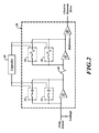
- FIGURE 2 illustrates components of the charge amplifier and voltage gain circuit of FIGURE 2 .
- FIGURE 1 illustrates a resonating micro-electro mechanical systems (MEMS) device 20 that overcomes a DC offset introduced by electrostatic discharge (ESD) components (e.g., diode), thereby avoiding a situation where the MEMS device 20 fails to start.
- MEMS micro-electro mechanical systems
- the MEMS device 20 includes one or more sensors 24, a drive generator 26, a charge amp, gain circuit 28, and a controller 30.
- the drive generator 26 and the charge amp and voltage gain circuit 28 are in signal communication with the sensors 24 (e.g. resonating proof mass or double-ended tuning fork).
- the controller 30 is in signal communication with components of the gain circuit 28.
- the controller 30 causes the charge amplifier and voltage gain circuit 28 to produce a spiked signal that is large enough to overcome any experienced DC offset, thereby allowing the gain circuit 28 to output a clock signal for the drive generator 26.
- FIGURE 2 illustrates an example configuration of the charge amplifier and voltage gain circuit 28.
- the circuit 28 includes a first charge amplifier 52 (op-amp with feedback capacitor) that receives an ESD protected signal from the resonating MEMS device 20 with switch/capacitor pairs 32, 34 connected in parallel between the input and output terminals. In normal operation, different capacitance values can be selected for different charge amplifier gains.
- a resistor 40 is located between the output of the first amplifier 52 and an input to a second amplifier 42 (inverting amplifier). Multiple switch/resistor pairs 44, 46 are connected in parallel between the input and an output terminal of the second amplifier 42.
- the output terminal of the second amplifier 42 is connected to an input of a comparator 50.
- the comparator 50 compares the input signal to a reference signal that is also a reference signal for the first and second amplifiers 52, 42.
- the switches in the switch pairs 32, 34, 44, 46 are connected to a controller 30.
- the controller 30 toggles one of the switches in the switch pairs 32, 34, 44, 46. This introduces a transient signal or glitch in the signal path at the input to the comparator 50. If the glitch produced is bigger than the DC offset (caused by voltage leakage introduced by ESD protection components), the comparator 50 will trip, generate a clock, a motor drive, and permit start-up of the resonator.
- the gains are changed rapidly (at or near a desired drive/motor frequency of the drive generator 26), a drive signal will be generated at the corresponding frequency. Therefore, the DC offset is overcome by rapidly switching the gains (the switches) until the actual resonator displacement has built up enough to overcome the DC offset.
- the controller 30 is a hardware and/or software system that rapidly switches the gains (ideally at the resonator frequency) until the resonator amplitude has built up. Then, the device 20 continues running with the steady state gains.
- only one spike of the signal seen by the comparator 50 may be enough to allow the system to start.
- the size of the capacitors and resistors used in the switch/capacitor and switch/resistor pairs 32, 34, 44, 46 may vary depending upon desired gains across the respective amplifier.
Landscapes
- Physics & Mathematics (AREA)
- Engineering & Computer Science (AREA)
- Nonlinear Science (AREA)
- Signal Processing (AREA)
- General Physics & Mathematics (AREA)
- Radar, Positioning & Navigation (AREA)
- Remote Sensing (AREA)
- Power Engineering (AREA)
- Acoustics & Sound (AREA)
- Gyroscopes (AREA)
- Micromachines (AREA)
- Oscillators With Electromechanical Resonators (AREA)
Abstract
Systems and methods for insuring successful initiation of a resonating micro-electro mechanical systems (MEMS). An example system (20) includes a resonating sensor (24), a drive device (26), a charge amplifier, and a voltage gain circuit (28). At start up, the charge amplifier and voltage gain circuit receives signals from the resonating sensor, compensates this signal for DC offsets, and generates a clock signal for the drive, thus placing the resonating sensor in a steady state operating mode. The circuit includes a plurality of switches that are toggled to produce a glitch in the signal associated with the received signal. The glitch overcomes the DC offset. A comparator generates the clock signal for the drive device if a signal associated with the received signal exceeds a reference signal.
Description
- Start up of the MEMS gyro is performed by amplifying electronics noise, which goes into a comparator which then drives logic that generates a drive waveform. The input of the initial drive stage (charge amplifier) often includes electrostatic discharge (ESD) protection, such as an ESD diode. The ESD protection can often introduce a leakage current, which leads to a DC offset. If that DC offset is too large, a comparator in the initial drive stage never switches (no clock signal is sent to a drive component), no drive signal is generated, and the sensor never starts. Although it is possible to solve this problem by adding a low frequency high pass filter, this consumes valuable board space or die space within the application specific integrated circuit (ASIC).
- The present invention provides systems and methods for insuring successful initiation of a resonating micro-electro mechanical systems (MEMS). An example system includes a resonating sensor, a drive device, a variable gain charge amplifier, and a variable gain voltage amplifier. At start up, the charge amplifier receives signals from the resonating sensor, compensates this signal for a DC offset, and generates a clock signal for the drive device, thus placing the resonating sensor in a steady state operating mode.
- In one aspect of the invention, the circuit includes a plurality of gain switches being controllable for adjusting gain of the circuit. The circuit includes a comparator that generates the clock signal for the drive device if a signal associated with the received signal exceeds a reference signal. Toggling of the gain switches produces a glitch in the signal associated with the received signal, which in turn causes the comparator to switch. The zero crossing of the comparator causes a cycle of the drive to be generated. The drive adds energy to the resonator. The displacement of the resonator becomes visible at the output of the charge amplifier and overcomes the DC offset.
- In another aspect of the invention, the controller toggles one or more of the gain switches at a predefined frequency. The predefined frequency corresponds to a desired resonance of the sensor.
- Preferred and alternative embodiments of the present invention are described in detail below with reference to the following drawings:
-
FIGURE 1 illustrates a block diagram of an example system formed in accordance with the present invention; and -
FIGURE 2 illustrates components of the charge amplifier and voltage gain circuit ofFIGURE 2 . -
FIGURE 1 illustrates a resonating micro-electro mechanical systems (MEMS) device 20 that overcomes a DC offset introduced by electrostatic discharge (ESD) components (e.g., diode), thereby avoiding a situation where the MEMS device 20 fails to start. - The MEMS device 20 includes one or
more sensors 24, adrive generator 26, a charge amp,gain circuit 28, and acontroller 30. Thedrive generator 26 and the charge amp andvoltage gain circuit 28 are in signal communication with the sensors 24 (e.g. resonating proof mass or double-ended tuning fork). Thecontroller 30 is in signal communication with components of thegain circuit 28. Thecontroller 30 causes the charge amplifier andvoltage gain circuit 28 to produce a spiked signal that is large enough to overcome any experienced DC offset, thereby allowing thegain circuit 28 to output a clock signal for thedrive generator 26. -
FIGURE 2 illustrates an example configuration of the charge amplifier andvoltage gain circuit 28. Thecircuit 28 includes a first charge amplifier 52 (op-amp with feedback capacitor) that receives an ESD protected signal from the resonating MEMS device 20 with switch/capacitor pairs resistor 40 is located between the output of thefirst amplifier 52 and an input to a second amplifier 42 (inverting amplifier). Multiple switch/resistor pairs second amplifier 42. The output terminal of thesecond amplifier 42 is connected to an input of acomparator 50. Thecomparator 50 compares the input signal to a reference signal that is also a reference signal for the first andsecond amplifiers - In one embodiment, the switches in the
switch pairs controller 30. During start up of the device 20 (FIGURE 1 ) thecontroller 30 toggles one of the switches in theswitch pairs comparator 50. If the glitch produced is bigger than the DC offset (caused by voltage leakage introduced by ESD protection components), thecomparator 50 will trip, generate a clock, a motor drive, and permit start-up of the resonator. - If the gains are changed rapidly (at or near a desired drive/motor frequency of the drive generator 26), a drive signal will be generated at the corresponding frequency. Therefore, the DC offset is overcome by rapidly switching the gains (the switches) until the actual resonator displacement has built up enough to overcome the DC offset.
- The
controller 30 is a hardware and/or software system that rapidly switches the gains (ideally at the resonator frequency) until the resonator amplitude has built up. Then, the device 20 continues running with the steady state gains. - In another embodiment, only one spike of the signal seen by the
comparator 50 may be enough to allow the system to start. - The size of the capacitors and resistors used in the switch/capacitor and switch/
resistor pairs
Claims (10)
- A resonating micro-electro mechanical systems (MEMS) device (20) comprising:a resonating sensor (24);a drive device (26) configured to send a drive signal to the resonating sensor; anda circuit (28) configured to receive signals from the resonating sensor and generate a clock signal for the drive device that compensates for a DC offset to put the resonating sensor in a steady state operating mode.
- The device of Claim 1, wherein the circuit comprises a plurality of gain switches being controllable for adjusting gain of the circuit.
- The device of Claim 2, wherein the circuit comprises a comparator configured to generate the clock signal for the drive device if a signal associated with the received signal exceeds a reference signal.
- The device of Claim 3, further comprising a controller (30) configured to control operation of at least one of the plurality of gain switches for producing a glitch in the signal associated with the received signal, wherein the glitch overcomes the DC offset.
- The device of Claim 4, wherein the controller toggles at least one of the plurality of gain switches at a predefined frequency, wherein the predefined frequency corresponds to a desired frequency of the resonator.
- A resonating micro-electro mechanical systems (MEMS) method comprising:receiving signals from a resonating sensor (24); anda gain circuit (28) generating a clock signal for a drive device (26) that compensates for a DC offset to put the resonating sensor in a steady state operating mode.
- The method of Claim 6, wherein generating comprises controlling at least one of a plurality of gain switches for adjusting gain of the gain circuit.
- The method of Claim 7, wherein generating comprises generating the clock signal for the drive device if a signal associated with the received signal exceeds a reference signal.
- The method of Claim 8, wherein controlling operation of the at least one of the gain switches produces a glitch in the signal associated with the received signal, wherein the glitch overcomes the DC offset.
- The method of Claim 9, wherein controlling comprises toggling at least one of the plurality of gain switches at a predefined frequency, wherein the predefined frequency corresponds to a desired frequency of a drive signal.
Applications Claiming Priority (1)
| Application Number | Priority Date | Filing Date | Title |
|---|---|---|---|
| US12/252,176 US7859352B2 (en) | 2008-10-15 | 2008-10-15 | Systems and methods to overcome DC offsets in amplifiers used to start resonant micro-electro mechanical systems |
Publications (1)
| Publication Number | Publication Date |
|---|---|
| EP2178208A2 true EP2178208A2 (en) | 2010-04-21 |
Family
ID=41508179
Family Applications (1)
| Application Number | Title | Priority Date | Filing Date |
|---|---|---|---|
| EP09172605A Withdrawn EP2178208A2 (en) | 2008-10-15 | 2009-10-08 | Systems and methods to overcome DC offsets in amplifiers used to start resonant micro-electro mechanical systems |
Country Status (3)
| Country | Link |
|---|---|
| US (1) | US7859352B2 (en) |
| EP (1) | EP2178208A2 (en) |
| JP (1) | JP2010151797A (en) |
Families Citing this family (21)
| Publication number | Priority date | Publication date | Assignee | Title |
|---|---|---|---|---|
| US9455354B2 (en) | 2010-09-18 | 2016-09-27 | Fairchild Semiconductor Corporation | Micromachined 3-axis accelerometer with a single proof-mass |
| CN103221331B (en) | 2010-09-18 | 2016-02-03 | 快捷半导体公司 | Hermetic Packages for MEMS |
| US9278845B2 (en) | 2010-09-18 | 2016-03-08 | Fairchild Semiconductor Corporation | MEMS multi-axis gyroscope Z-axis electrode structure |
| EP2616771B8 (en) | 2010-09-18 | 2018-12-19 | Fairchild Semiconductor Corporation | Micromachined monolithic 6-axis inertial sensor |
| WO2012037492A2 (en) | 2010-09-18 | 2012-03-22 | Janusz Bryzek | Multi-die mems package |
| WO2012037501A2 (en) | 2010-09-18 | 2012-03-22 | Cenk Acar | Flexure bearing to reduce quadrature for resonating micromachined devices |
| CN103209922B (en) | 2010-09-20 | 2014-09-17 | 快捷半导体公司 | Through silicon via with reduced shunt capacitance |
| WO2012040211A2 (en) | 2010-09-20 | 2012-03-29 | Fairchild Semiconductor Corporation | Microelectromechanical pressure sensor including reference capacitor |
| US9062972B2 (en) | 2012-01-31 | 2015-06-23 | Fairchild Semiconductor Corporation | MEMS multi-axis accelerometer electrode structure |
| US8978475B2 (en) | 2012-02-01 | 2015-03-17 | Fairchild Semiconductor Corporation | MEMS proof mass with split z-axis portions |
| US9488693B2 (en) | 2012-04-04 | 2016-11-08 | Fairchild Semiconductor Corporation | Self test of MEMS accelerometer with ASICS integrated capacitors |
| EP2647955B8 (en) | 2012-04-05 | 2018-12-19 | Fairchild Semiconductor Corporation | MEMS device quadrature phase shift cancellation |
| KR102058489B1 (en) | 2012-04-05 | 2019-12-23 | 페어차일드 세미컨덕터 코포레이션 | Mems device front-end charge amplifier |
| US9069006B2 (en) | 2012-04-05 | 2015-06-30 | Fairchild Semiconductor Corporation | Self test of MEMS gyroscope with ASICs integrated capacitors |
| EP2647952B1 (en) | 2012-04-05 | 2017-11-15 | Fairchild Semiconductor Corporation | Mems device automatic-gain control loop for mechanical amplitude drive |
| US9625272B2 (en) | 2012-04-12 | 2017-04-18 | Fairchild Semiconductor Corporation | MEMS quadrature cancellation and signal demodulation |
| KR101999745B1 (en) * | 2012-04-12 | 2019-10-01 | 페어차일드 세미컨덕터 코포레이션 | Micro-electro-mechanical-system(mems) driver |
| DE102013014881B4 (en) | 2012-09-12 | 2023-05-04 | Fairchild Semiconductor Corporation | Enhanced silicon via with multi-material fill |
| US9644963B2 (en) | 2013-03-15 | 2017-05-09 | Fairchild Semiconductor Corporation | Apparatus and methods for PLL-based gyroscope gain control, quadrature cancellation and demodulation |
| US9835647B2 (en) | 2014-03-18 | 2017-12-05 | Fairchild Semiconductor Corporation | Apparatus and method for extending analog front end sense range of a high-Q MEMS sensor |
| CN109617534B (en) * | 2018-11-28 | 2023-01-10 | 北京航星机器制造有限公司 | a charge amplifier |
Family Cites Families (4)
| Publication number | Priority date | Publication date | Assignee | Title |
|---|---|---|---|---|
| US5481914A (en) * | 1994-03-28 | 1996-01-09 | The Charles Stark Draper Laboratory, Inc. | Electronics for coriolis force and other sensors |
| US6515751B1 (en) * | 1999-03-11 | 2003-02-04 | Cornell Research Foundation Inc. | Mechanically resonant nanostructures |
| EP1624285B1 (en) * | 2004-08-03 | 2014-07-23 | STMicroelectronics Srl | Resonant micro-electro-mechanical system and gyroscope |
| US7895894B2 (en) * | 2006-11-06 | 2011-03-01 | Seiko Epson Corporation | Driver device, physical quantity measuring device, and electronic instrument |
-
2008
- 2008-10-15 US US12/252,176 patent/US7859352B2/en active Active
-
2009
- 2009-10-08 EP EP09172605A patent/EP2178208A2/en not_active Withdrawn
- 2009-10-14 JP JP2009237331A patent/JP2010151797A/en not_active Withdrawn
Also Published As
| Publication number | Publication date |
|---|---|
| JP2010151797A (en) | 2010-07-08 |
| US7859352B2 (en) | 2010-12-28 |
| US20100090773A1 (en) | 2010-04-15 |
Similar Documents
| Publication | Publication Date | Title |
|---|---|---|
| US7859352B2 (en) | Systems and methods to overcome DC offsets in amplifiers used to start resonant micro-electro mechanical systems | |
| US7616078B2 (en) | Device for controlling the frequency of resonance of an oscillating micro-electromechanical system | |
| EP0947803B1 (en) | Angular velocity sensor driving circuit | |
| US8925383B2 (en) | Angular speed sensor | |
| CN101410694B (en) | inertial force sensor | |
| EP1548403B1 (en) | Apparatus and method for driving mems structure and detecting motion of the driven mems structure using a single electrode | |
| JP2010232791A (en) | Oscillator | |
| US8656775B2 (en) | Vibratory gyro-sensor and vibratory gyro circuit | |
| US9513309B2 (en) | Inertia sensor with switching elements | |
| WO2000016043A1 (en) | Angle speed sensor | |
| US10021491B2 (en) | Frequency modulated microphone system | |
| EP3539680B1 (en) | Piezoelectric actuator and piezoelectric valve | |
| US20140132113A1 (en) | Electric circuit with power amplifier for piezoeletric actuators | |
| US7728484B2 (en) | Hybrid control circuit | |
| JP5522168B2 (en) | Electronic component and its failure detection method | |
| US11670272B2 (en) | Amplifier for music signal and method of outputting waveform of music signal | |
| JP2010068391A (en) | Microphone device | |
| US8804384B2 (en) | Converter for powering electric motor | |
| Skřivánek et al. | Design of Advanced Piezoelectric | |
| JP2007093271A (en) | Sensor circuit of gyro sensor | |
| JP2011080922A (en) | Sensor device | |
| KR101004790B1 (en) | Signal converting device | |
| JPH10108484A (en) | Vibration actuator drive | |
| JP2008157767A (en) | Acceleration detector | |
| JP2001085756A (en) | Vibration actuator drive |
Legal Events
| Date | Code | Title | Description |
|---|---|---|---|
| PUAI | Public reference made under article 153(3) epc to a published international application that has entered the european phase |
Free format text: ORIGINAL CODE: 0009012 |
|
| 17P | Request for examination filed |
Effective date: 20091008 |
|
| AK | Designated contracting states |
Kind code of ref document: A2 Designated state(s): AT BE BG CH CY CZ DE DK EE ES FI FR GB GR HR HU IE IS IT LI LT LU LV MC MK MT NL NO PL PT RO SE SI SK SM TR |
|
| AX | Request for extension of the european patent |
Extension state: AL BA RS |
|
| STAA | Information on the status of an ep patent application or granted ep patent |
Free format text: STATUS: THE APPLICATION HAS BEEN WITHDRAWN |
|
| 18W | Application withdrawn |
Effective date: 20110623 |