EP2178080A2 - Performance allocation method and apparatus - Google Patents
Performance allocation method and apparatus Download PDFInfo
- Publication number
- EP2178080A2 EP2178080A2 EP09251531A EP09251531A EP2178080A2 EP 2178080 A2 EP2178080 A2 EP 2178080A2 EP 09251531 A EP09251531 A EP 09251531A EP 09251531 A EP09251531 A EP 09251531A EP 2178080 A2 EP2178080 A2 EP 2178080A2
- Authority
- EP
- European Patent Office
- Prior art keywords
- processor
- graphics
- performance
- graphics processor
- chip
- Prior art date
- Legal status (The legal status is an assumption and is not a legal conclusion. Google has not performed a legal analysis and makes no representation as to the accuracy of the status listed.)
- Granted
Links
Images

Classifications
-
- G—PHYSICS
- G06—COMPUTING OR CALCULATING; COUNTING
- G06F—ELECTRIC DIGITAL DATA PROCESSING
- G06F9/00—Arrangements for program control, e.g. control units
- G06F9/06—Arrangements for program control, e.g. control units using stored programs, i.e. using an internal store of processing equipment to receive or retain programs
- G06F9/46—Multiprogramming arrangements
- G06F9/50—Allocation of resources, e.g. of the central processing unit [CPU]
-
- G—PHYSICS
- G06—COMPUTING OR CALCULATING; COUNTING
- G06F—ELECTRIC DIGITAL DATA PROCESSING
- G06F1/00—Details not covered by groups G06F3/00 - G06F13/00 and G06F21/00
- G06F1/26—Power supply means, e.g. regulation thereof
- G06F1/32—Means for saving power
- G06F1/3203—Power management, i.e. event-based initiation of a power-saving mode
-
- G—PHYSICS
- G06—COMPUTING OR CALCULATING; COUNTING
- G06T—IMAGE DATA PROCESSING OR GENERATION, IN GENERAL
- G06T1/00—General purpose image data processing
-
- G—PHYSICS
- G06—COMPUTING OR CALCULATING; COUNTING
- G06F—ELECTRIC DIGITAL DATA PROCESSING
- G06F1/00—Details not covered by groups G06F3/00 - G06F13/00 and G06F21/00
- G06F1/26—Power supply means, e.g. regulation thereof
- G06F1/32—Means for saving power
-
- G—PHYSICS
- G06—COMPUTING OR CALCULATING; COUNTING
- G06F—ELECTRIC DIGITAL DATA PROCESSING
- G06F1/00—Details not covered by groups G06F3/00 - G06F13/00 and G06F21/00
- G06F1/26—Power supply means, e.g. regulation thereof
- G06F1/32—Means for saving power
- G06F1/3203—Power management, i.e. event-based initiation of a power-saving mode
- G06F1/3234—Power saving characterised by the action undertaken
- G06F1/324—Power saving characterised by the action undertaken by lowering clock frequency
-
- G—PHYSICS
- G06—COMPUTING OR CALCULATING; COUNTING
- G06F—ELECTRIC DIGITAL DATA PROCESSING
- G06F9/00—Arrangements for program control, e.g. control units
-
- G—PHYSICS
- G06—COMPUTING OR CALCULATING; COUNTING
- G06T—IMAGE DATA PROCESSING OR GENERATION, IN GENERAL
- G06T1/00—General purpose image data processing
- G06T1/20—Processor architectures; Processor configuration, e.g. pipelining
-
- G—PHYSICS
- G09—EDUCATION; CRYPTOGRAPHY; DISPLAY; ADVERTISING; SEALS
- G09G—ARRANGEMENTS OR CIRCUITS FOR CONTROL OF INDICATING DEVICES USING STATIC MEANS TO PRESENT VARIABLE INFORMATION
- G09G5/00—Control arrangements or circuits for visual indicators common to cathode-ray tube indicators and other visual indicators
- G09G5/001—Arbitration of resources in a display system, e.g. control of access to frame buffer by video controller and/or main processor
-
- G—PHYSICS
- G09—EDUCATION; CRYPTOGRAPHY; DISPLAY; ADVERTISING; SEALS
- G09G—ARRANGEMENTS OR CIRCUITS FOR CONTROL OF INDICATING DEVICES USING STATIC MEANS TO PRESENT VARIABLE INFORMATION
- G09G5/00—Control arrangements or circuits for visual indicators common to cathode-ray tube indicators and other visual indicators
- G09G5/36—Control arrangements or circuits for visual indicators common to cathode-ray tube indicators and other visual indicators characterised by the display of a graphic pattern, e.g. using an all-points-addressable [APA] memory
- G09G5/363—Graphics controllers
-
- G—PHYSICS
- G06—COMPUTING OR CALCULATING; COUNTING
- G06F—ELECTRIC DIGITAL DATA PROCESSING
- G06F11/00—Error detection; Error correction; Monitoring
- G06F11/30—Monitoring
- G06F11/34—Recording or statistical evaluation of computer activity, e.g. of down time, of input/output operation ; Recording or statistical evaluation of user activity, e.g. usability assessment
- G06F11/3409—Recording or statistical evaluation of computer activity, e.g. of down time, of input/output operation ; Recording or statistical evaluation of user activity, e.g. usability assessment for performance assessment
-
- G—PHYSICS
- G06—COMPUTING OR CALCULATING; COUNTING
- G06F—ELECTRIC DIGITAL DATA PROCESSING
- G06F11/00—Error detection; Error correction; Monitoring
- G06F11/30—Monitoring
- G06F11/34—Recording or statistical evaluation of computer activity, e.g. of down time, of input/output operation ; Recording or statistical evaluation of user activity, e.g. usability assessment
- G06F11/3466—Performance evaluation by tracing or monitoring
- G06F11/348—Circuit details, i.e. tracer hardware
-
- G—PHYSICS
- G09—EDUCATION; CRYPTOGRAPHY; DISPLAY; ADVERTISING; SEALS
- G09G—ARRANGEMENTS OR CIRCUITS FOR CONTROL OF INDICATING DEVICES USING STATIC MEANS TO PRESENT VARIABLE INFORMATION
- G09G2330/00—Aspects of power supply; Aspects of display protection and defect management
- G09G2330/02—Details of power systems and of start or stop of display operation
- G09G2330/021—Power management, e.g. power saving
-
- Y—GENERAL TAGGING OF NEW TECHNOLOGICAL DEVELOPMENTS; GENERAL TAGGING OF CROSS-SECTIONAL TECHNOLOGIES SPANNING OVER SEVERAL SECTIONS OF THE IPC; TECHNICAL SUBJECTS COVERED BY FORMER USPC CROSS-REFERENCE ART COLLECTIONS [XRACs] AND DIGESTS
- Y02—TECHNOLOGIES OR APPLICATIONS FOR MITIGATION OR ADAPTATION AGAINST CLIMATE CHANGE
- Y02D—CLIMATE CHANGE MITIGATION TECHNOLOGIES IN INFORMATION AND COMMUNICATION TECHNOLOGIES [ICT], I.E. INFORMATION AND COMMUNICATION TECHNOLOGIES AIMING AT THE REDUCTION OF THEIR OWN ENERGY USE
- Y02D10/00—Energy efficient computing, e.g. low power processors, power management or thermal management
Definitions
- the present invention relates generally to computing and in particular to allocating processing resources between core and graphics processing.
- a graphics process frame generation frame rate may be monitored in combination with a utilization or work load metric for the graphics process in order to allocate performance resources to the graphics process and in some cases, between the graphics process and a central processing unit.
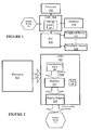
- Figure 1 shows a portion of an exemplary computing system. It comprises a processor 102 (or central processing unit “CPU"), a graphics/memory controller (GMC) 104, an input/output controller (IOC) 106, memory 108, peripheral devices/ports 110, and a display device 112, all coupled together as shown.
- the processor 102 may comprise one or more cores in one or more packages and functions to facilitate central processing tasks including executing one or more applications.
- the GMC 104 controls access to memory 108 from both the processor 102 and IOC 106. It also comprises a graphics processing unit 105 to generate video frames for application(s) running in the processor 102 to be displayed on the display device 112.
- the IOC 106 controls access between the peripheral devices/ports 110 and the other blocks in the system.
- the peripheral devices may include, for example, peripheral chip interconnect (PCI) and/or PCI Express ports, universal serial bus (USB) ports, network (e.g., wireless network) devices, user interface devices such as keypads, mice, and any other devices that may interface with the computing system.
- PCI peripheral chip interconnect
- USB universal serial bus
- network e.g., wireless network
- a performance allocation engine (PAE) 107 is included within the graphics processing unit 105 to allocate performance resources between the graphics processing unit and the processor 102.
- the PAE monitors the rate at which frames are generated by the GPU, as well as a performance utilization metric (e.g., how busy is it?) to control performance resource allocation for the GPU or between the GPU and processor so as to reduce performance resource consumption by the GPU when less performance, e.g., frequency, is needed.
- a performance allocation engine 107 is included in the GPU, it may alternatively be included in any other or combination of GPU and other computing system blocks.
- graphics, memory and I/O controller functionality are implemented in chips separate from the processor chip, but they may also be implemented in a common chip or common integrated circuit (IC) package with different combinations of each other and thus, the invention is not limited to any particular chip or chip combination.
- FIG. 2 shows a portion of a computing system, such as the computing system of Figure 1 , with a portion of a GPU 105 having a performance allocation engine 107.
- the GPU 105 receives frame data, e.g., all or in part generated by an application running in the processor 102.
- the frame rendering engine processes the frame data to generate rendered frames (e.g., files of digital pixel information corresponding to all or part of a video frame) that can be provided to the display device 112.
- the rendered frames are driven into the memory 207, which serves as a buffer, e.g., first-in-first-out frame buffer, to store the frames so that they can be fed into the display device 112 by the display engine 209.
- a buffer e.g., first-in-first-out frame buffer
- frame rendering engine 205 may or may not comprise all or parts of other functional units within or external to the GPU 105.
- the memory 207 may or may not be within the GPU.
- the PAE 107 comprises hardware and or software to allocate performance resources (e.g., frequency) between the GPU 105 and processor 102.
- performance resources e.g., frequency
- it may be implemented as an executable software routine, e.g., in a GPU driver, or it may wholly or partially be implemented with dedicated or shared arithmetic or other logic circuitry.
- it may comprise any suitable combination of hardware and/or software, implemented in and/or external to a GPU to monitor a rendered frame rate, e.g., instantaneous and/or a moving average frame rate, along with GPU processor utilization (e.g., a measure or indication of how hard the frame rendering engine 205 is working) to control, or otherwise indicate, performance resource allocation for the GPU and/or the processor.
- FIG. 3 shows an exemplary flow diagram for implementing a performance allocation engine routine 107.
- the graphs of Figures 4A to 4D will be described to provide an overview for an understanding of the purposes of the routine of Figure 3 .
- These graphs show frame rendering performance as a function of CPU and GPU performance, progressively, as relatively increased performance resources are provided to the processor.
- Each graph includes exemplary average distributions of frame duration for the GPU and processor, i.e., the relative times taken by the processor and GPU to generate frame data and rendered frames, respectively.
- the average rendered frame rate increases.
- Figure 4A represents a situation when the frame rate is completely limited by the processor. Moving from graph 4A to 4D, relatively higher performance resources (frequency in this example) are provided to the processor, thereby shifting the processor distribution curve to the left and thus making the overall frame generation rate less limited by the processor. So, it can be seen that if the overall rendered frame rate is processor limited, then it doesn't materially help to increase GPU performance and conversely, when the rendered frame rate is GPU limited, the frame rate is not materially improved by increasing processor performance.
- GPU performance (and not necessarily processor performance) should be increased. If, however, the frame rate is sufficient, then performance resources can be reduced for the processor and thus, power consumption, for example, may be reduced. Likewise, if it is determined that the frame rate may be processor limited, then if the frame rate is not sufficient, it may be inferred that additional performance resources should be provided to the processor. If, however, the frame rate is deemed to be sufficient, then performance resources may be reduced from the GPU. With this in mind, the flow diagram of Figure 3 will be discussed.
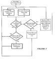
- Figure 3 shows a performance allocation engine routine 302 in accordance with some embodiments.
- the graphics render utilization is evaluated. This, for example, could be done by evaluating utilization in a frame rendering engine such as frame rendering utilization 205 in the GPU 105. Utilization is a measure of how hard the rendering engine is working. It may be as simple as whether or not relevant processing units are active or idle, or it could be a more quantitative measure of the extent to which relevant GPU units are performing.
- the rendered frame rate is evaluated (or monitored). This involves determining the rate at which rendered frames are being generated, e.g., by a frame rendering engine. For example, within the GPU (or even external to it), one or more signals indicative of whether a new frame is being provided to memory (e.g., memory 207) could be monitored to measure or estimate the times between generated frames.
- a frame rendering engine For example, within the GPU (or even external to it), one or more signals indicative of whether a new frame is being provided to memory (e.g., memory 207) could be monitored to measure or estimate the times between generated frames.
- the frame rate used in the routine may be an instantaneous estimate, an average, a moving average with a desired window size (number of frames), or a combination of such rates.
- a weighted average may be used to filter out anomalies. For example, weight values adding up to one could be employed for different adjacent frame durations to calculate a running average. The number of weight values adding up to one would correspond to the number of frames in the moving window. Depending on the sampling rate used to measure frame durations, the values could be adjusted to achieve acceptable results.
- a first weighting constant, a 1 , of 1/30000 and a second weighting constant, a 2 , of 2999/30000 could be used.
- any suitable or otherwise desired weighting scheme or numbers of frames per window could be utilized.
- the routine determines if GPU utilization is high. If it is not high (e.g., normal or low), then at 310, the routine determines if the rendered frame rate is sufficient. If the frame rate is not sufficient (implying that GPU performance is sufficient but processor performance is insufficient), then at 314, the processor performance may be increased. (Note that a dashed box is used here, and elsewhere in this figure, to indicate that control of the processor performance may not be available to the PAE, so it may either control or otherwise indicate that the processor performance should be increased.) On the other hand, if the frame rate at 310 is sufficient, then at 312, the GPU performance is decreased and additional performance is allocated to the processor. From either 312 or 314, the routine loops back to 304 and 306 as shown.
- the routine proceeds to 316 and determines if the rendered frame rate is sufficient (e.g., in the same way as at 310). If the frame rate is sufficient, then the routine loops back to 304 and 306 and proceeds as discussed. On the other hand, if the frame rate is not sufficient (implying that the frame rate is GPU limited), then at 318, the GPU performance is increased (e.g., frequency is increased), and the routine loops back to 304 and 306 and proceeds as discussed.
- Coupled is used to indicate that two or more elements are in direct physical or electrical contact with each other.
- Connected is used to indicate that two or more elements are in direct physical or electrical contact with each other.
- Connected is used to indicate that two or more elements are in direct physical or electrical contact with each other.
- Connected is used to indicate that two or more elements are in direct physical or electrical contact with each other.
- Connected is used to indicate that two or more elements are in direct physical or electrical contact with each other.
- Coupled is used to indicate that two or more elements co-operate or interact with each other, but they may or may not be in direct physical or electrical contact.
- IC semiconductor integrated circuit
- PDA programmable logic arrays
- signal conductor lines are represented with lines. Some may be thicker, to indicate more constituent signal paths, have a number label, to indicate a number of constituent signal paths, and/or have arrows at one or more ends, to indicate primary information flow direction. This, however, should not be construed in a limiting manner. Rather, such added detail may be used in connection with one or more exemplary embodiments to facilitate easier understanding of a circuit. Any represented signal lines, whether or not having additional information, may actually comprise one or more signals that may travel in multiple directions and may be implemented with any suitable type of signal scheme, e.g., digital or analog lines implemented with differential pairs, optical fiber lines, and/or single-ended lines.
Landscapes
- Engineering & Computer Science (AREA)
- Theoretical Computer Science (AREA)
- General Physics & Mathematics (AREA)
- Physics & Mathematics (AREA)
- General Engineering & Computer Science (AREA)
- Software Systems (AREA)
- Computer Hardware Design (AREA)
- Computer Graphics (AREA)
- Multimedia (AREA)
- Controls And Circuits For Display Device (AREA)
- Power Sources (AREA)
- Image Processing (AREA)
- Testing And Monitoring For Control Systems (AREA)
- Debugging And Monitoring (AREA)
- Image Generation (AREA)
Abstract
Description
- The present invention relates generally to computing and in particular to allocating processing resources between core and graphics processing.
- With today's and future computing systems such as desktop computers, mobile computers, portable devices such as phones and audio/video players, and the like, it is desirable to consume less power, regardless of whether or not the device is mobile or otherwise. Accordingly, with many devices that include more than one processing unit such as with a core processing unit (e.g., a core within a processor having one or more processing cores) and a graphics processor, performance budgets may be imposed on the processors (or processing units) to reduce overall power consumption. Unfortunately, such approaches can be inefficient and thus, improved solutions may be desired.
- Embodiments of the invention are illustrated by way of example, and not by way of limitation, in the figures of the accompanying drawings in which like reference numerals refer to similar elements.
-
Figure 1 is a system diagram of a computing system in accordance with some embodiments. -
Figure 2 is a diagram of a portion of a computing system with a performance allocation engine in accordance with some embodiments. -
Figure 3 is a flow diagram of a routine to implement a performance allocation engine in accordance with some embodiments. -
Figures 4A-4D graphically show frame rendering performance as a function of CPU and GPU performance, progressively, as relatively increased performance resources are provided to the CPU. - In accordance with some embodiments, a graphics process frame generation frame rate may be monitored in combination with a utilization or work load metric for the graphics process in order to allocate performance resources to the graphics process and in some cases, between the graphics process and a central processing unit.
-
Figure 1 shows a portion of an exemplary computing system. It comprises a processor 102 (or central processing unit "CPU"), a graphics/memory controller (GMC) 104, an input/output controller (IOC) 106,memory 108, peripheral devices/ports 110, and adisplay device 112, all coupled together as shown. Theprocessor 102 may comprise one or more cores in one or more packages and functions to facilitate central processing tasks including executing one or more applications. - The GMC 104 controls access to
memory 108 from both theprocessor 102 and IOC 106. It also comprises agraphics processing unit 105 to generate video frames for application(s) running in theprocessor 102 to be displayed on thedisplay device 112. - The IOC 106 controls access between the peripheral devices/
ports 110 and the other blocks in the system. The peripheral devices may include, for example, peripheral chip interconnect (PCI) and/or PCI Express ports, universal serial bus (USB) ports, network (e.g., wireless network) devices, user interface devices such as keypads, mice, and any other devices that may interface with the computing system. - In some embodiments, a performance allocation engine (PAE) 107 is included within the
graphics processing unit 105 to allocate performance resources between the graphics processing unit and theprocessor 102. As will be discussed more below, the PAE monitors the rate at which frames are generated by the GPU, as well as a performance utilization metric (e.g., how busy is it?) to control performance resource allocation for the GPU or between the GPU and processor so as to reduce performance resource consumption by the GPU when less performance, e.g., frequency, is needed. (It should be appreciated that while in the depicted embodiment, aperformance allocation engine 107 is included in the GPU, it may alternatively be included in any other or combination of GPU and other computing system blocks. Similarly, it should be appreciated that in the depicted embodiment, graphics, memory and I/O controller functionality are implemented in chips separate from the processor chip, but they may also be implemented in a common chip or common integrated circuit (IC) package with different combinations of each other and thus, the invention is not limited to any particular chip or chip combination.) -
Figure 2 shows a portion of a computing system, such as the computing system ofFigure 1 , with a portion of aGPU 105 having aperformance allocation engine 107. Shown in the GPU, apart from the PAE 107, is aframe rendering engine 205,memory 207, and adisplay engine 209. TheGPU 105 receives frame data, e.g., all or in part generated by an application running in theprocessor 102. The frame rendering engine processes the frame data to generate rendered frames (e.g., files of digital pixel information corresponding to all or part of a video frame) that can be provided to thedisplay device 112. The rendered frames are driven into thememory 207, which serves as a buffer, e.g., first-in-first-out frame buffer, to store the frames so that they can be fed into thedisplay device 112 by thedisplay engine 209. - (It should be appreciated that the frame rendering
engine 205,memory 207, anddisplay engine 209 represent functional blocks that may or may not comprise all or parts of other functional units within or external to theGPU 105. For example, thememory 207 may or may not be within the GPU.) - The PAE 107 comprises hardware and or software to allocate performance resources (e.g., frequency) between the
GPU 105 andprocessor 102. For example, it may be implemented as an executable software routine, e.g., in a GPU driver, or it may wholly or partially be implemented with dedicated or shared arithmetic or other logic circuitry. it may comprise any suitable combination of hardware and/or software, implemented in and/or external to a GPU to monitor a rendered frame rate, e.g., instantaneous and/or a moving average frame rate, along with GPU processor utilization (e.g., a measure or indication of how hard theframe rendering engine 205 is working) to control, or otherwise indicate, performance resource allocation for the GPU and/or the processor. -
Figure 3 shows an exemplary flow diagram for implementing a performanceallocation engine routine 107. However, before discussing it, the graphs ofFigures 4A to 4D will be described to provide an overview for an understanding of the purposes of the routine ofFigure 3 . These graphs show frame rendering performance as a function of CPU and GPU performance, progressively, as relatively increased performance resources are provided to the processor. Each graph includes exemplary average distributions of frame duration for the GPU and processor, i.e., the relative times taken by the processor and GPU to generate frame data and rendered frames, respectively. Thus, as the curves move to the left, and thus frame duration attributable to the GPU and/or processor decrease, the average rendered frame rate increases. -
Figure 4A represents a situation when the frame rate is completely limited by the processor. Moving from graph 4A to 4D, relatively higher performance resources (frequency in this example) are provided to the processor, thereby shifting the processor distribution curve to the left and thus making the overall frame generation rate less limited by the processor. So, it can be seen that if the overall rendered frame rate is processor limited, then it doesn't materially help to increase GPU performance and conversely, when the rendered frame rate is GPU limited, the frame rate is not materially improved by increasing processor performance. - Thus, when rendered frame generation is GPU limited, if the frame rate is not sufficient, GPU performance (and not necessarily processor performance) should be increased. If, however, the frame rate is sufficient, then performance resources can be reduced for the processor and thus, power consumption, for example, may be reduced. Likewise, if it is determined that the frame rate may be processor limited, then if the frame rate is not sufficient, it may be inferred that additional performance resources should be provided to the processor. If, however, the frame rate is deemed to be sufficient, then performance resources may be reduced from the GPU. With this in mind, the flow diagram of
Figure 3 will be discussed. -
Figure 3 shows a performanceallocation engine routine 302 in accordance with some embodiments. At 304, the graphics render utilization is evaluated. This, for example, could be done by evaluating utilization in a frame rendering engine such asframe rendering utilization 205 in the GPU 105. Utilization is a measure of how hard the rendering engine is working. It may be as simple as whether or not relevant processing units are active or idle, or it could be a more quantitative measure of the extent to which relevant GPU units are performing. - At 306, the rendered frame rate is evaluated (or monitored). This involves determining the rate at which rendered frames are being generated, e.g., by a frame rendering engine. For example, within the GPU (or even external to it), one or more signals indicative of whether a new frame is being provided to memory (e.g., memory 207) could be monitored to measure or estimate the times between generated frames.
- The frame rate used in the routine may be an instantaneous estimate, an average, a moving average with a desired window size (number of frames), or a combination of such rates. In some embodiments, a weighted average may be used to filter out anomalies. For example, weight values adding up to one could be employed for different adjacent frame durations to calculate a running average. The number of weight values adding up to one would correspond to the number of frames in the moving window. Depending on the sampling rate used to measure frame durations, the values could be adjusted to achieve acceptable results.
- As an example, with an assumed sampling rate of 200 samples-per-second and a desired moving average window width of 5 seconds with two frames in the window, a first weighting constant, a1, of 1/30000 and a second weighting constant, a2, of 2999/30000 could be used. The MOVING AVERAGE frame rate would then be calculated as:

where Fd[n-1] is the duration of the first frame in a window and Fd is the duration of the next frame in the window. Of course, any suitable or otherwise desired weighting scheme or numbers of frames per window could be utilized. - At 308, it is determined if GPU utilization is high. If it is not high (e.g., normal or low), then at 310, the routine determines if the rendered frame rate is sufficient. If the frame rate is not sufficient (implying that GPU performance is sufficient but processor performance is insufficient), then at 314, the processor performance may be increased. (Note that a dashed box is used here, and elsewhere in this figure, to indicate that control of the processor performance may not be available to the PAE, so it may either control or otherwise indicate that the processor performance should be increased.) On the other hand, if the frame rate at 310 is sufficient, then at 312, the GPU performance is decreased and additional performance is allocated to the processor. From either 312 or 314, the routine loops back to 304 and 306 as shown.
- Returning to 308, if the GPU utilization is high, then the routine proceeds to 316 and determines if the rendered frame rate is sufficient (e.g., in the same way as at 310). If the frame rate is sufficient, then the routine loops back to 304 and 306 and proceeds as discussed. On the other hand, if the frame rate is not sufficient (implying that the frame rate is GPU limited), then at 318, the GPU performance is increased (e.g., frequency is increased), and the routine loops back to 304 and 306 and proceeds as discussed.
- In the preceding description, numerous specific details have been set forth. However, it is understood that embodiments of the invention may be practiced without these specific details. In other instances, well-known circuits, structures and techniques may have not been shown in detail in order not to obscure an understanding of the description. With this in mind, references to "one embodiment", "an embodiment", "example embodiment", "various embodiments", etc., indicate that the embodiment(s) of the invention so described may include particular features, structures, or characteristics, but not every embodiment necessarily includes the particular features, structures, or characteristics. Further, some embodiments may have some, all, or none of the features described for other embodiments.
- In the preceding description and following claims, the following terms should be construed as follows: The terms "coupled" and "connected," along with their derivatives, may be used. It should be understood that these terms are not intended as synonyms for each other. Rather, in particular embodiments, "connected" is used to indicate that two or more elements are in direct physical or electrical contact with each other. "Coupled" is used to indicate that two or more elements co-operate or interact with each other, but they may or may not be in direct physical or electrical contact.
- The invention is not limited to the embodiments described, but can be practiced with modification and alteration within the spirit and scope of the appended claims. For example, it should be appreciated that the present invention is applicable for use with all types of semiconductor integrated circuit ("IC") chips. Examples of these IC chips include but are not limited to processors, controllers, chip set components, programmable logic arrays (PLA), memory chips, network chips, and the like.
- It should also be appreciated that in some of the drawings, signal conductor lines are represented with lines. Some may be thicker, to indicate more constituent signal paths, have a number label, to indicate a number of constituent signal paths, and/or have arrows at one or more ends, to indicate primary information flow direction. This, however, should not be construed in a limiting manner. Rather, such added detail may be used in connection with one or more exemplary embodiments to facilitate easier understanding of a circuit. Any represented signal lines, whether or not having additional information, may actually comprise one or more signals that may travel in multiple directions and may be implemented with any suitable type of signal scheme, e.g., digital or analog lines implemented with differential pairs, optical fiber lines, and/or single-ended lines.
- It should be appreciated that example sizes/models/values/ranges may have been given, although the present invention is not limited to the same. As manufacturing techniques (e.g., photolithography) mature over time, it is expected that devices of smaller size could be manufactured. In addition, well known power/ground connections to IC chips and other components may or may not be shown within the FIGS, for simplicity of illustration and discussion, and so as not to obscure the invention. Further, arrangements may be shown in block diagram form in order to avoid obscuring the invention, and also in view of the fact that specifics with respect to implementation of such block diagram arrangements are highly dependent upon the platform within which the present invention is to be implemented, i.e., such specifics should be well within purview of one skilled in the art. Where specific details (e.g., circuits) are set forth in order to describe example embodiments of the invention, it should be apparent to one skilled in the art that the invention can be practiced without, or with variation of, these specific details. The description is thus to be regarded as illustrative instead of limiting.
Claims (20)
- A chip, comprising:a performance allocation engine (PAE) to monitor a utilization for a graphics process that is rendering frames and to monitor a frame rate for the rendered frames in order to allocate performance resources for the graphics process.
- The chip of claim 1, in which the performance allocation engine allocates performance resources to a central processor, as well as to the graphics process.
- The chip of claim 2, in which the performance allocation engine is implemented as executable instructions in a graphics processor driver, the graphics process being performed in the graphics processor.
- The chip of claim 3, in which the graphics processor receives frame data from the central processor.
- The chip of claim 4, in which the central processor comprises multiple cores, one or more of which is to generate the frame data.
- The chip of claim 4, in which the PAE is to reduce performance resources from the graphics process in response to determining that the frame rate is insufficient and the graphics process utilization is not high.
- The chip of claim 6, in which the PAE is to provide the performance resources reduced from the graphics process to the central processor.
- The chip of claim 1, in which the performance resources include operating frequency.
- A method, comprising:monitoring a graphics processor work load;monitoring the rate at which the graphics processor generates frames; andallocating performance resources to the graphics processor based on the monitored work load and monitored frame rate.
- The method of claim 9, in which monitoring work load comprises determining if frame rendering units in the graphics processor are active for a substantial amount of time.
- The method of claim 10, further comprising determining if a sufficient number of frame rendering units are substantially active.
- The method of claim 9, in which monitoring work load comprises monitoring whether or not the graphics processor is idle.
- The method of claim 12, further comprising determining an idle duty cycle for the graphics processor.
- The method of claim 9, comprising less performance resources to the graphics processor if the frame rate is sufficient and the work load is sufficiently low.
- The method of claim 14, in which additional performance resources are provided to a central processor if the frame rate is sufficient and the work load is sufficiently low.
- A system, comprising:a first processor to execute an application and generate frame data from the executed application;a graphics processor to receive the frame data and to generate rendered frames therefrom; anda performance allocation engine to monitor a utilization metric for the graphics processor, to monitor a rate at which the rendered frames are being generated, and to allocate performance resources to the graphics processor based on the monitored utilization metric and frame rate.
- The system of claim 16, in which the first processor is a central processor.
- The system of claim 116, in which the first processor and graphics processor are part of a common package.
- The system of claim 18, in which the first and graphics processor are on a common die.
- The system of claim 16, comprising a display device to receive the rendered frames in a suitable form.
Applications Claiming Priority (1)
| Application Number | Priority Date | Filing Date | Title |
|---|---|---|---|
| US12/157,479 US8199158B2 (en) | 2008-06-11 | 2008-06-11 | Performance allocation method and apparatus |
Publications (3)
| Publication Number | Publication Date |
|---|---|
| EP2178080A2 true EP2178080A2 (en) | 2010-04-21 |
| EP2178080A3 EP2178080A3 (en) | 2010-11-17 |
| EP2178080B1 EP2178080B1 (en) | 2014-12-17 |
Family
ID=41414320
Family Applications (1)
| Application Number | Title | Priority Date | Filing Date |
|---|---|---|---|
| EP09251531.1A Active EP2178080B1 (en) | 2008-06-11 | 2009-06-11 | Performance allocation method and apparatus |
Country Status (4)
| Country | Link |
|---|---|
| US (3) | US8199158B2 (en) |
| EP (1) | EP2178080B1 (en) |
| KR (1) | KR101129820B1 (en) |
| CN (2) | CN101609545B (en) |
Cited By (1)
| Publication number | Priority date | Publication date | Assignee | Title |
|---|---|---|---|---|
| CN108874544A (en) * | 2018-06-11 | 2018-11-23 | 郑州云海信息技术有限公司 | A kind of method and system of GPU server I/O resource allocation |
Families Citing this family (67)
| Publication number | Priority date | Publication date | Assignee | Title |
|---|---|---|---|---|
| US8199158B2 (en) | 2008-06-11 | 2012-06-12 | Intel Corporation | Performance allocation method and apparatus |
| GB0921831D0 (en) | 2009-12-14 | 2010-01-27 | British Telecomm | Graphical data delivery |
| GB201000738D0 (en) | 2010-01-18 | 2010-03-03 | British Telecomm | Graphical data processing |
| US8730251B2 (en) * | 2010-06-07 | 2014-05-20 | Apple Inc. | Switching video streams for a display without a visible interruption |
| US8933948B2 (en) | 2010-10-01 | 2015-01-13 | Apple Inc. | Graphics system which utilizes fine grained analysis to determine performance issues |
| US8462166B2 (en) | 2010-10-01 | 2013-06-11 | Apple Inc. | Graphics system which measures CPU and GPU performance |
| US8527239B2 (en) | 2010-10-01 | 2013-09-03 | Apple Inc. | Automatic detection of performance bottlenecks in a graphics system |
| US8614716B2 (en) | 2010-10-01 | 2013-12-24 | Apple Inc. | Recording a command stream with a rich encoding format for capture and playback of graphics content |
| US8830245B2 (en) * | 2010-12-14 | 2014-09-09 | Amazon Technologies, Inc. | Load balancing between general purpose processors and graphics processors |
| US8922567B2 (en) * | 2011-03-11 | 2014-12-30 | Broadcom Corporation | Regulation of screen composing in a device |
| US8924752B1 (en) | 2011-04-20 | 2014-12-30 | Apple Inc. | Power management for a graphics processing unit or other circuit |
| US9086883B2 (en) * | 2011-06-10 | 2015-07-21 | Qualcomm Incorporated | System and apparatus for consolidated dynamic frequency/voltage control |
| KR20130019674A (en) * | 2011-08-17 | 2013-02-27 | 삼성전자주식회사 | Terminal and method for performing application thereof |
| KR101845328B1 (en) * | 2011-08-22 | 2018-04-04 | 삼성전자 주식회사 | Terminal and method for performing application thereof |
| US8780120B2 (en) * | 2011-10-02 | 2014-07-15 | Microsoft Corporation | GPU self throttling |
| US9298586B2 (en) | 2011-10-11 | 2016-03-29 | Apple Inc. | Suspending and resuming a graphics application executing on a target device for debugging |
| US8856566B1 (en) | 2011-12-15 | 2014-10-07 | Apple Inc. | Power management scheme that accumulates additional off time for device when no work is available and permits additional power consumption by device when awakened |
| US9304570B2 (en) * | 2011-12-15 | 2016-04-05 | Intel Corporation | Method, apparatus, and system for energy efficiency and energy conservation including power and performance workload-based balancing between multiple processing elements |
| JP5842601B2 (en) * | 2011-12-26 | 2016-01-13 | 富士通株式会社 | Program, information processing method and information processing apparatus |
| KR101229851B1 (en) * | 2011-12-27 | 2013-02-05 | 한국과학기술원 | Data parallel deduplication system |
| US9390461B1 (en) | 2012-05-08 | 2016-07-12 | Apple Inc. | Graphics hardware mode controls |
| TW201349167A (en) * | 2012-05-22 | 2013-12-01 | Hon Hai Prec Ind Co Ltd | Display card device |
| US9250665B2 (en) | 2012-06-07 | 2016-02-02 | Apple Inc. | GPU with dynamic performance adjustment |
| KR101472493B1 (en) * | 2012-06-15 | 2014-12-12 | 건국대학교 산학협력단 | High-Speed Implementations system of Rainbow Method on GPU and the method thereof |
| EP2880622B1 (en) | 2012-07-31 | 2020-11-04 | Intel Corporation | Hybrid rendering systems and methods |
| KR20140030823A (en) * | 2012-09-04 | 2014-03-12 | 삼성전자주식회사 | Soc performing dynamic voltage and frequency scaling policies using 3d workload and method using the same |
| US9342122B2 (en) | 2012-09-17 | 2016-05-17 | Intel Corporation | Distributing power to heterogeneous compute elements of a processor |
| EP2909696A4 (en) * | 2012-10-16 | 2017-02-22 | Razer (Asia-Pacific) Pte. Ltd. | Computing systems and methods for controlling a computing system |
| US9269120B2 (en) * | 2012-11-06 | 2016-02-23 | Intel Corporation | Dynamically rebalancing graphics processor resources |
| US9128721B2 (en) * | 2012-12-11 | 2015-09-08 | Apple Inc. | Closed loop CPU performance control |
| US9275601B2 (en) * | 2012-12-12 | 2016-03-01 | Intel Corporation | Techniques to control frame display rate |
| US9195285B2 (en) * | 2012-12-27 | 2015-11-24 | Intel Corporation | Techniques for platform duty cycling |
| US9424620B2 (en) * | 2012-12-29 | 2016-08-23 | Intel Corporation | Identification of GPU phase to determine GPU scalability during runtime |
| KR20140088691A (en) * | 2013-01-03 | 2014-07-11 | 삼성전자주식회사 | System on chip performing dynamic voltage and frequency scaling policies and method using the same |
| US9201487B2 (en) | 2013-03-05 | 2015-12-01 | Intel Corporation | Reducing power consumption during graphics rendering |
| CA2902292C (en) | 2013-03-15 | 2024-05-21 | Ologn Technologies Ag | Systems, methods and apparatuses for securely storing and providing payment information |
| US9378536B2 (en) * | 2014-04-30 | 2016-06-28 | Qualcomm Incorporated | CPU/GPU DCVS co-optimization for reducing power consumption in graphics frame processing |
| US9645916B2 (en) | 2014-05-30 | 2017-05-09 | Apple Inc. | Performance testing for blocks of code |
| CN104932659B (en) * | 2015-07-15 | 2020-01-07 | 京东方科技集团股份有限公司 | Image display method and display system |
| EP3125072B8 (en) * | 2015-07-29 | 2018-11-14 | Samsung Electronics Co., Ltd. | Method of managing power and electronic device |
| GB2540804B (en) * | 2015-07-29 | 2018-03-07 | Samsung Electronics Co Ltd | Hardware power management apparatus and methods |
| CN106708499B (en) | 2015-11-13 | 2020-10-27 | 财团法人工业技术研究院 | Analysis method and analysis system of drawing processing program |
| US9817431B2 (en) * | 2016-02-03 | 2017-11-14 | Qualcomm Incorporated | Frame based clock rate adjustment for processing unit |
| US20170244894A1 (en) * | 2016-02-22 | 2017-08-24 | Seastar Labs, Inc. | Method and Apparatus for Managing Latency of Remote Video Production |
| CN106095047B (en) * | 2016-05-31 | 2020-07-24 | 联想(北京)有限公司 | Control method and electronic equipment |
| US10331195B2 (en) * | 2016-06-06 | 2019-06-25 | Qualcomm Incorporated | Power and performance aware memory-controller voting mechanism |
| CN106020990B (en) * | 2016-06-30 | 2020-01-10 | 宇龙计算机通信科技(深圳)有限公司 | Control method of central processing unit and terminal equipment |
| CN106454312A (en) * | 2016-09-29 | 2017-02-22 | 乐视控股(北京)有限公司 | Image processing method and device |
| US10845865B2 (en) | 2017-04-21 | 2020-11-24 | Intel Corporation | Reducing power consumption when transferring frames from graphics processors to display panels |
| US10504259B2 (en) | 2017-04-24 | 2019-12-10 | Intel Corporation | Separately processing regions or objects or interest from a render engine to a display engine or a display panel |
| US11404023B2 (en) | 2018-03-26 | 2022-08-02 | Huawei Device Co., Ltd. | Frame rate adjustment method and terminal |
| WO2020062052A1 (en) * | 2018-09-28 | 2020-04-02 | Qualcomm Incorporated | Smart and dynamic janks reduction technology |
| CN109960584A (en) * | 2019-01-30 | 2019-07-02 | 努比亚技术有限公司 | CPU frequency modulation control method, terminal and computer readable storage medium |
| US12131185B2 (en) * | 2019-05-08 | 2024-10-29 | Telefonaktiebolaget Lm Ericsson (Publ) | Sharing and oversubscription of general-purpose graphical processing units in data centers |
| KR20210097938A (en) | 2020-01-31 | 2021-08-10 | 에스케이하이닉스 주식회사 | Apparatus and method for verifying reliability of data read from memory device through clock modulation and memory system including the same |
| KR102713219B1 (en) | 2019-09-02 | 2024-10-07 | 에스케이하이닉스 주식회사 | Memory controller and operating method thereof |
| US12223195B2 (en) | 2019-09-02 | 2025-02-11 | SK Hynix Inc. | Memory controller and operating method thereof |
| CN110532100B (en) * | 2019-09-02 | 2022-04-15 | Oppo广东移动通信有限公司 | Method, device, terminal and storage medium for scheduling resources |
| US12051470B2 (en) | 2019-09-02 | 2024-07-30 | SK Hynix Inc. | Memory controller and operating method thereof |
| US11501808B2 (en) | 2019-09-02 | 2022-11-15 | SK Hynix Inc. | Memory controller and operating method thereof |
| US11507310B2 (en) | 2019-09-02 | 2022-11-22 | SK Hynix Inc. | Memory controller and operating method thereof |
| KR20210061174A (en) | 2019-11-19 | 2021-05-27 | 에스케이하이닉스 주식회사 | Memory controller and operating method thereof |
| KR102862943B1 (en) * | 2020-02-10 | 2025-09-22 | 삼성전자 주식회사 | Electronic device for controlling processing unit based on a time spent in generating a frame and a maximum allowed time and a method for the same |
| US11467621B2 (en) * | 2020-02-28 | 2022-10-11 | Qualcomm Incorporated | Computer processing unit intra-frame clock and voltage scaling based on graphics application awareness |
| US12028548B2 (en) * | 2021-04-19 | 2024-07-02 | Synamedia Limited | Rendering video frames for a user interface operation performed at a client device |
| US12333336B2 (en) | 2021-09-24 | 2025-06-17 | Ati Technologies Ulc | Scheduling and clock management for real-time system quality of service (QoS) |
| CN114510406B (en) * | 2022-02-08 | 2024-07-02 | 北京字节跳动网络技术有限公司 | Method for detecting frame rate and related equipment |
Citations (1)
| Publication number | Priority date | Publication date | Assignee | Title |
|---|---|---|---|---|
| US20040039954A1 (en) | 2002-08-22 | 2004-02-26 | Nvidia, Corp. | Method and apparatus for adaptive power consumption |
Family Cites Families (25)
| Publication number | Priority date | Publication date | Assignee | Title |
|---|---|---|---|---|
| US7149909B2 (en) * | 2002-05-09 | 2006-12-12 | Intel Corporation | Power management for an integrated graphics device |
| US6950105B2 (en) * | 2002-06-03 | 2005-09-27 | Ati Technologies Inc. | Power consumption management in a video graphics accelerator |
| US7268779B2 (en) * | 2002-12-24 | 2007-09-11 | Intel Corporation | Z-buffering techniques for graphics rendering |
| US7119803B2 (en) * | 2002-12-30 | 2006-10-10 | Intel Corporation | Method, apparatus and article for display unit power management |
| US6971034B2 (en) * | 2003-01-09 | 2005-11-29 | Intel Corporation | Power/performance optimized memory controller considering processor power states |
| US7075541B2 (en) | 2003-08-18 | 2006-07-11 | Nvidia Corporation | Adaptive load balancing in a multi-processor graphics processing system |
| US7903116B1 (en) * | 2003-10-27 | 2011-03-08 | Nvidia Corporation | Method, apparatus, and system for adaptive performance level management of a graphics system |
| US7289125B2 (en) * | 2004-02-27 | 2007-10-30 | Nvidia Corporation | Graphics device clustering with PCI-express |
| US7698575B2 (en) * | 2004-03-30 | 2010-04-13 | Intel Corporation | Managing power consumption by requesting an adjustment to an operating point of a processor |
| WO2006034034A2 (en) * | 2004-09-16 | 2006-03-30 | Nvidia Corporation | Load balancing |
| US7898545B1 (en) * | 2004-12-14 | 2011-03-01 | Nvidia Corporation | Apparatus, system, and method for integrated heterogeneous processors |
| US7222253B2 (en) * | 2004-12-28 | 2007-05-22 | Intel Corporation | Dynamic power control for reducing voltage level of graphics controller component of memory controller based on its degree of idleness |
| US7925899B2 (en) * | 2005-12-29 | 2011-04-12 | Intel Corporation | Method, system, and apparatus for runtime power estimation |
| US8102398B2 (en) * | 2006-03-03 | 2012-01-24 | Ati Technologies Ulc | Dynamically controlled power reduction method and circuit for a graphics processor |
| US8314806B2 (en) * | 2006-04-13 | 2012-11-20 | Intel Corporation | Low power display mode |
| US7500041B2 (en) * | 2006-06-15 | 2009-03-03 | Nvidia Corporation | Graphics processing unit for cost effective high performance graphics system with two or more graphics processing units |
| US7412554B2 (en) * | 2006-06-15 | 2008-08-12 | Nvidia Corporation | Bus interface controller for cost-effective high performance graphics system with two or more graphics processing units |
| US8126993B2 (en) * | 2006-07-18 | 2012-02-28 | Nvidia Corporation | System, method, and computer program product for communicating sub-device state information |
| JP2008071261A (en) | 2006-09-15 | 2008-03-27 | Toshiba Corp | Image processing system and image processing method |
| KR101467558B1 (en) * | 2007-07-26 | 2014-12-01 | 엘지전자 주식회사 | A apparatus and a method of graphic data processing |
| US7711864B2 (en) * | 2007-08-31 | 2010-05-04 | Apple Inc. | Methods and systems to dynamically manage performance states in a data processing system |
| US8458497B2 (en) * | 2007-10-11 | 2013-06-04 | Qualcomm Incorporated | Demand based power control in a graphics processing unit |
| US8243085B2 (en) * | 2007-12-30 | 2012-08-14 | Intel Corporation | Boosting graphics performance based on executing workload |
| US8199158B2 (en) | 2008-06-11 | 2012-06-12 | Intel Corporation | Performance allocation method and apparatus |
| US8386808B2 (en) * | 2008-12-22 | 2013-02-26 | Intel Corporation | Adaptive power budget allocation between multiple components in a computing system |
-
2008
- 2008-06-11 US US12/157,479 patent/US8199158B2/en active Active
-
2009
- 2009-06-10 KR KR1020090051431A patent/KR101129820B1/en not_active Expired - Fee Related
- 2009-06-11 EP EP09251531.1A patent/EP2178080B1/en active Active
- 2009-06-11 CN CN200910145948.5A patent/CN101609545B/en active Active
- 2009-06-11 CN CN201310722006.5A patent/CN103927708B/en active Active
-
2012
- 2012-05-11 US US13/469,395 patent/US8411095B2/en not_active Expired - Fee Related
-
2013
- 2013-02-28 US US13/780,523 patent/US9142001B2/en active Active
Patent Citations (1)
| Publication number | Priority date | Publication date | Assignee | Title |
|---|---|---|---|---|
| US20040039954A1 (en) | 2002-08-22 | 2004-02-26 | Nvidia, Corp. | Method and apparatus for adaptive power consumption |
Cited By (1)
| Publication number | Priority date | Publication date | Assignee | Title |
|---|---|---|---|---|
| CN108874544A (en) * | 2018-06-11 | 2018-11-23 | 郑州云海信息技术有限公司 | A kind of method and system of GPU server I/O resource allocation |
Also Published As
| Publication number | Publication date |
|---|---|
| US20090309885A1 (en) | 2009-12-17 |
| CN103927708B (en) | 2017-07-21 |
| EP2178080B1 (en) | 2014-12-17 |
| US9142001B2 (en) | 2015-09-22 |
| US8199158B2 (en) | 2012-06-12 |
| CN101609545A (en) | 2009-12-23 |
| CN103927708A (en) | 2014-07-16 |
| US8411095B2 (en) | 2013-04-02 |
| CN101609545B (en) | 2014-03-05 |
| KR20090129355A (en) | 2009-12-16 |
| US20120223954A1 (en) | 2012-09-06 |
| EP2178080A3 (en) | 2010-11-17 |
| US20130229420A1 (en) | 2013-09-05 |
| KR101129820B1 (en) | 2012-04-13 |
Similar Documents
| Publication | Publication Date | Title |
|---|---|---|
| EP2178080A2 (en) | Performance allocation method and apparatus | |
| JP5923627B2 (en) | Method and apparatus for coordinating I/O channels on a virtual platform - Patents.com | |
| US8527794B2 (en) | Realtime power management of integrated circuits | |
| US10133336B2 (en) | Dynamically entering low power states during active workloads | |
| CN111190739B (en) | Resource allocation method and device, electronic equipment and storage medium | |
| US9389921B2 (en) | System and method for flexible device driver resource allocation | |
| JP2018533112A (en) | GPU workload characterization and power management using command stream hints | |
| CN108415772B (en) | Container-based resource adjustment method, device and medium | |
| CN105677000B (en) | The system and method for dynamic voltage frequency adjustment | |
| CN103763346A (en) | Distributed resource scheduling method and device | |
| CN112463367A (en) | Method and system for optimizing performance of storage system, electronic equipment and storage medium | |
| CN107624181B (en) | Virtual machine management method and apparatus including idling and scheduling of virtual processors | |
| KR101454219B1 (en) | Method of power management for graphic processing unit and system thereof | |
| CN110113269A (en) | A kind of method and relevant apparatus of the flow control based on middleware | |
| CN103870331A (en) | Dynamic processor core distribution method and electronic equipment | |
| CN102982536B (en) | Image processing method and device | |
| CN105094944A (en) | Virtual machine migration method and apparatus | |
| WO2025080331A1 (en) | Processor unit scheduling based on die plan in multi-cluster architectures | |
| CN109871112B (en) | An Openpower system performance-power consumption ratio optimized display system | |
| CN117234744B (en) | Multi-chip system performance optimization method, system, electronic equipment and medium | |
| US10678568B2 (en) | System resource allocation in respect of display interfaces | |
| CN115827541B (en) | Data transmission method, device, SOC chip, electronic component and electronic equipment | |
| CN1540473B (en) | Automatic adjusting device and method for computer system efficiency | |
| CN114579295A (en) | Method for adaptively calling external hardware resource | |
| CN120723576A (en) | Processor optimization method, device, equipment and storage medium |
Legal Events
| Date | Code | Title | Description |
|---|---|---|---|
| PUAI | Public reference made under article 153(3) epc to a published international application that has entered the european phase |
Free format text: ORIGINAL CODE: 0009012 |
|
| 17P | Request for examination filed |
Effective date: 20090701 |
|
| AK | Designated contracting states |
Kind code of ref document: A2 Designated state(s): AT BE BG CH CY CZ DE DK EE ES FI FR GB GR HR HU IE IS IT LI LT LU LV MC MK MT NL NO PL PT RO SE SI SK TR |
|
| AX | Request for extension of the european patent |
Extension state: AL BA RS |
|
| PUAL | Search report despatched |
Free format text: ORIGINAL CODE: 0009013 |
|
| RIC1 | Information provided on ipc code assigned before grant |
Ipc: G09G 5/00 20060101AFI20100317BHEP Ipc: G09G 5/36 20060101ALI20101007BHEP Ipc: G06F 11/34 20060101ALI20101007BHEP |
|
| AK | Designated contracting states |
Kind code of ref document: A3 Designated state(s): AT BE BG CH CY CZ DE DK EE ES FI FR GB GR HR HU IE IS IT LI LT LU LV MC MK MT NL NO PL PT RO SE SI SK TR |
|
| AX | Request for extension of the european patent |
Extension state: AL BA RS |
|
| 17Q | First examination report despatched |
Effective date: 20101102 |
|
| REG | Reference to a national code |
Ref country code: DE Ref legal event code: R079 Ref document number: 602009028353 Country of ref document: DE Free format text: PREVIOUS MAIN CLASS: G09G0005000000 Ipc: G06F0001320000 |
|
| GRAP | Despatch of communication of intention to grant a patent |
Free format text: ORIGINAL CODE: EPIDOSNIGR1 |
|
| RIC1 | Information provided on ipc code assigned before grant |
Ipc: G06F 11/34 20060101ALI20140714BHEP Ipc: G06T 1/00 20060101ALI20140714BHEP Ipc: G09G 5/36 20060101ALI20140714BHEP Ipc: G09G 5/00 20060101ALI20140714BHEP Ipc: G06F 9/50 20060101ALI20140714BHEP Ipc: G06F 1/32 20060101AFI20140714BHEP Ipc: G06T 1/20 20060101ALI20140714BHEP |
|
| INTG | Intention to grant announced |
Effective date: 20140807 |
|
| GRAS | Grant fee paid |
Free format text: ORIGINAL CODE: EPIDOSNIGR3 |
|
| GRAA | (expected) grant |
Free format text: ORIGINAL CODE: 0009210 |
|
| AK | Designated contracting states |
Kind code of ref document: B1 Designated state(s): AT BE BG CH CY CZ DE DK EE ES FI FR GB GR HR HU IE IS IT LI LT LU LV MC MK MT NL NO PL PT RO SE SI SK TR |
|
| REG | Reference to a national code |
Ref country code: GB Ref legal event code: FG4D |
|
| REG | Reference to a national code |
Ref country code: CH Ref legal event code: EP |
|
| REG | Reference to a national code |
Ref country code: IE Ref legal event code: FG4D |
|
| REG | Reference to a national code |
Ref country code: AT Ref legal event code: REF Ref document number: 702334 Country of ref document: AT Kind code of ref document: T Effective date: 20150115 |
|
| REG | Reference to a national code |
Ref country code: DE Ref legal event code: R096 Ref document number: 602009028353 Country of ref document: DE Effective date: 20150129 |
|
| PG25 | Lapsed in a contracting state [announced via postgrant information from national office to epo] |
Ref country code: NO Free format text: LAPSE BECAUSE OF FAILURE TO SUBMIT A TRANSLATION OF THE DESCRIPTION OR TO PAY THE FEE WITHIN THE PRESCRIBED TIME-LIMIT Effective date: 20150317 Ref country code: FI Free format text: LAPSE BECAUSE OF FAILURE TO SUBMIT A TRANSLATION OF THE DESCRIPTION OR TO PAY THE FEE WITHIN THE PRESCRIBED TIME-LIMIT Effective date: 20141217 Ref country code: LT Free format text: LAPSE BECAUSE OF FAILURE TO SUBMIT A TRANSLATION OF THE DESCRIPTION OR TO PAY THE FEE WITHIN THE PRESCRIBED TIME-LIMIT Effective date: 20141217 |
|
| REG | Reference to a national code |
Ref country code: LT Ref legal event code: MG4D |
|
| PG25 | Lapsed in a contracting state [announced via postgrant information from national office to epo] |
Ref country code: SE Free format text: LAPSE BECAUSE OF FAILURE TO SUBMIT A TRANSLATION OF THE DESCRIPTION OR TO PAY THE FEE WITHIN THE PRESCRIBED TIME-LIMIT Effective date: 20141217 Ref country code: GR Free format text: LAPSE BECAUSE OF FAILURE TO SUBMIT A TRANSLATION OF THE DESCRIPTION OR TO PAY THE FEE WITHIN THE PRESCRIBED TIME-LIMIT Effective date: 20150318 Ref country code: LV Free format text: LAPSE BECAUSE OF FAILURE TO SUBMIT A TRANSLATION OF THE DESCRIPTION OR TO PAY THE FEE WITHIN THE PRESCRIBED TIME-LIMIT Effective date: 20141217 Ref country code: HR Free format text: LAPSE BECAUSE OF FAILURE TO SUBMIT A TRANSLATION OF THE DESCRIPTION OR TO PAY THE FEE WITHIN THE PRESCRIBED TIME-LIMIT Effective date: 20141217 |
|
| REG | Reference to a national code |
Ref country code: AT Ref legal event code: MK05 Ref document number: 702334 Country of ref document: AT Kind code of ref document: T Effective date: 20141217 |
|
| PG25 | Lapsed in a contracting state [announced via postgrant information from national office to epo] |
Ref country code: NL Free format text: LAPSE BECAUSE OF FAILURE TO SUBMIT A TRANSLATION OF THE DESCRIPTION OR TO PAY THE FEE WITHIN THE PRESCRIBED TIME-LIMIT Effective date: 20141217 |
|
| PG25 | Lapsed in a contracting state [announced via postgrant information from national office to epo] |
Ref country code: ES Free format text: LAPSE BECAUSE OF FAILURE TO SUBMIT A TRANSLATION OF THE DESCRIPTION OR TO PAY THE FEE WITHIN THE PRESCRIBED TIME-LIMIT Effective date: 20141217 Ref country code: EE Free format text: LAPSE BECAUSE OF FAILURE TO SUBMIT A TRANSLATION OF THE DESCRIPTION OR TO PAY THE FEE WITHIN THE PRESCRIBED TIME-LIMIT Effective date: 20141217 Ref country code: SK Free format text: LAPSE BECAUSE OF FAILURE TO SUBMIT A TRANSLATION OF THE DESCRIPTION OR TO PAY THE FEE WITHIN THE PRESCRIBED TIME-LIMIT Effective date: 20141217 Ref country code: CZ Free format text: LAPSE BECAUSE OF FAILURE TO SUBMIT A TRANSLATION OF THE DESCRIPTION OR TO PAY THE FEE WITHIN THE PRESCRIBED TIME-LIMIT Effective date: 20141217 Ref country code: RO Free format text: LAPSE BECAUSE OF FAILURE TO SUBMIT A TRANSLATION OF THE DESCRIPTION OR TO PAY THE FEE WITHIN THE PRESCRIBED TIME-LIMIT Effective date: 20141217 |
|
| PG25 | Lapsed in a contracting state [announced via postgrant information from national office to epo] |
Ref country code: AT Free format text: LAPSE BECAUSE OF FAILURE TO SUBMIT A TRANSLATION OF THE DESCRIPTION OR TO PAY THE FEE WITHIN THE PRESCRIBED TIME-LIMIT Effective date: 20141217 Ref country code: IS Free format text: LAPSE BECAUSE OF FAILURE TO SUBMIT A TRANSLATION OF THE DESCRIPTION OR TO PAY THE FEE WITHIN THE PRESCRIBED TIME-LIMIT Effective date: 20150417 Ref country code: PL Free format text: LAPSE BECAUSE OF FAILURE TO SUBMIT A TRANSLATION OF THE DESCRIPTION OR TO PAY THE FEE WITHIN THE PRESCRIBED TIME-LIMIT Effective date: 20141217 |
|
| REG | Reference to a national code |
Ref country code: DE Ref legal event code: R097 Ref document number: 602009028353 Country of ref document: DE |
|
| PLBE | No opposition filed within time limit |
Free format text: ORIGINAL CODE: 0009261 |
|
| STAA | Information on the status of an ep patent application or granted ep patent |
Free format text: STATUS: NO OPPOSITION FILED WITHIN TIME LIMIT |
|
| PG25 | Lapsed in a contracting state [announced via postgrant information from national office to epo] |
Ref country code: DK Free format text: LAPSE BECAUSE OF FAILURE TO SUBMIT A TRANSLATION OF THE DESCRIPTION OR TO PAY THE FEE WITHIN THE PRESCRIBED TIME-LIMIT Effective date: 20141217 |
|
| 26N | No opposition filed |
Effective date: 20150918 |
|
| PG25 | Lapsed in a contracting state [announced via postgrant information from national office to epo] |
Ref country code: IT Free format text: LAPSE BECAUSE OF FAILURE TO SUBMIT A TRANSLATION OF THE DESCRIPTION OR TO PAY THE FEE WITHIN THE PRESCRIBED TIME-LIMIT Effective date: 20141217 |
|
| PG25 | Lapsed in a contracting state [announced via postgrant information from national office to epo] |
Ref country code: MC Free format text: LAPSE BECAUSE OF FAILURE TO SUBMIT A TRANSLATION OF THE DESCRIPTION OR TO PAY THE FEE WITHIN THE PRESCRIBED TIME-LIMIT Effective date: 20141217 |
|
| REG | Reference to a national code |
Ref country code: CH Ref legal event code: PL |
|
| PG25 | Lapsed in a contracting state [announced via postgrant information from national office to epo] |
Ref country code: SI Free format text: LAPSE BECAUSE OF FAILURE TO SUBMIT A TRANSLATION OF THE DESCRIPTION OR TO PAY THE FEE WITHIN THE PRESCRIBED TIME-LIMIT Effective date: 20141217 Ref country code: LU Free format text: LAPSE BECAUSE OF FAILURE TO SUBMIT A TRANSLATION OF THE DESCRIPTION OR TO PAY THE FEE WITHIN THE PRESCRIBED TIME-LIMIT Effective date: 20150611 |
|
| REG | Reference to a national code |
Ref country code: IE Ref legal event code: MM4A |
|
| PG25 | Lapsed in a contracting state [announced via postgrant information from national office to epo] |
Ref country code: CH Free format text: LAPSE BECAUSE OF NON-PAYMENT OF DUE FEES Effective date: 20150630 Ref country code: LI Free format text: LAPSE BECAUSE OF NON-PAYMENT OF DUE FEES Effective date: 20150630 Ref country code: IE Free format text: LAPSE BECAUSE OF NON-PAYMENT OF DUE FEES Effective date: 20150611 |
|
| REG | Reference to a national code |
Ref country code: FR Ref legal event code: PLFP Year of fee payment: 8 |
|
| PG25 | Lapsed in a contracting state [announced via postgrant information from national office to epo] |
Ref country code: BE Free format text: LAPSE BECAUSE OF FAILURE TO SUBMIT A TRANSLATION OF THE DESCRIPTION OR TO PAY THE FEE WITHIN THE PRESCRIBED TIME-LIMIT Effective date: 20141217 |
|
| PG25 | Lapsed in a contracting state [announced via postgrant information from national office to epo] |
Ref country code: MT Free format text: LAPSE BECAUSE OF FAILURE TO SUBMIT A TRANSLATION OF THE DESCRIPTION OR TO PAY THE FEE WITHIN THE PRESCRIBED TIME-LIMIT Effective date: 20141217 |
|
| REG | Reference to a national code |
Ref country code: FR Ref legal event code: PLFP Year of fee payment: 9 |
|
| PG25 | Lapsed in a contracting state [announced via postgrant information from national office to epo] |
Ref country code: BG Free format text: LAPSE BECAUSE OF FAILURE TO SUBMIT A TRANSLATION OF THE DESCRIPTION OR TO PAY THE FEE WITHIN THE PRESCRIBED TIME-LIMIT Effective date: 20141217 Ref country code: HU Free format text: LAPSE BECAUSE OF FAILURE TO SUBMIT A TRANSLATION OF THE DESCRIPTION OR TO PAY THE FEE WITHIN THE PRESCRIBED TIME-LIMIT; INVALID AB INITIO Effective date: 20090611 |
|
| PG25 | Lapsed in a contracting state [announced via postgrant information from national office to epo] |
Ref country code: CY Free format text: LAPSE BECAUSE OF FAILURE TO SUBMIT A TRANSLATION OF THE DESCRIPTION OR TO PAY THE FEE WITHIN THE PRESCRIBED TIME-LIMIT Effective date: 20141217 |
|
| PG25 | Lapsed in a contracting state [announced via postgrant information from national office to epo] |
Ref country code: TR Free format text: LAPSE BECAUSE OF FAILURE TO SUBMIT A TRANSLATION OF THE DESCRIPTION OR TO PAY THE FEE WITHIN THE PRESCRIBED TIME-LIMIT Effective date: 20141217 |
|
| REG | Reference to a national code |
Ref country code: FR Ref legal event code: PLFP Year of fee payment: 10 |
|
| PG25 | Lapsed in a contracting state [announced via postgrant information from national office to epo] |
Ref country code: MK Free format text: LAPSE BECAUSE OF FAILURE TO SUBMIT A TRANSLATION OF THE DESCRIPTION OR TO PAY THE FEE WITHIN THE PRESCRIBED TIME-LIMIT Effective date: 20141217 |
|
| PG25 | Lapsed in a contracting state [announced via postgrant information from national office to epo] |
Ref country code: PT Free format text: LAPSE BECAUSE OF FAILURE TO SUBMIT A TRANSLATION OF THE DESCRIPTION OR TO PAY THE FEE WITHIN THE PRESCRIBED TIME-LIMIT Effective date: 20141217 |
|
| P01 | Opt-out of the competence of the unified patent court (upc) registered |
Effective date: 20230518 |
|
| PGFP | Annual fee paid to national office [announced via postgrant information from national office to epo] |
Ref country code: FR Payment date: 20241129 Year of fee payment: 17 |
|
| PGFP | Annual fee paid to national office [announced via postgrant information from national office to epo] |
Ref country code: DE Payment date: 20250521 Year of fee payment: 17 |
|
| PGFP | Annual fee paid to national office [announced via postgrant information from national office to epo] |
Ref country code: GB Payment date: 20250522 Year of fee payment: 17 |