EP2170016A1 - Light source switching control system of lighting device for vehicle - Google Patents
Light source switching control system of lighting device for vehicle Download PDFInfo
- Publication number
- EP2170016A1 EP2170016A1 EP09011786A EP09011786A EP2170016A1 EP 2170016 A1 EP2170016 A1 EP 2170016A1 EP 09011786 A EP09011786 A EP 09011786A EP 09011786 A EP09011786 A EP 09011786A EP 2170016 A1 EP2170016 A1 EP 2170016A1
- Authority
- EP
- European Patent Office
- Prior art keywords
- lighting
- light
- switch
- state
- cpu
- Prior art date
- Legal status (The legal status is an assumption and is not a legal conclusion. Google has not performed a legal analysis and makes no representation as to the accuracy of the status listed.)
- Granted
Links
- 239000004065 semiconductor Substances 0.000 claims description 25
- 230000005856 abnormality Effects 0.000 claims description 9
- 239000003990 capacitor Substances 0.000 claims description 8
- 238000012423 maintenance Methods 0.000 claims description 2
- 230000001276 controlling effect Effects 0.000 description 15
- 238000010586 diagram Methods 0.000 description 14
- 230000003111 delayed effect Effects 0.000 description 3
- 230000002159 abnormal effect Effects 0.000 description 2
- 230000005540 biological transmission Effects 0.000 description 2
- 230000003247 decreasing effect Effects 0.000 description 2
- 239000006096 absorbing agent Substances 0.000 description 1
- 238000013016 damping Methods 0.000 description 1
- 230000002708 enhancing effect Effects 0.000 description 1
- 230000001105 regulatory effect Effects 0.000 description 1
Images



Classifications
-
- B—PERFORMING OPERATIONS; TRANSPORTING
- B60—VEHICLES IN GENERAL
- B60Q—ARRANGEMENT OF SIGNALLING OR LIGHTING DEVICES, THE MOUNTING OR SUPPORTING THEREOF OR CIRCUITS THEREFOR, FOR VEHICLES IN GENERAL
- B60Q1/00—Arrangement of optical signalling or lighting devices, the mounting or supporting thereof or circuits therefor
- B60Q1/0088—Details of electrical connections
-
- H—ELECTRICITY
- H05—ELECTRIC TECHNIQUES NOT OTHERWISE PROVIDED FOR
- H05B—ELECTRIC HEATING; ELECTRIC LIGHT SOURCES NOT OTHERWISE PROVIDED FOR; CIRCUIT ARRANGEMENTS FOR ELECTRIC LIGHT SOURCES, IN GENERAL
- H05B45/00—Circuit arrangements for operating light-emitting diodes [LED]
- H05B45/50—Circuit arrangements for operating light-emitting diodes [LED] responsive to malfunctions or undesirable behaviour of LEDs; responsive to LED life; Protective circuits
Definitions
- the present disclosure relates to a light source switching (lighting/light-out) control system of a lighting device for a vehicle and more particularly to a lighting/light-out control system of a lighting device for a vehicle which includes a light source unit having a semiconductor light source and a control unit for controlling the light source unit.
- a lighting/light-out control system of a lighting device for a vehicle is constituted to include a plurality of light source units having semiconductor light sources respectively, and a control unit connected to the light source units through feeding lines respectively.
- the control unit has a plurality of switching portions connected in series to the light source units.
- the switching portions serve to control the semiconductor light sources respectively.
- the control unit also includes, a plurality of switching driving portions for turning ON/OFF the switching portions respectively, and a control portion for transmitting a switch control signal upon receipt of a lighting/light-out control signal, thereby controlling each of the switch driving portions.
- a control power generating circuit for generating and supplying a source voltage to the control portion is connected to a front stage of the switch portion (for example, see Japanese Publication JP-A-2006-73400 ).
- a battery power supply is connected to the front stage of the control power generating circuit.
- the control power generating circuit supplies a controlling source voltage to the control portion.
- the control portion starts a driving operation and transmits a switch control signal for controlling each switch driving portion upon receipt of a lighting/light-out control signal for giving an instruction for turning ON/OFF each semiconductor light source.
- a processing of a lighting/light-out program for a lighting/light-out control to be carried out by the control portion over each semiconductor light source after a passage of several tens of milliseconds after the supply.
- a delay of several tens of milliseconds is caused by a time taken for power-ON reset which is carried out in the control power generating circuit and the control portion or a time taken for an initialization in the control portion.
- the time taken for the power-ON reset or the time taken for the initialization in the control portion is needed for the driving operation of the control portion.
- a lighting/light-out control system having a circuit structure in which a switch driving portion turns ON a switching portion within the delay time
- a structure in which a circuit for forcibly supplying a battery voltage is disposed between a control portion and the switch driving portion.
- the switch driving portion turns ON the switch portion within the delay time so that the low beam lamp is turned ON.
- the low beam lamp is once turned ON immediately after the supply of the battery voltage and is then turned OFF in accordance with the program processing of the control portion.
- the semiconductor light source to originally continue (maintain) the light-out state is brought into the lighting state from a stoppage of the driving operation of the control portion to a start of the driving operation. For this reason, there is a problem in that a safety of an operation of a vehicle is decreased.
- the driving operation of the control portion is once stopped and is then started after a passage of a predetermined time.
- the semiconductor light source is brought into the light-out state while the driving operation of the control portion is stopped and the control portion is then recovered into a normal state, and the driving operation is thereafter started.
- the semiconductor light source to originally continue the lighting state is temporarily brought into the light-out state. For this reason, there is a problem in that the safety in the operation of the vehicle is decreased.
- a lighting/light-out control system of a lighting device for a vehicle comprises:
- each switch portion is controlled to continue the lighting state or the light-out state before the stoppage of the driving operation of the control portion in a state in which the driving operation is stopped.
- the lighting state or the light-out state before the stoppage of the driving operation can be continuously maintained in the state in which the driving operation of the control portion is stopped. Therefore, it is possible to enhance the safety of the operation of a vehicle.
- the lighting/light-out maintaining circuit controls to maintain light-out of each of the semiconductor light sources while a source voltage is supplied to the control unit and the switch control signal is then transmitted to each of the switch driving portions. Therefore, in the state in which the control portion is stopped during a passage of an initializing time which is needed for the driving operation of the control portion after the supply of the source voltage to the control unit, the switch portion is maintained in the OFF state so that each light source unit can be maintained in the light-out state.
- the lighting/light-out maintaining circuit controls to maintain each of the semiconductor light sources into a state brought immediately before the stoppage of the driving operation of the control portion while the driving operation of the control portion is stopped and the switch control signal is then transmitted to each of the switch driving portions when the driving operation of the control portion is stopped due to an abnormality. Therefore, in the case in which an abnormality occurs in the control portion when the semiconductor light source is set into the lighting state, for example, the light-out state of the semiconductor light source can be maintained continuously.
- the predetermined time for the maintenance of the lighting/light-out maintaining circuit is equal to or longer than a time for stopping the driving operation of the control portion and then transmitting the switching control signal to each of the switch driving portions. Therefore, after the driving operation of the control portion is stopped, it is possible to continuously maintain the state brought immediately before the stoppage of the semiconductor light source.
- the lighting/light-out maintaining circuit is a time constant circuit including a capacitor and a resistor. Therefore, a time for maintaining the state brought immediately before the stoppage of the driving operation of the control portion by the lighting/light-out maintaining circuit can be set by regulating a time constant based on the resistor and the capacitor.
- FIG. 1 is a diagram showing a structure of the lighting/light-out control system of a lighting device for a vehicle according to the first exemplary embodiment of the invention.
- Fig. 2 is a diagram showing a structure of a switch driving portion of the lighting/light-out control system according to the first exemplary embodiment.
- a lighting/light-out control system 1 includes a control unit 2 and three light source units 3, 3 and 3, for example.
- the control unit 2 is connected to the light source units 3, 3 and 3 through respective feeding lines S1.
- the control unit 2 includes an input circuit 4 connected to a battery power supply 8 through a switch portion SW1, a control power generating circuit 5 disposed in a rear stage of the input circuit 4, a CPU (Central Processing Unit) 6 serving as a control portion having an input terminal for inputting a lighting/light-out control signal, switch portions SW2, SW2 and SW2 connected to the light source units 3, 3 and 3 respectively, and switch driving portions 7, 7 and 7 disposed in a front stage of the switch portions SW2, SW2 and SW2 and a rear stage of the CPU 6 respectively.
- a CPU Central Processing Unit
- the input circuit 4 includes a noise filter and a surge protecting unit (a surge absorber / power zener such as a damping surge).
- a surge protecting unit a surge absorber / power zener such as a damping surge.
- the control power generating circuit 5 generates a controlling source voltage Vcc upon receipt of a battery voltage and supplies a power to the CPU 6.
- the switch driving portions 7, 7 and 7 each have the same structures and include lighting/light-out maintaining circuits 21, 21 and 21 and NPN transistors 22, 22 and 22 respectively as shown in Fig. 2 .
- the lighting/light-out maintaining circuit 21 has a structure in which a resistor R1 and a capacitor C1 are connected in series between a node "a" and a GND (ground).
- the NPN transistor 22 has a base connected to the lighting/light-out maintaining circuit 21 through a resistor R2.
- PMOS transistors 23, 23 and 23 are used for the switch portions SW2, SW2 and SW2, respectively (see Fig. 2 ).
- a gate of the PMOS transistor 23 is connected to a collector of the NPN transistor 22 through a resistor R4.
- the light source units 3, 3 and 3 each include resonance circuits (noise filters) 10, 10 and 10, switching regulators 11, 11 and 11 serving as current control portions, control circuits 12, 12 and 12, and LEDs 15, 15 and 15 serving as semiconductor light sources, respectively.
- the operation of the lighting/light-out control system includes a first example in which the CPU 6 carries out a lighting/light-out control to continuously maintain a light-out state of the LED 15 for a predetermined time in a supply of a battery voltage and a second example in which the CPU 6 carries out the lighting/light-out control to continuously maintain the lighting or light-out state of the LED 15 for a predetermined time.
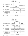
- Fig. 3A is a diagram for explaining the operation of the lighting/light-out control system according to the first example.
- a light-out control signal for giving an instruction for turning OFF the LED 15 is transmitted to the CPU 6.
- the CPU 6 is maintained in a stopping state ((B) in Fig. 3A ) and the CPU program processing has not been started yet ((C) in Fig. 3A ).
- a signal output from the lighting/light-out maintaining circuit 21 has a low (Low) level ((D) in Fig. 3A ).
- the NPN transistor 22 is set into an OFF state and the PMOS transistor 23 is also set into the OFF state.
- the LED 15 is set into the light-out state ((E) in Fig. 3A ).
- the controlling source voltage Vcc is supplied from the control power generating circuit 5 to the CPU 6.
- the driving operation of the CPU 6 is started after a passage of a first time t1 from the supply of the controlling source voltage Vcc to a power-ON reset of the CPU 6 ((B) in Fig. 3A ).
- the lighting/light-out program processing of the CPU 6 is started after a passage of a second time t2 for the initialization of the CPU 6 ((C) in Fig. 3A ).
- a time T1 in Fig. 3A is obtained by adding the power-ON reset time (the first time t1) to the initializing time (the second time t2) and is the time from the supply of the battery voltage to the CPU 6 to the transmission of the switch control signal to the switch driving portion 7. Even if the battery voltage is supplied, a signal output from the lighting/light-out maintaining circuit 21 ("a" point) is maintained to have the low level until the switch control signal is output from the CPU 6.
- Fig. 3B is a diagram for explaining an operation of the lighting/light-out control system according to the second example.
- the CPU 6 is set into a driving state while it is normally operated ((B) in Fig. 3B ), and the lighting/light-out program processing of the CPU 6 is started ((C) in Fig. 3B ).
- the signal output from the lighting/light-out maintaining circuit 21 has a high (High) level ((D) in Fig. 3B ).
- the NPN transistor 22 is set into the ON state and the PMOS transistor 23 is also set into the ON state.
- the LED 15 is set into the lighting state ((E) in Fig. 3B ).
- the control power generating circuit 5 stops the supply of the controlling source voltage Vcc to the CPU 6 so that the driving operation of the CPU 6 is stopped ((B) in Fig. 3B ).
- the driving operation of the CPU 6 is started ((B) in Fig. 3B ).
- a non-processing state is brought for a time (a first time t3) from the stopping state of the CPU 6 to the driving state thereof and is further maintained continuously until a time (a second time t4) for the initialization of the CPU 6 after the first time t3 passes ((C) in Fig. 3B ).
- the battery voltage is always supplied to the control power generating circuit 5 for the first time t3 according to the second example. Therefore, a state of the power-ON reset is no different from the first example.
- a time T2 in Fig. 3B is obtained by adding the first time t3 to the second time t4 and is a time until the CPU 6 is brought into the stopping state and the program processing of the CPU 6 is then started, and the switch control signal is thereafter transmitted.
- a time constant based on the resistor R1 and the capacitor C1 in the lighting/light-out maintaining circuit 21 is set to be equal to or greater than the time T2. In other words, when the program processing of the CPU 6 is started, the output of the CPU 6 has priority over the output of the lighting/light-out maintaining circuit 21.
- the high level signal input as the switch control signal is exactly held for the signal output from the lighting/light-out maintaining circuit 21 during a passage of the time T2, and is then transmitted to the NPN transistor 22 ((D) in Fig. 3B ). Accordingly, the lighting/light-out maintaining circuit 21 functions as a time constant circuit for delaying, by the time T2, the input signal in the driving state brought before the driving operation of the CPU 6 is set into the stopping state and outputting the delayed signal.
- the ON state of the NPN transistor 22 is continuously maintained.
- the ON state of the PMOS transistor 23 is continuously maintained.
- the lighting state of the LED 15 is continuously maintained ((E) in Fig. 3B ).
- the LED 15 is set into the light-out state before an abnormality occurs, the light-out state is continuously maintained.
- FIG. 4 is a diagram showing a structure of a switch driving portion 7A of the lighting/light-out control system according to the second exemplary embodiment.
- the switch driving portions 7A, 7A and 7A have the same structures and include lighting/light-out maintaining circuits 31, 31 and 31, NPN transistors 32, 32 and 32, and NPN transistors 33, 33 and 33 respectively as shown in Fig. 4 .
- the lighting/light-out maintaining circuit 31 has a structure in which a resistor R6 and a capacitor C2 are connected in series between a node "a" and a DC power supply Vcc.
- the NPN transistor 32 has a base connected to the lighting/light-out maintaining circuit 31 through a resistor R7.
- the NPN transistor 32 has a collector connected to a base of the NPN transistor 33.
- PMOS transistors 34, 34 and 34 are used for the switch portions SW2, SW2 and SW2, respectively.
- a gate of the PMOS transistor 34 is connected to a collector of the NPN transistor 33 through a resistor R12.
- the operation of the lighting/light-out control system according to the second exemplary embodiment includes a first example in which a CPU 6 carries out a lighting/light-out control to continuously maintain a light-out state of an LED 15 for a predetermined time in a supply of a battery voltage, and a second example in which the CPU 6 carries out the lighting/light-out control to continuously maintain the lighting state or the light-out state of the LED 15 for a predetermined time.
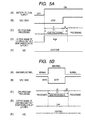
- Fig. 5A is a diagram for explaining the operation of the lighting/light-out control system according to the first example.
- a light-out control signal for giving an instruction for turning OFF the LED 15 is transmitted to the CPU 6.
- the CPU 6 is maintained in a stopping state ((B) in Fig. 5A ) and the CPU program processing has not been started yet ((C) in Fig. 5A ).
- a signal output from the lighting/light-out maintaining circuit 31 has a low (Low) level ((D) in Fig. 5A ).
- the NPN transistors 32 and 33 are set into an OFF state and the PMOS transistor 34 is also set into the OFF state.
- the LED 15 is set into the light-out state ((E) in Fig. 5A ).
- the controlling source voltage Vcc is supplied from a control power generating circuit 5 to the CPU 6 and the lighting/light-out maintaining circuit 31.
- the driving operation of the CPU 6 is started after a passage of a first time t1 from the supply of the controlling source voltage Vcc to a power-ON reset of the CPU 6 ((B) in Fig. 5A ).
- the lighting/light-out program processing of the CPU 6 is started after a passage of a second time t2 for the initialization of the CPU 6 ((C) in Fig. 5A ).
- a time T1 in Fig. 5A is obtained by adding the first time t1 to the second time t2 in the same manner as in the first example of the first exemplary embodiment, and is a time from the supply of the battery voltage to the CPU 6 to the transmission of the switch control signal to the switch driving portion 7A.
- a time constant based on the resistor R6 and the capacitor C2 in the lighting/light-out maintaining circuit 31 is set to be equal to or greater than the time T1.
- the signal output from the lighting/light-out maintaining circuit 31 is changed from the low level signal into the high level signal, and the high level signal is exactly held and is transmitted to the NPN transistor 32 till a passage of the time T1. Accordingly, the signal output from the lighting/light-out maintaining circuit 31 (the output signal on the node "a" point) is set to be the high level signal because the controlling source voltage Vcc is supplied to the lighting/light-out maintaining circuit 31 synchronously with the battery voltage during the passage of the time T1, and the lighting/light-out maintaining circuit 31 functions as a time constant circuit for delaying the high level signal by the time T1 and outputting the delayed signal.
- the ON state of the NPN transistor 32 is continuously maintained.
- the low level signal is input to the base of the NPN transistor 33 so that the NPN transistor 33 is brought into the OFF state. For this reason, the OFF state of the PMOS transistor 34 is continuously maintained. Therefore, the light-out state of the LED 15 is continuously maintained ((E) in Fig. 5A ).
- the program processing of the CPU 6 is started after a passage of the time T1, the output of the CPU 6 has priority over the output of the lighting/light-out maintaining circuit 31 ((E) in Fig. 5A ).
- Fig. 5B is a diagram for explaining an operation of the lighting/light-out control system according to the second example.
- the CPU 6 is set into a driving state while it is normally operated ((B) in Fig. 5B ), and the CPU program processing is started ((C) in Fig. 5B ).
- the signal output from the lighting/light-out maintaining circuit 31 has a low level ((D) in Fig. 5B ).
- the NPN transistor 32 is set into the OFF state
- the NPN transistor 33 is set into the ON state
- the PMOS transistor 34 is also set into the ON state.
- the LED 15 is set into the lighting state ((E) in Fig. 5B ).
- the control power generating circuit 5 stops the supply of the controlling source voltage Vcc to the CPU 6 so that the driving operation of the CPU 6 is stopped ((B) in Fig. 5B ).
- the driving operation of the CPU 6 is started ((B) in Fig. 5B ).
- a non-processing state is brought for a time (a first time t3) from the stopping state of the CPU 6 to the driving state thereof and is further maintained continuously until a time (a second time t4) for the initialization of the CPU 6 after a passage of the first time t3 passes ((C) in Fig. 5B ).
- the battery voltage is always supplied to the control power generating circuit 5 for the first time t3 according to the second example. Therefore, a state of the power-ON reset is brought differently from the first example.
- a time T2 in Fig. 5B is obtained by adding the first time t3 to the second time t4 and is a time until the CPU 6 is brought into the stopping state and the program processing of the CPU 6 is then started, and the switch control signal is thereafter transmitted.
- a time constant based on the resistor R6 and the capacitor C2 in the lighting/light-out maintaining circuit 31 is set to be equal to or greater than the time T2. In other words, when the program processing of the CPU 6 is started, the output of the CPU 6 has priority over the output of the lighting/light-out maintaining circuit 31.
- the low level signal input as the switch control signal is exactly held for the signal output from the lighting/light-out maintaining circuit 31 during a passage of the time T2, and is transmitted to the NPN transistor 32 ((D) in Fig. 5B ). Accordingly, the lighting/light-out maintaining circuit 31 functions as a time constant circuit for delaying, by the time T2, the input signal in the driving state brought before the driving operation of the CPU 6 is set into the stopping state and outputting the delayed signal.
- the OFF state of the NPN transistor 32 is continuously maintained and the ON state of the NPN transistor 33 is continuously maintained.
- the ON state of the PMOS transistor 34 is also maintained continuously. Accordingly, the lighting state of the LED 15 is continuously maintained ((E) in Fig. 5B ). To the contrary, if the LED 15 is set into the light-out state before an abnormality occurs, the light-out state is maintained continuously.
Landscapes
- Engineering & Computer Science (AREA)
- Mechanical Engineering (AREA)
- Lighting Device Outwards From Vehicle And Optical Signal (AREA)
- Circuit Arrangement For Electric Light Sources In General (AREA)
Abstract
Description
- The present disclosure relates to a light source switching (lighting/light-out) control system of a lighting device for a vehicle and more particularly to a lighting/light-out control system of a lighting device for a vehicle which includes a light source unit having a semiconductor light source and a control unit for controlling the light source unit.
- In general, a lighting/light-out control system of a lighting device for a vehicle is constituted to include a plurality of light source units having semiconductor light sources respectively, and a control unit connected to the light source units through feeding lines respectively.
- The control unit has a plurality of switching portions connected in series to the light source units. The switching portions serve to control the semiconductor light sources respectively. The control unit also includes, a plurality of switching driving portions for turning ON/OFF the switching portions respectively, and a control portion for transmitting a switch control signal upon receipt of a lighting/light-out control signal, thereby controlling each of the switch driving portions. A control power generating circuit for generating and supplying a source voltage to the control portion is connected to a front stage of the switch portion (for example, see Japanese Publication
JP-A-2006-73400 - When a battery voltage supplied from the battery power supply is applied (supplied), the control power generating circuit supplies a controlling source voltage to the control portion. The control portion starts a driving operation and transmits a switch control signal for controlling each switch driving portion upon receipt of a lighting/light-out control signal for giving an instruction for turning ON/OFF each semiconductor light source.
- When the battery voltage is supplied, there is started a processing of a lighting/light-out program for a lighting/light-out control to be carried out by the control portion over each semiconductor light source after a passage of several tens of milliseconds after the supply. A delay of several tens of milliseconds is caused by a time taken for power-ON reset which is carried out in the control power generating circuit and the control portion or a time taken for an initialization in the control portion. The time taken for the power-ON reset or the time taken for the initialization in the control portion is needed for the driving operation of the control portion.
- In a lighting/light-out control system having a circuit structure in which a switch driving portion turns ON a switching portion within the delay time, for example, a structure in which a circuit for forcibly supplying a battery voltage is disposed between a control portion and the switch driving portion. For example, in a case in which a turn signal lamp is to be brought into a lighting state to maintain a low beam amplifier into a light-out state, the switch driving portion turns ON the switch portion within the delay time so that the low beam lamp is turned ON.
- In this case, therefore, the low beam lamp is once turned ON immediately after the supply of the battery voltage and is then turned OFF in accordance with the program processing of the control portion. Thus, the semiconductor light source to originally continue (maintain) the light-out state is brought into the lighting state from a stoppage of the driving operation of the control portion to a start of the driving operation. For this reason, there is a problem in that a safety of an operation of a vehicle is decreased.
- In the case in which the program processing is not appropriately carried out so that an abnormality occurs in the control portion, moreover, the driving operation of the control portion is once stopped and is then started after a passage of a predetermined time. In the case in which the abnormality occurs in the control portion when the semiconductor light source is set into the lighting state, accordingly, the semiconductor light source is brought into the light-out state while the driving operation of the control portion is stopped and the control portion is then recovered into a normal state, and the driving operation is thereafter started. Thus, the semiconductor light source to originally continue the lighting state is temporarily brought into the light-out state. For this reason, there is a problem in that the safety in the operation of the vehicle is decreased.
- Therefore, it is an object of the invention to maintain a lighting/light-out state before a stoppage of a driving operation of a control portion, thereby enhancing safety in an operation of a vehicle from the stoppage of the driving operation to a start of the driving operation.
- A lighting/light-out control system of a lighting device for a vehicle, according to an illustrative aspect of the invention, comprises:
- a plurality of semiconductor light sources; and
- a control unit connected to the semiconductor light sources,
- wherein the control unit includes:
- a plurality of switch portions connected to the semiconductor light sources and serving to control the semiconductor light sources respectively;
- a plurality of switch driving portions for turning ON/OFF the switch portions respectively; and
- a control portion for transmitting a switch control signal upon receipt of a lighting/light-out control signal, thereby controlling each of the switch driving portions,
- each of the switch driving portions having a lighting/light-out maintaining circuit for maintaining an ON/OFF state of each of the switch portions, for a predetermined time, in a state brought immediately before a stoppage of a driving operation of the control portion when the driving operation of the control portion is stopped.
- Accordingly, the ON/OFF state of each switch portion is controlled to continue the lighting state or the light-out state before the stoppage of the driving operation of the control portion in a state in which the driving operation is stopped.
- Accordingly, the lighting state or the light-out state before the stoppage of the driving operation can be continuously maintained in the state in which the driving operation of the control portion is stopped. Therefore, it is possible to enhance the safety of the operation of a vehicle.
- In the lighting/light-out control system of a lighting device for a vehicle, the lighting/light-out maintaining circuit controls to maintain light-out of each of the semiconductor light sources while a source voltage is supplied to the control unit and the switch control signal is then transmitted to each of the switch driving portions. Therefore, in the state in which the control portion is stopped during a passage of an initializing time which is needed for the driving operation of the control portion after the supply of the source voltage to the control unit, the switch portion is maintained in the OFF state so that each light source unit can be maintained in the light-out state.
- In the lighting/light-out control system of a lighting device for a vehicle, the lighting/light-out maintaining circuit controls to maintain each of the semiconductor light sources into a state brought immediately before the stoppage of the driving operation of the control portion while the driving operation of the control portion is stopped and the switch control signal is then transmitted to each of the switch driving portions when the driving operation of the control portion is stopped due to an abnormality. Therefore, in the case in which an abnormality occurs in the control portion when the semiconductor light source is set into the lighting state, for example, the light-out state of the semiconductor light source can be maintained continuously.
- In the lighting/light-out control system of a lighting device for a vehicle, the predetermined time for the maintenance of the lighting/light-out maintaining circuit is equal to or longer than a time for stopping the driving operation of the control portion and then transmitting the switching control signal to each of the switch driving portions. Therefore, after the driving operation of the control portion is stopped, it is possible to continuously maintain the state brought immediately before the stoppage of the semiconductor light source.
- In the lighting/light-out control system of a lighting device for a vehicle, the lighting/light-out maintaining circuit is a time constant circuit including a capacitor and a resistor. Therefore, a time for maintaining the state brought immediately before the stoppage of the driving operation of the control portion by the lighting/light-out maintaining circuit can be set by regulating a time constant based on the resistor and the capacitor.
-
-
Fig. 1 is a diagram showing a structure of the lighting/light-out control system of a lighting device for a vehicle according to the first exemplary embodiment of the invention. -
Fig. 2 is a diagram showing a structure of a switch driving portion of the lighting/light-out control system according to the first exemplary embodiment. -
Fig. 3A is a timing diagram for explaining the operation of the lighting/light-out control system according to a first example. -
Fig. 3B is a timing diagram for explaining an operation of the lighting/light-out control system according to a second example. -
Fig. 4 is a diagram showing a structure of aswitch driving portion 7A of the lighting/light-out control system according to the second exemplary embodiment. -
Fig. 5A is a timing diagram for explaining the operation of the lighting/light-out control system according to a first example. -
Fig. 5B is a timing diagram for explaining an operation of the lighting/light-out control system according to a second example. -
- A lighting/light-out control system of a lighting device for a vehicle according to a first exemplary embodiment of the invention will be described below.
Fig. 1 is a diagram showing a structure of the lighting/light-out control system of a lighting device for a vehicle according to the first exemplary embodiment of the invention.Fig. 2 is a diagram showing a structure of a switch driving portion of the lighting/light-out control system according to the first exemplary embodiment. - A lighting/light-out
control system 1 includes acontrol unit 2 and threelight source units control unit 2 is connected to thelight source units control unit 2 includes aninput circuit 4 connected to abattery power supply 8 through a switch portion SW1, a controlpower generating circuit 5 disposed in a rear stage of theinput circuit 4, a CPU (Central Processing Unit) 6 serving as a control portion having an input terminal for inputting a lighting/light-out control signal, switch portions SW2, SW2 and SW2 connected to thelight source units portions CPU 6 respectively. - The
input circuit 4 includes a noise filter and a surge protecting unit (a surge absorber / power zener such as a damping surge). - The control
power generating circuit 5 generates a controlling source voltage Vcc upon receipt of a battery voltage and supplies a power to theCPU 6. - The
switch driving portions circuits NPN transistors Fig. 2 . The lighting/light-out maintainingcircuit 21 has a structure in which a resistor R1 and a capacitor C1 are connected in series between a node "a" and a GND (ground). TheNPN transistor 22 has a base connected to the lighting/light-out maintainingcircuit 21 through a resistor R2. - For example,
PMOS transistors Fig. 2 ). A gate of thePMOS transistor 23 is connected to a collector of theNPN transistor 22 through a resistor R4. - The
light source units regulators control circuits LEDs - An operation of the lighting/light-out control system according to the first exemplary embodiment will be described below.
- The operation of the lighting/light-out control system according to the first exemplary embodiment includes a first example in which the
CPU 6 carries out a lighting/light-out control to continuously maintain a light-out state of theLED 15 for a predetermined time in a supply of a battery voltage and a second example in which theCPU 6 carries out the lighting/light-out control to continuously maintain the lighting or light-out state of theLED 15 for a predetermined time. - The first example will be described below.
Fig. 3A is a diagram for explaining the operation of the lighting/light-out control system according to the first example. - In a state in which the battery voltage is not supplied, a light-out control signal for giving an instruction for turning OFF the
LED 15 is transmitted to theCPU 6. In a state in which the battery voltage is not supplied, accordingly, theCPU 6 is maintained in a stopping state ((B) inFig. 3A ) and the CPU program processing has not been started yet ((C) inFig. 3A ). At this time, a signal output from the lighting/light-out maintainingcircuit 21 has a low (Low) level ((D) inFig. 3A ). In this case, theNPN transistor 22 is set into an OFF state and thePMOS transistor 23 is also set into the OFF state. At this time, theLED 15 is set into the light-out state ((E) inFig. 3A ). - When the battery voltage is supplied ((A) in
Fig. 3A ), the controlling source voltage Vcc is supplied from the controlpower generating circuit 5 to theCPU 6. When the controlling source voltage Vcc is supplied to theCPU 6, the driving operation of theCPU 6 is started after a passage of a first time t1 from the supply of the controlling source voltage Vcc to a power-ON reset of the CPU 6 ((B) inFig. 3A ). Furthermore, the lighting/light-out program processing of theCPU 6 is started after a passage of a second time t2 for the initialization of the CPU 6 ((C) inFig. 3A ). - A time T1 in
Fig. 3A is obtained by adding the power-ON reset time (the first time t1) to the initializing time (the second time t2) and is the time from the supply of the battery voltage to theCPU 6 to the transmission of the switch control signal to theswitch driving portion 7. Even if the battery voltage is supplied, a signal output from the lighting/light-out maintaining circuit 21 ("a" point) is maintained to have the low level until the switch control signal is output from theCPU 6. - As described above, when the low level signal is transmitted from the lighting/light-out maintaining
circuit 21 to theNPN transistor 22, the OFF state of theNPN transistor 22 is continuously maintained. For this reason, the OFF state of thePMOS transistor 23 is continuously maintained. Therefore, the light-out state of theLED 15 is continuously maintained ((E) inFig. 3A ). When the program processing of theCPU 6 is started after a passage of the time T1, the output of theCPU 6 has priority over the output of the lighting/light-out maintaining circuit 21 ((E) inFig. 3A ). - Next, the second example will be described.
Fig. 3B is a diagram for explaining an operation of the lighting/light-out control system according to the second example. - The
CPU 6 is set into a driving state while it is normally operated ((B) inFig. 3B ), and the lighting/light-out program processing of theCPU 6 is started ((C) inFig. 3B ). At this time, the signal output from the lighting/light-out maintainingcircuit 21 has a high (High) level ((D) inFig. 3B ). In this case, theNPN transistor 22 is set into the ON state and thePMOS transistor 23 is also set into the ON state. At this time, theLED 15 is set into the lighting state ((E) inFig. 3B ). - In the case in which an abnormality then occurs in the CPU 6 ((A) in
Fig. 3B ), the controlpower generating circuit 5 stops the supply of the controlling source voltage Vcc to theCPU 6 so that the driving operation of theCPU 6 is stopped ((B) inFig. 3B ). When theCPU 6 is thereafter recovered from the abnormal state to the normal state, the driving operation of theCPU 6 is started ((B) inFig. 3B ). - In the lighting/light-out program processing of the
CPU 6, a non-processing state is brought for a time (a first time t3) from the stopping state of theCPU 6 to the driving state thereof and is further maintained continuously until a time (a second time t4) for the initialization of theCPU 6 after the first time t3 passes ((C) inFig. 3B ). The battery voltage is always supplied to the controlpower generating circuit 5 for the first time t3 according to the second example. Therefore, a state of the power-ON reset is no different from the first example. - A time T2 in
Fig. 3B is obtained by adding the first time t3 to the second time t4 and is a time until theCPU 6 is brought into the stopping state and the program processing of theCPU 6 is then started, and the switch control signal is thereafter transmitted. A time constant based on the resistor R1 and the capacitor C1 in the lighting/light-out maintainingcircuit 21 is set to be equal to or greater than the time T2. In other words, when the program processing of theCPU 6 is started, the output of theCPU 6 has priority over the output of the lighting/light-out maintainingcircuit 21. - When the
CPU 6 is brought from the driving state into the stopping state, the high level signal input as the switch control signal is exactly held for the signal output from the lighting/light-out maintainingcircuit 21 during a passage of the time T2, and is then transmitted to the NPN transistor 22 ((D) inFig. 3B ). Accordingly, the lighting/light-out maintainingcircuit 21 functions as a time constant circuit for delaying, by the time T2, the input signal in the driving state brought before the driving operation of theCPU 6 is set into the stopping state and outputting the delayed signal. - As described above, when the high level signal is transmitted from the lighting/light-out maintaining
circuit 21 to the NPN transistor 22 ((D) inFig. 3B ), the ON state of theNPN transistor 22 is continuously maintained. For this reason, the ON state of thePMOS transistor 23 is continuously maintained. Accordingly, the lighting state of theLED 15 is continuously maintained ((E) inFig. 3B ). To the contrary, if theLED 15 is set into the light-out state before an abnormality occurs, the light-out state is continuously maintained. - A lighting/light-out control system of a lighting device for a vehicle according to a second exemplary embodiment will be described below. The second exemplary embodiment is different from the first exemplary embodiment in respect of only a circuit structure of a switch driving portion. In the following description of the second exemplary embodiment, therefore, the same portions as those in the first exemplary embodiment will be briefly explained.
Fig. 4 is a diagram showing a structure of aswitch driving portion 7A of the lighting/light-out control system according to the second exemplary embodiment. - The
switch driving portions circuits NPN transistors NPN transistors Fig. 4 . The lighting/light-out maintainingcircuit 31 has a structure in which a resistor R6 and a capacitor C2 are connected in series between a node "a" and a DC power supply Vcc. TheNPN transistor 32 has a base connected to the lighting/light-out maintainingcircuit 31 through a resistor R7. TheNPN transistor 32 has a collector connected to a base of theNPN transistor 33. - For example,
PMOS transistors PMOS transistor 34 is connected to a collector of theNPN transistor 33 through a resistor R12. - An operation of the lighting/light-out control system according to the second exemplary embodiment will be described below. The operation of the lighting/light-out control system according to the second exemplary embodiment includes a first example in which a
CPU 6 carries out a lighting/light-out control to continuously maintain a light-out state of anLED 15 for a predetermined time in a supply of a battery voltage, and a second example in which theCPU 6 carries out the lighting/light-out control to continuously maintain the lighting state or the light-out state of theLED 15 for a predetermined time. - The first example will be described below.
Fig. 5A is a diagram for explaining the operation of the lighting/light-out control system according to the first example. - In a state in which the battery voltage is not supplied, a light-out control signal for giving an instruction for turning OFF the
LED 15 is transmitted to theCPU 6. In a state in which the battery voltage is not supplied, accordingly, theCPU 6 is maintained in a stopping state ((B) inFig. 5A ) and the CPU program processing has not been started yet ((C) inFig. 5A ). At this time, a signal output from the lighting/light-out maintainingcircuit 31 has a low (Low) level ((D) inFig. 5A ). In this case, theNPN transistors PMOS transistor 34 is also set into the OFF state. At this time, theLED 15 is set into the light-out state ((E) inFig. 5A ). - When the battery voltage is supplied ((A) in
Fig. 5A ), the controlling source voltage Vcc is supplied from a controlpower generating circuit 5 to theCPU 6 and the lighting/light-out maintainingcircuit 31. When the controlling source voltage Vcc is supplied to the lighting/light-out maintainingcircuit 31, the driving operation of theCPU 6 is started after a passage of a first time t1 from the supply of the controlling source voltage Vcc to a power-ON reset of the CPU 6 ((B) inFig. 5A ). Furthermore, the lighting/light-out program processing of theCPU 6 is started after a passage of a second time t2 for the initialization of the CPU 6 ((C) inFig. 5A ). - A time T1 in
Fig. 5A is obtained by adding the first time t1 to the second time t2 in the same manner as in the first example of the first exemplary embodiment, and is a time from the supply of the battery voltage to theCPU 6 to the transmission of the switch control signal to theswitch driving portion 7A. A time constant based on the resistor R6 and the capacitor C2 in the lighting/light-out maintainingcircuit 31 is set to be equal to or greater than the time T1. - As described above, when the battery voltage is supplied, the signal output from the lighting/light-out maintaining
circuit 31 is changed from the low level signal into the high level signal, and the high level signal is exactly held and is transmitted to theNPN transistor 32 till a passage of the time T1. Accordingly, the signal output from the lighting/light-out maintaining circuit 31 (the output signal on the node "a" point) is set to be the high level signal because the controlling source voltage Vcc is supplied to the lighting/light-out maintainingcircuit 31 synchronously with the battery voltage during the passage of the time T1, and the lighting/light-out maintainingcircuit 31 functions as a time constant circuit for delaying the high level signal by the time T1 and outputting the delayed signal. - As described above, when the high level signal is transmitted from the lighting/light-out maintaining
circuit 31 to theNPN transistor 32, the ON state of theNPN transistor 32 is continuously maintained. The low level signal is input to the base of theNPN transistor 33 so that theNPN transistor 33 is brought into the OFF state. For this reason, the OFF state of thePMOS transistor 34 is continuously maintained. Therefore, the light-out state of theLED 15 is continuously maintained ((E) inFig. 5A ). When the program processing of theCPU 6 is started after a passage of the time T1, the output of theCPU 6 has priority over the output of the lighting/light-out maintaining circuit 31 ((E) inFig. 5A ). - Next, the second example will be described.
Fig. 5B is a diagram for explaining an operation of the lighting/light-out control system according to the second example. - The
CPU 6 is set into a driving state while it is normally operated ((B) inFig. 5B ), and the CPU program processing is started ((C) inFig. 5B ). At this time, the signal output from the lighting/light-out maintainingcircuit 31 has a low level ((D) inFig. 5B ). In this case, theNPN transistor 32 is set into the OFF state, theNPN transistor 33 is set into the ON state, and thePMOS transistor 34 is also set into the ON state. At this time, theLED 15 is set into the lighting state ((E) inFig. 5B ). - In the case in which an abnormality then occurs in the CPU 6 ((A) in
Fig. 5B ), the controlpower generating circuit 5 stops the supply of the controlling source voltage Vcc to theCPU 6 so that the driving operation of theCPU 6 is stopped ((B) inFig. 5B ). When theCPU 6 is thereafter recovered from the abnormal state to the normal state, the driving operation of theCPU 6 is started ((B) inFig. 5B ). - In the lighting/light-out program processing of the
CPU 6, a non-processing state is brought for a time (a first time t3) from the stopping state of theCPU 6 to the driving state thereof and is further maintained continuously until a time (a second time t4) for the initialization of theCPU 6 after a passage of the first time t3 passes ((C) inFig. 5B ). The battery voltage is always supplied to the controlpower generating circuit 5 for the first time t3 according to the second example. Therefore, a state of the power-ON reset is brought differently from the first example. - A time T2 in
Fig. 5B is obtained by adding the first time t3 to the second time t4 and is a time until theCPU 6 is brought into the stopping state and the program processing of theCPU 6 is then started, and the switch control signal is thereafter transmitted. A time constant based on the resistor R6 and the capacitor C2 in the lighting/light-out maintainingcircuit 31 is set to be equal to or greater than the time T2. In other words, when the program processing of theCPU 6 is started, the output of theCPU 6 has priority over the output of the lighting/light-out maintainingcircuit 31. - When the
CPU 6 is brought from the driving state into the stopping state, the low level signal input as the switch control signal is exactly held for the signal output from the lighting/light-out maintainingcircuit 31 during a passage of the time T2, and is transmitted to the NPN transistor 32 ((D) inFig. 5B ). Accordingly, the lighting/light-out maintainingcircuit 31 functions as a time constant circuit for delaying, by the time T2, the input signal in the driving state brought before the driving operation of theCPU 6 is set into the stopping state and outputting the delayed signal. - As described above, when the low level signal is transmitted from the lighting/light-out maintaining
circuit 31 to the NPN transistor 32 ((D) inFig. 5B ), the OFF state of theNPN transistor 32 is continuously maintained and the ON state of theNPN transistor 33 is continuously maintained. For this reason, the ON state of thePMOS transistor 34 is also maintained continuously. Accordingly, the lighting state of theLED 15 is continuously maintained ((E) inFig. 5B ). To the contrary, if theLED 15 is set into the light-out state before an abnormality occurs, the light-out state is maintained continuously. - Each of the exemplary embodiments is only illustrative as a suitable embodiment of the invention and the invention can be variously changed and executed without departing from the scope thereof.
Claims (5)
- A lighting/light-out control system of a lighting device for a vehicle, the lighting/light-out control system comprising:a plurality of semiconductor light sources; anda control unit connected to the semiconductor light sources,wherein the control unit includes:a plurality of switch portions connected to the semiconductor light sources and serving to control the semiconductor light sources respectively;a plurality of switch driving portions for turning ON/OFF the switch portions respectively; anda control portion for transmitting a switch control signal upon receipt of a lighting/light-out control signal, thereby controlling each of the switch driving portions,each of the switch driving portions having a lighting/light-out maintaining circuit for maintaining an ON/OFF state of each of the switch portions, for a predetermined time, in a state brought immediately before a stoppage of a driving operation of the control portion when the driving operation of the control portion is stopped.
- The lighting/light-out control system of a lighting device for a vehicle according to claim 1, wherein the lighting/light-out maintaining circuit controls to maintain light-out of each of the semiconductor light sources while a source voltage is supplied to the control unit and, thereafter, the switch control signal is transmitted to each of the switch driving portions.
- The lighting/light-out control system of a lighting device for a vehicle according to claim 1, wherein the lighting/light-out maintaining circuit controls to maintain each of the semiconductor light sources in a state brought immediately before the stoppage of the driving operation of the control portion while the driving operation of the control portion is stopped and, thereafter, the switch control signal is transmitted to each of the switch driving portions when the driving operation of the control portion is stopped due to an abnormality.
- The lighting/light-out control system of a lighting device for a vehicle according to claim 3, wherein the predetermined time for the maintenance of the lighting/light-out maintaining circuit is equal to or longer than a time for stopping the driving operation of the control portion and then transmitting the switching control signal to each of the switch driving portions.
- The lighting/light-out control system of a lighting device for a vehicle according to claim 1, wherein the lighting/light-out maintaining circuit is a time constant circuit including a capacitor and a resistor.
Applications Claiming Priority (1)
| Application Number | Priority Date | Filing Date | Title |
|---|---|---|---|
| JP2008238142A JP5276939B2 (en) | 2008-09-17 | 2008-09-17 | On / off control system for vehicular lamp |
Publications (2)
| Publication Number | Publication Date |
|---|---|
| EP2170016A1 true EP2170016A1 (en) | 2010-03-31 |
| EP2170016B1 EP2170016B1 (en) | 2018-10-31 |
Family
ID=41506513
Family Applications (1)
| Application Number | Title | Priority Date | Filing Date |
|---|---|---|---|
| EP09011786.2A Not-in-force EP2170016B1 (en) | 2008-09-17 | 2009-09-16 | Light source switching control system of lighting device for vehicle |
Country Status (2)
| Country | Link |
|---|---|
| EP (1) | EP2170016B1 (en) |
| JP (1) | JP5276939B2 (en) |
Cited By (1)
| Publication number | Priority date | Publication date | Assignee | Title |
|---|---|---|---|---|
| EP3127795A4 (en) * | 2014-03-31 | 2018-01-17 | Honda Motor Co., Ltd. | Vehicle led lighting device system |
Citations (7)
| Publication number | Priority date | Publication date | Assignee | Title |
|---|---|---|---|---|
| US5666028A (en) * | 1994-04-06 | 1997-09-09 | Gentex Corporation | Automobile headlamp and running light control system |
| WO1998046051A1 (en) * | 1997-04-10 | 1998-10-15 | Koninklijke Philips Electronics N.V. | Ballast |
| US6005348A (en) | 1996-03-11 | 1999-12-21 | Nissan Motor Co., Ltd. | Circuit keeping daytime head lamps on after engine and head lamp switch are turned off |
| US20030139862A1 (en) * | 2002-01-22 | 2003-07-24 | Yuhki Osada | Display control apparatus for vehicle and the method thereof |
| US20060055244A1 (en) * | 2004-09-03 | 2006-03-16 | Koito Manufacturing Co., Ltd. | Lighting control circuit for vehicle lighting equipment |
| US7106036B1 (en) * | 2004-06-30 | 2006-09-12 | National Semiconductor Corporation | Apparatus and method for high-frequency PWM with soft-start |
| DE102008008836A1 (en) | 2007-02-15 | 2008-08-21 | Koito Mfg. Co., Ltd. | Light emitting means |
Family Cites Families (3)
| Publication number | Priority date | Publication date | Assignee | Title |
|---|---|---|---|---|
| JP2609702B2 (en) * | 1988-10-19 | 1997-05-14 | 日本電気ホームエレクトロニクス株式会社 | Lighting lighting device |
| JPH10222402A (en) * | 1997-02-12 | 1998-08-21 | Nissan Motor Co Ltd | Vehicle control device |
| JP2006172784A (en) * | 2004-12-14 | 2006-06-29 | Koito Mfg Co Ltd | Lighting control circuit for vehicular lamp |
-
2008
- 2008-09-17 JP JP2008238142A patent/JP5276939B2/en not_active Expired - Fee Related
-
2009
- 2009-09-16 EP EP09011786.2A patent/EP2170016B1/en not_active Not-in-force
Patent Citations (7)
| Publication number | Priority date | Publication date | Assignee | Title |
|---|---|---|---|---|
| US5666028A (en) * | 1994-04-06 | 1997-09-09 | Gentex Corporation | Automobile headlamp and running light control system |
| US6005348A (en) | 1996-03-11 | 1999-12-21 | Nissan Motor Co., Ltd. | Circuit keeping daytime head lamps on after engine and head lamp switch are turned off |
| WO1998046051A1 (en) * | 1997-04-10 | 1998-10-15 | Koninklijke Philips Electronics N.V. | Ballast |
| US20030139862A1 (en) * | 2002-01-22 | 2003-07-24 | Yuhki Osada | Display control apparatus for vehicle and the method thereof |
| US7106036B1 (en) * | 2004-06-30 | 2006-09-12 | National Semiconductor Corporation | Apparatus and method for high-frequency PWM with soft-start |
| US20060055244A1 (en) * | 2004-09-03 | 2006-03-16 | Koito Manufacturing Co., Ltd. | Lighting control circuit for vehicle lighting equipment |
| DE102008008836A1 (en) | 2007-02-15 | 2008-08-21 | Koito Mfg. Co., Ltd. | Light emitting means |
Cited By (1)
| Publication number | Priority date | Publication date | Assignee | Title |
|---|---|---|---|---|
| EP3127795A4 (en) * | 2014-03-31 | 2018-01-17 | Honda Motor Co., Ltd. | Vehicle led lighting device system |
Also Published As
| Publication number | Publication date |
|---|---|
| JP2010073423A (en) | 2010-04-02 |
| JP5276939B2 (en) | 2013-08-28 |
| EP2170016B1 (en) | 2018-10-31 |
Similar Documents
| Publication | Publication Date | Title |
|---|---|---|
| EP2019570B1 (en) | Lighting control for vehicle lighting device | |
| US7902773B2 (en) | Light emitting device | |
| US7327051B2 (en) | Lighting control circuit for vehicle lamps | |
| US7403107B2 (en) | Lighting control circuit for vehicle lighting equipment | |
| US9748064B2 (en) | Fail-safe circuit | |
| US9130546B2 (en) | Drive circuit for semiconductor device | |
| US10624172B1 (en) | Short/open protecting circuit and a method thereof | |
| JP2006172784A (en) | Lighting control circuit for vehicular lamp | |
| EP2170016B1 (en) | Light source switching control system of lighting device for vehicle | |
| KR100674873B1 (en) | Time control circuit of backlight inverter | |
| JP6613489B2 (en) | Start-up circuit | |
| JP4430280B2 (en) | Optical transmission equipment | |
| US20050127983A1 (en) | Voltage booster device having voltage-suppressing circuit | |
| KR20170023575A (en) | Aircraft power voltage sensing processing device | |
| US9981595B2 (en) | Vehicle lamp | |
| JP6466761B2 (en) | Semiconductor device and power supply method | |
| JP6191149B2 (en) | LED lighting circuit for vehicle lighting | |
| KR102468993B1 (en) | Apparatus of driving a light source and method thereof | |
| US20110285430A1 (en) | Hot-swap controller | |
| CN115134968B (en) | Electronic system for driving light source and method for driving light source | |
| KR20200069677A (en) | Apparatus for driving warning light and method for driving the same | |
| US20070280313A1 (en) | Method and Apparatus for Driving a Light Emitting Device | |
| US10345832B1 (en) | Insulation system and substrate processing apparatus | |
| JP3755416B2 (en) | Load control device | |
| KR101044725B1 (en) | Voltage regulator power supply switching circuit of the engine control unit |
Legal Events
| Date | Code | Title | Description |
|---|---|---|---|
| PUAI | Public reference made under article 153(3) epc to a published international application that has entered the european phase |
Free format text: ORIGINAL CODE: 0009012 |
|
| 17P | Request for examination filed |
Effective date: 20090916 |
|
| AK | Designated contracting states |
Kind code of ref document: A1 Designated state(s): AT BE BG CH CY CZ DE DK EE ES FI FR GB GR HR HU IE IS IT LI LT LU LV MC MK MT NL NO PL PT RO SE SI SK SM TR |
|
| AX | Request for extension of the european patent |
Extension state: AL BA RS |
|
| 17Q | First examination report despatched |
Effective date: 20110105 |
|
| STAA | Information on the status of an ep patent application or granted ep patent |
Free format text: STATUS: EXAMINATION IS IN PROGRESS |
|
| GRAP | Despatch of communication of intention to grant a patent |
Free format text: ORIGINAL CODE: EPIDOSNIGR1 |
|
| STAA | Information on the status of an ep patent application or granted ep patent |
Free format text: STATUS: GRANT OF PATENT IS INTENDED |
|
| INTG | Intention to grant announced |
Effective date: 20180531 |
|
| GRAS | Grant fee paid |
Free format text: ORIGINAL CODE: EPIDOSNIGR3 |
|
| GRAA | (expected) grant |
Free format text: ORIGINAL CODE: 0009210 |
|
| STAA | Information on the status of an ep patent application or granted ep patent |
Free format text: STATUS: THE PATENT HAS BEEN GRANTED |
|
| AK | Designated contracting states |
Kind code of ref document: B1 Designated state(s): AT BE BG CH CY CZ DE DK EE ES FI FR GB GR HR HU IE IS IT LI LT LU LV MC MK MT NL NO PL PT RO SE SI SK SM TR |
|
| REG | Reference to a national code |
Ref country code: CH Ref legal event code: EP Ref country code: GB Ref legal event code: FG4D |
|
| REG | Reference to a national code |
Ref country code: AT Ref legal event code: REF Ref document number: 1060956 Country of ref document: AT Kind code of ref document: T Effective date: 20181115 |
|
| REG | Reference to a national code |
Ref country code: DE Ref legal event code: R096 Ref document number: 602009055327 Country of ref document: DE |
|
| REG | Reference to a national code |
Ref country code: IE Ref legal event code: FG4D |
|
| REG | Reference to a national code |
Ref country code: NL Ref legal event code: MP Effective date: 20181031 |
|
| REG | Reference to a national code |
Ref country code: LT Ref legal event code: MG4D |
|
| REG | Reference to a national code |
Ref country code: AT Ref legal event code: MK05 Ref document number: 1060956 Country of ref document: AT Kind code of ref document: T Effective date: 20181031 |
|
| PG25 | Lapsed in a contracting state [announced via postgrant information from national office to epo] |
Ref country code: FI Free format text: LAPSE BECAUSE OF FAILURE TO SUBMIT A TRANSLATION OF THE DESCRIPTION OR TO PAY THE FEE WITHIN THE PRESCRIBED TIME-LIMIT Effective date: 20181031 Ref country code: BG Free format text: LAPSE BECAUSE OF FAILURE TO SUBMIT A TRANSLATION OF THE DESCRIPTION OR TO PAY THE FEE WITHIN THE PRESCRIBED TIME-LIMIT Effective date: 20190131 Ref country code: PL Free format text: LAPSE BECAUSE OF FAILURE TO SUBMIT A TRANSLATION OF THE DESCRIPTION OR TO PAY THE FEE WITHIN THE PRESCRIBED TIME-LIMIT Effective date: 20181031 Ref country code: HR Free format text: LAPSE BECAUSE OF FAILURE TO SUBMIT A TRANSLATION OF THE DESCRIPTION OR TO PAY THE FEE WITHIN THE PRESCRIBED TIME-LIMIT Effective date: 20181031 Ref country code: LV Free format text: LAPSE BECAUSE OF FAILURE TO SUBMIT A TRANSLATION OF THE DESCRIPTION OR TO PAY THE FEE WITHIN THE PRESCRIBED TIME-LIMIT Effective date: 20181031 Ref country code: IS Free format text: LAPSE BECAUSE OF FAILURE TO SUBMIT A TRANSLATION OF THE DESCRIPTION OR TO PAY THE FEE WITHIN THE PRESCRIBED TIME-LIMIT Effective date: 20190228 Ref country code: AT Free format text: LAPSE BECAUSE OF FAILURE TO SUBMIT A TRANSLATION OF THE DESCRIPTION OR TO PAY THE FEE WITHIN THE PRESCRIBED TIME-LIMIT Effective date: 20181031 Ref country code: ES Free format text: LAPSE BECAUSE OF FAILURE TO SUBMIT A TRANSLATION OF THE DESCRIPTION OR TO PAY THE FEE WITHIN THE PRESCRIBED TIME-LIMIT Effective date: 20181031 Ref country code: NO Free format text: LAPSE BECAUSE OF FAILURE TO SUBMIT A TRANSLATION OF THE DESCRIPTION OR TO PAY THE FEE WITHIN THE PRESCRIBED TIME-LIMIT Effective date: 20190131 Ref country code: LT Free format text: LAPSE BECAUSE OF FAILURE TO SUBMIT A TRANSLATION OF THE DESCRIPTION OR TO PAY THE FEE WITHIN THE PRESCRIBED TIME-LIMIT Effective date: 20181031 |
|
| PG25 | Lapsed in a contracting state [announced via postgrant information from national office to epo] |
Ref country code: NL Free format text: LAPSE BECAUSE OF FAILURE TO SUBMIT A TRANSLATION OF THE DESCRIPTION OR TO PAY THE FEE WITHIN THE PRESCRIBED TIME-LIMIT Effective date: 20181031 Ref country code: PT Free format text: LAPSE BECAUSE OF FAILURE TO SUBMIT A TRANSLATION OF THE DESCRIPTION OR TO PAY THE FEE WITHIN THE PRESCRIBED TIME-LIMIT Effective date: 20190301 Ref country code: GR Free format text: LAPSE BECAUSE OF FAILURE TO SUBMIT A TRANSLATION OF THE DESCRIPTION OR TO PAY THE FEE WITHIN THE PRESCRIBED TIME-LIMIT Effective date: 20190201 Ref country code: SE Free format text: LAPSE BECAUSE OF FAILURE TO SUBMIT A TRANSLATION OF THE DESCRIPTION OR TO PAY THE FEE WITHIN THE PRESCRIBED TIME-LIMIT Effective date: 20181031 |
|
| PG25 | Lapsed in a contracting state [announced via postgrant information from national office to epo] |
Ref country code: IT Free format text: LAPSE BECAUSE OF FAILURE TO SUBMIT A TRANSLATION OF THE DESCRIPTION OR TO PAY THE FEE WITHIN THE PRESCRIBED TIME-LIMIT Effective date: 20181031 Ref country code: CZ Free format text: LAPSE BECAUSE OF FAILURE TO SUBMIT A TRANSLATION OF THE DESCRIPTION OR TO PAY THE FEE WITHIN THE PRESCRIBED TIME-LIMIT Effective date: 20181031 Ref country code: DK Free format text: LAPSE BECAUSE OF FAILURE TO SUBMIT A TRANSLATION OF THE DESCRIPTION OR TO PAY THE FEE WITHIN THE PRESCRIBED TIME-LIMIT Effective date: 20181031 |
|
| REG | Reference to a national code |
Ref country code: DE Ref legal event code: R097 Ref document number: 602009055327 Country of ref document: DE |
|
| PG25 | Lapsed in a contracting state [announced via postgrant information from national office to epo] |
Ref country code: EE Free format text: LAPSE BECAUSE OF FAILURE TO SUBMIT A TRANSLATION OF THE DESCRIPTION OR TO PAY THE FEE WITHIN THE PRESCRIBED TIME-LIMIT Effective date: 20181031 Ref country code: SM Free format text: LAPSE BECAUSE OF FAILURE TO SUBMIT A TRANSLATION OF THE DESCRIPTION OR TO PAY THE FEE WITHIN THE PRESCRIBED TIME-LIMIT Effective date: 20181031 Ref country code: SK Free format text: LAPSE BECAUSE OF FAILURE TO SUBMIT A TRANSLATION OF THE DESCRIPTION OR TO PAY THE FEE WITHIN THE PRESCRIBED TIME-LIMIT Effective date: 20181031 Ref country code: RO Free format text: LAPSE BECAUSE OF FAILURE TO SUBMIT A TRANSLATION OF THE DESCRIPTION OR TO PAY THE FEE WITHIN THE PRESCRIBED TIME-LIMIT Effective date: 20181031 |
|
| PLBE | No opposition filed within time limit |
Free format text: ORIGINAL CODE: 0009261 |
|
| STAA | Information on the status of an ep patent application or granted ep patent |
Free format text: STATUS: NO OPPOSITION FILED WITHIN TIME LIMIT |
|
| 26N | No opposition filed |
Effective date: 20190801 |
|
| PG25 | Lapsed in a contracting state [announced via postgrant information from national office to epo] |
Ref country code: SI Free format text: LAPSE BECAUSE OF FAILURE TO SUBMIT A TRANSLATION OF THE DESCRIPTION OR TO PAY THE FEE WITHIN THE PRESCRIBED TIME-LIMIT Effective date: 20181031 |
|
| PGFP | Annual fee paid to national office [announced via postgrant information from national office to epo] |
Ref country code: FR Payment date: 20190815 Year of fee payment: 11 Ref country code: DE Payment date: 20190903 Year of fee payment: 11 |
|
| PG25 | Lapsed in a contracting state [announced via postgrant information from national office to epo] |
Ref country code: TR Free format text: LAPSE BECAUSE OF FAILURE TO SUBMIT A TRANSLATION OF THE DESCRIPTION OR TO PAY THE FEE WITHIN THE PRESCRIBED TIME-LIMIT Effective date: 20181031 |
|
| PG25 | Lapsed in a contracting state [announced via postgrant information from national office to epo] |
Ref country code: MC Free format text: LAPSE BECAUSE OF FAILURE TO SUBMIT A TRANSLATION OF THE DESCRIPTION OR TO PAY THE FEE WITHIN THE PRESCRIBED TIME-LIMIT Effective date: 20181031 |
|
| REG | Reference to a national code |
Ref country code: CH Ref legal event code: PL |
|
| PG25 | Lapsed in a contracting state [announced via postgrant information from national office to epo] |
Ref country code: CH Free format text: LAPSE BECAUSE OF NON-PAYMENT OF DUE FEES Effective date: 20190930 Ref country code: LI Free format text: LAPSE BECAUSE OF NON-PAYMENT OF DUE FEES Effective date: 20190930 Ref country code: IE Free format text: LAPSE BECAUSE OF NON-PAYMENT OF DUE FEES Effective date: 20190916 Ref country code: LU Free format text: LAPSE BECAUSE OF NON-PAYMENT OF DUE FEES Effective date: 20190916 |
|
| REG | Reference to a national code |
Ref country code: BE Ref legal event code: MM Effective date: 20190930 |
|
| PG25 | Lapsed in a contracting state [announced via postgrant information from national office to epo] |
Ref country code: BE Free format text: LAPSE BECAUSE OF NON-PAYMENT OF DUE FEES Effective date: 20190930 |
|
| GBPC | Gb: european patent ceased through non-payment of renewal fee |
Effective date: 20190916 |
|
| PG25 | Lapsed in a contracting state [announced via postgrant information from national office to epo] |
Ref country code: GB Free format text: LAPSE BECAUSE OF NON-PAYMENT OF DUE FEES Effective date: 20190916 |
|
| REG | Reference to a national code |
Ref country code: DE Ref legal event code: R119 Ref document number: 602009055327 Country of ref document: DE |
|
| PG25 | Lapsed in a contracting state [announced via postgrant information from national office to epo] |
Ref country code: CY Free format text: LAPSE BECAUSE OF FAILURE TO SUBMIT A TRANSLATION OF THE DESCRIPTION OR TO PAY THE FEE WITHIN THE PRESCRIBED TIME-LIMIT Effective date: 20181031 |
|
| PG25 | Lapsed in a contracting state [announced via postgrant information from national office to epo] |
Ref country code: DE Free format text: LAPSE BECAUSE OF NON-PAYMENT OF DUE FEES Effective date: 20210401 Ref country code: HU Free format text: LAPSE BECAUSE OF FAILURE TO SUBMIT A TRANSLATION OF THE DESCRIPTION OR TO PAY THE FEE WITHIN THE PRESCRIBED TIME-LIMIT; INVALID AB INITIO Effective date: 20090916 Ref country code: FR Free format text: LAPSE BECAUSE OF NON-PAYMENT OF DUE FEES Effective date: 20200930 Ref country code: MT Free format text: LAPSE BECAUSE OF FAILURE TO SUBMIT A TRANSLATION OF THE DESCRIPTION OR TO PAY THE FEE WITHIN THE PRESCRIBED TIME-LIMIT Effective date: 20181031 |
|
| PG25 | Lapsed in a contracting state [announced via postgrant information from national office to epo] |
Ref country code: MK Free format text: LAPSE BECAUSE OF FAILURE TO SUBMIT A TRANSLATION OF THE DESCRIPTION OR TO PAY THE FEE WITHIN THE PRESCRIBED TIME-LIMIT Effective date: 20181031 |