EP2169798A2 - Self Powered Electronic Overload Method and System - Google Patents
Self Powered Electronic Overload Method and System Download PDFInfo
- Publication number
- EP2169798A2 EP2169798A2 EP09171779A EP09171779A EP2169798A2 EP 2169798 A2 EP2169798 A2 EP 2169798A2 EP 09171779 A EP09171779 A EP 09171779A EP 09171779 A EP09171779 A EP 09171779A EP 2169798 A2 EP2169798 A2 EP 2169798A2
- Authority
- EP
- European Patent Office
- Prior art keywords
- power supply
- power
- processor
- circuit
- current
- Prior art date
- Legal status (The legal status is an assumption and is not a legal conclusion. Google has not performed a legal analysis and makes no representation as to the accuracy of the status listed.)
- Granted
Links
Images

Classifications
-
- H—ELECTRICITY
- H02—GENERATION; CONVERSION OR DISTRIBUTION OF ELECTRIC POWER
- H02H—EMERGENCY PROTECTIVE CIRCUIT ARRANGEMENTS
- H02H1/00—Details of emergency protective circuit arrangements
- H02H1/06—Arrangements for supplying operative power
Definitions
- the present invention relates generally to protective circuitry, such as overload circuits. More particularly, the invention relates to a processor-based overload relay that is self-powered by virtue of power management components, permitting power to be stored for its operation, while performing measurements of voltage and current.
- Overload relays and similar circuits are used in a wide range of settings.
- a motor starter or motor controller is typically coupled to a motor to supply single or three-phase power.
- the motor drive in many applications, may synthesize an output waveform to vary the frequency of the drive power so as to permit the motor to be driven at various speeds. The waveform may also be manipulated to control torque, and so forth.
- Motor controllers do not typically provide for interrupting power to the motor in case of need.
- other protective devices typically serve this purpose. Such devices may include fuses that are often positioned upstream of all other circuitry and downstream of a power supply, such as the electric power grid. The fuses may be supplemented by magnetic and thermal overload circuitry. Magnetic overload circuitry typically trips to open the power circuit in response to rapid changes in current. Other overload circuitry may operate more slowly, and may model motor windings or other wiring, to permit opening of the circuitry should longer-term rises in temperature be detected or estimated.
- Such relays can be vary from quite simple electro-mechanical devices to more sophisticated circuitry that incorporates application specific integrated circuits (ASICs), or processors, typically microprocessors.
- ASICs and processors offer a significant benefit in being capable of analyzing current and voltage data and judiciously opening or closing power circuits based upon the analysis.
- sophisticated yet high production (and thus cost effective) processors including microprocessors and field programmable gate arrays may be used for such purposes.
- the present invention provides novel circuitry that can be used in overload relays and similar devices configured to respond to such needs.
- the circuitry may be used in a wide range of settings, but is particularly well-suited to devices where currents and/or voltages are measured and where circuit interruption is powered by power scavenged from the measurement circuits.
- a processor implements a power management scheme in which a measurement circuit is periodically switched, along with power supply circuitry.
- the power supply circuitry may include power storage devices, such as capacitors, and more than one power supply circuit may be powered, such as one for operational power and one for tripping and resetting the circuitry.
- the measurement circuitry may include a burden resistor that is switched into an out of the power supply line from sensors in order to make periodic voltage measurements that are proportional to current.
- the power may also be provided, in the alternative, from add-on devices or networked option modules which are coupled to the processor, but for which the scavenging power supplies do not have sufficient power.
- FIG. 1 is a diagrammatical representation of power supply circuitry in a motor application incorporating a relay in accordance with aspects of the present techniques
- FIG. 2 is a diagrammatical representation of the circuitry of FIG. 1 in greater detail, illustrating voltage/current measurement circuitry and power supplies commanded by a processor;
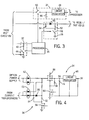
- FIG. 3 is a somewhat more detailed view of the power supplies and measurement circuitry of FIG. 3 coupled to the processor;
- FIG. 4 is a diagrammatical representation of a circuit configuration in which power from an add-on device or option module may be used when coupled to the device of the previous figures.
- power circuitry 10 is generally illustrated for supplying power to a motor 12.
- the power circuitry may be designed for stand-alone operation, or may be part of an overall control system, such as in industrial, commercial, material handling, or any other suitable applications (e.g., coupled to other components and networked to remote monitoring and control equipment).
- the circuitry includes an overload relay, designated generally by reference numeral 14, that senses voltage and current provided to the motor and that may open the power supply circuitry based upon actual or anticipated overload conditions.
- the overload relay 14 may be used with other protective circuitry, indicated generally by reference numeral 16.
- Such protective circuitry which may include fuses, manual or automatic disconnects, and so forth will typically be positioned between the overload relay and a power source, such as the power grid.
- Three-phase power in the illustrated embodiment, is provided to the protective circuitry, flows through the overload relay, and is then applied to motor drive circuitry 18 which powers the motor.
- the motor drive circuitry may include any suitable devices, such as across-the-line starters, soft starters, variable frequency motor drives, and so forth.
- the overload relay 14, in the illustrated example of FIG. 1 utilizes a series of current transformers 20 which are coupled to the three-phase power conductors passing through the device.
- Any type of current transformer may be used for the application, such as transformers comprising multiple winds of wire positioned about or next to the three-phase power conductors.
- the coils of the current transformers effectively act as secondary windings of transformers, and carry current induced by fields generated by current through the three-phase power conductors.
- the current transformers 20 apply the sensed signals to control circuitry 22, described in greater detail below.
- the control circuitry 22 takes measurements of current and voltage, and includes a processor that can cause tripping of the device based upon actual or anticipated overload conditions.
- control circuitry regulates power for measurement and for operation of the device by a power management scheme.
- the overload control circuitry 22 can open contacts 24 in the device to interrupt power to the motor.
- the control circuit can output signals to energize coils 38 that operate to open or close the contacts of the relay, in a manner well understood to those skilled in the art.
- the overload relay includes a processor 26 which serves to implement the power management scheme, and to analyze sensed data to determine when a condition exists that may warrant opening of the contacts 24.
- the processor is coupled to the current transformers via a rectification circuit 28. Because the waveform originating in the current transformers will reflect the sinusoidal waveform through the three-phase power conductors, rectification through circuit 28 serves to convert the three-phase AC power to DC power.
- a current measurement signal indicated by reference numeral 30 is applied to the processor 26 as output by the rectification circuit 28. Measurements necessary for the decisions implemented by the processor 26 are made by measurement circuit 32. The measurements made by the measurement circuit 32 are based upon current through a burden resistor in the circuit that is switched into and out of the circuitry as described more fully below.
- the processor 26 is coupled to an operational power supply 34, and to a trip/reset power supply 36.
- the operational power supply and the trip/reset power supply are both coupled to the rectified power provided by the rectification circuit 28.
- power storage components, such as capacitors, within the operational power supply and the trip/reset power supply are charged under the direction of control signals from the processor 26, in coordination with measurement by the measurement circuit 32.
- the operational power supply34 then, supplies power to the processor 26 during operation.
- the trip/reset power supply 36 stores and supplies power to open or close (i.e., reset) the contacts as commanded by the processor 26. This power supply, too, is charged under the direction of control signals provided by the processor 26.
- the processor 26 may also be coupled to various options, as indicated generally by reference numeral 40.
- options may include, for example, modules that may be coupled to, or plugged directly into the relay.
- Option modules presently contemplated may include inputs and outputs for communicating with the processor, remote reset devices, network interface devices, and so forth.
- Such option modules may then be coupled to external devices, such as remote control and monitoring equipment.
- such option modules may be separately powered, such as by a network link. As described more fully below, when this is the case, power from the network may be used to drive measurement and supply power for the power supply of the device.
- FIG. 3 illustrates the voltage/current measurement circuit 32 and power supplies 34 and 36 in somewhat greater detail in accordance with a presently contemplated implementation.
- the measurement circuit 32 includes a burden resistor 42 and a switch 44.
- Switch 44 may be any suitable switch, such as a transistor.
- the output of the rectification circuit 28 which serves as the input to the voltage measurement circuit 32 functionally resembles a current source with a somewhat variable voltage.
- the burden resistor 42 permits measurement of the line current by measuring a proportional current through the burden resistor to ground upon closing of switch 44. Opening and closing of switch 44 is controlled by processor 26 as described more fully below.
- the burden resistor Because current through the burden resistor is used to measure a voltage proportional to current, the burden resistor, if left in the circuit, represents a drain of power. By commanding switch 44 to open, the processor stops this drain and can use available power to charge components within the operational power supply 34 and the trip/reset power supply 36.
- the processor 26 also controls power supplies 34 and 36 by appropriately charging components within those power supplies via switches.
- power supply 34 includes a capacitor 46 which is charged to supply operational power for the device. Capacitor 46 is coupled to a linear regulator 48 which conditions and regulates the output power for operation of the processor.
- a switch 50 which again may be a transistor, is opened and closed by signals from processor 26.
- power supply 36 includes a pair of capacitors 52 and 54 separated by a diode 56. Charging of the capacitors is regulated by operation of a switch 58 on the controller processor 26.
- capacitors 46, 52 and 54 provide bulk storage for charge that can be drained for operation of the circuitry in the case of capacitor 46, and for tripping (opening the contacts) of the device and resetting the device in the case of capacitors 52 and 54.
- the reset capacitor may be used, for example, for automatic reset of the contacts.
- the processor 26 may be provided with electronically erasable programmable read-only memory, flash memory, or any other suitable memory circuitry. Programming for analyzing the current and voltage signals, and any other signals collected by the processor is stored within this memory. Moreover, for certain types of memory, reprogramming of the device may be performed by altering the programming stored within this memory, such as via an option module of the type described above with reference to FIG. 2 .
- the processor 26 closes switch 44 to make voltage measurements (proportional to current) at intervals when switches 50 and 58 are open. Once data has been collected for the measurement, then, switch 44 may be opened, and switches 50 and 58 may be closed to store power collected by the current transformers by charging capacitors 46, 52 and 54.
- the switches are alternatively opened and closed to perform measurements and store power, with a measurement period occurring every 1 ms.
- Other intervals and periods for alternative measurement and charging may, of course, be used, and durations for measurement and charging need not be equal.
- Certain functions may also be set by other means, such as resets, trip classes, and so forth may be set by appropriate dip switches (not shown). These functions may be implemented by virtue of the use of the processor to control operation of the device.
- FIG. 4 represents exemplary circuitry for this type of alternative power configuration.
- the power supplies 34 and 36 are essentially identical to those shown in FIG. 3 .
- a pair of diodes 60 prevents power from an option module from being transmitted back to the upstream circuitry.
- a pair of diodes 62 isolates the option power supply.
- Power supplies 34 and 36 may be powered by either the power supply or the current transformers, depending upon if the power supply that provides the higher voltage.
- FIG. 4 includes a solid state switch 64 that controls operation of switch 50.
- This configuration may be preferred such that switch 50 may be normally on (such as a JFET), allowing for cold start, that is, when no power is available to place the switch in a conductive state to charge the power supply.
- a resistor 66 is provided to hold the switch on ( i.e., pull the switch down).
- capacitors 46, 52 and 54 have values of 4.7 ⁇ F, 680 ⁇ F, and 680 ⁇ F, respectively, although differently sized capacitors may be employed depending upon the power needs and the power budget of the circuitry.
Landscapes
- Emergency Protection Circuit Devices (AREA)
Abstract
Description
- The present invention relates generally to protective circuitry, such as overload circuits. More particularly, the invention relates to a processor-based overload relay that is self-powered by virtue of power management components, permitting power to be stored for its operation, while performing measurements of voltage and current.
- Overload relays and similar circuits are used in a wide range of settings. For example, applications involving powering electric motors, a motor starter or motor controller is typically coupled to a motor to supply single or three-phase power. The motor drive, in many applications, may synthesize an output waveform to vary the frequency of the drive power so as to permit the motor to be driven at various speeds. The waveform may also be manipulated to control torque, and so forth. Motor controllers, however, do not typically provide for interrupting power to the motor in case of need. Depending upon the circuit configuration, other protective devices typically serve this purpose. Such devices may include fuses that are often positioned upstream of all other circuitry and downstream of a power supply, such as the electric power grid. The fuses may be supplemented by magnetic and thermal overload circuitry. Magnetic overload circuitry typically trips to open the power circuit in response to rapid changes in current. Other overload circuitry may operate more slowly, and may model motor windings or other wiring, to permit opening of the circuitry should longer-term rises in temperature be detected or estimated.
- In the area of overload relays, a number of different configurations have been developed and are presently in use. Such relays can be vary from quite simple electro-mechanical devices to more sophisticated circuitry that incorporates application specific integrated circuits (ASICs), or processors, typically microprocessors. Such ASICs and processors offer a significant benefit in being capable of analyzing current and voltage data and judiciously opening or closing power circuits based upon the analysis. Where possible, sophisticated yet high production (and thus cost effective) processors, including microprocessors and field programmable gate arrays may be used for such purposes.
- One challenge in the use of such circuitry, however, is the ability to provide sufficient power for its operation. Specifically, smaller sizes of overload relays may not be able to provide sufficient power for operation of microprocessor-based control circuitry. In many cases, it is advantageous to power the circuitry from power that is extracted or scavenged from the sensing devices, such as current transformers. However, where power levels required for the processing exceed the available power budget, more costly and less flexible ASICs and other circuitry may be required.
- There is a need, therefore, for improved circuit designs that may permit the use of more sophisticated processing capabilities that are powered by current transformers and similar power scavenging devices. There is a particular need for such circuitry that may permit microprocessors and similar circuits to be used in small electro-mechanical devices, such as overload relays, that have a reduced power budget.
- The present invention provides novel circuitry that can be used in overload relays and similar devices configured to respond to such needs. The circuitry may be used in a wide range of settings, but is particularly well-suited to devices where currents and/or voltages are measured and where circuit interruption is powered by power scavenged from the measurement circuits. In accordance with certain aspects of the invention, a processor implements a power management scheme in which a measurement circuit is periodically switched, along with power supply circuitry. The power supply circuitry may include power storage devices, such as capacitors, and more than one power supply circuit may be powered, such as one for operational power and one for tripping and resetting the circuitry. The measurement circuitry may include a burden resistor that is switched into an out of the power supply line from sensors in order to make periodic voltage measurements that are proportional to current. The power may also be provided, in the alternative, from add-on devices or networked option modules which are coupled to the processor, but for which the scavenging power supplies do not have sufficient power.
- These and other features, aspects, and advantages of the present invention will become better understood when the following detailed description is read with reference to the accompanying drawings in which like characters represent like parts throughout the drawings, wherein:
-
FIG. 1 is a diagrammatical representation of power supply circuitry in a motor application incorporating a relay in accordance with aspects of the present techniques; -
FIG. 2 is a diagrammatical representation of the circuitry ofFIG. 1 in greater detail, illustrating voltage/current measurement circuitry and power supplies commanded by a processor; -
FIG. 3 is a somewhat more detailed view of the power supplies and measurement circuitry ofFIG. 3 coupled to the processor; and -
FIG. 4 is a diagrammatical representation of a circuit configuration in which power from an add-on device or option module may be used when coupled to the device of the previous figures. - Turning now to the drawings, and referring first to
FIG. 1 ,power circuitry 10 is generally illustrated for supplying power to amotor 12. The power circuitry may be designed for stand-alone operation, or may be part of an overall control system, such as in industrial, commercial, material handling, or any other suitable applications (e.g., coupled to other components and networked to remote monitoring and control equipment). The circuitry includes an overload relay, designated generally byreference numeral 14, that senses voltage and current provided to the motor and that may open the power supply circuitry based upon actual or anticipated overload conditions. Theoverload relay 14 may be used with other protective circuitry, indicated generally byreference numeral 16. Such protective circuitry, which may include fuses, manual or automatic disconnects, and so forth will typically be positioned between the overload relay and a power source, such as the power grid. Three-phase power, in the illustrated embodiment, is provided to the protective circuitry, flows through the overload relay, and is then applied tomotor drive circuitry 18 which powers the motor. The motor drive circuitry may include any suitable devices, such as across-the-line starters, soft starters, variable frequency motor drives, and so forth. - The
overload relay 14, in the illustrated example ofFIG. 1 , utilizes a series ofcurrent transformers 20 which are coupled to the three-phase power conductors passing through the device. Any type of current transformer may be used for the application, such as transformers comprising multiple winds of wire positioned about or next to the three-phase power conductors. The coils of the current transformers effectively act as secondary windings of transformers, and carry current induced by fields generated by current through the three-phase power conductors. Thecurrent transformers 20 apply the sensed signals to controlcircuitry 22, described in greater detail below. Thecontrol circuitry 22 takes measurements of current and voltage, and includes a processor that can cause tripping of the device based upon actual or anticipated overload conditions. As also described below, the control circuitry regulates power for measurement and for operation of the device by a power management scheme. In the event of an overload condition, theoverload control circuitry 22 can opencontacts 24 in the device to interrupt power to the motor. Finally, the control circuit can output signals to energizecoils 38 that operate to open or close the contacts of the relay, in a manner well understood to those skilled in the art. - As best illustrated in
FIG. 2 , the overload relay includes aprocessor 26 which serves to implement the power management scheme, and to analyze sensed data to determine when a condition exists that may warrant opening of thecontacts 24. The processor is coupled to the current transformers via arectification circuit 28. Because the waveform originating in the current transformers will reflect the sinusoidal waveform through the three-phase power conductors, rectification throughcircuit 28 serves to convert the three-phase AC power to DC power. A current measurement signal indicated byreference numeral 30 is applied to theprocessor 26 as output by therectification circuit 28. Measurements necessary for the decisions implemented by theprocessor 26 are made bymeasurement circuit 32. The measurements made by themeasurement circuit 32 are based upon current through a burden resistor in the circuit that is switched into and out of the circuitry as described more fully below. - As also illustrated in
FIG. 2 , theprocessor 26 is coupled to anoperational power supply 34, and to a trip/reset power supply 36. The operational power supply and the trip/reset power supply are both coupled to the rectified power provided by therectification circuit 28. In operation, power storage components, such as capacitors, within the operational power supply and the trip/reset power supply are charged under the direction of control signals from theprocessor 26, in coordination with measurement by themeasurement circuit 32. The operational power supply34, then, supplies power to theprocessor 26 during operation. The trip/reset power supply 36 stores and supplies power to open or close (i.e., reset) the contacts as commanded by theprocessor 26. This power supply, too, is charged under the direction of control signals provided by theprocessor 26. - In the illustrated embodiment, the
processor 26 may also be coupled to various options, as indicated generally byreference numeral 40. Such options may include, for example, modules that may be coupled to, or plugged directly into the relay. Option modules presently contemplated may include inputs and outputs for communicating with the processor, remote reset devices, network interface devices, and so forth. Such option modules may then be coupled to external devices, such as remote control and monitoring equipment. In many applications such option modules may be separately powered, such as by a network link. As described more fully below, when this is the case, power from the network may be used to drive measurement and supply power for the power supply of the device. -
FIG. 3 illustrates the voltage/current measurement circuit 32 andpower supplies FIG. 3 , themeasurement circuit 32 includes aburden resistor 42 and aswitch 44.Switch 44 may be any suitable switch, such as a transistor. As will be appreciated by those skilled in the art, the output of therectification circuit 28 which serves as the input to thevoltage measurement circuit 32 functionally resembles a current source with a somewhat variable voltage. Theburden resistor 42 permits measurement of the line current by measuring a proportional current through the burden resistor to ground upon closing ofswitch 44. Opening and closing ofswitch 44 is controlled byprocessor 26 as described more fully below. Because current through the burden resistor is used to measure a voltage proportional to current, the burden resistor, if left in the circuit, represents a drain of power. By commandingswitch 44 to open, the processor stops this drain and can use available power to charge components within theoperational power supply 34 and the trip/resetpower supply 36. - The
processor 26 also controlspower supplies FIG. 3 , for example,power supply 34 includes acapacitor 46 which is charged to supply operational power for the device.Capacitor 46 is coupled to alinear regulator 48 which conditions and regulates the output power for operation of the processor. Aswitch 50, which again may be a transistor, is opened and closed by signals fromprocessor 26. Similarly,power supply 36 includes a pair ofcapacitors diode 56. Charging of the capacitors is regulated by operation of aswitch 58 on thecontroller processor 26. In the present embodiment,capacitors capacitor 46, and for tripping (opening the contacts) of the device and resetting the device in the case ofcapacitors - The
processor 26 may be provided with electronically erasable programmable read-only memory, flash memory, or any other suitable memory circuitry. Programming for analyzing the current and voltage signals, and any other signals collected by the processor is stored within this memory. Moreover, for certain types of memory, reprogramming of the device may be performed by altering the programming stored within this memory, such as via an option module of the type described above with reference toFIG. 2 . In operation, theprocessor 26 closes switch 44 to make voltage measurements (proportional to current) at intervals when switches 50 and 58 are open. Once data has been collected for the measurement, then, switch 44 may be opened, and switches 50 and 58 may be closed to store power collected by the current transformers by chargingcapacitors - In certain applications where option modules are coupled to the circuitry described above and separately powered, such as through a network, this option module power may be used instead of scavenged power from the current transformers.
FIG. 4 represents exemplary circuitry for this type of alternative power configuration. As shown inFIG. 4 , the power supplies 34 and 36 are essentially identical to those shown inFIG. 3 . However, a pair ofdiodes 60 prevents power from an option module from being transmitted back to the upstream circuitry. Similarly, a pair ofdiodes 62 isolates the option power supply. Power supplies 34 and 36 may be powered by either the power supply or the current transformers, depending upon if the power supply that provides the higher voltage. - As compared to the circuitry shown in
FIG. 3 , that ofFIG. 4 includes asolid state switch 64 that controls operation ofswitch 50. This configuration may be preferred such thatswitch 50 may be normally on (such as a JFET), allowing for cold start, that is, when no power is available to place the switch in a conductive state to charge the power supply. Aresistor 66 is provided to hold the switch on (i.e., pull the switch down). In a presently contemplated embodiment,capacitors - While only certain features of the invention have been illustrated and described herein, many modifications and changes will occur to those skilled in the art. It is, therefore, to be understood that the appended claims are intended to cover all such modifications and changes as fall within the true spirit of the invention.
-
- Embodiment 1: An electro-mechanical device comprising:
- a current transformer configured to provide power based upon current through a conductor;
- a measurement circuit coupled to the current transformer and configured to measure a current and/or voltage from the transformer;
- a power supply circuit coupled to the current transformer and configured to store charge when receiving the power; and
- a processor coupled to the measurement circuit and to the power supply circuit and configured to alternatively enable measurements by the measurement circuit and to charge a storage device in the power supply circuit.
- Embodiment 2: The device of embodiment 1, comprising three current transformers configured to provide power in response to current through three phase conductors.
- Embodiment 3: The device of embodiment 1, comprising rectification circuitry configured to rectify a waveform output by the current transformer to provide rectified power to the measurement circuit, the power supply circuit and the processor.
- Embodiment 4: The device of embodiment 1, wherein the measurement circuit includes a burden resistor and a solid state switch, the solid state switch being coupled to the processor to selectively place the burden resistor in series between an output of the current transformer and a reference potential to permit a measurement.
- Embodiment 5: The device of embodiment 1, wherein the power supply includes a capacitor and a solid state switch, the solid state switch being coupled to the processor to selectively place the capacitor in series between an output of the current transformer and a reference potential to charge the capacitor.
- Embodiment 6: The device of embodiment 1, comprising two power supply circuits coupled to the current transformer and to the processor, the power supply circuits being switched to a charging state by the processor when the measurement circuit is not performing measurements.
- Embodiment 7: The device of embodiment 6, wherein the power supply circuits include an operational power supply circuit for providing power for the processor, and a trip power supply circuit for opening contacts in the device.
- Embodiment 8: The device of embodiment 1, comprising an alternative power supply circuit in parallel with the power from the current transformer for providing power for charging the power supply.
- Embodiment 9: The device of embodiment 1, wherein the alternative power supply circuit is coupled to an add-on device.
- Embodiment 10: An electro-mechanical device comprising:
- a set of current transformers configured to provide power based upon current through three phase conductors;
- a rectification circuit coupled to the current transformers for converting power from the current transformers to rectified power;
- a measurement circuit coupled to the rectification circuit for measuring a signal indicative of current and/or voltage from the rectification circuit, the measurement circuit including a first solid state switch;
- a power supply circuit coupled to the rectification circuit and configured to store charge when receiving the rectified power, the power supply circuit including a second solid state switch; and
- a processor coupled to the measurement circuit and to the power supply circuit and configured to switch the solid state switches to enable measurements by the measurement circuit and alternatively to charge a storage device in the power supply circuit.
- Embodiment 11: The device of
embodiment 10, wherein the measurement circuit includes a burden resistor in series with the first solid state switch, the first solid state switch being coupled to the processor to selectively place the burden resistor in series between an output of the rectification circuit and a reference potential to permit measurement of the signal. - Embodiment 12: The device of embodiment 11, wherein the power supply includes a capacitor in series with the second solid state switch, the second solid state switch being coupled to the processor to selectively place the capacitor in series between an output of the rectification circuit and a reference potential to charge the capacitor.
- Embodiment 13: The device of
embodiment 12, comprising two power supply circuits coupled to the rectification circuit and to the processor, the power supply circuits being switched to a charging state by the processor when the measurement circuit is not performing measurements. - Embodiment 14: The device of embodiment 13, wherein the power supply circuits include an operational power supply circuit for providing power for the processor, and a trip power supply circuit for opening contacts in the device.
- Embodiment 15: The device of
embodiment 10, comprising an alternative power supply circuit in parallel with the power from the current transformer for providing power for charging the power supply. - Embodiment 16: A method for operating an electro-mechanical device, comprising:
- (a) applying a first signal from a processor to a first solid state switch of a measurement circuit to place a burden resistor in series between a supply of rectified power and a reference potential to measure a signal representative of voltage and/or current;
- (b) removing the first signal to interrupt current through the burden resistor and applying a second signal from the processor to a second solid state switch of a power supply circuit to place a storage capacitor in series between the supply of rectified power and a reference potential to charge the capacitor, the processor being powered by discharge of the capacitor.
- Embodiment 17: The method of
embodiment 16, comprising:- (c) removing the second signal to interrupt current to the capacitor, and reapplying the first signal as in step (a).
- Embodiment 18: The method of embodiment 17, comprising cyclically repeating steps (b) and (c).
- Embodiment 19: The method of
embodiment 16, wherein step (b) comprises applying a third signal from the processor to a third solid state switch of a further power supply circuit to place a further storage capacitor in series between the supply of rectified power and a reference potential to charge the further capacitor, the second power supply being coupled to trip circuitry for opening contacts in the device. - Embodiment 20: The method of embodiment 19, wherein the second and third signals are applied to the second and third switches simultaneously.
Claims (15)
- An electro-mechanical device comprising:a current transformer configured to provide power based upon current through a conductor;a measurement circuit coupled to the current transformer and configured to measure a current and/or voltage from the transformer;a power supply circuit coupled to the current transformer and configured to store charge when receiving the power; anda processor coupled to the measurement circuit and to the power supply circuit and configured to alternatively enable measurements by the measurement circuit and to charge a storage device in the power supply circuit.
- The device of claim 1, comprising three current transformers configured to provide power in response to current through three phase conductors.
- The device of claim 1, comprising rectification circuitry configured to rectify a waveform output by the current transformer to provide rectified power to the measurement circuit, the power supply circuit and the processor.
- The device of claim 1, wherein the measurement circuit includes a burden resistor and a solid state switch, the solid state switch being coupled to the processor to selectively place the burden resistor in series between an output of the current transformer and a reference potential to permit a measurement.
- The device of claim 1, wherein the power supply includes a capacitor and a solid state switch, the solid state switch being coupled to the processor to selectively place the capacitor in series between an output of the current transformer and a reference potential to charge the capacitor.
- The device of claim 1, comprising two power supply circuits coupled to the current transformer and to the processor, the power supply circuits being switched to a charging state by the processor when the measurement circuit is not performing measurements, and wherein the power supply circuits include an operational power supply circuit for providing power for the processor, and a trip power supply circuit for opening contacts in the device.
- The device of claim 1, comprising an alternative power supply circuit in parallel with the power from the current transformer for providing power for charging the power supply, wherein the alternative power supply circuit is coupled to an add-on device.
- An electro-mechanical device comprising:a set of current transformers configured to provide power based upon current through three phase conductors;a rectification circuit coupled to the current transformers for converting power from the current transformers to rectified power;a measurement circuit coupled to the rectification circuit for measuring a signal indicative of current and/or voltage from the rectification circuit, the measurement circuit including a first solid state switch;a power supply circuit coupled to the rectification circuit and configured to store charge when receiving the rectified power, the power supply circuit including a second solid state switch; anda processor coupled to the measurement circuit and to the power supply circuit and configured to switch the solid state switches to enable measurements by the measurement circuit and alternatively to charge a storage device in the power supply circuit.
- The device of claim 8, wherein the measurement circuit includes a burden resistor in series with the first solid state switch, the first solid state switch being coupled to the processor to selectively place the burden resistor in series between an output of the rectification circuit and a reference potential to permit measurement of the signal, and wherein the power supply includes a capacitor in series with the second solid state switch, the second solid state switch being coupled to the processor to selectively place the capacitor in series between an output of the rectification circuit and a reference potential to charge the capacitor.
- The device of claim 9, comprising two power supply circuits coupled to the rectification circuit and to the processor, the power supply circuits being switched to a charging state by the processor when the measurement circuit is not performing measurements, and wherein the power supply circuits include an operational power supply circuit for providing power for the processor, and a trip power supply circuit for opening contacts in the device.
- The device of claim 8, comprising an alternative power supply circuit in parallel with the power from the current transformer for providing power for charging the power supply.
- A method for operating an electro-mechanical device, comprising:(a) applying a first signal from a processor to a first solid state switch of a measurement circuit to place a burden resistor in series between a supply of rectified power and a reference potential to measure a signal representative of voltage and/or current;(b) removing the first signal to interrupt current through the burden resistor and applying a second signal from the processor to a second solid state switch of a power supply circuit to place a storage capacitor in series between the supply of rectified power and a reference potential to charge the capacitor, the processor being powered by discharge of the capacitor.
- The method of claim 12, comprising:(c) removing the second signal to interrupt current to the capacitor, and reapplying the first signal as in step (a).
- The method of claim 13, comprising cyclically repeating steps (b) and (c).
- The method of claim 12, wherein step (b) comprises applying a third signal from the processor to a third solid state switch of a further power supply circuit to place a further storage capacitor in series between the supply of rectified power and a reference potential to charge the further capacitor, the second power supply being coupled to trip circuitry for opening contacts in the device, and wherein the second and third signals are applied to the second and third switches simultaneously.
Applications Claiming Priority (1)
| Application Number | Priority Date | Filing Date | Title |
|---|---|---|---|
| US12/242,479 US7907375B2 (en) | 2008-09-30 | 2008-09-30 | Self powered electronic overload method and system |
Publications (3)
| Publication Number | Publication Date |
|---|---|
| EP2169798A2 true EP2169798A2 (en) | 2010-03-31 |
| EP2169798A3 EP2169798A3 (en) | 2013-06-19 |
| EP2169798B1 EP2169798B1 (en) | 2016-03-23 |
Family
ID=41416205
Family Applications (1)
| Application Number | Title | Priority Date | Filing Date |
|---|---|---|---|
| EP09171779.3A Not-in-force EP2169798B1 (en) | 2008-09-30 | 2009-09-30 | Self Powered Electronic Overload Method and System |
Country Status (2)
| Country | Link |
|---|---|
| US (1) | US7907375B2 (en) |
| EP (1) | EP2169798B1 (en) |
Cited By (6)
| Publication number | Priority date | Publication date | Assignee | Title |
|---|---|---|---|---|
| WO2012096863A1 (en) * | 2011-01-12 | 2012-07-19 | Schneider Electric USA, Inc. | System and method for monitoring current drawn by a protected load in a self-powered electronic protection device |
| WO2012104270A1 (en) * | 2011-01-31 | 2012-08-09 | Eliwell Controls S.R.L. Con Unico Socio | Device and method for measuring an alternating voltage |
| GB2489517A (en) * | 2011-03-31 | 2012-10-03 | Seamless Sensing Ltd | Current sensor with switching device for energy storage and method for controlling appliances connected to a grid |
| CN104749412A (en) * | 2013-12-30 | 2015-07-01 | 西门子公司 | Sampling system of electric leakage protection device |
| WO2016078874A1 (en) * | 2014-11-18 | 2016-05-26 | Eaton Industries (Austria) Gmbh | Residual-current circuit breaker |
| CN107064597A (en) * | 2016-02-04 | 2017-08-18 | 阿尔卑斯电气株式会社 | The current sensor of self-powered |
Families Citing this family (11)
| Publication number | Priority date | Publication date | Assignee | Title |
|---|---|---|---|---|
| BRPI0520690A2 (en) * | 2005-11-21 | 2009-05-19 | Siemens Ag | manufacturing process of a starter for a three-phase electric motor and its starter |
| US9030793B2 (en) | 2012-04-13 | 2015-05-12 | General Electric Company | Method, device, and system for monitoring current provided to a load |
| US9664709B2 (en) | 2012-06-08 | 2017-05-30 | Neilsen-Kuljian, Inc. | Electrical sensor with configurable settings |
| US9747776B2 (en) | 2012-06-08 | 2017-08-29 | Neilsen-Kuljian, Inc. | Electrical sensor with configurable settings and a display |
| US9766273B2 (en) | 2012-08-21 | 2017-09-19 | Neilsen-Kuljian, Inc. | Self-powered current sensor with a linear adjustment |
| US9559513B2 (en) * | 2012-11-02 | 2017-01-31 | Rockwell Automation Technologies, Inc. | Voltage sensor contact for an electronic device |
| CN108418214A (en) * | 2018-03-28 | 2018-08-17 | 国网江苏省电力有限公司南京供电分公司 | A kind of power grid adjusting method based on convertible frequency air-conditioner load |
| CN109412123B (en) * | 2018-11-26 | 2024-04-30 | 烟台市华能电器有限公司 | 10KV power line CT power supply control system passive storage/query circuit |
| EP4005056A4 (en) * | 2019-07-30 | 2023-04-12 | Cummins Inc. | TECHNOLOGY FOR GENERATION OF BACKUP POWER FOR CLOCKS AND CRITICAL DATA BACKUPS FOR CONTROL DEVICES |
| EP4016574B1 (en) * | 2020-12-15 | 2023-06-28 | ABB Schweiz AG | A hybrid switching apparatus for electric grids |
| CN220043039U (en) | 2023-03-29 | 2023-11-17 | 施耐德电气工业公司 | Power supply circuit and electrical device |
Family Cites Families (4)
| Publication number | Priority date | Publication date | Assignee | Title |
|---|---|---|---|---|
| US4271447A (en) * | 1979-07-31 | 1981-06-02 | General Electric Company | Power supply for circuit breaker static trip unit |
| DE3331823A1 (en) * | 1983-09-01 | 1985-03-21 | Siemens AG, 1000 Berlin und 8000 München | POWER SUPPLY DEVICE FOR AN OVERCURRENT RELEASE |
| US6018700A (en) * | 1998-02-19 | 2000-01-25 | Edel; Thomas G. | Self-powered current monitor |
| US7788055B2 (en) * | 2006-07-14 | 2010-08-31 | Square D Company | Method and system of calibrating sensing components in a circuit breaker system |
-
2008
- 2008-09-30 US US12/242,479 patent/US7907375B2/en active Active
-
2009
- 2009-09-30 EP EP09171779.3A patent/EP2169798B1/en not_active Not-in-force
Cited By (11)
| Publication number | Priority date | Publication date | Assignee | Title |
|---|---|---|---|---|
| WO2012096863A1 (en) * | 2011-01-12 | 2012-07-19 | Schneider Electric USA, Inc. | System and method for monitoring current drawn by a protected load in a self-powered electronic protection device |
| US8854032B2 (en) | 2011-01-12 | 2014-10-07 | Schneider Electric USA, Inc. | System and method for monitoring current drawn by a protected load in a self-powered electronic protection device |
| WO2012104270A1 (en) * | 2011-01-31 | 2012-08-09 | Eliwell Controls S.R.L. Con Unico Socio | Device and method for measuring an alternating voltage |
| CN103443636A (en) * | 2011-01-31 | 2013-12-11 | 伊利威尔康特罗斯单一股份有限公司 | Device and method for measuring AC voltage |
| CN103443636B (en) * | 2011-01-31 | 2016-06-29 | 伊利威尔康特罗斯单一股份有限公司 | Device and method for measuring AC voltage |
| GB2489517A (en) * | 2011-03-31 | 2012-10-03 | Seamless Sensing Ltd | Current sensor with switching device for energy storage and method for controlling appliances connected to a grid |
| CN104749412A (en) * | 2013-12-30 | 2015-07-01 | 西门子公司 | Sampling system of electric leakage protection device |
| CN104749412B (en) * | 2013-12-30 | 2018-04-10 | 西门子公司 | The sampling system of earth leakage protective device |
| WO2016078874A1 (en) * | 2014-11-18 | 2016-05-26 | Eaton Industries (Austria) Gmbh | Residual-current circuit breaker |
| CN107064597A (en) * | 2016-02-04 | 2017-08-18 | 阿尔卑斯电气株式会社 | The current sensor of self-powered |
| CN107064597B (en) * | 2016-02-04 | 2021-03-12 | 阿尔卑斯阿尔派株式会社 | Self-powered current sensor |
Also Published As
| Publication number | Publication date |
|---|---|
| US20100079922A1 (en) | 2010-04-01 |
| EP2169798B1 (en) | 2016-03-23 |
| EP2169798A3 (en) | 2013-06-19 |
| US7907375B2 (en) | 2011-03-15 |
Similar Documents
| Publication | Publication Date | Title |
|---|---|---|
| US7907375B2 (en) | Self powered electronic overload method and system | |
| CN113474948B (en) | Device for protecting and controlling an electrical load | |
| US11391778B2 (en) | Category specific industrial battery optimization and restoration device, with battery diagnostics, battery life prognostication, and an artificial intelligence means | |
| CN1819412B (en) | Insulation resistance deterioration detection method and insulation resistance deterioration detection device for motor, and motor driver | |
| US9000611B2 (en) | Protection techniques for an electric power system | |
| CN106415968B (en) | Semi-voltage dependent circuit breaker | |
| US5220495A (en) | Arrangement and method for accurately sensing voltage of a high-impedance source and supplying power to a variable burden | |
| US5754386A (en) | Trip device for an electric powered trip unit | |
| EP3414812B1 (en) | Apparatus, system and method for power extraction | |
| CA2319409A1 (en) | Self-powered current monitor | |
| CN107438890B (en) | Electronic trip unit powered by a current transformer and circuit breaker comprising same | |
| EP3929599B1 (en) | Multi-phase vfd system with frequency compensated ground fault protection | |
| CN1270340C (en) | Electronic tripping device including capacitor as trippin coil power source | |
| EP3084800B1 (en) | Electrical switching apparatus including alternating current electronic trip circuit with arc fault detection circuit and power supply | |
| US7646275B2 (en) | Device and method for eliminating transformer excitation losses | |
| US6101105A (en) | Apparatus and method for identifying an unregulated DC bus voltage | |
| US6252752B1 (en) | Overload protection apparatus and a speed reducer having such an apparatus | |
| US11804789B2 (en) | System and method for protecting an electrical load of a drive system | |
| Sedhuraman et al. | Performance evaluation of smart intelligent circuit breaker | |
| CN211206716U (en) | Detection device of switch equipment | |
| CN208299438U (en) | power supply device | |
| RU2279686C1 (en) | Arrangement for definition of the group of joining of the windings of a three-phase transformer | |
| EP0135870A1 (en) | Process and device for the overload protection of electrical energy consumers | |
| Egwaile et al. | Design and Construction of a Programmable Password Operated Circuit Breaker | |
| CN2572546Y (en) | Intelligent low voltage switch equipment |
Legal Events
| Date | Code | Title | Description |
|---|---|---|---|
| PUAI | Public reference made under article 153(3) epc to a published international application that has entered the european phase |
Free format text: ORIGINAL CODE: 0009012 |
|
| AK | Designated contracting states |
Kind code of ref document: A2 Designated state(s): AT BE BG CH CY CZ DE DK EE ES FI FR GB GR HR HU IE IS IT LI LT LU LV MC MK MT NL NO PL PT RO SE SI SK SM TR |
|
| AX | Request for extension of the european patent |
Extension state: AL BA RS |
|
| PUAL | Search report despatched |
Free format text: ORIGINAL CODE: 0009013 |
|
| RIC1 | Information provided on ipc code assigned before grant |
Ipc: H02H 3/05 20060101ALN20130502BHEP Ipc: H02H 7/08 20060101ALN20130502BHEP Ipc: H02H 1/06 20060101AFI20130502BHEP Ipc: H02H 7/085 20060101ALI20130502BHEP Ipc: H02J 9/00 20060101ALI20130502BHEP |
|
| AK | Designated contracting states |
Kind code of ref document: A3 Designated state(s): AT BE BG CH CY CZ DE DK EE ES FI FR GB GR HR HU IE IS IT LI LT LU LV MC MK MT NL NO PL PT RO SE SI SK SM TR |
|
| AX | Request for extension of the european patent |
Extension state: AL BA RS |
|
| 17P | Request for examination filed |
Effective date: 20131206 |
|
| RBV | Designated contracting states (corrected) |
Designated state(s): AT BE BG CH CY CZ DE DK EE ES FI FR GB GR HR HU IE IS IT LI LT LU LV MC MK MT NL NO PL PT RO SE SI SK SM TR |
|
| GRAP | Despatch of communication of intention to grant a patent |
Free format text: ORIGINAL CODE: EPIDOSNIGR1 |
|
| RIC1 | Information provided on ipc code assigned before grant |
Ipc: H02J 9/00 20060101ALI20150611BHEP Ipc: H02H 1/06 20060101AFI20150611BHEP Ipc: H02H 7/08 20060101ALN20150611BHEP Ipc: H02H 3/05 20060101ALN20150611BHEP Ipc: H02H 7/085 20060101ALI20150611BHEP |
|
| INTG | Intention to grant announced |
Effective date: 20150706 |
|
| GRAP | Despatch of communication of intention to grant a patent |
Free format text: ORIGINAL CODE: EPIDOSNIGR1 |
|
| INTG | Intention to grant announced |
Effective date: 20151126 |
|
| RIC1 | Information provided on ipc code assigned before grant |
Ipc: H02H 7/085 20060101ALI20151117BHEP Ipc: H02J 9/00 20060101ALI20151117BHEP Ipc: H02H 1/06 20060101AFI20151117BHEP Ipc: H02H 7/08 20060101ALN20151117BHEP Ipc: H02H 3/05 20060101ALN20151117BHEP |
|
| GRAS | Grant fee paid |
Free format text: ORIGINAL CODE: EPIDOSNIGR3 |
|
| GRAA | (expected) grant |
Free format text: ORIGINAL CODE: 0009210 |
|
| AK | Designated contracting states |
Kind code of ref document: B1 Designated state(s): AT BE BG CH CY CZ DE DK EE ES FI FR GB GR HR HU IE IS IT LI LT LU LV MC MK MT NL NO PL PT RO SE SI SK SM TR |
|
| REG | Reference to a national code |
Ref country code: GB Ref legal event code: FG4D |
|
| REG | Reference to a national code |
Ref country code: CH Ref legal event code: EP |
|
| REG | Reference to a national code |
Ref country code: AT Ref legal event code: REF Ref document number: 783995 Country of ref document: AT Kind code of ref document: T Effective date: 20160415 |
|
| REG | Reference to a national code |
Ref country code: IE Ref legal event code: FG4D |
|
| REG | Reference to a national code |
Ref country code: DE Ref legal event code: R096 Ref document number: 602009036964 Country of ref document: DE |
|
| REG | Reference to a national code |
Ref country code: LT Ref legal event code: MG4D |
|
| REG | Reference to a national code |
Ref country code: NL Ref legal event code: MP Effective date: 20160323 |
|
| PG25 | Lapsed in a contracting state [announced via postgrant information from national office to epo] |
Ref country code: GR Free format text: LAPSE BECAUSE OF FAILURE TO SUBMIT A TRANSLATION OF THE DESCRIPTION OR TO PAY THE FEE WITHIN THE PRESCRIBED TIME-LIMIT Effective date: 20160624 Ref country code: NO Free format text: LAPSE BECAUSE OF FAILURE TO SUBMIT A TRANSLATION OF THE DESCRIPTION OR TO PAY THE FEE WITHIN THE PRESCRIBED TIME-LIMIT Effective date: 20160623 Ref country code: FI Free format text: LAPSE BECAUSE OF FAILURE TO SUBMIT A TRANSLATION OF THE DESCRIPTION OR TO PAY THE FEE WITHIN THE PRESCRIBED TIME-LIMIT Effective date: 20160323 |
|
| REG | Reference to a national code |
Ref country code: AT Ref legal event code: MK05 Ref document number: 783995 Country of ref document: AT Kind code of ref document: T Effective date: 20160323 |
|
| PG25 | Lapsed in a contracting state [announced via postgrant information from national office to epo] |
Ref country code: NL Free format text: LAPSE BECAUSE OF FAILURE TO SUBMIT A TRANSLATION OF THE DESCRIPTION OR TO PAY THE FEE WITHIN THE PRESCRIBED TIME-LIMIT Effective date: 20160323 Ref country code: LT Free format text: LAPSE BECAUSE OF FAILURE TO SUBMIT A TRANSLATION OF THE DESCRIPTION OR TO PAY THE FEE WITHIN THE PRESCRIBED TIME-LIMIT Effective date: 20160323 Ref country code: LV Free format text: LAPSE BECAUSE OF FAILURE TO SUBMIT A TRANSLATION OF THE DESCRIPTION OR TO PAY THE FEE WITHIN THE PRESCRIBED TIME-LIMIT Effective date: 20160323 Ref country code: SE Free format text: LAPSE BECAUSE OF FAILURE TO SUBMIT A TRANSLATION OF THE DESCRIPTION OR TO PAY THE FEE WITHIN THE PRESCRIBED TIME-LIMIT Effective date: 20160323 |
|
| REG | Reference to a national code |
Ref country code: FR Ref legal event code: PLFP Year of fee payment: 8 |
|
| PG25 | Lapsed in a contracting state [announced via postgrant information from national office to epo] |
Ref country code: PL Free format text: LAPSE BECAUSE OF FAILURE TO SUBMIT A TRANSLATION OF THE DESCRIPTION OR TO PAY THE FEE WITHIN THE PRESCRIBED TIME-LIMIT Effective date: 20160323 Ref country code: EE Free format text: LAPSE BECAUSE OF FAILURE TO SUBMIT A TRANSLATION OF THE DESCRIPTION OR TO PAY THE FEE WITHIN THE PRESCRIBED TIME-LIMIT Effective date: 20160323 Ref country code: IS Free format text: LAPSE BECAUSE OF FAILURE TO SUBMIT A TRANSLATION OF THE DESCRIPTION OR TO PAY THE FEE WITHIN THE PRESCRIBED TIME-LIMIT Effective date: 20160723 |
|
| PG25 | Lapsed in a contracting state [announced via postgrant information from national office to epo] |
Ref country code: SK Free format text: LAPSE BECAUSE OF FAILURE TO SUBMIT A TRANSLATION OF THE DESCRIPTION OR TO PAY THE FEE WITHIN THE PRESCRIBED TIME-LIMIT Effective date: 20160323 Ref country code: AT Free format text: LAPSE BECAUSE OF FAILURE TO SUBMIT A TRANSLATION OF THE DESCRIPTION OR TO PAY THE FEE WITHIN THE PRESCRIBED TIME-LIMIT Effective date: 20160323 Ref country code: CZ Free format text: LAPSE BECAUSE OF FAILURE TO SUBMIT A TRANSLATION OF THE DESCRIPTION OR TO PAY THE FEE WITHIN THE PRESCRIBED TIME-LIMIT Effective date: 20160323 Ref country code: SM Free format text: LAPSE BECAUSE OF FAILURE TO SUBMIT A TRANSLATION OF THE DESCRIPTION OR TO PAY THE FEE WITHIN THE PRESCRIBED TIME-LIMIT Effective date: 20160323 Ref country code: RO Free format text: LAPSE BECAUSE OF FAILURE TO SUBMIT A TRANSLATION OF THE DESCRIPTION OR TO PAY THE FEE WITHIN THE PRESCRIBED TIME-LIMIT Effective date: 20160323 Ref country code: ES Free format text: LAPSE BECAUSE OF FAILURE TO SUBMIT A TRANSLATION OF THE DESCRIPTION OR TO PAY THE FEE WITHIN THE PRESCRIBED TIME-LIMIT Effective date: 20160323 Ref country code: PT Free format text: LAPSE BECAUSE OF FAILURE TO SUBMIT A TRANSLATION OF THE DESCRIPTION OR TO PAY THE FEE WITHIN THE PRESCRIBED TIME-LIMIT Effective date: 20160725 |
|
| PG25 | Lapsed in a contracting state [announced via postgrant information from national office to epo] |
Ref country code: BE Free format text: LAPSE BECAUSE OF FAILURE TO SUBMIT A TRANSLATION OF THE DESCRIPTION OR TO PAY THE FEE WITHIN THE PRESCRIBED TIME-LIMIT Effective date: 20160323 Ref country code: IT Free format text: LAPSE BECAUSE OF FAILURE TO SUBMIT A TRANSLATION OF THE DESCRIPTION OR TO PAY THE FEE WITHIN THE PRESCRIBED TIME-LIMIT Effective date: 20160323 |
|
| REG | Reference to a national code |
Ref country code: DE Ref legal event code: R097 Ref document number: 602009036964 Country of ref document: DE |
|
| PLBE | No opposition filed within time limit |
Free format text: ORIGINAL CODE: 0009261 |
|
| STAA | Information on the status of an ep patent application or granted ep patent |
Free format text: STATUS: NO OPPOSITION FILED WITHIN TIME LIMIT |
|
| PG25 | Lapsed in a contracting state [announced via postgrant information from national office to epo] |
Ref country code: DK Free format text: LAPSE BECAUSE OF FAILURE TO SUBMIT A TRANSLATION OF THE DESCRIPTION OR TO PAY THE FEE WITHIN THE PRESCRIBED TIME-LIMIT Effective date: 20160323 |
|
| PG25 | Lapsed in a contracting state [announced via postgrant information from national office to epo] |
Ref country code: BG Free format text: LAPSE BECAUSE OF FAILURE TO SUBMIT A TRANSLATION OF THE DESCRIPTION OR TO PAY THE FEE WITHIN THE PRESCRIBED TIME-LIMIT Effective date: 20160623 |
|
| 26N | No opposition filed |
Effective date: 20170102 |
|
| PG25 | Lapsed in a contracting state [announced via postgrant information from national office to epo] |
Ref country code: MC Free format text: LAPSE BECAUSE OF FAILURE TO SUBMIT A TRANSLATION OF THE DESCRIPTION OR TO PAY THE FEE WITHIN THE PRESCRIBED TIME-LIMIT Effective date: 20160323 |
|
| REG | Reference to a national code |
Ref country code: CH Ref legal event code: PL |
|
| PG25 | Lapsed in a contracting state [announced via postgrant information from national office to epo] |
Ref country code: SI Free format text: LAPSE BECAUSE OF FAILURE TO SUBMIT A TRANSLATION OF THE DESCRIPTION OR TO PAY THE FEE WITHIN THE PRESCRIBED TIME-LIMIT Effective date: 20160323 |
|
| REG | Reference to a national code |
Ref country code: IE Ref legal event code: MM4A |
|
| PG25 | Lapsed in a contracting state [announced via postgrant information from national office to epo] |
Ref country code: LI Free format text: LAPSE BECAUSE OF NON-PAYMENT OF DUE FEES Effective date: 20160930 Ref country code: CH Free format text: LAPSE BECAUSE OF NON-PAYMENT OF DUE FEES Effective date: 20160930 Ref country code: IE Free format text: LAPSE BECAUSE OF NON-PAYMENT OF DUE FEES Effective date: 20160930 |
|
| PG25 | Lapsed in a contracting state [announced via postgrant information from national office to epo] |
Ref country code: LU Free format text: LAPSE BECAUSE OF NON-PAYMENT OF DUE FEES Effective date: 20160930 |
|
| REG | Reference to a national code |
Ref country code: FR Ref legal event code: PLFP Year of fee payment: 9 |
|
| PG25 | Lapsed in a contracting state [announced via postgrant information from national office to epo] |
Ref country code: CY Free format text: LAPSE BECAUSE OF FAILURE TO SUBMIT A TRANSLATION OF THE DESCRIPTION OR TO PAY THE FEE WITHIN THE PRESCRIBED TIME-LIMIT Effective date: 20160323 Ref country code: HU Free format text: LAPSE BECAUSE OF FAILURE TO SUBMIT A TRANSLATION OF THE DESCRIPTION OR TO PAY THE FEE WITHIN THE PRESCRIBED TIME-LIMIT; INVALID AB INITIO Effective date: 20090930 |
|
| PG25 | Lapsed in a contracting state [announced via postgrant information from national office to epo] |
Ref country code: TR Free format text: LAPSE BECAUSE OF FAILURE TO SUBMIT A TRANSLATION OF THE DESCRIPTION OR TO PAY THE FEE WITHIN THE PRESCRIBED TIME-LIMIT Effective date: 20160323 Ref country code: HR Free format text: LAPSE BECAUSE OF FAILURE TO SUBMIT A TRANSLATION OF THE DESCRIPTION OR TO PAY THE FEE WITHIN THE PRESCRIBED TIME-LIMIT Effective date: 20160323 Ref country code: MK Free format text: LAPSE BECAUSE OF FAILURE TO SUBMIT A TRANSLATION OF THE DESCRIPTION OR TO PAY THE FEE WITHIN THE PRESCRIBED TIME-LIMIT Effective date: 20160323 Ref country code: MT Free format text: LAPSE BECAUSE OF NON-PAYMENT OF DUE FEES Effective date: 20160930 |
|
| REG | Reference to a national code |
Ref country code: FR Ref legal event code: PLFP Year of fee payment: 10 |
|
| PGFP | Annual fee paid to national office [announced via postgrant information from national office to epo] |
Ref country code: GB Payment date: 20220818 Year of fee payment: 14 |
|
| PGFP | Annual fee paid to national office [announced via postgrant information from national office to epo] |
Ref country code: FR Payment date: 20220819 Year of fee payment: 14 |
|
| P01 | Opt-out of the competence of the unified patent court (upc) registered |
Effective date: 20230404 |
|
| PGFP | Annual fee paid to national office [announced via postgrant information from national office to epo] |
Ref country code: DE Payment date: 20230822 Year of fee payment: 15 |
|
| GBPC | Gb: european patent ceased through non-payment of renewal fee |
Effective date: 20230930 |
|
| PG25 | Lapsed in a contracting state [announced via postgrant information from national office to epo] |
Ref country code: GB Free format text: LAPSE BECAUSE OF NON-PAYMENT OF DUE FEES Effective date: 20230930 |
|
| PG25 | Lapsed in a contracting state [announced via postgrant information from national office to epo] |
Ref country code: GB Free format text: LAPSE BECAUSE OF NON-PAYMENT OF DUE FEES Effective date: 20230930 Ref country code: FR Free format text: LAPSE BECAUSE OF NON-PAYMENT OF DUE FEES Effective date: 20230930 |
|
| REG | Reference to a national code |
Ref country code: DE Ref legal event code: R119 Ref document number: 602009036964 Country of ref document: DE |
|
| PG25 | Lapsed in a contracting state [announced via postgrant information from national office to epo] |
Ref country code: DE Free format text: LAPSE BECAUSE OF NON-PAYMENT OF DUE FEES Effective date: 20250401 |