EP2169519A1 - Touch position detection method for touch control device - Google Patents
Touch position detection method for touch control device Download PDFInfo
- Publication number
- EP2169519A1 EP2169519A1 EP09000218A EP09000218A EP2169519A1 EP 2169519 A1 EP2169519 A1 EP 2169519A1 EP 09000218 A EP09000218 A EP 09000218A EP 09000218 A EP09000218 A EP 09000218A EP 2169519 A1 EP2169519 A1 EP 2169519A1
- Authority
- EP
- European Patent Office
- Prior art keywords
- conductive layer
- touch
- scan detection
- conductive
- elongate
- Prior art date
- Legal status (The legal status is an assumption and is not a legal conclusion. Google has not performed a legal analysis and makes no representation as to the accuracy of the status listed.)
- Granted
Links
Images




Classifications
-
- G—PHYSICS
- G06—COMPUTING OR CALCULATING; COUNTING
- G06F—ELECTRIC DIGITAL DATA PROCESSING
- G06F3/00—Input arrangements for transferring data to be processed into a form capable of being handled by the computer; Output arrangements for transferring data from processing unit to output unit, e.g. interface arrangements
- G06F3/01—Input arrangements or combined input and output arrangements for interaction between user and computer
- G06F3/03—Arrangements for converting the position or the displacement of a member into a coded form
- G06F3/041—Digitisers, e.g. for touch screens or touch pads, characterised by the transducing means
- G06F3/045—Digitisers, e.g. for touch screens or touch pads, characterised by the transducing means using resistive elements, e.g. a single continuous surface or two parallel surfaces put in contact
-
- G—PHYSICS
- G06—COMPUTING OR CALCULATING; COUNTING
- G06F—ELECTRIC DIGITAL DATA PROCESSING
- G06F3/00—Input arrangements for transferring data to be processed into a form capable of being handled by the computer; Output arrangements for transferring data from processing unit to output unit, e.g. interface arrangements
- G06F3/01—Input arrangements or combined input and output arrangements for interaction between user and computer
- G06F3/03—Arrangements for converting the position or the displacement of a member into a coded form
- G06F3/041—Digitisers, e.g. for touch screens or touch pads, characterised by the transducing means
- G06F3/0416—Control or interface arrangements specially adapted for digitisers
- G06F3/04162—Control or interface arrangements specially adapted for digitisers for exchanging data with external devices, e.g. smart pens, via the digitiser sensing hardware
-
- G—PHYSICS
- G06—COMPUTING OR CALCULATING; COUNTING
- G06F—ELECTRIC DIGITAL DATA PROCESSING
- G06F3/00—Input arrangements for transferring data to be processed into a form capable of being handled by the computer; Output arrangements for transferring data from processing unit to output unit, e.g. interface arrangements
- G06F3/01—Input arrangements or combined input and output arrangements for interaction between user and computer
- G06F3/03—Arrangements for converting the position or the displacement of a member into a coded form
- G06F3/041—Digitisers, e.g. for touch screens or touch pads, characterised by the transducing means
- G06F3/0416—Control or interface arrangements specially adapted for digitisers
- G06F3/04166—Details of scanning methods, e.g. sampling time, grouping of sub areas or time sharing with display driving
Definitions
- the present invention relates to a touch position detection method, and in particular to a method that determines the type of touch of a touch panel to be either a single-point touch, a continuous trace, or a multiple-point touch and selectively employs a corresponding operation mode to perform driving and scanning on the touch panel for coordinates detection.
- a conventional touch panel includes a first substrate with a first conductive layer and a second substrate with a second conductive layer.
- the first and second substrates are spaced from each other by insulation spacers therebetween.
- the first and second conductive layers can be of a continuous planar structure, or can alternatively be of a structure comprised of a plurality of elongate conductive strips.
- the position coordinates of a touched site on the touch panel can be determined by using different methods of scanning and different formulas.
- the resistive scanning touch panel comprises a first conductive layer and a second conductive layer, of which the first conductive layer is comprised of a plurality of conductive strips running parallel in a first direction and the second conductive layer is comprised of a plurality of conductive strips running parallel in a second direction, and a controller.
- the operation principle of the patent is that the controller first applies a voltage to the conductive strips of the first conductive layer and simultaneously detects a voltage difference between opposite ends of the conductive strips of the second conductive layer to determine the coordinate of a touch point in the first direction. Then, a voltage is applied to the conductive strips of the second conductive layer and simultaneously, a voltage difference between opposite ends of the conductive strips of the first conductive layer is detected to determine the coordinate of the touch point in the second direction.
- US Patent No. 5,181,030 teaches detection of a sensing signal by applying a voltage to an end of a first conductive layer and grounding an opposite end to establish a potential gradient distribution and further applying a voltage to an end of each of elongate conductive strips of a second conductive layer and connecting an opposite end to a signal sensing circuit.
- Chinese Invention Publication CN1503195A discloses applying a drive voltage to an end of each of elongate conductive strips of a first conductive layer and connecting an end of each of elongate conductive strips of a second conductive layer to a scan detection circuit to perform signal scanning.
- first and second conductive layers of a touch panel as well as scan detection methods for detecting touched sites of multiple point touches, are disclosed in the prior art references, which allow the detection of touched sites of multiple touch points, yet for applications of stylus writing input
- the input of the stylus writing is a continuous trace.
- the known techniques are employed to detect the continuous trace of stylus writing input, the detected result is a discontinuous trace of stylus writing.
- the prior arts do not teach to determine if the touch operation applied to a touch panel is single-point touch, multiple-point touch, or continuous trace. Thus, such known techniques are still insufficient to meet the practical requirements for applications of the related products.
- an objective of the present invention is to provide a touch position detection method for a touch control device, which identifies different types of touch operations on a touch panel and detects coordinates of one or more touched sites by a user.
- Another objective of the present invention is to provide a touch position detection method for a touch control device, which initializes different operation modes corresponding to the input from a touch panel that may comprise a single-point touch, a multiple-point touch, or a continuous trace to detect coordinates of each touch point.
- a solution to the above problems is to employ a preset scan detection mode to carry out driving and scan detection on first and second conductive layers of a touch panel through a control circuit.
- the present invention determines the type of the touch, which may include a single-point touch, a continuous trace, and a multiple-point touch, and initializes first and second operation modes corresponding to the type of the touch to perform driving and scan detection on the first and second conductive layers of the touch panel to thereby detect coordinates of the touch point(s) or the continuous trace.
- the first conductive layer of the touch panel can be a continuous planar structure or comprised of a plurality of elongate conductive strips formed on a first substrate and the second conductive layer of the touch panel is comprised of a plurality of elongate conductive strips formed on a second substrate.
- a control circuit is electrically connected to the first and second conductive layers.
- the technical solution taken in the present invention allows a conventional resistive type touch control device to not only detect the coordinates of multiple touch points, but also to switch to different operation modes corresponding to different situations of the detection of coordinates to be thereby capable to detect coordinates for various types of touch, including a single-point touch, a multiple-point touch, and a continuous trace constituting an input of stylus writing.
- the method of the present invention can both be used to detect coordinates of a single-point touch and a multiple-point touch and be suitable for detection of coordinates of touched sites in a stylus writing application.
- the touch control device comprises a touch panel, which, generally designated at 100, comprises a first substrate 1 and a second, opposite substrate 2.
- the first substrate 1 has an under surface on which a first conductive layer 10 is formed in a continuous planar structure.
- the second substrate 2 has a top surface on which a second conductive layer 20 is formed.
- the first substrate 1 and the second substrate 2 are assembled together in a face-to-face manner with the first conductive layer 10 opposing the second conductive layer 20 and spaced from each other by a plurality of insulation spacers 21 (see Figure 2 ).
- the first conductive layer 10 has opposite ends in a first direction X, which are respectively referred to as first end X1 and second end X2, both being electrically connected to a control circuit 3.
- the second conductive layer 20 comprises a plurality of elongate conductive strips Y1, Y2, Y3, ..., Yn, which are substantially parallel with but do not engage each other.
- Each elongate conductive strip Y1, Y2, Y3, ..., Yn is extended in a second direction Y on the top surface of the second substrate 2.
- Each elongate conductive strip Y1, Y2, Y3, ..., Yn of the second conductive layer 20 has a first end Y1a, Y2a, Y3a, ..., Yna and a second end Y1b, Y2b, Y3b, ..., Ynb, both being electrically connected to the control circuit 3.
- the control circuit 3 is electrically connected to a microcontroller 4 which controls the operation of the control circuit 3 and receives signals from the control circuit 3.
- the first conductive layer 10 of the first substrate 1 and the elongate conductive strips Y1, Y2, Y3, ..., Yn of the second substrate 2, both constituting the touch panel 100, can be replaced with each other so that the first substrate 1 is formed with a structure comprising a plurality of elongate conductive strips while the second substrate 2 provides a structure of continuous planar conductive layer.
- the first conductive layer 10 of the touch panel 100 is first used as a drive layer with the first end X1 of the first conductive layer 10 being applied with a drive voltage V (such as 5V) by the control circuit 3 and the second end X2 of the first conductive layer 10 is controlled by the control circuit 3 to connect to a predetermined voltage level, which can be ground voltage, zero voltage, or any fixed-value voltage, whereby a potential gradient is established in the first conductive layer 10.
- V such as 5V
- the second conductive layer 20 of the touch panel 100 functions as a scan detection layer and the control circuit 3 carries out scan detection on the second conductive layer 20 sequentially through the first ends Y1a, Y2a, Y3a, ..., Yna of the elongate conductive strips Y1, Y2, Y3, ..., Yn of the second conductive layer 20, or alternatively, scan detection is carried out sequentially through the first ends Y1a, Y2a, Y3a, ..., Yna and second ends Y1b, Y2b, Y3b, ..., Ynb of the elongate conductive strips Y1, Y2, Y3, ..., Yn, or further alternatively, scan detection is simultaneously performed at both ends of each elongate conductive strip Y1, Y2, Y3, ..., Yn but sequentially through all the elongate conductive strips Y1, Y2, Y3, ...,
- the second conductive layer 20 of the touch panel 100 is used as the drive layer, whereby the control circuit 3 applies a drive voltage V (such as 5V) to the first end Y1a, Y2a, Y3a, ..., Yna of each elongate conductive strip Y l, Y2, Y3, ..., Yn and the second ends Y1b, Y2b, Y3b, ..., Ynb of the elongate conductive strips Y1, Y2, Y3, ..., Yn arc controlled by the control circuit 3 to connect to a predetermined voltage level, which can be ground voltage, zero voltage, or any fixed-value voltage, whereby a potential gradient is established in the second conductive layer 20.
- V such as 5V
- the first conductive layer 10 of the touch panel 100 then functions as a scan detection layer and the control circuit 3 performs detection on the first conductive layer 10.
- a variation of voltage occurring in the first conductive layer 10 can thus be obtained and, based on such a variation of voltage, coordinates of a touch position can be calculated.
- Figure 3 illustrates an equivalent circuit when two touch points on the elongate conductive strip Y1 are simultaneously touched/depressed.
- the drive voltage V of the first conductive layer 10 is applied to the elongate conductive strip Y1 of the second conductive layer 20.
- V1 V x Rref1/(R1 + Rref1) is obtained at the first end Y1a of the elongate conductive strip Y1, where V is the provided preset drive voltage.
- the microcontroller 4 initializes a preset scan detection mode to perform driving and scan detection respectively on the first conductive layer 10 and the second conductive layer 20 (step 102).
- the preset scan detection mode includes a first operation mode and a second operation mode. In practice, one of these two operation modes can be selected as the preset scan detection mode.
- the control circuit 3 applies a drive voltage to the first conductive layer 10 and carries out scan detection on at least one end of the first end Y1a, Y2a, Y3a, ..., Yna and the second end Y1b, Y2b, Y3b, ..., Ynb of each elongate conductive strip Y1, Y2, Y3, ..., Yn of the second conductive layer 20.
- the control circuit 3 applies a drive voltage to the first end X1 of the first conductive layer 10 and the second end X2 of the first conductive layer 10 is controlled by the control circuit 3 to connect to a preset voltage level, which can be ground voltage, zero voltage, or any fixed-value voltage, so as to establish a potential gradient in the first conductive layer 10.
- a preset voltage level which can be ground voltage, zero voltage, or any fixed-value voltage
- control circuit 3 carries out scan detection on at least one end of the first end Y1a, Y2a, Y3a, ..., Yna and the second end Y1b, Y2b, Y3b, ..., Ynb of each elongate conductive strip Y1, Y2, Y3, ..., Yn of the second conductive layer 20.
- control circuit 3 applies a drive voltage to the first ends Y1a, Y2a, Y3a, ..., Yna of the second conductive layer 20 and the second ends Y1b, Y2b, Y3b, ..., Ynb of the second conductive layer 20 are controlled by the control circuit 3 to connect to a preset voltage level, which can be ground voltage, zero voltage, or any fixed-value voltage, so as to establish a potential gradient in the second conductive layer 20, and meanwhile, scan detection is carried out on the first conductive layer 10. These steps are then repeated.
- a preset voltage level which can be ground voltage, zero voltage, or any fixed-value voltage
- the microcontroller 4 determines the type of the touch operation (step 103). If it is determined that the type of touch operation applied to the touch panel is a single-point or a multiple-point touch (step 104), the microcontroller 4 initializes the first operation mode to carry out respectively driving and scan detection on the first conductive layer 10 and the second conductive layer 20 to determine the coordinates of the touch point(s) (step 105).
- the microcontroller 4 initializes the second operation mode to carry out driving and scan detection on the first conductive layer 10 and the second conductive layer 20 to determine the coordinates of the continuous trace (step 107).
- step 108 it is determined if the touch sustains for a given time period (step 108) and if yes, the process goes back to step 102, otherwise the process ends.
- the microcontroller 4 uses the preset scan detection mode to carry out driving and scan detection on the first conductive layer 10 and the second conductive layer 20 respectively, if the preset scan detection mode is the first operation mode, the coordinates of the single or multiple touch point(s) can be simultaneously obtained during the scan detection operation, and if the preset scan detection mode is the second operation mode, the coordinates of the continuous trace can be simultaneously obtained during the scan detection operation.
- the microcontroller 4 initializes a preset scan detection mode to per-form driving and scan detection respectively on the first conductive layer 10 and the second conductive layer 20 (step 202).
- the preset scan detection mode includes a first operation mode and a second operation mode. In practice, one of these two operation modes can be selected as the preset scan detection mode.
- the detailed operation flows associated with the first and second operation modes are identical to those of the first embodiment.
- the microcontroller 4 determines the type of the touch operation (step 203). If it is determined that the type of touch operation applied to the touch panel is a multiple-point touch (step 204), the microcontroller 4 initializes the first operation mode to carry out driving and scan detection on the first conductive layer 10 and the second conductive layer 20 to determine the coordinates of the touch points (step 205).
- the microcontroller 4 initializes the second operation mode to carry out driving and scan detection on the first conductive layer 10 and the second conductive layer 20 to determine the coordinates of the single touch point or the coordinates of the continuous trace (step 207).
- step 208 it is determined if the touch sustains for a given time period (step 208) and if ycs, the process goes back to step 202, otherwise the process ends.
- the microcontroller 4 uses the preset scan detection mode to carry out driving and scan detection on the first conductive layer 10 and the second conductive layer 20 respectively, if the preset scan detection mode is the first operation mode, the coordinates of the multiple touch points can be simultaneously obtained during the scan detection operation, and if the preset scan detection mode is the second operation mode, the coordinates of the single touch point or those of the continuous trace can be simultaneously obtained during the scan detection operation.
- a touch panel generally designated at 200, comprises a first substrate 1 and a second, opposite substrate 2.
- the first substrate 1 has an under surface on which a first conductive layer 10a is formed.
- the first conductive layer 10a comprises a plurality of elongate conductive strips X1', X2', X3', ..., Xn', which are substantially parallel with but do not engage each other.
- Each elongate conductive strip X1', X2', X3', ..., Xn' extends in a first direction X on the under surface of the first substrate 1.
- the second substrate 2 has a top surface on which a second conductive layer 20 is formed.
- the second conductive layer 20 comprises a plurality of elongate conductive strips Y1, Y2, Y3, ..., Yn, which arc substantially parallel with but do not engage each other.
- Each elongate conductive strip Y1, Y2, Y3, ..., Yn extends in a second direction Y on the top surface of the second substrate 2.
- the first substrate I and the second substrate 2 are assembled together with the first conductive layer 10a opposing the second conductive layer 20 and spaced from each other by a plurality of insulation spacers 21 (see Figure 7 ).
- Each elongate conductive strip X1', X2', X3', ..., Xn' of the first conductive layer 10a has a first end X1a', X2a', X3a', ..., Xna' and a second end X1b', X2b', X3b', ..., Xnb', which are electrically connected to the control circuit 3.
- Each elongate conductive strip Y1, Y2, Y3, ..., Yn of the second conductive layer 20 has a first end Y1a, Y2a, Y3a, ..., Yna and a second end Y1b, Y2b, Y3b, ..., Ynb, which are electrically connected to the control circuit 3.
Landscapes
- Engineering & Computer Science (AREA)
- General Engineering & Computer Science (AREA)
- Theoretical Computer Science (AREA)
- Human Computer Interaction (AREA)
- Physics & Mathematics (AREA)
- General Physics & Mathematics (AREA)
- Position Input By Displaying (AREA)
Abstract
Description
- The present invention relates to a touch position detection method, and in particular to a method that determines the type of touch of a touch panel to be either a single-point touch, a continuous trace, or a multiple-point touch and selectively employs a corresponding operation mode to perform driving and scanning on the touch panel for coordinates detection.
- A conventional touch panel includes a first substrate with a first conductive layer and a second substrate with a second conductive layer. The first and second substrates are spaced from each other by insulation spacers therebetween. When a user touches the touch panel, variation of voltage at the touched site is used for the calculation and determination of the position coordinates of the touched site by a microprocessor with known formulas.
- The first and second conductive layers can be of a continuous planar structure, or can alternatively be of a structure comprised of a plurality of elongate conductive strips. For different structures of the conductive layers, the position coordinates of a touched site on the touch panel can be determined by using different methods of scanning and different formulas.
- In the known techniques of using the structure comprised of elongate conductive strips, such as
US Patent Publication No. 2005/0275634 , which describes a resistive scanning touch panel, which can detect multiple touched sites by employing scanning techniques. The resistive scanning touch panel comprises a first conductive layer and a second conductive layer, of which the first conductive layer is comprised of a plurality of conductive strips running parallel in a first direction and the second conductive layer is comprised of a plurality of conductive strips running parallel in a second direction, and a controller. The operation principle of the patent is that the controller first applies a voltage to the conductive strips of the first conductive layer and simultaneously detects a voltage difference between opposite ends of the conductive strips of the second conductive layer to determine the coordinate of a touch point in the first direction. Then, a voltage is applied to the conductive strips of the second conductive layer and simultaneously, a voltage difference between opposite ends of the conductive strips of the first conductive layer is detected to determine the coordinate of the touch point in the second direction. These processes of applying voltage at one conductive layer and obtaining signal from the other conductive layer arc repeatedly and alternately performed at the first and second conductive layers. - Another example is
US Patent No. 5,181,030 , which teaches detection of a sensing signal by applying a voltage to an end of a first conductive layer and grounding an opposite end to establish a potential gradient distribution and further applying a voltage to an end of each of elongate conductive strips of a second conductive layer and connecting an opposite end to a signal sensing circuit. - Further, Chinese Invention Publication
CN1503195A discloses applying a drive voltage to an end of each of elongate conductive strips of a first conductive layer and connecting an end of each of elongate conductive strips of a second conductive layer to a scan detection circuit to perform signal scanning. - Although various patterns and structures of first and second conductive layers of a touch panel, as well as scan detection methods for detecting touched sites of multiple point touches, are disclosed in the prior art references, which allow the detection of touched sites of multiple touch points, yet for applications of stylus writing input, when a user performs a writing on a touch panel with a stylus, the input of the stylus writing is a continuous trace. When the known techniques are employed to detect the continuous trace of stylus writing input, the detected result is a discontinuous trace of stylus writing. Further, the prior arts do not teach to determine if the touch operation applied to a touch panel is single-point touch, multiple-point touch, or continuous trace. Thus, such known techniques are still insufficient to meet the practical requirements for applications of the related products.
- Thus, an objective of the present invention is to provide a touch position detection method for a touch control device, which identifies different types of touch operations on a touch panel and detects coordinates of one or more touched sites by a user.
- Another objective of the present invention is to provide a touch position detection method for a touch control device, which initializes different operation modes corresponding to the input from a touch panel that may comprise a single-point touch, a multiple-point touch, or a continuous trace to detect coordinates of each touch point.
- In accordance with the present invention, a solution to the above problems is to employ a preset scan detection mode to carry out driving and scan detection on first and second conductive layers of a touch panel through a control circuit. When touch applied to the touch panel is detected, the present invention determines the type of the touch, which may include a single-point touch, a continuous trace, and a multiple-point touch, and initializes first and second operation modes corresponding to the type of the touch to perform driving and scan detection on the first and second conductive layers of the touch panel to thereby detect coordinates of the touch point(s) or the continuous trace.
- In an embodiment of the present invention, the first conductive layer of the touch panel can be a continuous planar structure or comprised of a plurality of elongate conductive strips formed on a first substrate and the second conductive layer of the touch panel is comprised of a plurality of elongate conductive strips formed on a second substrate. A control circuit is electrically connected to the first and second conductive layers.
- The technical solution taken in the present invention allows a conventional resistive type touch control device to not only detect the coordinates of multiple touch points, but also to switch to different operation modes corresponding to different situations of the detection of coordinates to be thereby capable to detect coordinates for various types of touch, including a single-point touch, a multiple-point touch, and a continuous trace constituting an input of stylus writing. Thus, the method of the present invention can both be used to detect coordinates of a single-point touch and a multiple-point touch and be suitable for detection of coordinates of touched sites in a stylus writing application.
- The present invention will be apparent to those skilled in the art by reading the following description of the best mode for carrying out the present invention, with reference to the attached drawings, in which:
-
Figure 1 a system block diagram of a touch control device in accordance with the present invention; -
Figure 2 is an exploded view illustrating a first conductive layer opposing a second conductive layer and spaced from each other by a plurality of insulation spacers when the first and second substrates ofFigure 1 are assembled together; -
Figure 3 illustrates an equivalent circuit when two touch points P1, P2 on the elongate conductive strip Y are simultaneously touched -
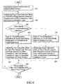
Figure 4 illustrates a flow chart of a detection method carried out in accordance with a first embodiment of the present invention; -
Figure 5 illustrates a flow chart of a detection method carried out in accordance with a second embodiment of the present invention; -
Figure 6 illustrates a system block diagram in accordance with another embodiment of the present invention; and -
Figure 7 is an exploded view illustrating a first conductive layer opposing a second conductive layer and spaced from each other by a plurality of insulation spacers when the first and second substrates ofFigure 6 arc assembled together. - With reference to the drawings and in particular to
Figure 1 , which illustrates a system block diagram of a touch control device in accordance with the present invention, the touch control device comprises a touch panel, which, generally designated at 100, comprises afirst substrate 1 and a second,opposite substrate 2. Thefirst substrate 1 has an under surface on which a firstconductive layer 10 is formed in a continuous planar structure. Thesecond substrate 2 has a top surface on which a secondconductive layer 20 is formed. Thefirst substrate 1 and thesecond substrate 2 are assembled together in a face-to-face manner with the firstconductive layer 10 opposing the secondconductive layer 20 and spaced from each other by a plurality of insulation spacers 21 (seeFigure 2 ). - The first
conductive layer 10 has opposite ends in a first direction X, which are respectively referred to as first end X1 and second end X2, both being electrically connected to acontrol circuit 3. - The second
conductive layer 20 comprises a plurality of elongate conductive strips Y1, Y2, Y3, ..., Yn, which are substantially parallel with but do not engage each other. Each elongate conductive strip Y1, Y2, Y3, ..., Yn is extended in a second direction Y on the top surface of thesecond substrate 2. - Each elongate conductive strip Y1, Y2, Y3, ..., Yn of the second
conductive layer 20 has a first end Y1a, Y2a, Y3a, ..., Yna and a second end Y1b, Y2b, Y3b, ..., Ynb, both being electrically connected to thecontrol circuit 3. - The
control circuit 3 is electrically connected to amicrocontroller 4 which controls the operation of thecontrol circuit 3 and receives signals from thecontrol circuit 3. - In
Figure 1 , the firstconductive layer 10 of thefirst substrate 1 and the elongate conductive strips Y1, Y2, Y3, ..., Yn of thesecond substrate 2, both constituting thetouch panel 100, can be replaced with each other so that thefirst substrate 1 is formed with a structure comprising a plurality of elongate conductive strips while thesecond substrate 2 provides a structure of continuous planar conductive layer. - For example, the first
conductive layer 10 of thetouch panel 100 is first used as a drive layer with the first end X1 of the firstconductive layer 10 being applied with a drive voltage V (such as 5V) by thecontrol circuit 3 and the second end X2 of the firstconductive layer 10 is controlled by thecontrol circuit 3 to connect to a predetermined voltage level, which can be ground voltage, zero voltage, or any fixed-value voltage, whereby a potential gradient is established in the firstconductive layer 10. When thetouch panel 100 is touched/depressed, the secondconductive layer 20 of thetouch panel 100 functions as a scan detection layer and thecontrol circuit 3 carries out scan detection on the secondconductive layer 20 sequentially through the first ends Y1a, Y2a, Y3a, ..., Yna of the elongate conductive strips Y1, Y2, Y3, ..., Yn of the secondconductive layer 20, or alternatively, scan detection is carried out sequentially through the first ends Y1a, Y2a, Y3a, ..., Yna and second ends Y1b, Y2b, Y3b, ..., Ynb of the elongate conductive strips Y1, Y2, Y3, ..., Yn, or further alternatively, scan detection is simultaneously performed at both ends of each elongate conductive strip Y1, Y2, Y3, ..., Yn but sequentially through all the elongate conductive strips Y1, Y2, Y3, ..., Yn. A variation of voltage in the secondconductive layer 20 is thus obtained and, based on such a variation of voltage, coordinates of a touch point can be calculated. - Then, the second
conductive layer 20 of thetouch panel 100 is used as the drive layer, whereby thecontrol circuit 3 applies a drive voltage V (such as 5V) to the first end Y1a, Y2a, Y3a, ..., Yna of each elongate conductive strip Y l, Y2, Y3, ..., Yn and the second ends Y1b, Y2b, Y3b, ..., Ynb of the elongate conductive strips Y1, Y2, Y3, ..., Yn arc controlled by thecontrol circuit 3 to connect to a predetermined voltage level, which can be ground voltage, zero voltage, or any fixed-value voltage, whereby a potential gradient is established in the secondconductive layer 20. The firstconductive layer 10 of thetouch panel 100 then functions as a scan detection layer and thecontrol circuit 3 performs detection on the firstconductive layer 10. A variation of voltage occurring in the firstconductive layer 10 can thus be obtained and, based on such a variation of voltage, coordinates of a touch position can be calculated. -
Figure 3 illustrates an equivalent circuit when two touch points on the elongate conductive strip Y1 are simultaneously touched/depressed. With simultaneous reference toFigure 1 , when the firstconductive layer 10 is subjected to touch at multiple points (such as touch points P1 and P2), the drive voltage V of the firstconductive layer 10 is applied to the elongate conductive strip Y1 of the secondconductive layer 20. When thecontrol circuit 3 performs scan detection on the first end Y1a of the elongate conductive strip Y1 (equivalent to the condition where switch S1 is closed and switch S2 is open), a detection voltage V1 = V x Rref1/(R1 + Rref1) is obtained at the first end Y1a of the elongate conductive strip Y1, where V is the provided preset drive voltage. When thecontrol circuit 3 performs scan detection on the second end Y1b of the elongate conductive strip Y1 (equivalent to the condition where switch S1 is open and switch S2 is closed), a detection voltage V2 = V x Rref2/(R2 + Rref2) is obtained at the second end Y1b of the elongate conductive strip Y1. In this way, the coordinates of the two touch points P1, P2 of touch on the elongate conductive strip Y1 can be simultaneously obtained. - Referring to
Figure 4 , which illustrates a flow chart of a detection method carried out in accordance with a first embodiment of the present invention, after system initialization of the touch control device is completed (step 101), themicrocontroller 4 initializes a preset scan detection mode to perform driving and scan detection respectively on the firstconductive layer 10 and the second conductive layer 20 (step 102). - The preset scan detection mode includes a first operation mode and a second operation mode. In practice, one of these two operation modes can be selected as the preset scan detection mode.
- When the first operation mode is selected as the preset scan detection mode, the following steps are carried out: The
control circuit 3 applies a drive voltage to the firstconductive layer 10 and carries out scan detection on at least one end of the first end Y1a, Y2a, Y3a, ..., Yna and the second end Y1b, Y2b, Y3b, ..., Ynb of each elongate conductive strip Y1, Y2, Y3, ..., Yn of the secondconductive layer 20. - When the second operation mode is selected as the preset scan detection mode, the following steps are carried out: The
control circuit 3 applies a drive voltage to the first end X1 of the firstconductive layer 10 and the second end X2 of the firstconductive layer 10 is controlled by thecontrol circuit 3 to connect to a preset voltage level, which can be ground voltage, zero voltage, or any fixed-value voltage, so as to establish a potential gradient in the firstconductive layer 10. At the same time, thecontrol circuit 3 carries out scan detection on at least one end of the first end Y1a, Y2a, Y3a, ..., Yna and the second end Y1b, Y2b, Y3b, ..., Ynb of each elongate conductive strip Y1, Y2, Y3, ..., Yn of the secondconductive layer 20. Thereafter, thecontrol circuit 3 applies a drive voltage to the first ends Y1a, Y2a, Y3a, ..., Yna of the secondconductive layer 20 and the second ends Y1b, Y2b, Y3b, ..., Ynb of the secondconductive layer 20 are controlled by thecontrol circuit 3 to connect to a preset voltage level, which can be ground voltage, zero voltage, or any fixed-value voltage, so as to establish a potential gradient in the secondconductive layer 20, and meanwhile, scan detection is carried out on the firstconductive layer 10. These steps are then repeated. - When a user touches the touch panel, the
microcontroller 4 determines the type of the touch operation (step 103). If it is determined that the type of touch operation applied to the touch panel is a single-point or a multiple-point touch (step 104), themicrocontroller 4 initializes the first operation mode to carry out respectively driving and scan detection on the firstconductive layer 10 and the secondconductive layer 20 to determine the coordinates of the touch point(s) (step 105). - If it is determined that the type of touch operation applied to the touch panel is an input of a continuous trace (step 106), the
microcontroller 4 initializes the second operation mode to carry out driving and scan detection on the firstconductive layer 10 and the secondconductive layer 20 to determine the coordinates of the continuous trace (step 107). - Finally, it is determined if the touch sustains for a given time period (step 108) and if yes, the process goes back to step 102, otherwise the process ends.
- In the
step 102 discussed above, when themicrocontroller 4 uses the preset scan detection mode to carry out driving and scan detection on the firstconductive layer 10 and the secondconductive layer 20 respectively, if the preset scan detection mode is the first operation mode, the coordinates of the single or multiple touch point(s) can be simultaneously obtained during the scan detection operation, and if the preset scan detection mode is the second operation mode, the coordinates of the continuous trace can be simultaneously obtained during the scan detection operation. - Referring to
Figure 5 , which illustrates a flow chart of an operation carried out in accordance with a second embodiment of the present invention, in the instant embodiment, after system initialization of the touch control device is completed (step 201), themicrocontroller 4 initializes a preset scan detection mode to per-form driving and scan detection respectively on the firstconductive layer 10 and the second conductive layer 20 (step 202). - The preset scan detection mode includes a first operation mode and a second operation mode. In practice, one of these two operation modes can be selected as the preset scan detection mode. The detailed operation flows associated with the first and second operation modes are identical to those of the first embodiment.
- When a user touches the touch panel, the
microcontroller 4 determines the type of the touch operation (step 203). If it is determined that the type of touch operation applied to the touch panel is a multiple-point touch (step 204), themicrocontroller 4 initializes the first operation mode to carry out driving and scan detection on the firstconductive layer 10 and the secondconductive layer 20 to determine the coordinates of the touch points (step 205). - If it is determined that the type of touch operation applied to the touch panel is a single-point touch or an input of a continuous trace (step 206), the
microcontroller 4 initializes the second operation mode to carry out driving and scan detection on the firstconductive layer 10 and the secondconductive layer 20 to determine the coordinates of the single touch point or the coordinates of the continuous trace (step 207). - Finally, it is determined if the touch sustains for a given time period (step 208) and if ycs, the process goes back to step 202, otherwise the process ends.
- In the
step 202 discussed above, when themicrocontroller 4 uses the preset scan detection mode to carry out driving and scan detection on the firstconductive layer 10 and the secondconductive layer 20 respectively, if the preset scan detection mode is the first operation mode, the coordinates of the multiple touch points can be simultaneously obtained during the scan detection operation, and if the preset scan detection mode is the second operation mode, the coordinates of the single touch point or those of the continuous trace can be simultaneously obtained during the scan detection operation. - Referring to
Figure 6 , which illustrates a system block diagram in accordance with a different embodiment from the touch control device ofFigure 1 , a touch panel, generally designated at 200, comprises afirst substrate 1 and a second,opposite substrate 2. Thefirst substrate 1 has an under surface on which a firstconductive layer 10a is formed. The firstconductive layer 10a comprises a plurality of elongate conductive strips X1', X2', X3', ..., Xn', which are substantially parallel with but do not engage each other. Each elongate conductive strip X1', X2', X3', ..., Xn' extends in a first direction X on the under surface of thefirst substrate 1. - The
second substrate 2 has a top surface on which a secondconductive layer 20 is formed. The secondconductive layer 20 comprises a plurality of elongate conductive strips Y1, Y2, Y3, ..., Yn, which arc substantially parallel with but do not engage each other. Each elongate conductive strip Y1, Y2, Y3, ..., Yn extends in a second direction Y on the top surface of thesecond substrate 2. - The first substrate I and the
second substrate 2 are assembled together with the firstconductive layer 10a opposing the secondconductive layer 20 and spaced from each other by a plurality of insulation spacers 21 (seeFigure 7 ). - Each elongate conductive strip X1', X2', X3', ..., Xn' of the first
conductive layer 10a has a first end X1a', X2a', X3a', ..., Xna' and a second end X1b', X2b', X3b', ..., Xnb', which are electrically connected to thecontrol circuit 3. - Each elongate conductive strip Y1, Y2, Y3, ..., Yn of the second
conductive layer 20 has a first end Y1a, Y2a, Y3a, ..., Yna and a second end Y1b, Y2b, Y3b, ..., Ynb, which are electrically connected to thecontrol circuit 3. - The system structure of this instant embodiment is similar to that of the embodiment illustrated in
Figure 1 and a significant difference is that thetouch panel 200 is considered an equivalent variation of thetouch panel 100 illustrated in the embodiment ofFigure 1 . The principle and steps of the operation of the instant embodiment are similar to those of the previously described embodiment and thus details thereof are omitted here for simplicity.
Claims (20)
- A touch position detection method for use in a touch control device that comprises a touch panel (100), the touch panel (100) comprising a first conductive layer (10) and a second conductive layer (20), the first conductive layer (10) comprising a continuous planar structure formed on a first substrate (1) and having first (X1) and second ends (X2), the second conductive layer (20) comprising a plurality of elongate conductive strips (Y1, Y2, Y3, ..., Yn) formed on a second substrate (2), the elongate conductive strips (Y1, Y2, Y3, ..., Yn) being substantially parallel to and not engaging each other, each elongate conductive strip (Y1, Y2, Y3, ..., Yn) having first (Y1a, Y2a, Y3a, ..., Yna) and second ends (Y1b, Y2b, Y3b, ..., Ynb), the first (1) and second substrates (2) being spaced from each other by insulation spacers (21), a control circuit (3) electrically connected to the first (10) and second conductive layers (20), and a microcontroller (4) electrically connected to the control circuit (3), characterized in that the method comprising the following steps:(a) the microcontroller (4) initializing a preset scan detection mode to carry out driving and scan detection on the first conductive layer (10) and the second conductive layer (20) through the control circuit (3);(b) when detecting a touch operation on the touch panel (100), determining if the type of touch applied to the touch panel (100) is multiple-point touch, continuous trace, or single-point touch;(c) when the type of touch being determined to be the single-point touch or multiple-point touch, the microcontroller (4) employing a first operation mode to carry out driving and scan detection on the first conductive layer (10) and the second conductive layer (20) to detect coordinates of a touch point/touch points;(d) when the type of touch being determined to be the continuous trace, the microcontroller (4) employing a second operation mode to carry out driving and scan detection on the first conductive layer (10) and the second conductive layer (20) to detect coordinates of the continuous trace;(c) determining if the touch operation sustains for a given time period; and(f) returning to step (a) when the touch operation sustains for the given time period.
- The method as claimed in Claim 1, characterized in that the first operation mode comprises the following steps:(c1) applying a drive voltage to the first conductive layer (10); and(c2) carrying out scan detection on at least one end of the first (Y I a, Y2a, Y3a, ..., Yna) and second ends (Y1b, Y2b, Y3b, ..., Ynb) of each elongate conductive strip (Y1, Y2, Y3, ..., Yn) of the second conductive layer (20).
- The method as claimed in Claim 1, characterized in that the second operation mode comprises the following steps:(d1) applying a drive voltage to the first end (X1) of the first conductive layer (10), the second end (X2) of the first conductive layer (10) being connected to a preset voltage level to thereby establish a potential gradient in the first conductive layer (10), and at the same time, carrying out scan detection on at least one end of the first (Y1a, Y2a, Y3a, ..., Yna) and second ends (Y1b, Y2b, Y3b, ..., Ynb) of each elongate conductive strip (Y1, Y2, Y3, ..., Yn) of the second conductive layer (20);(d2) applying a drive voltage to the first end (Y1a, Y2a, Y3a, ..., Yna) of each elongate conductive strip (Y1, Y2, Y3, ..., Yn) of the second conductive layer (20), the second end (Y1b, Y2b, Y3b, ..., Ynb) of each elongate conductive strip (Y1, Y2, Y3, ..., Yn) of the second conductive layer (20) being connected to a preset voltage level to thereby establish a potential gradient in the second conductive layer (20), and at the same time, carrying out scan detection on at least one end of the first (X1) and second ends (X2) of the first conductive layer (10).
- The method as claimed in Claim 1, characterized in that the preset scan detection mode is the first operation mode and characterized in that when the preset scan detection mode is the first operation modc, the coordinates of the single-point touch or the multiple-point touch are simultaneously obtained during the scan detection operation.
- The method as claimed in Claim 1, characterized in that the preset scan detection mode is the second operation mode.
- A touch position detection method for use in a touch control device that comprises a touch panel (100) comprising a first conductive layer (10) and a second conductive layer (20), the first conductive layer (10) comprising a continuous planar structure formed on a first substrate (1) and having first (X1) and second ends (X2), the second conductive layer (20) comprising a plurality of elongate conductive strips (Y1, Y2, Y3, ..., Yn) formed on a second substrate (2), the elongate conductive strips (Y1, Y2, Y3, ..., Yn) being substantially parallel to and not engaging each other, each elongate conductive strip (Y1, Y2, Y3, ..., Yn) having first (Y1a, Y2a, Y3a, ..., Yna) and second ends (Y1b, Y2b, Y3b, ..., Ynb), the first (1) and second substrates (2) being spaced from each other by insulation spacers (21), a control circuit (3) electrically connected to the first (10) and second conductive layers (20), and a microcontroller (4) electrically connected to the control circuit (3), the method comprising the following steps:(a) the microcontroller (4) initializing a preset scan detection mode to carry out driving and scan detection on the first conductive layer (10) and the second conductive layer (20) through the control circuit (3);(b) when detecting a touch operation applied to the touch panel (100), determining if the type of touch applicd to the touch panel (100) is single-point touch, multiple-point touch, or continuous trace;(c) when the type of touch being determined to be the multiple-point touch, the microcontroller (4) employing a first operation mode to carry out driving and scan detection on the first conductive layer (10) and the second conductive layer (20) to detect coordinates of touch point/touch points;(d) when the type of touch being determined to be the single-point touch or continuous trace, the microcontroller (4) employing a second operation mode to carry out driving and scan detection on the first conductive layer (10) and the second conductive layer (20) to detect coordinates of a touch point or coordinates of the continuous trace;(e) determining if the touch operation sustains for a given time period; and(f) returning to step (a) when the touch operation sustains for the given time period.
- The method as claimed in Claim 6, characterized in that the first operation mode comprises the following steps:(c1) applying a drive voltage to the first conductive layer (10); and(c2) carrying out scan detection on at least one end of the first (Y1a, Y2a, Y3a, ..., Yna) and second ends (Y1b, Y2b, Y3b, ..., Ynb) of each elongate conductive strip (Y1, Y2, Y3, ..., Yn) of the second conductive layer (20).
- The method as claimed in Claim 6, characterized in that the second operation mode comprises the following steps:(d1) applying a drive voltage to the first end (X1) of the first conductive layer (10), the second end (X2) of the first conductive layer (10) being connected to a preset voltage level to thereby establish a potential gradient in the first conductive layer (10), and at the same time, currying out scan detection on at least one end of the first (Y1a, Y2a, Y3a, ..., Yna) and second ends (Y1b, Y2b, Y3b, ..., Ynb) of each elongate conductive strip (Y1, Y2, Y3, ..., Yn) of the second conductive layer (20);(d2) applying a drive voltage to the first end (Y1a, Y2a, Y3a, ..., Yna) of each elongate conductive strip (Y1, Y2, Y3, ..., Yn) of the second conductive layer (20), the second end (Y1b, Y2b, Y3b, ..., Ynb) of each elongate conductive strip (Y1, Y2, Y3, ..., Yn) of the second conductive layer (20) being connected to a preset voltage level to thereby establish a potential gradient in the second conductive layer (20), and at the same time, carrying out scan detection on at least one end of the first (X1) and second ends (X2) of the first conductive layer (10).
- The method as claimed in Claim 6, characterized in that the preset scan detection mode is the first operation mode and characterized in that when the preset scan detection mode is the first operation mode, the coordinates of the multiple-point touch are simultaneously obtained during the scan detection operation.
- The method as claimed in Claim 6, characterized in that the preset scan detection mode is the second operation mode.
- A touch position detection method for use in a touch control device that comprises a touch panel (100) comprising a first conductive layer (10) and a second conductive layer (20), the first conductive layer (10a) having a plurality of elongate conductive strips (X1', X2', X3', ..., Xn') which are formed on a first substrate (1) and substantially parallel to and not engaging each other and each has a first end (X1a', X2a', X3a', ..., Xna') and a second end (X1b', X2b', X3b', ..., Xnb'), the second conductive layer (20) comprising a plurality of elongate conductive strips (Y1, Y2, Y3, ..., Yn) which is formed on a second substrate (2) and substantially parallel to and not engaging each other and each has first (Y1a, Y2a, Y3a, ..., Yna) and second ends (Y1b, Y2b, Y3b, ..., Ynb), the first (1) and second substrates (2) being spaced from each other by insulation spacers (21), a control circuit (3) electrically connected to the first (10a) and second conductive layers (20), and a microcontroller (4) electrically connected to the control circuit (3), the method comprising the following steps:(a) the microcontroller (4) initializing a preset scan detection mode to carry out driving and scan detection on the first conductive layer (10a) and the second conductive layer (20) through the control circuit (3);(b) when detecting a touch operation applied to the touch panel (100), determining if the type of touch applied to the touch panel (100) is multiple-point touch, continuous trace, or single-point touch;(c) when the type of touch being determined to be the single-point touch or multiple-point touch, the microcontroller (4) employing a first operation mode to carry out driving and scan detection on the first conductive layer (10a) and the second conductive layer (20) to detect coordinates of a touch point/touch points;(d) when the type of touch being determined to be the continuous trace, the microcontroller (4) employing a second operation mode to carry out driving and scan detection on the first conductive layer (10a) and the second conductive layer (20) to detect coordinates of the continuous trace;(e) determining if the touch operation sustains for a given time period; and(f) returning to step (a) when the touch operation sustains for the given time period.
- The method as claimed in Claim 11, characterized in that the first operation mode comprises the following steps:(c1) applying a drive voltage to each elongate conductive strip (X1', X2', X3', ..., Xn') of the first conductive layer (10a); and(c2) carrying out scan detection on at least one end of the first (Y1a, Y2a, Y3a, ..., Yna) and second ends (Y I b, Y2b, Y3b, ..., Ynb) of each elongate conductive strip (Y1, Y2, Y3, ..., Yn) of the second conducive layer (20).
- The method as claimed in Claim 11, characterized in that the second operation mode comprises the following steps:(d1) applying a drive voltage to the first end (X1a', X2a', X3a', ..., Xna') of each elongate conductive strip (X1', X2', X3', ..., Xn') of the first conductive layer (10a), the second end (X1b', X2b', X3b', ..., Xnb') of each elongate conductive strip (X1', X2', X3', ..., Xn') of the first conductive layer (10a) being connected to a preset voltage level to thereby establish a potential gradient in the first conductive layer (10a), and at the same time, carrying out scan detection on at least one end of the first (Y1a, Y2a, Y3a, ..., Yna) and second ends (Y1b, Y2b, Y3b, ..., Ynb) of each elongate conductive strip (Y1, Y2, Y3, ..., Yn) of the second conductive layer (20);(d2) applying a drive voltage to the first end (Y1a, Y2a, Y3a, ..., Yna) of each elongate conductive strip (Y1, Y2, Y3, ..., Yn) of the second conductive layer (20), the second end (Y1b, Y2b, Y3b, ..., Ynb) of each elongate conductive strip (Y1, Y2, Y3, ..., Yn) of the second conductive layer (20) being connected to a preset voltage level to thereby establish a potential gradient in the second conductive layer (20), and at the same time, carrying out scan detection on at least one end of the first (X1a', X2a', X3a', ..., Xna') and second ends (X1b', X2b', X3b', ..., Xnb') of each elongate conductive strip (X1', X2', X3', ..., Xn') of the first conductive layer (10a).
- The method as claimed in Claim 11, characterized in that the preset scan detection mode is the first operation mode and wherein when the preset scan detection mode is the first operation mode, the coordinates of the single-point touch or the multiple-point touch arc simultaneously obtained during the scan detection operation.
- The method as claimed in Claim 11, characterized in that the preset scan detection mode is the second operation mode.
- A touch position detection method for use in a touch control device that comprises a touch panel (100) comprising a first conductive layer (10a) and a second conductive layer (20), the first conductive layer (10a) having a plurality of elongate conductive strips (X1', X2', X3', ..., Xn') which are formed on a first substrate (1) and substantially parallel to and not engaging each other and each (X1', X2', X3', ..., Xn') has a first end (X1a', X2a', X3a', ..., Xna') and a second end (X1b', X2b', X3b', ..., Xnb'), the second conductive layer (20) comprising a plurality of elongate conductive strips (Y1, Y2, Y3, ..., Yn), which is formed on a second substrate (2) and substantially parallel to and not engaging each other and each has a first end (Y1a, Y2a, Y3a, ..., Yna) and a second end (Y1b, Y2b, Y3b, ..., Ynb), the first (I) and second substrates (2) being spaced from each other by insulation spacers (21), a control circuit (3) electrically connected to the first (10a) and second conductive layers (20), and a microcontroller (4) electrically connected to the control circuit (3), the method comprising the following steps:(a) the microcontroller (4) initializing a preset scan detection mode to carry out driving and scan detection on the first conductive layer (10a) and the second conductive layer (20) through the control circuit (3);(b) when detecting a touch operation applied to the touch panel (100), determining if the type of touch applied to the touch panel (100) is single-point touch, multiple-point touch, or continuous trace;(c) when the type of touch being determined to be the multiple-point touch, the microcontroller (4) employing a first operation mode to carry out driving and scan detection on the first conductive layer (10a) and the second conductive layer (20) to detect coordinates of touch point/touch points;(d) when the type of touch being determined to be the single-point touch or continuous trace, the microcontroller (4) employing a second operation mode to carry out driving and scan detection on the first conductive layer (10a) and the second conductive layer (20) to detect coordinates of a touch point or coordinates of the continuous trace;(e) determining if the touch operation sustains for a given time period; and(f) returning to step (a) when the touch operation sustains for the given time period.
- The method as claimed in Claim 16, characterized in that the first operation mode comprises the following steps:(c1) applying a drive voltage to each elongate conductive strip (X1', X2', X3', ..., Xn') of the first conductive layer (10a); and(c2) carrying out scan detection on at least one end of the first (Y1a, Y2a, Y3a, ..., Yna) and second ends (Y1b, Y2b, Y3b, ..., Ynb) of each elongate conductive strip (Y1, Y2, Y3, ..., Yn) of the second conductive layer (20).
- The method as claimed in Claim 16, characterized in that the second operation mode comprises the following steps:(d1) applying a drive voltage to the first end (X1a', X2a', X3a', ..., Xna') of each elongate conductive strip (X1', X2', X3', ..., Xn') of the first conductive layer (10a), the second end (X1b', X2b', X3b', ..., Xnb') of each elongate conductive strip (X1', X2', X3', ..., Xn') of the first conductive layer (10a) being connected to a preset voltage level to thereby establish a potential gradient in the first conductive layer (10a), and at the same time, carrying out scan detection on at least one end of the first (Y1a, Y2a, Y3a, ..., Yna) and second ends (Y1b, Y2b, Y3b, ..., Ynb) of each elongate conductive strip (Y1, Y2, Y3, ..., Yn) of the second conductive layer (20);(d2) applying a drive voltage to the first end (Y1a, Y2a, Y3a, ..., Yna) of each elongate conductive strip (Y1, Y2, Y3, ..., Yn) of the second conductive layer (20), the second end (Ylb, Y2b, Y3b, ..., Ynb) of each elongate conductive strip (Y1, Y2, Y3, ..., Yn) of the second conductive layer (20) being connected to a preset voltage level to thereby establish a potential gradient in the second conductive layer (20), and at the same time, carrying out scan detection on at least one end of the first (X1a', X2a', X3a', ..., Xna') and second ends (X1b', X2b', X3b', ..., Xnb') of each elongate conductive strip (X1', X2', X3', ..., Xn') of the first conductive layer (10a).
- The method as claimed in Claim 16, characterized in that the preset scan detection mode is the first operation mode and characterized in that when the preset scan detection mode is the first operation mode, the coordinates of the multiple-point touch are simultaneously obtained during the scan detection operation.
- The method as claimed in Claim 16, characterized in that the preset scan detection mode is the second operation mode.
Applications Claiming Priority (1)
| Application Number | Priority Date | Filing Date | Title |
|---|---|---|---|
| TW097137456A TW201013485A (en) | 2008-09-30 | 2008-09-30 | Touch-control position sensing method for a touch-control device |
Publications (2)
| Publication Number | Publication Date |
|---|---|
| EP2169519A1 true EP2169519A1 (en) | 2010-03-31 |
| EP2169519B1 EP2169519B1 (en) | 2013-03-27 |
Family
ID=40793192
Family Applications (1)
| Application Number | Title | Priority Date | Filing Date |
|---|---|---|---|
| EP09000218A Ceased EP2169519B1 (en) | 2008-09-30 | 2009-01-09 | Touch position detection method for touch control device |
Country Status (4)
| Country | Link |
|---|---|
| US (1) | US8274485B2 (en) |
| EP (1) | EP2169519B1 (en) |
| JP (1) | JP5268669B2 (en) |
| TW (1) | TW201013485A (en) |
Cited By (2)
| Publication number | Priority date | Publication date | Assignee | Title |
|---|---|---|---|---|
| CN102193863A (en) * | 2011-04-26 | 2011-09-21 | 青岛海信移动通信技术股份有限公司 | Method and device for implementing multi-point touch operation |
| CN102375585A (en) * | 2010-08-11 | 2012-03-14 | 普诚科技股份有限公司 | Method and touch device for detecting touch point of touch panel |
Families Citing this family (35)
| Publication number | Priority date | Publication date | Assignee | Title |
|---|---|---|---|---|
| US8508492B2 (en) * | 2009-01-19 | 2013-08-13 | Panasonic Corporation | Touch panel and method of detecting press operation position thereon |
| JP2010257444A (en) * | 2009-01-19 | 2010-11-11 | Panasonic Corp | Touch panel |
| JP2010186460A (en) * | 2009-01-19 | 2010-08-26 | Panasonic Corp | Touch panel |
| CN101833387B (en) * | 2009-03-13 | 2013-09-11 | 宸鸿光电科技股份有限公司 | Pressure sensitive touch device |
| TWI402738B (en) * | 2009-05-27 | 2013-07-21 | Wintek Corp | Touch apparatus and touch sensing method |
| US20110043462A1 (en) * | 2009-08-24 | 2011-02-24 | Ayman Shabra | Touchscreen apparatus, integrated circuit device, electronic device and method therefor |
| US8680390B2 (en) | 2009-10-16 | 2014-03-25 | Kesumo Llc | Foot-operated controller |
| KR20110055168A (en) * | 2009-11-19 | 2011-05-25 | 삼성전자주식회사 | A touch panel, a display device including the same, and a touch position sensing method of the touch panel |
| TWI434207B (en) | 2010-03-25 | 2014-04-11 | Novatek Microelectronics Corp | Touch sensing system, electronic touch apparatus, and touch sensing method |
| JP5450211B2 (en) * | 2010-04-01 | 2014-03-26 | ローム株式会社 | Touch panel control circuit, control method, touch panel input device using them, and electronic device |
| CN102214026B (en) * | 2010-04-06 | 2013-06-19 | 联咏科技股份有限公司 | Touch sensing system, electronic touch device and touch sensing method |
| US20110291950A1 (en) * | 2010-05-28 | 2011-12-01 | Research In Motion Limited | Electronic device including touch-sensitive display and method of controlling same |
| US9013441B2 (en) | 2010-08-24 | 2015-04-21 | Cypress Semiconductor Corporation | Smart scanning for a capacitive sensing array |
| TWI442280B (en) * | 2011-07-29 | 2014-06-21 | Acer Inc | Power saving method and touch display device |
| US9076419B2 (en) | 2012-03-14 | 2015-07-07 | Bebop Sensors, Inc. | Multi-touch pad controller |
| TWM442549U (en) * | 2012-05-23 | 2012-12-01 | Xuye Technology Co Ltd | Surface capacitive touch panel |
| CN103713780B (en) * | 2012-09-29 | 2017-12-26 | 联想(北京)有限公司 | The method and electronic equipment of a kind of information processing |
| TWI556144B (en) * | 2012-12-13 | 2016-11-01 | 奇景光電股份有限公司 | Method for determining position of touch event on touch panel and computer readable medium |
| US9766728B2 (en) | 2013-02-19 | 2017-09-19 | Himax Technologies Limited | Method for determining position of touch event on touch panel by dynamically adjusting threshold and related computer readable medium |
| EP2799966B1 (en) * | 2013-05-02 | 2022-10-26 | Siemens Aktiengesellschaft | Input device, control unit and method for detecting position |
| US9535519B1 (en) * | 2013-06-14 | 2017-01-03 | Google Inc. | Smart housing for extending trackpad sensing |
| US9965076B2 (en) | 2014-05-15 | 2018-05-08 | Bebop Sensors, Inc. | Piezoresistive sensors and applications |
| US9696833B2 (en) | 2014-05-15 | 2017-07-04 | Bebop Sensors, Inc. | Promoting sensor isolation and performance in flexible sensor arrays |
| US9753568B2 (en) | 2014-05-15 | 2017-09-05 | Bebop Sensors, Inc. | Flexible sensors and applications |
| US9442614B2 (en) * | 2014-05-15 | 2016-09-13 | Bebop Sensors, Inc. | Two-dimensional sensor arrays |
| US9710060B2 (en) | 2014-06-09 | 2017-07-18 | BeBop Senors, Inc. | Sensor system integrated with a glove |
| US10362989B2 (en) | 2014-06-09 | 2019-07-30 | Bebop Sensors, Inc. | Sensor system integrated with a glove |
| US9863823B2 (en) | 2015-02-27 | 2018-01-09 | Bebop Sensors, Inc. | Sensor systems integrated with footwear |
| US10082381B2 (en) | 2015-04-30 | 2018-09-25 | Bebop Sensors, Inc. | Sensor systems integrated with vehicle tires |
| US9827996B2 (en) | 2015-06-25 | 2017-11-28 | Bebop Sensors, Inc. | Sensor systems integrated with steering wheels |
| US9721553B2 (en) | 2015-10-14 | 2017-08-01 | Bebop Sensors, Inc. | Sensor-based percussion device |
| US10275078B1 (en) * | 2017-03-20 | 2019-04-30 | Rockwell Collins, Inc. | Split resistive touch sensor |
| US10884496B2 (en) | 2018-07-05 | 2021-01-05 | Bebop Sensors, Inc. | One-size-fits-all data glove |
| US11480481B2 (en) | 2019-03-13 | 2022-10-25 | Bebop Sensors, Inc. | Alignment mechanisms sensor systems employing piezoresistive materials |
| CN115963938A (en) * | 2021-10-09 | 2023-04-14 | 华为技术有限公司 | Method and device for displaying operation track |
Citations (5)
| Publication number | Priority date | Publication date | Assignee | Title |
|---|---|---|---|---|
| EP0487049A1 (en) * | 1990-11-20 | 1992-05-27 | Canon Kabushiki Kaisha | Electronic input device |
| US5181030A (en) | 1989-12-28 | 1993-01-19 | Gunze Limited | Input system including resistance film touch panel and pushed position detecting device |
| US5818430A (en) * | 1997-01-24 | 1998-10-06 | C.A.M. Graphics Co., Inc. | Touch screen |
| CN1503195A (en) | 2002-11-20 | 2004-06-09 | Lg.������Lcd��ʽ���� | Digital Resistive Touch Panel |
| US20050275634A1 (en) | 2004-06-15 | 2005-12-15 | International Business Machines Corportion | Resistive scanning grid touch panel |
Family Cites Families (9)
| Publication number | Priority date | Publication date | Assignee | Title |
|---|---|---|---|---|
| JPS59214941A (en) * | 1983-05-20 | 1984-12-04 | Toshiba Corp | Inputting device of position |
| JP2675454B2 (en) * | 1991-05-17 | 1997-11-12 | 沖電気工業株式会社 | Touch panel |
| JP3190407B2 (en) | 1992-02-27 | 2001-07-23 | グンゼ株式会社 | Touch panel device |
| US5982302A (en) * | 1994-03-07 | 1999-11-09 | Ure; Michael J. | Touch-sensitive keyboard/mouse |
| JP2000112642A (en) | 1998-09-30 | 2000-04-21 | Digital Electronics Corp | Touch panel |
| JP2001134382A (en) | 1999-11-04 | 2001-05-18 | Sony Corp | Graphic processing unit |
| US20080316182A1 (en) * | 2007-06-21 | 2008-12-25 | Mika Antila | Touch Sensor and Method for Operating a Touch Sensor |
| JP4915954B2 (en) * | 2007-11-27 | 2012-04-11 | グンゼ株式会社 | Touch panel and touch panel device using the touch panel |
| US20090322700A1 (en) * | 2008-06-30 | 2009-12-31 | Tyco Electronics Corporation | Method and apparatus for detecting two simultaneous touches and gestures on a resistive touchscreen |
-
2008
- 2008-09-30 TW TW097137456A patent/TW201013485A/en not_active IP Right Cessation
- 2008-12-30 US US12/318,487 patent/US8274485B2/en not_active Expired - Fee Related
-
2009
- 2009-01-09 EP EP09000218A patent/EP2169519B1/en not_active Ceased
- 2009-01-20 JP JP2009009744A patent/JP5268669B2/en not_active Expired - Fee Related
Patent Citations (5)
| Publication number | Priority date | Publication date | Assignee | Title |
|---|---|---|---|---|
| US5181030A (en) | 1989-12-28 | 1993-01-19 | Gunze Limited | Input system including resistance film touch panel and pushed position detecting device |
| EP0487049A1 (en) * | 1990-11-20 | 1992-05-27 | Canon Kabushiki Kaisha | Electronic input device |
| US5818430A (en) * | 1997-01-24 | 1998-10-06 | C.A.M. Graphics Co., Inc. | Touch screen |
| CN1503195A (en) | 2002-11-20 | 2004-06-09 | Lg.������Lcd��ʽ���� | Digital Resistive Touch Panel |
| US20050275634A1 (en) | 2004-06-15 | 2005-12-15 | International Business Machines Corportion | Resistive scanning grid touch panel |
Cited By (3)
| Publication number | Priority date | Publication date | Assignee | Title |
|---|---|---|---|---|
| CN102375585A (en) * | 2010-08-11 | 2012-03-14 | 普诚科技股份有限公司 | Method and touch device for detecting touch point of touch panel |
| CN102375585B (en) * | 2010-08-11 | 2014-04-09 | 普诚科技股份有限公司 | Method and touch device for detecting touch point of touch panel |
| CN102193863A (en) * | 2011-04-26 | 2011-09-21 | 青岛海信移动通信技术股份有限公司 | Method and device for implementing multi-point touch operation |
Also Published As
| Publication number | Publication date |
|---|---|
| US20100079389A1 (en) | 2010-04-01 |
| US8274485B2 (en) | 2012-09-25 |
| TWI376622B (en) | 2012-11-11 |
| JP2010086511A (en) | 2010-04-15 |
| JP5268669B2 (en) | 2013-08-21 |
| TW201013485A (en) | 2010-04-01 |
| EP2169519B1 (en) | 2013-03-27 |
Similar Documents
| Publication | Publication Date | Title |
|---|---|---|
| EP2169519B1 (en) | Touch position detection method for touch control device | |
| KR101685902B1 (en) | Touch sensing appratus and method for sensing approach | |
| KR100952017B1 (en) | Apparatus and method for scanning and detecting touch points of touch control panel | |
| EP2169518B1 (en) | Method for detecting touch points of touch control device | |
| US10025434B2 (en) | Touch system, touch panel, and display device | |
| CN102486708B (en) | touch panel | |
| US20100182278A1 (en) | Resistive touch control device and driving method and driving controller thereof | |
| KR100993907B1 (en) | Touch control device and method | |
| CN103257769A (en) | Capacitor-embedded touch screen and capacitor-embedded displaying device | |
| JP4935781B2 (en) | Information input device | |
| US20150185810A1 (en) | Touch screen device, touch screen display device using the same, and driving method thereof | |
| JPH11249813A (en) | Display-integrated coordinate input device | |
| CN101989143B (en) | Touch control device and control method thereof | |
| KR20180077394A (en) | Touch sensor, display device including the same, and operating method the touch sensor | |
| CN101727253B (en) | Touch position sensing method of touch device | |
| US10860158B2 (en) | Touch panel device, touch panel device control method, and non-transitory tangible computer-readable storage medium having the program stored therein | |
| JPH03171321A (en) | Input/output device | |
| JP5403905B2 (en) | Resistive touch panel | |
| KR101405164B1 (en) | Touch display apparatus | |
| US20200192503A1 (en) | Touch panel device, touch panel device control method, and non-transitory tangible computer-readable storage medium having the program stored therein | |
| JP5284768B2 (en) | Touch detection method of touch panel device | |
| CN101464768A (en) | Touch sensing method of touch device | |
| KR100456156B1 (en) | Apparatus And Method For Measuring Linearity Touch Panel | |
| JP2017199340A (en) | One-chip touch panel driving device, touch panel device including the same, and method for driving the same | |
| JP2012014683A (en) | Input device |
Legal Events
| Date | Code | Title | Description |
|---|---|---|---|
| PUAI | Public reference made under article 153(3) epc to a published international application that has entered the european phase |
Free format text: ORIGINAL CODE: 0009012 |
|
| 17P | Request for examination filed |
Effective date: 20090120 |
|
| AK | Designated contracting states |
Kind code of ref document: A1 Designated state(s): AT BE BG CH CY CZ DE DK EE ES FI FR GB GR HR HU IE IS IT LI LT LU LV MC MK MT NL NO PL PT RO SE SI SK TR |
|
| AX | Request for extension of the european patent |
Extension state: AL BA RS |
|
| 17Q | First examination report despatched |
Effective date: 20100504 |
|
| AKX | Designation fees paid |
Designated state(s): DE FR GB |
|
| GRAP | Despatch of communication of intention to grant a patent |
Free format text: ORIGINAL CODE: EPIDOSNIGR1 |
|
| GRAS | Grant fee paid |
Free format text: ORIGINAL CODE: EPIDOSNIGR3 |
|
| GRAA | (expected) grant |
Free format text: ORIGINAL CODE: 0009210 |
|
| AK | Designated contracting states |
Kind code of ref document: B1 Designated state(s): DE FR GB |
|
| REG | Reference to a national code |
Ref country code: GB Ref legal event code: FG4D |
|
| REG | Reference to a national code |
Ref country code: DE Ref legal event code: R096 Ref document number: 602009014315 Country of ref document: DE Effective date: 20130523 |
|
| REG | Reference to a national code |
Ref country code: DE Ref legal event code: R082 Ref document number: 602009014315 Country of ref document: DE Representative=s name: BOEHMERT & BOEHMERT, DE Ref country code: DE Ref legal event code: R082 Ref document number: 602009014315 Country of ref document: DE Representative=s name: BOEHMERT & BOEHMERT ANWALTSPARTNERSCHAFT MBB -, DE |
|
| PLBE | No opposition filed within time limit |
Free format text: ORIGINAL CODE: 0009261 |
|
| 26N | No opposition filed |
Effective date: 20140103 |
|
| REG | Reference to a national code |
Ref country code: DE Ref legal event code: R097 Ref document number: 602009014315 Country of ref document: DE Effective date: 20140103 |
|
| REG | Reference to a national code |
Ref country code: FR Ref legal event code: PLFP Year of fee payment: 8 |
|
| REG | Reference to a national code |
Ref country code: FR Ref legal event code: PLFP Year of fee payment: 9 |
|
| REG | Reference to a national code |
Ref country code: FR Ref legal event code: PLFP Year of fee payment: 10 |
|
| PGFP | Annual fee paid to national office [announced via postgrant information from national office to epo] |
Ref country code: FR Payment date: 20211125 Year of fee payment: 14 Ref country code: GB Payment date: 20211118 Year of fee payment: 14 |
|
| PGFP | Annual fee paid to national office [announced via postgrant information from national office to epo] |
Ref country code: DE Payment date: 20211116 Year of fee payment: 14 |
|
| REG | Reference to a national code |
Ref country code: DE Ref legal event code: R119 Ref document number: 602009014315 Country of ref document: DE |
|
| GBPC | Gb: european patent ceased through non-payment of renewal fee |
Effective date: 20230109 |
|
| PG25 | Lapsed in a contracting state [announced via postgrant information from national office to epo] |
Ref country code: GB Free format text: LAPSE BECAUSE OF NON-PAYMENT OF DUE FEES Effective date: 20230109 Ref country code: DE Free format text: LAPSE BECAUSE OF NON-PAYMENT OF DUE FEES Effective date: 20230801 |
|
| PG25 | Lapsed in a contracting state [announced via postgrant information from national office to epo] |
Ref country code: FR Free format text: LAPSE BECAUSE OF NON-PAYMENT OF DUE FEES Effective date: 20230131 |