EP2166826A2 - A package for power converters with improved transformer operations - Google Patents
A package for power converters with improved transformer operations Download PDFInfo
- Publication number
- EP2166826A2 EP2166826A2 EP09016073A EP09016073A EP2166826A2 EP 2166826 A2 EP2166826 A2 EP 2166826A2 EP 09016073 A EP09016073 A EP 09016073A EP 09016073 A EP09016073 A EP 09016073A EP 2166826 A2 EP2166826 A2 EP 2166826A2
- Authority
- EP
- European Patent Office
- Prior art keywords
- pcb
- electronic
- power
- circuit board
- multilayer circuit
- Prior art date
- Legal status (The legal status is an assumption and is not a legal conclusion. Google has not performed a legal analysis and makes no representation as to the accuracy of the status listed.)
- Granted
Links
Images








Classifications
-
- H—ELECTRICITY
- H05—ELECTRIC TECHNIQUES NOT OTHERWISE PROVIDED FOR
- H05K—PRINTED CIRCUITS; CASINGS OR CONSTRUCTIONAL DETAILS OF ELECTRIC APPARATUS; MANUFACTURE OF ASSEMBLAGES OF ELECTRICAL COMPONENTS
- H05K1/00—Printed circuits
- H05K1/16—Printed circuits incorporating printed electric components, e.g. printed resistors, capacitors or inductors
- H05K1/165—Printed circuits incorporating printed electric components, e.g. printed resistors, capacitors or inductors incorporating printed inductors
-
- H—ELECTRICITY
- H01—ELECTRIC ELEMENTS
- H01F—MAGNETS; INDUCTANCES; TRANSFORMERS; SELECTION OF MATERIALS FOR THEIR MAGNETIC PROPERTIES
- H01F27/00—Details of transformers or inductances, in general
- H01F27/06—Mounting, supporting or suspending transformers, reactors or choke coils not being of the signal type
-
- H—ELECTRICITY
- H05—ELECTRIC TECHNIQUES NOT OTHERWISE PROVIDED FOR
- H05K—PRINTED CIRCUITS; CASINGS OR CONSTRUCTIONAL DETAILS OF ELECTRIC APPARATUS; MANUFACTURE OF ASSEMBLAGES OF ELECTRICAL COMPONENTS
- H05K1/00—Printed circuits
- H05K1/02—Details
- H05K1/0201—Thermal arrangements, e.g. for cooling, heating or preventing overheating
- H05K1/0203—Cooling of mounted components
- H05K1/0204—Cooling of mounted components using means for thermal conduction connection in the thickness direction of the substrate
- H05K1/0206—Cooling of mounted components using means for thermal conduction connection in the thickness direction of the substrate by printed thermal vias
-
- H—ELECTRICITY
- H05—ELECTRIC TECHNIQUES NOT OTHERWISE PROVIDED FOR
- H05K—PRINTED CIRCUITS; CASINGS OR CONSTRUCTIONAL DETAILS OF ELECTRIC APPARATUS; MANUFACTURE OF ASSEMBLAGES OF ELECTRICAL COMPONENTS
- H05K7/00—Constructional details common to different types of electric apparatus
- H05K7/20—Modifications to facilitate cooling, ventilating, or heating
- H05K7/2089—Modifications to facilitate cooling, ventilating, or heating for power electronics, e.g. for inverters for controlling motor
- H05K7/209—Heat transfer by conduction from internal heat source to heat radiating structure
-
- H—ELECTRICITY
- H05—ELECTRIC TECHNIQUES NOT OTHERWISE PROVIDED FOR
- H05K—PRINTED CIRCUITS; CASINGS OR CONSTRUCTIONAL DETAILS OF ELECTRIC APPARATUS; MANUFACTURE OF ASSEMBLAGES OF ELECTRICAL COMPONENTS
- H05K1/00—Printed circuits
- H05K1/02—Details
- H05K1/0201—Thermal arrangements, e.g. for cooling, heating or preventing overheating
- H05K1/0203—Cooling of mounted components
-
- H—ELECTRICITY
- H05—ELECTRIC TECHNIQUES NOT OTHERWISE PROVIDED FOR
- H05K—PRINTED CIRCUITS; CASINGS OR CONSTRUCTIONAL DETAILS OF ELECTRIC APPARATUS; MANUFACTURE OF ASSEMBLAGES OF ELECTRICAL COMPONENTS
- H05K1/00—Printed circuits
- H05K1/02—Details
- H05K1/03—Use of materials for the substrate
- H05K1/05—Insulated conductive substrates, e.g. insulated metal substrate
-
- H—ELECTRICITY
- H05—ELECTRIC TECHNIQUES NOT OTHERWISE PROVIDED FOR
- H05K—PRINTED CIRCUITS; CASINGS OR CONSTRUCTIONAL DETAILS OF ELECTRIC APPARATUS; MANUFACTURE OF ASSEMBLAGES OF ELECTRICAL COMPONENTS
- H05K2201/00—Indexing scheme relating to printed circuits covered by H05K1/00
- H05K2201/06—Thermal details
- H05K2201/066—Heatsink mounted on the surface of the printed circuit board [PCB]
-
- H—ELECTRICITY
- H05—ELECTRIC TECHNIQUES NOT OTHERWISE PROVIDED FOR
- H05K—PRINTED CIRCUITS; CASINGS OR CONSTRUCTIONAL DETAILS OF ELECTRIC APPARATUS; MANUFACTURE OF ASSEMBLAGES OF ELECTRICAL COMPONENTS
- H05K2201/00—Indexing scheme relating to printed circuits covered by H05K1/00
- H05K2201/08—Magnetic details
- H05K2201/083—Magnetic materials
- H05K2201/086—Magnetic materials for inductive purposes, e.g. printed inductor with ferrite core
-
- H—ELECTRICITY
- H05—ELECTRIC TECHNIQUES NOT OTHERWISE PROVIDED FOR
- H05K—PRINTED CIRCUITS; CASINGS OR CONSTRUCTIONAL DETAILS OF ELECTRIC APPARATUS; MANUFACTURE OF ASSEMBLAGES OF ELECTRICAL COMPONENTS
- H05K2201/00—Indexing scheme relating to printed circuits covered by H05K1/00
- H05K2201/09—Shape and layout
- H05K2201/09009—Substrate related
- H05K2201/09054—Raised area or protrusion of metal substrate
-
- H—ELECTRICITY
- H05—ELECTRIC TECHNIQUES NOT OTHERWISE PROVIDED FOR
- H05K—PRINTED CIRCUITS; CASINGS OR CONSTRUCTIONAL DETAILS OF ELECTRIC APPARATUS; MANUFACTURE OF ASSEMBLAGES OF ELECTRICAL COMPONENTS
- H05K2201/00—Indexing scheme relating to printed circuits covered by H05K1/00
- H05K2201/09—Shape and layout
- H05K2201/09009—Substrate related
- H05K2201/09063—Holes or slots in insulating substrate not used for electrical connections
-
- H—ELECTRICITY
- H05—ELECTRIC TECHNIQUES NOT OTHERWISE PROVIDED FOR
- H05K—PRINTED CIRCUITS; CASINGS OR CONSTRUCTIONAL DETAILS OF ELECTRIC APPARATUS; MANUFACTURE OF ASSEMBLAGES OF ELECTRICAL COMPONENTS
- H05K2201/00—Indexing scheme relating to printed circuits covered by H05K1/00
- H05K2201/09—Shape and layout
- H05K2201/09209—Shape and layout details of conductors
- H05K2201/095—Conductive through-holes or vias
- H05K2201/09572—Solder filled plated through-hole in the final product
-
- H—ELECTRICITY
- H05—ELECTRIC TECHNIQUES NOT OTHERWISE PROVIDED FOR
- H05K—PRINTED CIRCUITS; CASINGS OR CONSTRUCTIONAL DETAILS OF ELECTRIC APPARATUS; MANUFACTURE OF ASSEMBLAGES OF ELECTRICAL COMPONENTS
- H05K2201/00—Indexing scheme relating to printed circuits covered by H05K1/00
- H05K2201/09—Shape and layout
- H05K2201/09209—Shape and layout details of conductors
- H05K2201/09654—Shape and layout details of conductors covering at least two types of conductors provided for in H05K2201/09218 - H05K2201/095
- H05K2201/09745—Recess in conductor, e.g. in pad or in metallic substrate
-
- H—ELECTRICITY
- H05—ELECTRIC TECHNIQUES NOT OTHERWISE PROVIDED FOR
- H05K—PRINTED CIRCUITS; CASINGS OR CONSTRUCTIONAL DETAILS OF ELECTRIC APPARATUS; MANUFACTURE OF ASSEMBLAGES OF ELECTRICAL COMPONENTS
- H05K2201/00—Indexing scheme relating to printed circuits covered by H05K1/00
- H05K2201/10—Details of components or other objects attached to or integrated in a printed circuit board
- H05K2201/10007—Types of components
- H05K2201/10166—Transistor
-
- H—ELECTRICITY
- H05—ELECTRIC TECHNIQUES NOT OTHERWISE PROVIDED FOR
- H05K—PRINTED CIRCUITS; CASINGS OR CONSTRUCTIONAL DETAILS OF ELECTRIC APPARATUS; MANUFACTURE OF ASSEMBLAGES OF ELECTRICAL COMPONENTS
- H05K3/00—Apparatus or processes for manufacturing printed circuits
- H05K3/0058—Laminating printed circuit boards onto other substrates, e.g. metallic substrates
- H05K3/0061—Laminating printed circuit boards onto other substrates, e.g. metallic substrates onto a metallic substrate, e.g. a heat sink
-
- Y—GENERAL TAGGING OF NEW TECHNOLOGICAL DEVELOPMENTS; GENERAL TAGGING OF CROSS-SECTIONAL TECHNOLOGIES SPANNING OVER SEVERAL SECTIONS OF THE IPC; TECHNICAL SUBJECTS COVERED BY FORMER USPC CROSS-REFERENCE ART COLLECTIONS [XRACs] AND DIGESTS
- Y10—TECHNICAL SUBJECTS COVERED BY FORMER USPC
- Y10T—TECHNICAL SUBJECTS COVERED BY FORMER US CLASSIFICATION
- Y10T29/00—Metal working
- Y10T29/49—Method of mechanical manufacture
- Y10T29/49002—Electrical device making
- Y10T29/49117—Conductor or circuit manufacturing
- Y10T29/49124—On flat or curved insulated base, e.g., printed circuit, etc.
- Y10T29/49155—Manufacturing circuit on or in base
- Y10T29/49165—Manufacturing circuit on or in base by forming conductive walled aperture in base
Definitions
- This invention relates generally to the electrical design and mechanical packaging of electronic components, and more particularly to a method of power conversion utilizing a multiple transformers primaries in series and secondary in parallel.
- One approach to packaging electric components in power converters includes a housing which both encloses the components and means of heat extraction from the components.
- the house includes a non-conductive casing 5 and an aluminum heat-sinking base.
- a printed circuit board (PCB) 3 is mounted next to the upper wall 5a of the casing.
- Conductive pins 7 are attached directly to the PCB 3 and extend up through the wall 5a.
- Electronic components 9a, 9c are mounted to one or both sides of the PCB 3. Larger side components such as the transformer 9c are monted to the lower side for space reason.
- Power dissipating devices such as 9b are mounted directly on the base-plate 6,for better heat transfer.
- the power components 9b are electrically connected to the PBC by leads 12.
- Structure 1 may be filled with an encapsulant, which acts as a heat spreader and provides mechanical support. In the case when a hard epoxy encapsulant is used a"buffer coating" material is used to protect some of the components.
- This invention is related to the electrical design and mechanical packaging of electronic components. It involves a new method of power conversion utilizing a multiple transformers primaries in series and secondary in parallel (or vice versa).
- a transformer group is created in which a multitude of transformers are used to supply energy to a single load.
- the transformers are connected in series; in order to assist in providing a "flux equalizing" affect, the invention includes a flux equalizer circuit.
- the flux equalizer circuit provides a series of flux windings. Each flux winding is associated with a single transformer. The windings are arranged in a closed loop. In this manner, a balancing of the output of the transformers is obtained; the flux swing from each transformer is "sensed" by its associated flux winding which is “shared” with the other transformers via their own associated load winding.
- the invention provides a packaging technology for power converters and power magnetics.
- the packaging methodology provides a compact, inexpensive, easy to manufacture.
- the invention features a package for electrical components held on a circuit board.
- most of the power magnetic elements are constructed into the multilayers PCD.
- the windings of the magnetic elements such as transformer, inductors, and in some cases event signal transformers are incorporated in the multilayers PCB.
- the top layer and some portion of the bottom layer are also support for electronic components.
- the windings of the magnetic elements are contained inside of the multilayers PCB; the electronic components are placed on the top and on the bottom of the PCB. Some of the components are located on top of the windings and the interconnections between the magnetic elements.
- the footprint of the magnetic elements is reduced to the footprint of the transformer core.
- the power-dissipating devices replaced on pads, which have a multitude of copper coated via to the other side of the PCB.
- the heat transferred to the other side of the PCB can be further spread using a larger pad or transferred to a metallic base-plate attached to the PCB through an isolating material.
- an additional heat sink is attache to the heat spreader to increase its cooling area.
- the unique aspect of this packaging concept is the fact that the magnetic element's windings are incorporated on the multilayers PCB construction which also serves as a support for power-dissipating components and some of the control components.
- the heat from the power-dissipating components is extracted through copper coated via which transfer the heat to the other side of the PCB.
- the heat is further transferred to a metal base plate connected to the PCB via a thermally conductive insulator.
- the heat spreader connected to the thermal via can serve as a cooling surface.
- a heatsink can be also attached to the heat spreader to increased the heat dissipation area.
- figure 1 illustrates the prior art of this invention.
- a power-dissipating electronic components 22 are located on the multilayer PCB 28 on top of the heat spreader pad 18, Fig 4B .
- the heat spreader pad is connected to the copper coated via.
- a heat spreader 74, Fig 4B is connected on the backside of the PCB through the copper coated via 42.
- the copper coated via can be filled with solder or can be empty in which case the heat will be transferred through the metalization placed on the wall of the via.
- the metalization is formed by copper deposit during the plating process associated with the manufacturing process of the PCB. As a result of the plating process the wall of the via is covered with copper.
- the via can be also filled with a thermally conductive material 30a as is presented in figure 4D .
- the isolated material 30 placed under the PCB 28 under pressure will penetrate through the via filling the space.
- an insulator material with good thermal conductivity characteristics 30 is placed in between the 28 and the metal base plate 32 .
- the heat from the power dissipating components 22 is transferred through the copper pad 48 on which the power dissipating device is mounted, to the copper coated via 42 to the other side of the PCB, 28B, to the heat spreader 74.
- the heat is further transferred through the thermally conductive insulator material 30 to the metal plate 32.
- the thermally conductive insulator material 30 will penetrate through the copper coated via 12 the surface contact will increase and as a result the thermal transfer from the copper pad 48 to the metal plate 30 will be improved.
- the main embodiments of this invention is the magnetic elements implementation in the multilayers PCD and the means in which the heat is extracted form the power dissipating devices, from the magnetic winding 50, ( Figure 3A and Fig 3B ), from the magnetic core 26A and 26B, and the low power dissipation devices 20 to the baseplate 32.
- some components 88 are mounted on top of the multilayers PCB 28a, on top of the windings 50 embedded in the inner layers of the multilayers PCB 28. In this way the footprint of the magnetic element is reduced to the footprint of the magnetic core 26a.
- the main embodiment of this invention is the fact that the magnetics elements are implemented in the multilayers PCB 28.
- the magnetic elements were discrete devices which were connected to the PCD by means of through hole or surface mounted pins.
- the presence of the connecting pins increases the coast of the magnetic element and it reduces the reliability of the magnetic device due to the mechanical failure of the pins.
- the interconnection pin can be bent or broken easily.
- the presence of the interconnection pins adds supplementary stray inductance in series with the transformer. This will negatively impact the electrical performance of the circuit. In most of the applications the energy contained in this parasitic inductance is dissipated, reducing the parasitic inductance of the inter connection pins can increase to voltage or current stress on the electrical components.
- the magnetic elements have the windings embedded inside of the multilayers PCB.
- the interconnection between the magnetic elements and between the magnetic elements and the electronic components are made through copper pads etched in the layers of the multilayers PCB and through the copper coated via 42 in the multiyear PCB 28. This allows the use of more complex winding arrangements and allows the use of more magnetic elements on the same multilayers PCB construction.
- the interconnections of these magnetic elements are made within the multilayer PCB.
- the converter will contain a number of smaller magnetic elements achieving a low profile package.
- the magnetic cores 26A and 26b will penetrate through multilayers PCB via the cutouts 78a and 78b fitted for the outer legs 80a and inner legs 80b.
- the magnetic sections 26a and 26b can be glued together or attached via a spring clips 82. To accommodate the spring clip additional cutouts in the PCB 84 are produced. The bottom side of the magnetic core 26b, will surface on the back of the PCB. To be able to accommodate the magnetic cores 26b cutouts 86 are made through the insulator material 30. In most of applications the thickness of the insulator material is smaller than the height of the magnetic core. To accommodate the magnetic core 26b, cavities 56, are produced into the base plate 32. Due to the fragile characteristic of the magnetic cores, a soft pad 56, with small thermal impedance is placed under the magnetic core 26b in the cavity. The pad 56, will dampen the vibration of the magnetic core, The low thermal impedance of the pad 56, will also offer a cooling path for the magnetic core. In some applications wherein insulation has to be achieved to the base plate, the pad, 56 have to have insulation properties.
- the entire structure 7 is press together in a way that the magnetic core 26b will be placed on top of the pad 56.
- the thickness of the pad has to chosen in a way that the metallic plate 32 makes good contact with the insulator 30.
- the insulator 30, is pressed between the PCB 28 and metal plate 32.
- the permanent attachment can be done in several ways.
- the isolator material 30 has adhesive properties stimulated by a curing process at higher temperature. After the curing process the insulator created a bound between the PCB 28, and the metal plate 32.
- the flanges 40 can accommodate screws.
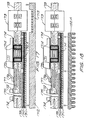
- FIG. 4C A cross-section of the structure 7, mounted is presented in Fig. 4C .
- FIG. 4B A section of the structure is blown in figure 4B .
- the cross-section of the structure 90 is presented the location of a power dissipation device on top of the copper pad 48, and the coated via 42.
- the copper coated via carry the heat to the heat spreader 74.
- the heat is further transferred via the thermally conductive insulator 30 to the metal plate 32.
- a second cross-section of the mounted structure 7, is presented in figure 4C .
- the cross-section, 92 is presented the upper section of the magnetic core 26a, the bottom section of the magnetic core 26b, the pad under the magnetic core 34 located in the cavity 56.
- the heat generated in the magnetic core 26 is transferred to the base plate through the pad 34.
- copper coated via are placed under the components or to the traces and pad connected to the components. In this way low thermal impedance is achieved to the base plate. With low thermal impedance to the base plate, the temperature rise of these components will be small.
- Using screws, clips, or different means of applying pressure to the structure 7 can also make the attachment of the PCB 28, to the isolator 30 and the base-plate 32.
- the cutouts in the metallic plate 32 can penetrate through the plate.
- the magnetic cores 26b will be visible from the bottom side of the metallic plate.
- soft epoxy material can cover the remaining cavity in between the magnetic core and the surface of the base plate 32. In some application that cavity can be left open.
- FIG 8 is presented a structure 9 wherein the package 7 is attached to a motherboard 96. The attachment is done through the power connectors 24a and 24b. The power connectors are attached to the motherboard 96 through screws 98. There is a signal connector 106 located on the structure 7. The signal connector 106 is connected to the matching signal connector 104 located on motherboard 96. More than one structure 7 can be connected to the same motherboard 96. On the motherboard 96 there are additional components 100 and 102. This structure it is suitable for systems wherein only the power train and some control functions are located on the structure 7. Some of the control section components, supplementary logic circuits and EMI filters are located on the motherboard. The bottom layer of the motherboard 96 may contain copper shields to protect the noise sensitive components. The noise sensitive components are located on the motherboard and the power dissipate components, some control components and the magnetics are located on the structure 7.
- FIG 5a and 5b is presented a packaging structure 11.
- the magnetic element has its winding embedded within the multilayers PCB 28 as it is in structure 7.
- the components are located on both sides of the multilayers PCB.
- This packaging structure applies to low power dissipation application wherein there is an airflow.
- the entire surface of multilayers PCB 28 becomes a heatsink.
- the structure 11 is connected to the other circuitry via the pins 52.
- FIG 7A is depicted a power system which contains several packaging structures 15.
- the structure 15 include the magnetic elements 26, the power dissipating components 22, the low power dissipation components 20, similar with structure 7.
- the main difference is that there is not an isolator 30, and a base plate 32.
- the cooling is accomplished by the air, which flows in between the packaging structures 15.
- the entire surface of 15 becomes a heatsink.
- the structures 15 are connected to the motherboard 64 through signal connectors 70a, and power connectors 70b.
- the motherboard 64 is connected to two packaging structures 17. These packaging structures contain the same components as structure 15 with an additional heat sink 58 attached to the multilayers PCB 28 through the insulator 30.
- FIG 6A and ⁇ B Two types of heatsink construction are presented in figure 6A and ⁇ B.
- the heatsink 58 has air fins 60 and cavities 62.
- a soft compressible material 34, with low thermal impedance is placed in the cavities .
- the insulator with low thermal impedance 30 is placed between the multilayers PCB 28 and the base plate 58.
- the magnetic core 26b is cooled via the soft pad 34.
- the power-dissipation devices are cooled though copper coated via like in structure 7.
- the heatsink 58 with air fins 60 has cutout-outs 64 to accommodate for the magnetic core 26b.
- the cooling of the magnetic core 26a and 26b is accomplished by the airflow.
- the cooling of the power-dissipation devices is done through copper coated via 42.
- FIG 9 is presented a packaging structure wherein the metal plate 32 does not contain cavities. It has elevated sections 104, which makes contact with the thermally conductive insulator 30, which is placed under the multilayers PCB 28.
- the elevated sections of the metal plate 104 are primarily placed under the power dissipated devices 22 and other low dissipation components 20c which require to have a temperature close to the base plate temperature.
- the thermally conductive soft pad 34, on the base plate 32 supports the magnetic core 26a and 26b.
- the height of the elevated section of the baseplate 104 are function of the height of the magnetic core 26b and the compression ratio of the pad 34.
- the advantage of the packaging concept is the fact that more components can be mounted on the multilayers PCB on the backside 20b. This package is suitable for power converters, which contains all the control and signal interface functions.
- the interconnection pins 24a and 24b will provide the power and signal connections to the outside word.
- the cover 106 contains holes 110 to accommodate the interconnection pins 24a and
- teeth 112 are formed along the lower edge of the case.
- a matching grove 108 is undercut into the base plate 32.
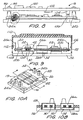
- FIG 10A is presented a high power magnetic structure wherein the magnetic core is formed by several small magnetic cores 26.
- a cross-section through the structure 19 is presented in figure 10B .
- the windings 50 of the magnetic structure are embedded in the multilayer PCB layers.
- the cutout 116 in the multilayers PBC 28 are made to accommodate the magnetic cores 26.
- Power connectors are inserted in the multilayers PBC 28.
- the connectors 24a and 24b are connected to the windings 50.
- the cores 26a and 26b are attached together via the clips 82.
- the multilayers PCB 28 wherein the windings 50 are embedded into also offers supports for the magnetic cores 26.
- a cavity 56 is placed in the base plate 32.
- a thermally conductive soft pad is placed under the magnetic core 26b on top of base plate 32.
- Figure 11 is an electrical schematic of the preferred embodiment of the multiple transformer using flux equalizing loops.
- the source for the primary is an AC source 111.
- L PN multiple primaries denoted L PN which are connected in series.
- the transformer is optionally a discrete type of transformer which is soldered to the PCB or it is constructed of windings embedded in a multilayer PCB with an E-cores.
- the present invention provides for a balancing the output power needs between the multiple secondaries.
- an auxiliary secondary winding (112A, 112B) is added to each transformer in such a way to balance the flux densities between the transformers.
- These secondary windings are denoted L B1 - L BN and are connected together in parallel as shown in figure 1 .
- currents flow in this secondary winding to force the flux densities in the transformers to be equal.
- Current sharing in this way accounts for differences in device characteristics between the different power trains which is desirable.
- Figure 12 is an electrical schematic of an alternative embodiment of the multiple transformer invention in which no central taps have been utilized.
- figure 12 performs in an identical manner as that of figure 11 , except that in the figure 12 embodiment, the transformers do not have a central tap.
- Figure 13 is an electrical schematic of an embodiment of the multiple transformer invention in which the flux equalizing loops react to electrical flow through multiple power trains. These multiple power trains can be phase shifted to reduce the input and output current ripple.
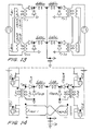
- Figure 14 is an electrical schematic of an alternative embodiment of the multiple transformer invention.
- auxiliary windings Laux1 and Laux2 are connected in parallel with reverse polarity to insure a bi-directional flux swing in the transformers.
- Figure 15 is a method of implementing a flux equalizing loop.
- Layer 151A and 151B are two different layers of a multi-layered printed circuit board. Magnet core 152 extends through the multi-layered printed circuit board. Other magnet cores 155 and 154 are also positioned through the PCB. Copper layer 153A is used to create the flux windings; flux windings created by copper layer 153B is offset to create the required phase shift.
- Figure 16 is an electrical schematic of an embodiment in which flux equalizing loops are employed also in the output choke.
- the flux equalizing loops L B1 ... L BN will ensure an equal flux swing in the transformer T R1 ... T RN .
- the flux equalizing loops L ofL ... L ofL will ensure equal flux swing in the output inductance elements L 01 ...L 0N for stead state and dynamic operating conditions.
- the coupling between L 01 ...L 0N and L of1 and L ofN can be loose, without deviating from the scope of this invention.
- Figure 17 shows a cross-sectional diagram of the completed PCB assembly using the improved thermal coupling apparatus for this invention.
- the basic components for this embodiment are: power device 171 other devices 172, magnetic cores 173, solder 174, via with plated copper walls 175, legs of the power device 176, inner layers 177, printed circuit board (PCB) having multilayers 178, copper foil 179, insulation material 1710, metal plate1711, additional heat sink 1712, compressible thermoconductive material 1713, and metal insert 1714.
- PCB printed circuit board
- Electrical components (171, 172 and 173) are assembled on a multilayer PCB (178). Under the power device (171) are one or more multiple vias (175) which are plated with copper. Vias 175 are large enough to accept a large metal insert (1714) which is soldered to the PCB. These metal inserts are much better thermal conductors than solder alone.
- the thermal insert/ plug 1714 used within the via has thermal conductivity properties improved over solder.
- the thermal conductivity of the plug is at least 25 percent greater than solder.
- Thermal conductivity is the heat flow across a surface per unit time, divided by the negative of the rate of change of temperature with distance in a direction perpendicular to the surface.
- the top layer is a thin copper foil (179).
- a portion of this copper foil (179) is soldered to the under side of the PCB in the location where the metal inserts (1714) protrude through the PCB. Electrical isolation from the rest of the foil is provided by cutting a small island in the this location which is to be soldered to the metal inserts (1714).
- the rest of the copper foil (179) is not soldered to the bottom of the PCB, it relies on pressure to provide the coupling for heat transfer.
- the middle layer of the substrate (1710) is a thermally conducting material which electrically insulates the copper foil layer from the bottom aluminum plate (1711).
- the PCB along with the substrate may then be mounted to an aluminum baseplate (1712).
- Any conductive devices such as ferrite cores (1713) may be electrically isolated from the baseplate by means of a compressible thermoconductive material.
- the method of operation for this system is to solder the power device to the top of the PCB, on top of the soldered metal inserts.
- the heat generated during electrical operation of the circuit is easily transmitted through the metal inserts.
- the heat is spread out over a large surface area through the insulation material to the aluminum plate and to the baseplate.
- the power device 171 is optionally a die placed on the metal insert 1714 and with bond wire connected to the multilayer PCB.
- Figure 18 illustrates an embodiment of the invention which utilizes an additional heatsink.
- electrical components (171, 172 and 173) are assembled on a multilayer PCB (178). Under the power device (171) there are multiple vias (175) which are plated with copper.
- an insulated multilayer substrate which aids in the transfer of heat from the PCB to the aluminum heatsink.
- This substrate is comprised of three different materials.
- the top layer is a thin copper foil (179). A portion of this copper foil (179) is soldered to the under side of the PCB (178) in the location where the metal insert protrude through the PCB (178).
- the middle layer of the substrate (1710) is a thermally conducting material which electrically insulates the copper foil layer from the bottom aluminum plate conducting material which electrically insulates the copper foil layer from the bottom aluminum plate (1711).
- the PCB along with the substrate is then be mounted to an aluminum heatsink (182A).
- the method of operation for this system is to solder the power device to the top of the PCD above the soldered metal inserts.
- the heat generated during electrical operation of the circuit is transmitted through the metal inserts to the copper foil island underneath. This island is large compared to the metal inserts to allow for greater thermal conductivity.
- the heat is spread out over a large surface area through the insulation material to the aluminum plate and to the heatsink.
- the size of the copper foil layer 179 underneath the metal insert is tailored to control the capacitance between the power device 171 and heat sink1712.
- Figure 19 is still another embodiment of the invention in which the thermal slugs/inserts are wedged into the via.
- the metal inserts/slugs194A are also unique in that they have a small through hole 1715 which extends from its top to bottom. This allows for a good solder flow due to a capillary action when the insert is soldered from a portion of the underlying multilayer substrate to the power device on top side of the PCB.
- the metal inserts/slugs 194A have a diameter greater than the diameter of the via with its walls coated with copper.
- the PCB along with the substrate is mounted to an aluminum baseplate (1712).
- Any conductive devices such as ferrite cores (173) may be electronically isolated from the baseplate by means of compressible thermoconductive material.
- the method of operation for this system is to solder the power device to the top of the PCB, on top of the pressure fitted metal inserts.
- the heat generated during electrical operation of the circuit is transmitted through the metal inserts so there is no decrease in the thermal resistivity of this junction.
- the heat is spread out over a large surface area through the insulation material to the aluminum plate and to the baseplate.
- Figure 20 is still another embodiment of the thermal conductive aspect of this invention.
- the embodiment of figure 20 includes the electrical components (171, 172 and 173) are assembled on a multilayer PCB (178).
- the metal inserts (194A) have a small through hole 174A which extends from its top to bottom. This allows for a good solder flow due to a capillary action when the insert is soldered from a portion of the underlying multilayer substrate to the power device on the top side of the PCB (178).
- the substrate is located directly underneath the PCB and its function is to aid in the transfer of heat from the PCD to the aluminum heatsink.
- This substrate is comprised of three different materials.
- the top layer is a thin copper foil (179).
- the PCB along with the substrate is mounted to an aluminum heatsink (182A).
- the method of manufacture for this system is to solder the power device to the top of the PBC, on top of the pressure fitted metal inserts (194A).
- the heat generated during electrical operation of the circuit is transmitted through the metal inserts (194A).
- the heat generated during electrical operation of the circuit is transmitted through the metal inserts to the copper foil island underneath. This island is large compared to the metal inserts so there is no decrease in the thermal resistivity of this junction.
- the heat is spread out over a large surface area through the insulation material to the aluminum plate and to the baseplate.
- Figure 21 illustrates an alternative embodiment in which the metal slugs extend past the PCB and are used to secure the heatsink to the PCB.
- metal inserts/slug 214C have a length sufficient to extend through the PCB and also through holes 216 of heat sink 1712.
- the PCB assembly is mounted to an aluminum baseplate (1712), acting as a heatsink, which has holes (216) to accompany the metal inserts (214C).
- a tight pressure fit is required for good thermal transfer.
- Any conductive devices such as ferrite cores (173) or smaller electrical vias (175) may be electrically isolated from the base plate by means of a compressible thermoconductive material.
- Manufacture of this embodiment is to solder the power device to the top of the PCB, on top of the pressure fitted metal inserts. The heat generated during electrical operation of the circuit is transmitted through the metal inserts directly to the aluminum baseplate underneath.
- Metal insert/slug 1713C have a contoured exterior wall to allow liquid solder to flow therebetween to provide for bonding and also for electrical conductivity.
- Figure 22 illustrates an embodiment of the invention having enhanced cooling capabilities.
- metal inserts/slugs (214C) are elongated to pass through PCB (178) and engage cooling vane 182B.
- the embodiment of figure 22 uses metal inserts/slugs 214C which mechanically engage the walls of vias (174) and the holes 216 within the cooling vane 182.
- Metal insert/slug 214C have a contoured exterior wall to allow liquid solder to flow therebetween to provide for bonding and also for electrical conductivity.
- figure 23 is presented the preferred embodiment of the invention.
- a multilayer PCB which incorporates the winding of the magnetic element 2316.
- a magnetic core 2310 of the magnetic element 2316 is constructed in the multilayer PCB 232.
- the high frequency switching electronic components 238, which is connected to the magnetic element 2316 with minimum insertion impedance are also located on the multilayer PCB 232.
- the interconnection between the magnetic element 2316 and the high frequency switching electronic components 238 shall be made to minimize the parasitic inductance and with minimum impedance insertion.
- the rest of the electronic components 236 of the electronic circuit are located on the mother PCB, 234 that can contain a reduced number of layers and as a result is lower cost.
- the rest of the electronic components which are processing lower frequency signals can be located on the mother PCB.
- FIG 25A is presented the magnetic element 2310, with the high frequency switching electronic components 238 and the interconnection pads 2350.
- FIG 25B is presented one of the embodiments of this patent referring to the method of attachment of attachment of the power PCB, 232, containing the magnetic element 16, and the mother PCB, 234.
- the power PCB 232 contains copper coated via 2524, which allow the penetration of the solder 2522B.
- the solder 2522B creates a medium for current flow and also constitutes a mechanical bind between power PCB 232, and the mother PCB 234.
- the melted solder 2522B, during the soldering process will spread in between 254B and 2552D and will further penetrate through 2524, creating a mechanical bound, and a path for current and heat flow.
- figure 25C is presented another embodiment of the invention wherein the interconnection between 232 and 234 is accomplished with the pin 2526C pressed in power PCB 232, and further soldered to 234.
- FIG 25D the attachment between 232 and 234 is accomplished with the use of a pressed insert 2530D,
- the pressed insert has to be made from a conductive material, to create not only a bond but also a path for current and heat.
- figure 25E is presented another embodiment of the invention wherein the surface mounted pin 2510E is used as interconnection between 232 and 234.
- the surface mounted pin 2510E has to be electrically and thermally conductive to allow an efficient current and heat flow between 232 and 234.
- FIG 25F is presented another embodiment of the invention wherein the interconnection between 232 and 231 is provided by the pressed connectors 260F and 280F and a screw 282F.
- the pressed connector 260F is pressed fit in the mother PCB 234 and the pressed connector 280F is pressed fit in the power PCB 232.
- the screw 282F ensures a bond between 280F and 260F.
- the pressed inserts 260F and 280F should be also very good conductors for current and heat to create a very low electrical and thermal impedance path between 232 and 234.
- FIG 26 is presented an embodiment of the invention wherein components 2612, are located ont he bottom side of the mother PCB.
- components 2612 are located ont he bottom side of the mother PCB.
- an additional metal plate 2726 is attached to the mother PCB 234, via a dielectric material 2724. In this way the heat can be extracted from the mother PCB to the metal plate 2726 which acts as a heatsink.
- FIG 27B is presented another embodiment of the invention wherein a isolated metal substrate element composed by a metal plate 2734, a dielectric 2732 and copper foil 2730, is attached to the mother PCB. Additional electric components 2728 can be attached to the copper pads, edged on the copper foil 2730.
- This packaging method allows the heat transfer from the power PCB 232, and mother PCB 234, to be transferred to the metal plate 2734.
- the location of additional components as 2728, leads to an increased in power density.
- Figure 27C presents an embodiment of the invention in which the magnetic element 2316 is attached to an isolated metal substrate composed of a dielectric material 2732, copper foil 2752, and metal plate 2734.
- a cutout 2700 in the isolated metal substrate is performed to accommodate the magnetic core 2310.
- the interconnection between the isolated metal substrate and the magnetic element 2316 is made via the copper foil 2752 and via 2724. In the soldering process, the melted solder penetrates through via 2724, creating an electrical and mechanical bind.
- the advantage of this embodiment is the fact that high power dissipating devices are located directly on the isolated metal substrate with very low thermal impedance to the metal plate 2734.
- the magnetic core 2310 penetrates through, power PCB 232, and mother PCB, 234.
- the windings 2318 created in the layers of the power PCB 232, and the windings 2819 created in the mother PCB 234, can be magnetically coupled . In this way it is increased the level of utilization of the mother PCB 234.
- figure 29 there are two power PCB linked magnetically through core 2310 with the mother PCB 234.
- This symmetrical structure can offer some advantages such as interleaving the primary and secondary winding of the magnetic structure using the magnetic core 2310.
- FIG 30 there are high frequency switching electronic components located on both power PCB.
- the primary winding of the transformer element using the magnetic core 2310 can be located on the mother PCB 234, the secondary winding can be implemented in the power PCB 232 and 232B and the additional high frequency switching electronic components such as rectifiers means can be surface mounted on 232 and 232B.
- an additional metal plate 316 is attached to at he power PCB 232, via a dielectric material 314.
- the heat produced by the magnetic element 2316, with winding 2318 and magnetic core 2310, and by the high frequency switching electronic components 238 can be transferred to 316 and further transferred to air or additional heatsink.
- figure 32 is presented similar concept as in figure 31 , wherein some of the high frequency switching electronic components is located under the metal plate 316B.
- the metal plate 316B has cavities to accommodate the components 238A placed on top of the power PCB 232
- the high power dissipation electronic components 330 are located on an alumina substrate 332.
- the interconnection between the alumina substrate 332 and the power PCB 232 is provided by the pins 338.
- the module created by the power PCB with the high frequency switching electronic components 238, 330 the metal plate 336 is attached to the mother PCB 232.
- the advantage of this concept is the fact that it offers a good thermal path from the high heat dissipation components to a metal plate heatsink 336.
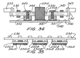
- the high heat dissipation components as 340 are located on top of a heat conductive insert 344.
- the insert is further penetrating into a copper interface 342.
- the copper interface 342 is soldered to the copper foil 341 located on the dielectric 346, attached to a metal plate 348.
- the mechanical structure formed by 344, 342, 341 can efficiently extract the heat from the device 340 to the metal plate 348. This mechanical structure can also efficiently be a path for the current flow.
- the power processing module formed by power PCB 234, high frequency switching electronic components such as 238 and 340, the thermal interface 344, 342, 341, dielectric layer 346 and the metal plate 348, can be further connected to the mother PCB 232
- each power PCB contains at least one magnetic element and the high frequency switching electronic components.
- the rest of the electronic components, such as the signal control portion are located on the mother PCB 234.
- Cooling plates 316A... 316Z can be further attached to the power PCB for cooling.
- the high frequency switching electronic components and high heat dissipation components are located on the power PCB, separated from the rest of electronic components located on mother PCB, 234.
- the high power dissipation components which in most of the power converters are also high frequency switching electronic components, are separated by the noise and heat sensitive components located on the mother PCB.
- the size of high cost, large number of layers power PCB is reduced, leading to a low cost design.
- the high frequency switching high power dissipation electronic components are separated by the rest of the components leading to improve electrical-thermal characteristics.
- This packaging concept offers also increased flexibility.
- the number of power PCB, which includes magnetic elements and high frequency switching electronic components, can increase to increase the output power.
- the present invention creates a highly improved transformer package which provides for the enhanced provision of power with the burden properly split between the transformers.
Landscapes
- Engineering & Computer Science (AREA)
- Microelectronics & Electronic Packaging (AREA)
- Power Engineering (AREA)
- Physics & Mathematics (AREA)
- Thermal Sciences (AREA)
- Dc-Dc Converters (AREA)
- Coils Or Transformers For Communication (AREA)
- Surgical Instruments (AREA)
- Automatic Cycles, And Cycles In General (AREA)
- Discharge Heating (AREA)
- Coils Of Transformers For General Uses (AREA)
- Transformers For Measuring Instruments (AREA)
Abstract
a) an electronic board (234) having an opening therein, said electronic board (234) further including two pads (2552B) positioned on a first surface of said electronic board (234) proximate to said opening;
b) a multilayer circuit board (232) having secured thereto a transformer, said multilayer circuit board (232) positioned such that a portion of a first surface of said multilayer circuit board (232) engages the first surface of said electronic board (234) such that a portion of a core (2310) of said transformer extends into the opening of said electronic board (234), said multilayer circuit board (232) having at least two channels (2524) there through, each of said channels (2524) aligned with one of said at least two pads (2552B) of said electronic board (234); and
c) solder (2522) extending through said at least two channels (2524) in said multilayer circuit board (232), said solder (2522) bonded to the channel (2524) and to an associated pad (254B) on said electronic board (234).

Description
- This invention relates generally to the electrical design and mechanical packaging of electronic components, and more particularly to a method of power conversion utilizing a multiple transformers primaries in series and secondary in parallel.
- One approach to packaging electric components in power converters (
Fig. 1 ) includes a housing which both encloses the components and means of heat extraction from the components. The house includes a non-conductive casing 5 and an aluminum heat-sinking base. A printed circuit board (PCB) 3 is mounted next to theupper wall 5a of the casing.Conductive pins 7 are attached directly to thePCB 3 and extend up through thewall 5a. Electronic components 9a, 9c are mounted to one or both sides of thePCB 3. Larger side components such as the transformer 9c are monted to the lower side for space reason. Power dissipating devices such as 9b are mounted directly on the base-plate 6,for better heat transfer. The power components 9b are electrically connected to the PBC byleads 12. Some of the power dissipating devices, 9d, are attached to the base plate via a thermallyconductive insulator material 8.Structure 1 may be filled with an encapsulant, which acts as a heat spreader and provides mechanical support. In the case when a hard epoxy encapsulant is used a"buffer coating" material is used to protect some of the components. - In the multiple transformer configuration of this invention, the use of multiple transformers is not new. These multiple secondaries (parallel or not) provide for equal currents but these currents get constricted in the rectifiers and output chokes. Using this type of structure requires large, expensive output chokes and special high current rectifiers which take up precious PCB space. Another drawback to the standard topology is that as device characteristics change over time in the rectifiers and transformers, the currents in the secondaries become more unbalanced while adversely affecting the flux densities in the transformers.
- It is clear that there is a need for an improved circuit for multiple transformer systems.
- This invention is related to the electrical design and mechanical packaging of electronic components. It involves a new method of power conversion utilizing a multiple transformers primaries in series and secondary in parallel (or vice versa).
- Within the present invention, a transformer group is created in which a multitude of transformers are used to supply energy to a single load. The transformers are connected in series; in order to assist in providing a "flux equalizing" affect, the invention includes a flux equalizer circuit. The flux equalizer circuit provides a series of flux windings. Each flux winding is associated with a single transformer. The windings are arranged in a closed loop. In this manner, a balancing of the output of the transformers is obtained; the flux swing from each transformer is "sensed" by its associated flux winding which is "shared" with the other transformers via their own associated load winding.
- As background, the invention provides a packaging technology for power converters and power magnetics. The packaging methodology provides a compact, inexpensive, easy to manufacture. The invention features a package for electrical components held on a circuit board. In this packaging concept most of the power magnetic elements are constructed into the multilayers PCD. The windings of the magnetic elements such as transformer, inductors, and in some cases event signal transformers are incorporated in the multilayers PCB. The top layer and some portion of the bottom layer are also support for electronic components. The windings of the magnetic elements are contained inside of the multilayers PCB; the electronic components are placed on the top and on the bottom of the PCB. Some of the components are located on top of the windings and the interconnections between the magnetic elements. In this way the footprint of the magnetic elements is reduced to the footprint of the transformer core. The power-dissipating devices replaced on pads, which have a multitude of copper coated via to the other side of the PCB. The heat transferred to the other side of the PCB can be further spread using a larger pad or transferred to a metallic base-plate attached to the PCB through an isolating material. For air-cooled due to the limited surface of the heat spreader, an additional heat sink is attache to the heat spreader to increase its cooling area.
- The unique aspect of this packaging concept is the fact that the magnetic element's windings are incorporated on the multilayers PCB construction which also serves as a support for power-dissipating components and some of the control components. The heat from the power-dissipating components is extracted through copper coated via which transfer the heat to the other side of the PCB. The heat is further transferred to a metal base plate connected to the PCB via a thermally conductive insulator. For airflow cooling applications the heat spreader connected to the thermal via can serve as a cooling surface. A heatsink can be also attached to the heat spreader to increased the heat dissipation area.
- In the multiple transformer configuration of this invention, in order to ensure that the flux level is kept proper for each of the transformers, another secondary winding is added to each transformer to force that the flux densities in each transformer to be equal. In addition, the outputs are paralleled after the output chokes so the currents are spread over multiple secondaries each complete with their own rectifiers and output chokes.
- The invention, together with various embodiments thereof, will be more fully explained by the accompanying drawings and the following descriptions.
-
-
Figure 1 is a cross-sectional side view of prior art components packaging. -
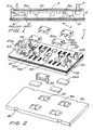
Figure 2 is a perspective exploded view of component packaging according to the invention. -
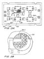
Figure 3A is a top view of the packaging with a detailed section of the magnetic' winding. -
Figure 3B is an enlarged view of a section ofFig 3A -
Figure 4A is a top view of the packaging with a detailed section of the cooling via. -
Figure 4C is a section of the packaging through the cooling via and through a magnetic element. -
Figure 4D is a broken view of the cooling via herein the insulator material penetrates in the cooling via. -
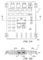
Figure 5A is the top view of the horizontal packaging with airflow cooling. -
Figure 5B is a cross section of the embodiment offigure 5A . -
Figure 6 is a top view of the packaging -
Figure 6A is a cross-section of the package with cooling by airflow and cavities for magnetic cores. -
Figure 6B is a cross-section of the package with cooling by airflow and holes for magnetic cores. -
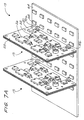
Figure 7A it is a perspective view of the power packages for airflow cooling. -
Figure 7B is a perspective view of the power packages for airflow cooling and additional heating applied to the multilayers circuit board. -
Figure 8 is a cross-section of the packaging connected to the motherboard. -
Figure 9 it is another embodiment of the present invention. -
Figure 10A is a high power magnetics package according to this invention. -
Figure 10B is a cross-section of the magnetic package presented infigure 10 . -
Figure 11 is an electrical schematic of the preferred embodiment of the multiple transformer using flux equalizing loops. -
Figure 12 is an electrical schematic of an alternative embodiment of the multiple transformer invention in which no central taps have been utilized. -
Figure 13 is an electrical schematic of an embodiment of the multiple transformer invention in which the flux equalizing loops react to electrical flow through multiple power trains. -
Figure 14 is an electrical schematic of an alternative embodiment of the multiple transformer invention. -
Figure 15 is a method of implementing the flux equalizing loops of this invention. -
Figure 16 is an electrical schematic of an embodiment in which the flux equalizing loops are employed also in the output choke. -
Figure 17 shows a cross-sectional diagram of the completed PCB assembly using the improved thermal coupling apparatus for this invention. -
Figure 18 illustrates an embodiment of the invention which utilizes an additional heatsink. -
Figure 19 is still another embodiment of the invention in which the thermal slugs/inserts are wedged into the via. -
Figure 20 is still another embodiment of the thermal conductive aspect of this invention. -
Figure 21 illustrates an alternative embodiment in which the metal slugs extend past the PCB and are used to secure the heatsink to the PCB. -
Figure 22 illustrates an embodiment of the invention having enhanced cooling capabilities. -
Figure 23 presents a multilayer PCB which contain the magnetic element and the high frequency switching electronic components of the electronic circuit. -
Figure 24 presents the criteria used to define the high frequency switching electronic components. -
Figure 25A presents the multilayer PCB structure that incorporates the magnetic element and the high frequency electronic components. -
Figure 25B presents a method of attaching the power PCB to the mother PCB using copper coated via and solder penetrating through copper coated via. -
Figure 25C presents a method of attaching the power PCD to the mother PCB using through hole pins. -
Figure 25D presents a method of attaching the power PCB to the mother PCB using a pressed insert. -
Figure 25E presents a method of attaching the power PCB to the mother PCB using surface mounted pins. -
Figure 25F presents a method of attaching the power PCB to the mother PCB using two pressed inserts and a screw. -
Figure 26 presents the same structure depicted infigure 11 wherein surface mounted components are placed on both side of the mother PCB. -
Figure 27A presents the same structure depictedfigure 11 wherein a cooling plate is attached to the mother PCB. -
Figure 27B presents the same structure depicted infigure 15A wherein the cooling plate is replaced by an isolated metal substrate, wherein surface mounted components are placed in the space between power PCB and isolated metal substrate. -
Figure 27C presents an embodiment wherein the magnetic element is attached to an isolated metal substrate composed by a dielectric material, copper foil, and metal plate. -
Figure 28 presents another embodiment of this invention wherein the magnetic core goes through both the power PCB and the mother PCB. -
Figure 29 presents another embodiment of this invention wherein the magnetic core goes through several PCB. -
Figure 30 presents another embodiment of this invention wherein the magnetic core goes through several power PCB which contain high frequency switching electronic components and through the mother PCB. -
Figure 31 presents another embodiment of this invention wherein a metal plate is attached to the power PCB. -
Figure 32 presents another embodiment of this invention wherein a metal plate with cavities to accommodate some of the high frequency switching electronic components are attached to the power PCB. -
Figure 33 presents another embodiment of this invention wherein some of the high heat dissipation components are located on an alumina substrate placed on a metal plate. -
Figure 34 presents another embodiment of this invention wherein the high heat dissipation components are located on top of a thermally conductive insert further soldered to a copper foil edged on an isolated metal substrate board. -
Figure 35 presents another embodiment of the invention wherein the power PCB, the high frequency switching electronic components for power processing cells, which can be multiplied to meet the power requirements. - As described before,
figure 1 , illustrates the prior art of this invention. - Referring to
Fig 2 in thepackaging 7 provided by this invention, a power-dissipatingelectronic components 22 are located on themultilayer PCB 28 on top of theheat spreader pad 18,Fig 4B . The heat spreader pad is connected to the copper coated via. A heat spreader 74,Fig 4B , is connected on the backside of the PCB through the copper coated via 42. The copper coated via can be filled with solder or can be empty in which case the heat will be transferred through the metalization placed on the wall of the via. The metalization is formed by copper deposit during the plating process associated with the manufacturing process of the PCB. As a result of the plating process the wall of the via is covered with copper. The via can be also filled with a thermallyconductive material 30a as is presented infigure 4D . Theisolated material 30 placed under thePCB 28 under pressure will penetrate through the via filling the space. In between the 28 and themetal base plate 32 an insulator material with goodthermal conductivity characteristics 30 is placed. In this way the heat from thepower dissipating components 22, is transferred through thecopper pad 48 on which the power dissipating device is mounted, to the copper coated via 42 to the other side of the PCB, 28B, to the heat spreader 74. The heat is further transferred through the thermallyconductive insulator material 30 to themetal plate 32. In the case wherein theinsulator material 30 will penetrate through the copper coated via 12 the surface contact will increase and as a result the thermal transfer from thecopper pad 48 to themetal plate 30 will be improved. - The main embodiments of this invention is the magnetic elements implementation in the multilayers PCD and the means in which the heat is extracted form the power dissipating devices, from the magnetic winding 50, (
Figure 3A and Fig 3B ), from the magnetic core 26A and 26B, and the lowpower dissipation devices 20 to thebaseplate 32. To increase the power density, some components 88 are mounted on top of the multilayers PCB 28a, on top of thewindings 50 embedded in the inner layers of themultilayers PCB 28. In this way the footprint of the magnetic element is reduced to the footprint of themagnetic core 26a. - The main embodiment of this invention is the fact that the magnetics elements are implemented in the
multilayers PCB 28. In the prior art the magnetic elements were discrete devices which were connected to the PCD by means of through hole or surface mounted pins. The presence of the connecting pins increases the coast of the magnetic element and it reduces the reliability of the magnetic device due to the mechanical failure of the pins. The interconnection pin can be bent or broken easily. The presence of the interconnection pins adds supplementary stray inductance in series with the transformer. This will negatively impact the electrical performance of the circuit. In most of the applications the energy contained in this parasitic inductance is dissipated, reducing the parasitic inductance of the inter connection pins can increase to voltage or current stress on the electrical components. - In this invention the magnetic elements have the windings embedded inside of the multilayers PCB. The interconnection between the magnetic elements and between the magnetic elements and the electronic components are made through copper pads etched in the layers of the multilayers PCB and through the copper coated via 42 in the
multiyear PCB 28. This allows the use of more complex winding arrangements and allows the use of more magnetic elements on the same multilayers PCB construction. The interconnections of these magnetic elements are made within the multilayer PCB. The converter will contain a number of smaller magnetic elements achieving a low profile package. Themagnetic cores 26A and 26b will penetrate through multilayers PCB via thecutouts 78a and 78b fitted for theouter legs 80a and inner legs 80b. Themagnetic sections PCB 84 are produced. The bottom side of themagnetic core 26b, will surface on the back of the PCB. To be able to accommodate themagnetic cores 26b cutouts 86 are made through theinsulator material 30. In most of applications the thickness of the insulator material is smaller than the height of the magnetic core. To accommodate themagnetic core 26b,cavities 56, are produced into thebase plate 32. Due to the fragile characteristic of the magnetic cores, asoft pad 56, with small thermal impedance is placed under themagnetic core 26b in the cavity. Thepad 56, will dampen the vibration of the magnetic core, The low thermal impedance of thepad 56, will also offer a cooling path for the magnetic core. In some applications wherein insulation has to be achieved to the base plate, the pad, 56 have to have insulation properties. - The
entire structure 7 is press together in a way that themagnetic core 26b will be placed on top of thepad 56. The thickness of the pad has to chosen in a way that themetallic plate 32 makes good contact with theinsulator 30. Theinsulator 30, is pressed between thePCB 28 andmetal plate 32. The permanent attachment can be done in several ways. In the preferred embodiment theisolator material 30 has adhesive properties stimulated by a curing process at higher temperature. After the curing process the insulator created a bound between thePCB 28, and themetal plate 32. In applications wherein thestructure 28 is connected to anther plate, theflanges 40 can accommodate screws. - A cross-section of the
structure 7, mounted is presented inFig. 4C . A section of the structure is blown infigure 4B . In the cross-section of the structure 90 is presented the location of a power dissipation device on top of thecopper pad 48, and the coated via 42. The copper coated via carry the heat to the heat spreader 74. The heat is further transferred via the thermallyconductive insulator 30 to themetal plate 32. - A second cross-section of the mounted
structure 7, is presented infigure 4C . In the cross-section, 92, is presented the upper section of themagnetic core 26a, the bottom section of themagnetic core 26b, the pad under themagnetic core 34 located in thecavity 56. The heat generated in themagnetic core 26 is transferred to the base plate through thepad 34. For components which have to have a temperature close to the temperature of the base plate, copper coated via are placed under the components or to the traces and pad connected to the components. In this way low thermal impedance is achieved to the base plate. With low thermal impedance to the base plate, the temperature rise of these components will be small. - Using screws, clips, or different means of applying pressure to the
structure 7 can also make the attachment of thePCB 28, to theisolator 30 and the base-plate 32. In some applications the cutouts in themetallic plate 32 can penetrate through the plate. Themagnetic cores 26b will be visible from the bottom side of the metallic plate. For protecting themagnetic cores 26b, soft epoxy material can cover the remaining cavity in between the magnetic core and the surface of thebase plate 32. In some application that cavity can be left open. - In
figure 8 is presented a structure 9 wherein thepackage 7 is attached to amotherboard 96. The attachment is done through thepower connectors 24a and 24b. The power connectors are attached to themotherboard 96 throughscrews 98. There is asignal connector 106 located on thestructure 7. Thesignal connector 106 is connected to thematching signal connector 104 located onmotherboard 96. More than onestructure 7 can be connected to thesame motherboard 96. On themotherboard 96 there areadditional components structure 7. Some of the control section components, supplementary logic circuits and EMI filters are located on the motherboard. The bottom layer of themotherboard 96 may contain copper shields to protect the noise sensitive components. The noise sensitive components are located on the motherboard and the power dissipate components, some control components and the magnetics are located on thestructure 7. - In
figure 5a and 5b is presented a packaging structure 11. In this structure the magnetic element has its winding embedded within themultilayers PCB 28 as it is instructure 7. The components are located on both sides of the multilayers PCB. This packaging structure applies to low power dissipation application wherein there is an airflow. The entire surface ofmultilayers PCB 28 becomes a heatsink. The structure 11 is connected to the other circuitry via thepins 52. - In
figure 7A is depicted a power system which containsseveral packaging structures 15. Thestructure 15 include themagnetic elements 26, thepower dissipating components 22, the lowpower dissipation components 20, similar withstructure 7. The main difference is that there is not anisolator 30, and abase plate 32. The cooling is accomplished by the air, which flows in between thepackaging structures 15. The entire surface of 15 becomes a heatsink. Thestructures 15 are connected to themotherboard 64 throughsignal connectors 70a, and power connectors 70b. - Supplementary components are located on the
motherboard 64. Infigure 7B themotherboard 64 is connected to twopackaging structures 17. These packaging structures contain the same components asstructure 15 with anadditional heat sink 58 attached to themultilayers PCB 28 through theinsulator 30. - Two types of heatsink construction are presented in
figure 6A and ^B. Infigure 6A theheatsink 58 hasair fins 60 and cavities 62. In the cavities a softcompressible material 34, with low thermal impedance is placed. The insulator with lowthermal impedance 30 is placed between themultilayers PCB 28 and thebase plate 58. Themagnetic core 26b is cooled via thesoft pad 34. The power-dissipation devices are cooled though copper coated via like instructure 7. - In
figure 6B theheatsink 58 withair fins 60 has cutout-outs 64 to accommodate for themagnetic core 26b. The cooling of themagnetic core - In
figure 9 is presented a packaging structure wherein themetal plate 32 does not contain cavities. It has elevatedsections 104, which makes contact with the thermallyconductive insulator 30, which is placed under themultilayers PCB 28. The elevated sections of themetal plate 104 are primarily placed under the power dissipateddevices 22 and other low dissipation components 20c which require to have a temperature close to the base plate temperature. The thermally conductivesoft pad 34, on thebase plate 32 supports themagnetic core baseplate 104, are function of the height of themagnetic core 26b and the compression ratio of thepad 34. The advantage of the packaging concept is the fact that more components can be mounted on the multilayers PCB on the backside 20b. This package is suitable for power converters, which contains all the control and signal interface functions. The interconnection pins 24a and 24b will provide the power and signal connections to the outside word. Thecover 106 containsholes 110 to accommodate the interconnection pins 24a and 24b. - For the purpose of attaching
case 106 to the baseplate 32 (figure 9 )teeth 112 are formed along the lower edge of the case. A matching grove 108 is undercut into thebase plate 32. - In
figure 10A is presented a high power magnetic structure wherein the magnetic core is formed by several smallmagnetic cores 26. A cross-section through thestructure 19 is presented infigure 10B . Thewindings 50 of the magnetic structure are embedded in the multilayer PCB layers. Thecutout 116 in themultilayers PBC 28 are made to accommodate themagnetic cores 26. Power connectors are inserted in themultilayers PBC 28. Theconnectors 24a and 24b are connected to thewindings 50. Thecores clips 82. Themultilayers PCB 28 wherein thewindings 50 are embedded into also offers supports for themagnetic cores 26. Acavity 56 is placed in thebase plate 32. A thermally conductive soft pad is placed under themagnetic core 26b on top ofbase plate 32. -
Figure 11 is an electrical schematic of the preferred embodiment of the multiple transformer using flux equalizing loops. - As shown, two (or more) separate primary windings (110A, 110B) are placed in series together in an effort to split the total output power amongst them in an effort to reduce the size and cost of high power, high efficiency power conversion. The source for the primary is an AC source 111. There are multiple primaries denoted LPN which are connected in series.
- In this embodiment, the transformer is optionally a discrete type of transformer which is soldered to the PCB or it is constructed of windings embedded in a multilayer PCB with an E-cores.
- Separating the primaries (and secondaries) in this manner provides for smaller components in the power train. This allows for higher power densities due to smaller components and lower losses in these power devices. The secondaries are placed in parallel prior to the output chokes.
- The present invention provides for a balancing the output power needs between the multiple secondaries. In this preferred embodiment, an auxiliary secondary winding (112A, 112B)is added to each transformer in such a way to balance the flux densities between the transformers. These secondary windings are denoted LB1 - LBN and are connected together in parallel as shown in
figure 1 . When an imbalance occurs between the separate transformers, currents flow in this secondary winding to force the flux densities in the transformers to be equal. Current sharing in this way accounts for differences in device characteristics between the different power trains which is desirable. - While only two transformers are illustrated, the invention contemplates the use of multiple transformers as required to meet the demands of the circuit and load in question.
-
Figure 12 is an electrical schematic of an alternative embodiment of the multiple transformer invention in which no central taps have been utilized. - The embodiment of
figure 12 performs in an identical manner as that offigure 11 , except that in thefigure 12 embodiment, the transformers do not have a central tap. - The elimination of the central tap illustrates the versatility of the present invention.
-
Figure 13 is an electrical schematic of an embodiment of the multiple transformer invention in which the flux equalizing loops react to electrical flow through multiple power trains. These multiple power trains can be phase shifted to reduce the input and output current ripple. -
Figure 14 is an electrical schematic of an alternative embodiment of the multiple transformer invention. - The auxiliary windings Laux1 and Laux2, are connected in parallel with reverse polarity to insure a bi-directional flux swing in the transformers.
-
Figure 15 is a method of implementing a flux equalizing loop. - Layer 151A and 151B are two different layers of a multi-layered printed circuit board.
Magnet core 152 extends through the multi-layered printed circuit board.Other magnet cores Copper layer 153A is used to create the flux windings; flux windings created bycopper layer 153B is offset to create the required phase shift. - These drawings present a simple and effective methodology of the flux equalizing windings implementation. This method has the advantage that the copper layout can be used for multiple functions such as shield, heat spreader and even flux tunneling.
-
Figure 16 is an electrical schematic of an embodiment in which flux equalizing loops are employed also in the output choke. - The flux equalizing loops LB1 ... LBN will ensure an equal flux swing in the transformer TR1 ... TRN. The flux equalizing loops LofL ... LofL will ensure equal flux swing in the output inductance elements L01...L0N for stead state and dynamic operating conditions.
- In some applications, the coupling between L01...L0N and Lof1 and LofN can be loose, without deviating from the scope of this invention. The same applies to the coupling between LB1 ... LBN and the rest of the winding of TR1...TRN.
-
Figure 17 shows a cross-sectional diagram of the completed PCB assembly using the improved thermal coupling apparatus for this invention. - The basic components for this embodiment are:
power device 171other devices 172,magnetic cores 173,solder 174, via with platedcopper walls 175, legs of thepower device 176,inner layers 177, printed circuit board (PCB) havingmultilayers 178,copper foil 179,insulation material 1710, metal plate1711,additional heat sink 1712,compressible thermoconductive material 1713, andmetal insert 1714. - Electrical components (171, 172 and 173) are assembled on a multilayer PCB (178). Under the power device (171) are one or more multiple vias (175) which are plated with copper.
Vias 175 are large enough to accept a large metal insert (1714) which is soldered to the PCB. These metal inserts are much better thermal conductors than solder alone. - In this context, the thermal insert/
plug 1714 used within the via has thermal conductivity properties improved over solder. Ideally, the thermal conductivity of the plug is at least 25 percent greater than solder. Thermal conductivity is the heat flow across a surface per unit time, divided by the negative of the rate of change of temperature with distance in a direction perpendicular to the surface. Those of ordinary skill in the art readily recognize a variety of such materials, including, but not limited to: substantially pure copper, substantially pure silver, and substantially pure alumina. - Located directly underneath the PCB is an insulated multilayer substrate which aids in the transfer of heat form the PCB to the aluminum baseplate. This substrate is comprised of three different materials. The top layer is a thin copper foil (179). A portion of this copper foil (179) is soldered to the under side of the PCB in the location where the metal inserts (1714) protrude through the PCB. Electrical isolation from the rest of the foil is provided by cutting a small island in the this location which is to be soldered to the metal inserts (1714). The rest of the copper foil (179) is not soldered to the bottom of the PCB, it relies on pressure to provide the coupling for heat transfer. The middle layer of the substrate (1710) is a thermally conducting material which electrically insulates the copper foil layer from the bottom aluminum plate (1711).
- The PCB along with the substrate may then be mounted to an aluminum baseplate (1712). Any conductive devices such as ferrite cores (1713) may be electrically isolated from the baseplate by means of a compressible thermoconductive material.
- The method of operation for this system is to solder the power device to the top of the PCB, on top of the soldered metal inserts. The heat generated during electrical operation of the circuit is easily transmitted through the metal inserts. The heat is spread out over a large surface area through the insulation material to the aluminum plate and to the baseplate.
- The
power device 171 is optionally a die placed on themetal insert 1714 and with bond wire connected to the multilayer PCB. -
Figure 18 illustrates an embodiment of the invention which utilizes an additional heatsink. - As before, electrical components (171, 172 and 173) are assembled on a multilayer PCB (178). Under the power device (171) there are multiple vias (175) which are plated with copper.
- These
improved vias 175 are larger than traditional vias to accept the metal insert/slug 1714. Solder provided during the manufacture of the PCB (178) flows around the insert/slug 1714 to bond the assembly together. - Located directly underneath the PCB is an insulated multilayer substrate which aids in the transfer of heat from the PCB to the aluminum heatsink. This substrate is comprised of three different materials. The top layer is a thin copper foil (179). A portion of this copper foil (179) is soldered to the under side of the PCB (178) in the location where the metal insert protrude through the PCB (178).
- Electrical isolation from the rest of the foil is provided by cutting a small island in this location which is to be soldered to the metal inserts/slugs1714. The rest of the copper foil (179) is not soldered to the bottom of the PCB, it relies on pressure to provide the coupling for heat transfer. The middle layer of the substrate (1710) is a thermally conducting material which electrically insulates the copper foil layer from the bottom aluminum plate conducting material which electrically insulates the copper foil layer from the bottom aluminum plate (1711). The PCB along with the substrate is then be mounted to an aluminum heatsink (182A).
- The method of operation for this system is to solder the power device to the top of the PCD above the soldered metal inserts. The heat generated during electrical operation of the circuit is transmitted through the metal inserts to the copper foil island underneath. This island is large compared to the metal inserts to allow for greater thermal conductivity. The heat is spread out over a large surface area through the insulation material to the aluminum plate and to the heatsink.
- The size of the
copper foil layer 179 underneath the metal insert is tailored to control the capacitance between thepower device 171 and heat sink1712. -
Figure 19 is still another embodiment of the invention in which the thermal slugs/inserts are wedged into the via. - In this embodiment, the metal inserts/slugs194A are also unique in that they have a small through
hole 1715 which extends from its top to bottom. This allows for a good solder flow due to a capillary action when the insert is soldered from a portion of the underlying multilayer substrate to the power device on top side of the PCB. The metal inserts/slugs 194A have a diameter greater than the diameter of the via with its walls coated with copper. - This requires the metal inscrt/slug 194A to be "wedged" into the via. The solder flows through the internal channel to connect the top of
PCB 178 to the bottom. - The PCB along with the substrate is mounted to an aluminum baseplate (1712). Any conductive devices such as ferrite cores (173) may be electronically isolated from the baseplate by means of compressible thermoconductive material.
- The method of operation for this system is to solder the power device to the top of the PCB, on top of the pressure fitted metal inserts. The heat generated during electrical operation of the circuit is transmitted through the metal inserts so there is no decrease in the thermal resistivity of this junction. The heat is spread out over a large surface area through the insulation material to the aluminum plate and to the baseplate.
-
Figure 20 is still another embodiment of the thermal conductive aspect of this invention. - As with the prior embodiments, the embodiment of
figure 20 includes the electrical components (171, 172 and 173) are assembled on a multilayer PCB (178). In this embodiment, the metal inserts (194A) have a small throughhole 174A which extends from its top to bottom. This allows for a good solder flow due to a capillary action when the insert is soldered from a portion of the underlying multilayer substrate to the power device on the top side of the PCB (178). - The substrate is located directly underneath the PCB and its function is to aid in the transfer of heat from the PCD to the aluminum heatsink. This substrate is comprised of three different materials. The top layer is a thin copper foil (179). The PCB along with the substrate is mounted to an aluminum heatsink (182A).
- The method of manufacture for this system is to solder the power device to the top of the PBC, on top of the pressure fitted metal inserts (194A). The heat generated during electrical operation of the circuit is transmitted through the metal inserts (194A). The heat generated during electrical operation of the circuit is transmitted through the metal inserts to the copper foil island underneath. This island is large compared to the metal inserts so there is no decrease in the thermal resistivity of this junction. The heat is spread out over a large surface area through the insulation material to the aluminum plate and to the baseplate.
-
Figure 21 illustrates an alternative embodiment in which the metal slugs extend past the PCB and are used to secure the heatsink to the PCB. - In this embodiment, metal inserts/
slug 214C have a length sufficient to extend through the PCB and also throughholes 216 ofheat sink 1712. - The PCB assembly is mounted to an aluminum baseplate (1712), acting as a heatsink, which has holes (216) to accompany the metal inserts (214C). A tight pressure fit is required for good thermal transfer. Any conductive devices such as ferrite cores (173) or smaller electrical vias (175) may be electrically isolated from the base plate by means of a compressible thermoconductive material.
- Manufacture of this embodiment is to solder the power device to the top of the PCB, on top of the pressure fitted metal inserts. The heat generated during electrical operation of the circuit is transmitted through the metal inserts directly to the aluminum baseplate underneath.
- Metal insert/slug 1713C have a contoured exterior wall to allow liquid solder to flow therebetween to provide for bonding and also for electrical conductivity.
-
Figure 22 illustrates an embodiment of the invention having enhanced cooling capabilities. - In this embodiment, metal inserts/slugs (214C) are elongated to pass through PCB (178) and engage
cooling vane 182B. As with the illustration offigure 21 , the embodiment offigure 22 uses metal inserts/slugs 214C which mechanically engage the walls of vias (174) and theholes 216 within the cooling vane 182. Metal insert/slug 214C have a contoured exterior wall to allow liquid solder to flow therebetween to provide for bonding and also for electrical conductivity. - In
figure 23 is presented the preferred embodiment of the invention. There is a multilayer PCB , which incorporates the winding of themagnetic element 2316. There is amagnetic core 2310 of themagnetic element 2316. The winding 2318 of themagnetic element 2316 are constructed in themultilayer PCB 232. - The high frequency switching
electronic components 238, which is connected to themagnetic element 2316 with minimum insertion impedance are also located on themultilayer PCB 232. The interconnection between themagnetic element 2316 and the high frequency switchingelectronic components 238 shall be made to minimize the parasitic inductance and with minimum impedance insertion. - The rest of the
electronic components 236 of the electronic circuit are located on the mother PCB, 234 that can contain a reduced number of layers and as a result is lower cost. - In
figure 21 the criteria used to define the high frequency switching electronic components is presented. The loop lp1, 244, andLp2 2446, have to be minimized to improve the electrical performances. As result thecomponents magnetic element 2316. All these elements have to be located on the power PCB, 242. - The rest of the electronic components which are processing lower frequency signals, such as
C2 240,Lin 242,Lo 244 and Co2 264, can be located on the mother PCB. - In
figure 25A is presented themagnetic element 2310, with the high frequency switchingelectronic components 238 and theinterconnection pads 2350. - In
figure 25B is presented one of the embodiments of this patent referring to the method of attachment of attachment of the power PCB, 232, containing the magnetic element 16, and the mother PCB, 234. Thepower PCB 232 contains copper coated via 2524, which allow the penetration of thesolder 2522B. Thesolder 2522B, creates a medium for current flow and also constitutes a mechanical bind betweenpower PCB 232, and themother PCB 234. There is a copper pad 2552B on the top of themother PCB 234, and acopper pad 254B on the bottom of power PCB, 232. The meltedsolder 2522B, during the soldering process will spread in between 254B and 2552D and will further penetrate through 2524, creating a mechanical bound, and a path for current and heat flow. - In
figure 25C is presented another embodiment of the invention wherein the interconnection between 232 and 234 is accomplished with the pin 2526C pressed inpower PCB 232, and further soldered to 234. - In
figure 25D the attachment between 232 and 234 is accomplished with the use of a pressed insert 2530D, The pressed insert has to be made from a conductive material, to create not only a bond but also a path for current and heat. - In
figure 25E is presented another embodiment of the invention wherein the surface mounted pin 2510E is used as interconnection between 232 and 234. The surface mounted pin 2510E has to be electrically and thermally conductive to allow an efficient current and heat flow between 232 and 234. - In
figure 25F is presented another embodiment of the invention wherein the interconnection between 232 and 231 is provided by the pressedconnectors screw 282F. The pressedconnector 260F is pressed fit in themother PCB 234 and the pressedconnector 280F is pressed fit in thepower PCB 232. Thescrew 282F ensures a bond between 280F and 260F. The pressed inserts 260F and 280F should be also very good conductors for current and heat to create a very low electrical and thermal impedance path between 232 and 234. - In
figure 26 is presented an embodiment of the invention wherein components 2612, are located ont he bottom side of the mother PCB. In this way the power density of the power-processing device formed by the power PCB, Mother PCB, high frequency switching electronic components and the rest of the electronic components, can increased. - In
figure 27A anadditional metal plate 2726 is attached to themother PCB 234, via adielectric material 2724. In this way the heat can be extracted from the mother PCB to themetal plate 2726 which acts as a heatsink. - In
figure 27B is presented another embodiment of the invention wherein a isolated metal substrate element composed by ametal plate 2734, a dielectric 2732 andcopper foil 2730, is attached to the mother PCB. Additional electric components 2728 can be attached to the copper pads, edged on thecopper foil 2730. This packaging method allows the heat transfer from thepower PCB 232, andmother PCB 234, to be transferred to themetal plate 2734. The location of additional components as 2728, leads to an increased in power density. -
Figure 27C presents an embodiment of the invention in which themagnetic element 2316 is attached to an isolated metal substrate composed of adielectric material 2732, copper foil 2752, andmetal plate 2734. Acutout 2700 in the isolated metal substrate is performed to accommodate themagnetic core 2310. The interconnection between the isolated metal substrate and themagnetic element 2316 is made via the copper foil 2752 and via 2724. In the soldering process, the melted solder penetrates through via 2724, creating an electrical and mechanical bind. - The advantage of this embodiment is the fact that high power dissipating devices are located directly on the isolated metal substrate with very low thermal impedance to the
metal plate 2734. - In
figure 28 , themagnetic core 2310 penetrates through,power PCB 232, and mother PCB, 234. In this way thewindings 2318 created in the layers of thepower PCB 232, and thewindings 2819 created in themother PCB 234, can be magnetically coupled . In this way it is increased the level of utilization of themother PCB 234. - In
figure 29 there are two power PCB linked magnetically throughcore 2310 with themother PCB 234. This symmetrical structure can offer some advantages such as interleaving the primary and secondary winding of the magnetic structure using themagnetic core 2310. - In
figure 30 there are high frequency switching electronic components located on both power PCB. As an application the primary winding of the transformer element using themagnetic core 2310, can be located on themother PCB 234, the secondary winding can be implemented in thepower PCB - In
figure 31 anadditional metal plate 316 is attached to at he powerPCB 232, via adielectric material 314. The heat produced by themagnetic element 2316, with winding 2318 andmagnetic core 2310, and by the high frequency switchingelectronic components 238 can be transferred to 316 and further transferred to air or additional heatsink. - In
figure 32 is presented similar concept as infigure 31 , wherein some of the high frequency switching electronic components is located under the metal plate 316B. The metal plate 316B, has cavities to accommodate the components 238A placed on top of thepower PCB 232 - In
figure 33 the high power dissipationelectronic components 330, are located on analumina substrate 332. The interconnection between thealumina substrate 332 and thepower PCB 232 is provided by thepins 338. In between themagnetic core 2310 and themetal plate 336 there is a thermally conductivecompressible pad 334. The module created by the power PCB with the high frequency switchingelectronic components metal plate 336 is attached to themother PCB 232. The advantage of this concept is the fact that it offers a good thermal path from the high heat dissipation components to ametal plate heatsink 336. - In
figure 34 the high heat dissipation components as 340, are located on top of a heatconductive insert 344. The insert is further penetrating into acopper interface 342. Further thecopper interface 342 is soldered to thecopper foil 341 located on the dielectric 346, attached to ametal plate 348.
The mechanical structure formed by 344, 342, 341 can efficiently extract the heat from thedevice 340 to themetal plate 348. This mechanical structure can also efficiently be a path for the current flow. The power processing module formed bypower PCB 234, high frequency switching electronic components such as 238 and 340, thethermal interface dielectric layer 346 and themetal plate 348, can be further connected to themother PCB 232 - In
figure 35 is presented a concept whereinmultiple power PCBs 232A...232Z are employed. Each power PCB contains at least one magnetic element and the high frequency switching electronic components. The rest of the electronic components, such as the signal control portion are located on themother PCB 234.Cooling plates 316A... 316Z can be further attached to the power PCB for cooling. In this embodiment, the high frequency switching electronic components and high heat dissipation components are located on the power PCB, separated from the rest of electronic components located on mother PCB, 234. In this concept the high power dissipation components, which in most of the power converters are also high frequency switching electronic components, are separated by the noise and heat sensitive components located on the mother PCB. - The size of high cost, large number of layers power PCB is reduced, leading to a low cost design. The high frequency switching high power dissipation electronic components are separated by the rest of the components leading to improve electrical-thermal characteristics. This packaging concept offers also increased flexibility. The number of power PCB, which includes magnetic elements and high frequency switching electronic components, can increase to increase the output power. These power-processing cells can be standardized to constitute the building blocks for any power systems.
- It is clear from the foregoing that the present invention creates a highly improved transformer package which provides for the enhanced provision of power with the burden properly split between the transformers.
Claims (7)
- An electronic assembly comprising:a) an electronic board having an opening therein, said electronic board further including two pad positioned on a first surface of said electronic board proximate to said opening;b) a multilayer circuit board having secured thereto a transformer, said multilayer circuit board positioned such that a portion of a first surface of said multilayer circuit board engages the first surface of said electronic board such that a portion of a core of said transformer extends into the opening of said electronic board, said multilayer circuit board having at least two channels there through, each of said channels aligned with one of said at least two pads of said electronic board; andc) solder extending through said at least two channels in said multilayer circuit board, said solder bonded to the channel and to an associated pad on said electronic board.
- The electronic assembly according to claim 1, further including at least one electronic component secured to the first surface of said multilayer circuit board and enclosed within said opening in said electronic board.
- The electronic assembly according to one of claims 1 or 2, further including high frequency switching electronic components located on said multilayer circuit board, said high frequency switching electronic components feeding a primary and secondary high frequency loops of said transformer.
- The electronic assembly according to one of claims 1 to 3, further including at least one electronic component secured to an opposing second surface of said multilayer circuit board.
- The electronic assembly according to one of claims 1 to 4, wherein, during operation of said electronic assembly, electrical current passes through said solder extending through said at least two channels in said multilayer circuit board.
- The electronic assembly according to one of claims 1 to 5,a) wherein said multilayer circuit board includes at least two aligning pins; and,b) wherein said electronic board includes at least two alignment holes adapted to receive said at least two aligning pins of said multilayer circuit board.
- The electronic assembly according to claim 6, wherein said at least two aligning pins are not bonded with the at least two alignment holes of said electronic board.
Applications Claiming Priority (2)
| Application Number | Priority Date | Filing Date | Title |
|---|---|---|---|
| US09/086,365 US5973923A (en) | 1998-05-28 | 1998-05-28 | Packaging power converters |
| EP99925964A EP1018146B1 (en) | 1998-05-28 | 1999-05-27 | Package for electrical components |
Related Parent Applications (1)
| Application Number | Title | Priority Date | Filing Date |
|---|---|---|---|
| EP99925964.1 Division | 1999-05-27 |
Publications (3)
| Publication Number | Publication Date |
|---|---|
| EP2166826A2 true EP2166826A2 (en) | 2010-03-24 |
| EP2166826A3 EP2166826A3 (en) | 2010-04-28 |
| EP2166826B1 EP2166826B1 (en) | 2011-08-24 |
Family
ID=22198102
Family Applications (1)
| Application Number | Title | Priority Date | Filing Date |
|---|---|---|---|
| EP09016073A Expired - Lifetime EP2166826B1 (en) | 1998-05-28 | 1999-05-27 | A package for power converters with improved transformer operations |
Country Status (4)
| Country | Link |
|---|---|
| US (3) | US5973923A (en) |
| EP (1) | EP2166826B1 (en) |
| AT (1) | ATE522122T1 (en) |
| AU (1) | AU4214699A (en) |
Cited By (3)
| Publication number | Priority date | Publication date | Assignee | Title |
|---|---|---|---|---|
| EP3416467A1 (en) * | 2017-06-13 | 2018-12-19 | ABB Schweiz AG | Heat exchanger structure for a rack assembly |
| EP4099551A1 (en) * | 2014-09-22 | 2022-12-07 | Raytheon Company | Converter module |
| EP4350722A1 (en) * | 2022-10-04 | 2024-04-10 | Schneider Electric IT Corporation | Double choke construction for liquid-cooled power module |
Families Citing this family (152)
| Publication number | Priority date | Publication date | Assignee | Title |
|---|---|---|---|---|
| US5835350A (en) * | 1996-12-23 | 1998-11-10 | Lucent Technologies Inc. | Encapsulated, board-mountable power supply and method of manufacture therefor |
| US6222733B1 (en) * | 1997-05-27 | 2001-04-24 | Melcher A.G. | Device and method for cooling a planar inductor |
| US5973923A (en) * | 1998-05-28 | 1999-10-26 | Jitaru; Ionel | Packaging power converters |
| US6310439B1 (en) * | 1999-03-15 | 2001-10-30 | Lutron Electronics Company, Inc. | Distributed parallel semiconductor device spaced for improved thermal distribution and having reduced power dissipation |
| US6223430B1 (en) * | 1999-04-30 | 2001-05-01 | Premark Wb Holdings, Inc. | Breadmaker circuit board mounting method |
| US7882011B2 (en) * | 2000-10-31 | 2011-02-01 | Integral Development Corp. | Systems and methods of conducting financial transactions |
| WO2001008221A1 (en) * | 1999-07-26 | 2001-02-01 | Tdk Corporation | High frequency module |
| IE20000731A1 (en) * | 1999-09-13 | 2001-07-11 | Commergy Technologies Ltd | A printed circuit board assembly |
| EP1085793B1 (en) * | 1999-09-14 | 2004-05-26 | Siemens Aktiengesellschaft | Electrical compact device for swich mode power supply |
| JP3624766B2 (en) * | 1999-12-13 | 2005-03-02 | 株式会社村田製作所 | Circuit module |
| US6349033B1 (en) * | 1999-12-29 | 2002-02-19 | Radisys Corporation | Method and apparatus for heat dispersion from the bottom side of integrated circuit packages on printed circuit boards |
| FR2803716B1 (en) * | 2000-01-11 | 2002-04-05 | Sagem | ELECTRONIC MODULE WITH POWER COMPONENTS AND MANUFACTURING METHOD |
| US6429507B1 (en) | 2000-04-03 | 2002-08-06 | Artesyn Technologies, Inc. | Electrical device including a leaded cell assembly |
| JP3465671B2 (en) * | 2000-08-09 | 2003-11-10 | 株式会社村田製作所 | Converter device |
| US6518868B1 (en) * | 2000-08-15 | 2003-02-11 | Galaxy Power, Inc. | Thermally conducting inductors |
| US6459586B1 (en) * | 2000-08-15 | 2002-10-01 | Galaxy Power, Inc. | Single board power supply with thermal conductors |
| US6549409B1 (en) * | 2000-08-21 | 2003-04-15 | Vlt Corporation | Power converter assembly |
| US6578260B1 (en) | 2000-10-20 | 2003-06-17 | Artesyn Technologies, Inc. | Method for assembling a multi-deck power supply device |
| JP3642029B2 (en) * | 2001-02-06 | 2005-04-27 | 日本電気株式会社 | Mobile phone |
| US6818477B2 (en) * | 2001-11-26 | 2004-11-16 | Powerwave Technologies, Inc. | Method of mounting a component in an edge-plated hole formed in a printed circuit board |
| US6975199B2 (en) * | 2001-12-13 | 2005-12-13 | International Business Machines Corporation | Embedded inductor and method of making |
| WO2003055051A2 (en) | 2001-12-21 | 2003-07-03 | Delta Energy Systems (Switzerland) Ag | A forward converter with controlled reset |
| US7177153B2 (en) | 2002-01-16 | 2007-02-13 | Rockwell Automation Technologies, Inc. | Vehicle drive module having improved cooling configuration |
| US7061775B2 (en) * | 2002-01-16 | 2006-06-13 | Rockwell Automation Technologies, Inc. | Power converter having improved EMI shielding |
| US7187548B2 (en) * | 2002-01-16 | 2007-03-06 | Rockwell Automation Technologies, Inc. | Power converter having improved fluid cooling |
| US7142434B2 (en) * | 2002-01-16 | 2006-11-28 | Rockwell Automation Technologies, Inc. | Vehicle drive module having improved EMI shielding |
| US7187568B2 (en) * | 2002-01-16 | 2007-03-06 | Rockwell Automation Technologies, Inc. | Power converter having improved terminal structure |
| US6972957B2 (en) | 2002-01-16 | 2005-12-06 | Rockwell Automation Technologies, Inc. | Modular power converter having fluid cooled support |
| US6940384B2 (en) * | 2002-03-11 | 2005-09-06 | Netpower Technologies, Inc. | Packaging techniques for a high-density power converter |
| AT411808B (en) * | 2002-03-25 | 2004-05-25 | Siemens Ag Oesterreich | ELECTRONIC DEVICE |
| US6724631B2 (en) | 2002-04-22 | 2004-04-20 | Delta Electronics Inc. | Power converter package with enhanced thermal management |
| US20040037044A1 (en) * | 2002-08-21 | 2004-02-26 | Alexander Cook | Heat sink for surface mounted power devices |
| US20040042179A1 (en) * | 2002-08-27 | 2004-03-04 | Murphy Patrick Kevin | PCB heatsink |
| US6952153B2 (en) * | 2003-02-04 | 2005-10-04 | Raytheon Company | Electrical transformer |
| EP1458226A3 (en) * | 2003-03-11 | 2006-06-28 | Fujitsu Hitachi Plasma Display Limited | Circuit board assembly and flat coil |
| JP3866213B2 (en) * | 2003-03-31 | 2007-01-10 | 富士通株式会社 | Power supply module and electronic device using the same |
| US6927546B2 (en) * | 2003-04-28 | 2005-08-09 | Colorado Vnet, Llc | Load control system and method |
| US7200011B2 (en) * | 2003-05-02 | 2007-04-03 | Astec International Limited | Thermal interface adapter plate conversion kit and method |
| US6970367B2 (en) * | 2003-08-20 | 2005-11-29 | Matsushita Electric Industrial Co., Ltd. | Switching power supply |
| CN100384070C (en) * | 2003-08-29 | 2008-04-23 | 松下电器产业株式会社 | Power conversion module device and power supply device using same |
| US7019996B2 (en) * | 2003-10-16 | 2006-03-28 | Ballard Power Systems Corporation | Power converter employing a planar transformer |
| JP2005210804A (en) * | 2004-01-21 | 2005-08-04 | Yazaki Corp | Relay arrangement structure |
| US20060030210A1 (en) * | 2004-02-09 | 2006-02-09 | Willing Steven L | Sealed cartridge electrical interconnect |
| US20090181571A1 (en) * | 2004-02-09 | 2009-07-16 | Pei/Genesis, Inc. | Sealed cartridge electrical interconnect |
| US7940532B2 (en) * | 2004-03-10 | 2011-05-10 | PEI-Genesis, Inc. | Power conversion device frame packaging apparatus and methods |
| JP4311243B2 (en) * | 2004-03-15 | 2009-08-12 | 株式会社デンソー | Electronics |
| US7289329B2 (en) * | 2004-06-04 | 2007-10-30 | Siemens Vdo Automotive Corporation | Integration of planar transformer and/or planar inductor with power switches in power converter |
| US7295448B2 (en) * | 2004-06-04 | 2007-11-13 | Siemens Vdo Automotive Corporation | Interleaved power converter |
| US7443025B2 (en) * | 2004-06-07 | 2008-10-28 | Broadcom Corporation | Thermally improved placement of power-dissipating components onto a circuit board |
| SE529673C2 (en) * | 2004-09-20 | 2007-10-16 | Danaher Motion Stockholm Ab | Circuit arrangement for cooling surface-mounted semiconductors |
| US20060152085A1 (en) * | 2004-10-20 | 2006-07-13 | Fred Flett | Power system method and apparatus |
| US7426780B2 (en) * | 2004-11-10 | 2008-09-23 | Enpirion, Inc. | Method of manufacturing a power module |
| US7462317B2 (en) * | 2004-11-10 | 2008-12-09 | Enpirion, Inc. | Method of manufacturing an encapsulated package for a magnetic device |
| US7220040B2 (en) * | 2004-11-12 | 2007-05-22 | Harris Corporation | LED light engine for backlighting a liquid crystal display |
| DE102005008521A1 (en) * | 2005-02-24 | 2006-08-31 | OCé PRINTING SYSTEMS GMBH | Arrangement and method for cooling a power semiconductor |
| US7248479B2 (en) * | 2005-03-29 | 2007-07-24 | Intel Corporation | Thermal management for hot-swappable module |
| US7362596B2 (en) * | 2005-06-17 | 2008-04-22 | Eltek Valere As | Transformer balance circuit |
| JP2009500994A (en) * | 2005-06-30 | 2009-01-08 | シーメンス ヴィディーオー オートモーティヴ コーポレイション | Control method, control device and control member suitable for electric drive mechanism |
| US7688172B2 (en) | 2005-10-05 | 2010-03-30 | Enpirion, Inc. | Magnetic device having a conductive clip |
| US8701272B2 (en) | 2005-10-05 | 2014-04-22 | Enpirion, Inc. | Method of forming a power module with a magnetic device having a conductive clip |
| US8139362B2 (en) * | 2005-10-05 | 2012-03-20 | Enpirion, Inc. | Power module with a magnetic device having a conductive clip |
| US8631560B2 (en) | 2005-10-05 | 2014-01-21 | Enpirion, Inc. | Method of forming a magnetic device having a conductive clip |
| US7772036B2 (en) | 2006-04-06 | 2010-08-10 | Freescale Semiconductor, Inc. | Lead frame based, over-molded semiconductor package with integrated through hole technology (THT) heat spreader pin(s) and associated method of manufacturing |
| JP5150076B2 (en) * | 2006-09-15 | 2013-02-20 | 株式会社豊田自動織機 | Surface mounting structure of electronic components for surface mounting |
| US20080158834A1 (en) * | 2006-12-28 | 2008-07-03 | Tomohide Ogura | Module |
| US20080218979A1 (en) * | 2007-03-08 | 2008-09-11 | Jong-Ho Park | Printed circuit (PC) board module with improved heat radiation efficiency |
| US8133529B2 (en) | 2007-09-10 | 2012-03-13 | Enpirion, Inc. | Method of forming a micromagnetic device |
| US7955868B2 (en) | 2007-09-10 | 2011-06-07 | Enpirion, Inc. | Method of forming a micromagnetic device |
| US8018315B2 (en) * | 2007-09-10 | 2011-09-13 | Enpirion, Inc. | Power converter employing a micromagnetic device |
| US7952459B2 (en) | 2007-09-10 | 2011-05-31 | Enpirion, Inc. | Micromagnetic device and method of forming the same |
| US7920042B2 (en) | 2007-09-10 | 2011-04-05 | Enpirion, Inc. | Micromagnetic device and method of forming the same |
| DE102007057533B4 (en) * | 2007-11-29 | 2016-07-07 | Fraunhofer-Gesellschaft zur Förderung der angewandten Forschung e.V. | Heat sink, method for manufacturing a heat sink and printed circuit board with heat sink |
| JP2009239261A (en) * | 2008-03-07 | 2009-10-15 | Panasonic Corp | Electronic unit and electronic apparatus |
| US9246390B2 (en) | 2008-04-16 | 2016-01-26 | Enpirion, Inc. | Power converter with controller operable in selected modes of operation |
| US8686698B2 (en) | 2008-04-16 | 2014-04-01 | Enpirion, Inc. | Power converter with controller operable in selected modes of operation |
| US8692532B2 (en) | 2008-04-16 | 2014-04-08 | Enpirion, Inc. | Power converter with controller operable in selected modes of operation |
| US8541991B2 (en) | 2008-04-16 | 2013-09-24 | Enpirion, Inc. | Power converter with controller operable in selected modes of operation |
| US7489226B1 (en) | 2008-05-09 | 2009-02-10 | Raytheon Company | Fabrication method and structure for embedded core transformers |
| JP4657329B2 (en) * | 2008-07-29 | 2011-03-23 | 日立オートモティブシステムズ株式会社 | Power converter and electric vehicle |
| US8339802B2 (en) | 2008-10-02 | 2012-12-25 | Enpirion, Inc. | Module having a stacked magnetic device and semiconductor device and method of forming the same |
| US8266793B2 (en) | 2008-10-02 | 2012-09-18 | Enpirion, Inc. | Module having a stacked magnetic device and semiconductor device and method of forming the same |
| US8153473B2 (en) | 2008-10-02 | 2012-04-10 | Empirion, Inc. | Module having a stacked passive element and method of forming the same |
| US9054086B2 (en) | 2008-10-02 | 2015-06-09 | Enpirion, Inc. | Module having a stacked passive element and method of forming the same |
| US20100097767A1 (en) * | 2008-10-18 | 2010-04-22 | John David Jude | Machine for passively removing heat generated by an electronic circuit board |
| US9548714B2 (en) | 2008-12-29 | 2017-01-17 | Altera Corporation | Power converter with a dynamically configurable controller and output filter |
| US8698463B2 (en) | 2008-12-29 | 2014-04-15 | Enpirion, Inc. | Power converter with a dynamically configurable controller based on a power conversion mode |
| USD794034S1 (en) * | 2009-01-07 | 2017-08-08 | Samsung Electronics Co., Ltd. | Memory device |
| USD795262S1 (en) * | 2009-01-07 | 2017-08-22 | Samsung Electronics Co., Ltd. | Memory device |
| USD794641S1 (en) * | 2009-01-07 | 2017-08-15 | Samsung Electronics Co., Ltd. | Memory device |
| USD795261S1 (en) * | 2009-01-07 | 2017-08-22 | Samsung Electronics Co., Ltd. | Memory device |
| USD794643S1 (en) * | 2009-01-07 | 2017-08-15 | Samsung Electronics Co., Ltd. | Memory device |
| USD794642S1 (en) * | 2009-01-07 | 2017-08-15 | Samsung Electronics Co., Ltd. | Memory device |
| USD794644S1 (en) * | 2009-01-07 | 2017-08-15 | Samsung Electronics Co., Ltd. | Memory device |
| US8089331B2 (en) * | 2009-05-12 | 2012-01-03 | Raytheon Company | Planar magnetic structure |
| US8535787B1 (en) | 2009-06-29 | 2013-09-17 | Juniper Networks, Inc. | Heat sinks having a thermal interface for cooling electronic devices |
| US8665052B2 (en) * | 2009-08-12 | 2014-03-04 | Mediatek Inc. | Transformer-based circuit with compact and/or symmetrical layout design |
| US8534930B1 (en) | 2009-09-24 | 2013-09-17 | Juniper Networks, Inc. | Circuit boards defining openings for cooling electronic devices |
| US8848375B2 (en) * | 2009-09-24 | 2014-09-30 | Lear Corporation | System and method for reduced thermal resistance between a power electronics printed circuit board and a base plate |
| US8223498B2 (en) * | 2009-11-11 | 2012-07-17 | Juniper Networks, Inc. | Thermal interface members for removable electronic devices |
| DE102009054517B4 (en) * | 2009-12-10 | 2011-12-29 | Robert Bosch Gmbh | Electronic control unit |
| US8344842B1 (en) | 2010-01-20 | 2013-01-01 | Vlt, Inc. | Vertical PCB surface mount inductors and power converters |
| US8310831B2 (en) * | 2010-05-19 | 2012-11-13 | Hamilton Sundstrand Corporation | Thermal packaging of a motor controller for an auxiliary power unit |
| US8531841B2 (en) * | 2010-10-26 | 2013-09-10 | Tdk-Lambda Corporation | IC thermal management system |
| US9119327B2 (en) | 2010-10-26 | 2015-08-25 | Tdk-Lambda Corporation | Thermal management system and method |
| CN101980589B (en) * | 2010-10-27 | 2012-10-17 | 华为技术有限公司 | Method for manufacturing power module circuit board, power module and magnetic core of power module |
| KR101145640B1 (en) * | 2010-12-06 | 2012-05-23 | 기아자동차주식회사 | Power module for invertor |
| US8867295B2 (en) | 2010-12-17 | 2014-10-21 | Enpirion, Inc. | Power converter for a memory module |
| CN102883583B (en) * | 2011-03-11 | 2016-08-17 | 马维尔以色列(M.I.S.L.)有限公司 | Heat dissipation type high power system |
| US8966747B2 (en) * | 2011-05-11 | 2015-03-03 | Vlt, Inc. | Method of forming an electrical contact |
| WO2012166028A1 (en) * | 2011-06-01 | 2012-12-06 | Telefonaktiebolaget L M Ericsson (Publ) | Thermo/electrical conductor arrangement for multilayer printed circuit boards |
| US9030822B2 (en) | 2011-08-15 | 2015-05-12 | Lear Corporation | Power module cooling system |
| US9076593B2 (en) | 2011-12-29 | 2015-07-07 | Lear Corporation | Heat conductor for use with an inverter in an electric vehicle (EV) or a hybrid-electric vehicle (HEV) |
| US20130170136A1 (en) * | 2011-12-31 | 2013-07-04 | Joshua L. Roby | Pcb heat sink for power electronics |
| US8971041B2 (en) | 2012-03-29 | 2015-03-03 | Lear Corporation | Coldplate for use with an inverter in an electric vehicle (EV) or a hybrid-electric vehicle (HEV) |
| US8971038B2 (en) * | 2012-05-22 | 2015-03-03 | Lear Corporation | Coldplate for use in an electric vehicle (EV) or a hybrid-electric vehicle (HEV) |
| US8902582B2 (en) | 2012-05-22 | 2014-12-02 | Lear Corporation | Coldplate for use with a transformer in an electric vehicle (EV) or a hybrid-electric vehicle (HEV) |
| US9215833B2 (en) * | 2013-03-15 | 2015-12-15 | Apple Inc. | Electronic device with heat dissipating electromagnetic interference shielding structures |
| WO2014206460A1 (en) * | 2013-06-26 | 2014-12-31 | Telefonaktiebolaget L M Ericsson (Publ) | Switched mode power supply module and method of manufacturing the same |
| JP5751293B2 (en) * | 2013-08-13 | 2015-07-22 | Tdk株式会社 | Printed circuit board and power supply device |
| US9142475B2 (en) | 2013-08-13 | 2015-09-22 | Intel Corporation | Magnetic contacts |
| CN105683700A (en) * | 2013-08-16 | 2016-06-15 | 汤姆逊许可公司 | Multilayer heat sink assembly with isolated convection fins |
| WO2015089279A1 (en) * | 2013-12-11 | 2015-06-18 | Rompower Energy Systems Inc. | Packaging method for very high density converters |
| DE102013226066A1 (en) * | 2013-12-16 | 2015-06-18 | Siemens Aktiengesellschaft | Planar transformer and electrical component |
| EP3319407B1 (en) * | 2014-03-14 | 2020-05-06 | Delta Electronics (Thailand) Public Co., Ltd. | Modular power supply |
| US9362040B2 (en) | 2014-05-15 | 2016-06-07 | Lear Corporation | Coldplate with integrated electrical components for cooling thereof |
| US9615490B2 (en) | 2014-05-15 | 2017-04-04 | Lear Corporation | Coldplate with integrated DC link capacitor for cooling thereof |
| RU2623697C2 (en) | 2014-09-26 | 2017-06-28 | Интел Корпорейшн | Architecture of creating flexible bodies |
| KR20160050950A (en) * | 2014-10-31 | 2016-05-11 | 현대모비스 주식회사 | DC-DC Converter having inductor heat radiating apparatus |
| US10147531B2 (en) | 2015-02-26 | 2018-12-04 | Lear Corporation | Cooling method for planar electrical power transformer |
| US9509217B2 (en) | 2015-04-20 | 2016-11-29 | Altera Corporation | Asymmetric power flow controller for a power converter and method of operating the same |
| US10264664B1 (en) | 2015-06-04 | 2019-04-16 | Vlt, Inc. | Method of electrically interconnecting circuit assemblies |
| US10050438B2 (en) | 2015-10-16 | 2018-08-14 | Raytheon Company | Stacked power converter assembly |
| US10049810B2 (en) | 2015-11-09 | 2018-08-14 | Raytheon Company | High voltage high frequency transformer |
| US11336167B1 (en) | 2016-04-05 | 2022-05-17 | Vicor Corporation | Delivering power to semiconductor loads |
| US10785871B1 (en) | 2018-12-12 | 2020-09-22 | Vlt, Inc. | Panel molded electronic assemblies with integral terminals |
| US10141856B2 (en) | 2016-04-22 | 2018-11-27 | Harold Eicher | Integrated magnetic and composite substrate with incorporated components |
| JP6404270B2 (en) * | 2016-06-09 | 2018-10-10 | 矢崎総業株式会社 | Mounting structure of electronic component storage box |
| US10050533B2 (en) | 2016-07-26 | 2018-08-14 | Raytheon Company | High voltage high frequency transformer |
| TWI618156B (en) | 2016-08-05 | 2018-03-11 | Siliconware Precision Industries Co., Ltd. | Electronic package and its manufacturing method |
| TWM541686U (en) * | 2016-12-27 | 2017-05-11 | 微星科技股份有限公司 | Electronic device |
| US10672553B2 (en) | 2017-05-10 | 2020-06-02 | Raytheon Company | High voltage high frequency transformer |
| CN108990362B (en) * | 2017-06-02 | 2022-03-01 | 中兴通讯股份有限公司 | a heat dissipation structure |
| US10957445B2 (en) | 2017-10-05 | 2021-03-23 | Hill-Rom Services, Inc. | Caregiver and staff information system |
| WO2019092926A1 (en) * | 2017-11-08 | 2019-05-16 | 住友電気工業株式会社 | Electronic circuit device |
| US10645840B2 (en) | 2018-04-23 | 2020-05-05 | Avl Technologies, Inc. | Active electronically steered array with waveguide manifold thermocoupled to ICS as a heatsink |
| US11694832B2 (en) | 2019-02-01 | 2023-07-04 | Raytheon Company | High voltage high frequency transformer |
| US11375607B2 (en) * | 2019-03-28 | 2022-06-28 | Apple Inc. | Mirrored voltage regulator for high-current applications and method the same |
| DE102019219230A1 (en) * | 2019-12-10 | 2021-06-10 | Robert Bosch Gmbh | Method for the formation of an electronic module |
| US20240373557A1 (en) * | 2021-04-09 | 2024-11-07 | Murata Manufacturing Co., Ltd. | Circuit assembly including gallium nitride devices |
| TWI784741B (en) * | 2021-10-06 | 2022-11-21 | 全漢企業股份有限公司 | Power adapter |
| US12362634B2 (en) * | 2021-11-29 | 2025-07-15 | Rockwell Automation Technologies, Inc. | System and method for cooling switching devices in an integrated motor drive |
| US12295120B2 (en) * | 2022-08-16 | 2025-05-06 | Applied Optoelectronics, Inc. | Heat transfer device providing heat transfer from components on transversely oriented circuit boards |
Citations (2)
| Publication number | Priority date | Publication date | Assignee | Title |
|---|---|---|---|---|
| US5617300A (en) | 1993-08-23 | 1997-04-01 | Nagano Japan Radio Co., Ltd. | Connecting method of printed substrate and apparatus |
| US5724016A (en) | 1995-05-04 | 1998-03-03 | Lucent Technologies Inc. | Power magnetic device employing a compression-mounted lead to a printed circuit board |
Family Cites Families (18)
| Publication number | Priority date | Publication date | Assignee | Title |
|---|---|---|---|---|
| US3076131A (en) * | 1959-05-29 | 1963-01-29 | Raytheon Co | Magnetic amplifier circuits |
| US3681526A (en) * | 1964-02-11 | 1972-08-01 | Iit Res Inst | Magnetic recording system using transducer with flux path |
| US3862411A (en) * | 1971-06-11 | 1975-01-21 | Leonard Per Anders Persson | Apparatus for outdoor lighting, especially for traffic signs |
| US3833872A (en) * | 1972-06-13 | 1974-09-03 | I Marcus | Microminiature monolithic ferroceramic transformer |
| US4547961A (en) * | 1980-11-14 | 1985-10-22 | Analog Devices, Incorporated | Method of manufacture of miniaturized transformer |
| US4873757A (en) * | 1987-07-08 | 1989-10-17 | The Foxboro Company | Method of making a multilayer electrical coil |
| US5036428A (en) * | 1990-06-29 | 1991-07-30 | Eg&G Birtcher, Inc. | Printed circuit board retainer assembly |
| JPH05185777A (en) * | 1992-01-08 | 1993-07-27 | Ryoden Kasei Co Ltd | IC card |
| DE4222474A1 (en) * | 1992-07-09 | 1994-01-13 | Bosch Gmbh Robert | Assembly unit for multi-layer hybrid with power components |
| WO1994003038A1 (en) * | 1992-07-17 | 1994-02-03 | Vlt Corporation | Packaging electrical components |
| US5321380A (en) * | 1992-11-06 | 1994-06-14 | Power General Corporation | Low profile printed circuit board |
| US5263868A (en) * | 1993-03-08 | 1993-11-23 | The Whitaker Corporation | Flexible circuit interface for coplanar printed circuit boards |
| US5636110A (en) * | 1994-04-26 | 1997-06-03 | Comarco Wireless Technologies, Inc. | Small form factor power supply |
| US5581443A (en) * | 1994-09-14 | 1996-12-03 | Kabushiki Kaisha Toshiba | Structure for cooling a circuit module having a circuit board and a heat-generating IC chip mounted on the board, and portable electronic apparatus incorporating the structure |
| JP3681457B2 (en) * | 1996-01-11 | 2005-08-10 | 日本テキサス・インスツルメンツ株式会社 | socket |
| US5691891A (en) * | 1996-05-03 | 1997-11-25 | Lucent Technologies Inc. | Current balancing arrangement for paralleled diode arrangements |
| US5973923A (en) * | 1998-05-28 | 1999-10-26 | Jitaru; Ionel | Packaging power converters |
| US6137392A (en) * | 1998-10-05 | 2000-10-24 | Herbert; Edward | Transformer for switched mode power supplies and similar applications |
-
1998
- 1998-05-28 US US09/086,365 patent/US5973923A/en not_active Expired - Lifetime
-
1999
- 1999-05-12 US US09/310,626 patent/US6046918A/en not_active Expired - Lifetime
- 1999-05-27 AT AT09016073T patent/ATE522122T1/en not_active IP Right Cessation
- 1999-05-27 EP EP09016073A patent/EP2166826B1/en not_active Expired - Lifetime
- 1999-05-27 AU AU42146/99A patent/AU4214699A/en not_active Abandoned
-
2000
- 2000-04-03 US US09/542,068 patent/US6469486B1/en not_active Expired - Lifetime
Patent Citations (2)
| Publication number | Priority date | Publication date | Assignee | Title |
|---|---|---|---|---|
| US5617300A (en) | 1993-08-23 | 1997-04-01 | Nagano Japan Radio Co., Ltd. | Connecting method of printed substrate and apparatus |
| US5724016A (en) | 1995-05-04 | 1998-03-03 | Lucent Technologies Inc. | Power magnetic device employing a compression-mounted lead to a printed circuit board |
Cited By (4)
| Publication number | Priority date | Publication date | Assignee | Title |
|---|---|---|---|---|
| EP4099551A1 (en) * | 2014-09-22 | 2022-12-07 | Raytheon Company | Converter module |
| EP3416467A1 (en) * | 2017-06-13 | 2018-12-19 | ABB Schweiz AG | Heat exchanger structure for a rack assembly |
| US10939586B2 (en) | 2017-06-13 | 2021-03-02 | Abb Schweiz Ag | Heat exchanger structure for a rack assembly |
| EP4350722A1 (en) * | 2022-10-04 | 2024-04-10 | Schneider Electric IT Corporation | Double choke construction for liquid-cooled power module |
Also Published As
| Publication number | Publication date |
|---|---|
| EP2166826A3 (en) | 2010-04-28 |
| AU4214699A (en) | 1999-12-13 |
| ATE522122T1 (en) | 2011-09-15 |
| US5973923A (en) | 1999-10-26 |
| EP2166826B1 (en) | 2011-08-24 |
| US6469486B1 (en) | 2002-10-22 |
| US6046918A (en) | 2000-04-04 |
Similar Documents
| Publication | Publication Date | Title |
|---|---|---|
| US6046918A (en) | Flux equalized transformer circuit | |
| US6466454B1 (en) | Component transformer | |
| US20020054480A1 (en) | Enhanced thermal coupling for electronic boards | |
| EP1342305B1 (en) | Modularized power supply | |
| CN102308346B (en) | Integrated Planar Transformer | |
| US8203418B2 (en) | Manufacture and use of planar embedded magnetics as discrete components and in integrated connectors | |
| US6029343A (en) | Insulated surface mount circuit board construction | |
| CN111726932B (en) | Magnetic device and stacked electronic structure | |
| US8816811B2 (en) | Low profile inductors for high density circuit boards | |
| US7468648B2 (en) | Magnetic device | |
| CN105051840B (en) | Coil-integrated printed circuit boards, magnetic devices | |
| EP0528792A1 (en) | Three-dimensional memory card structure with internal direct chip attachment | |
| JPH0821647B2 (en) | High-density package | |
| JP2004064043A (en) | Semiconductor packaging equipment | |
| JP2003509872A (en) | Printed circuit board assembly | |
| US6630727B1 (en) | Modularly expandable multi-layered semiconductor component | |
| CN100585992C (en) | Noise Reduction Filters for Power Converters | |
| US8749990B2 (en) | Multiple-board power converter | |
| WO2004040599A1 (en) | A circuit board with a planar magnetic element | |
| WO1999062105A9 (en) | A package for power converters with improved transformer operations | |
| US7088211B2 (en) | Space saving surface-mounted inductors | |
| US20020163818A1 (en) | Magnetic device and method of manufacture therefor | |
| CN115915593A (en) | A printed circuit board, power supply, inductor, transformer and electronic equipment | |
| US6704248B1 (en) | High density power module incorporating passive components distributed in a substrate | |
| CN120186871A (en) | A module power supply and electronic equipment |
Legal Events
| Date | Code | Title | Description |
|---|---|---|---|
| PUAI | Public reference made under article 153(3) epc to a published international application that has entered the european phase |
Free format text: ORIGINAL CODE: 0009012 |
|
| AC | Divisional application: reference to earlier application |
Ref document number: 1018146 Country of ref document: EP Kind code of ref document: P |
|
| AK | Designated contracting states |
Kind code of ref document: A2 Designated state(s): AT BE CH CY DE DK ES FI FR GB GR IE IT LI LU MC NL PT SE |
|
| PUAL | Search report despatched |
Free format text: ORIGINAL CODE: 0009013 |
|
| RIN1 | Information on inventor provided before grant (corrected) |
Inventor name: JITARU, IONEL |
|
| AK | Designated contracting states |
Kind code of ref document: A3 Designated state(s): AT BE CH CY DE DK ES FI FR GB GR IE IT LI LU MC NL PT SE |
|
| 17P | Request for examination filed |
Effective date: 20100726 |
|
| 17Q | First examination report despatched |
Effective date: 20110211 |
|
| GRAP | Despatch of communication of intention to grant a patent |
Free format text: ORIGINAL CODE: EPIDOSNIGR1 |
|
| RIC1 | Information provided on ipc code assigned before grant |
Ipc: H05K 1/16 20060101ALI20110428BHEP Ipc: H05K 1/14 20060101AFI20110428BHEP |
|
| GRAS | Grant fee paid |
Free format text: ORIGINAL CODE: EPIDOSNIGR3 |
|
| GRAA | (expected) grant |
Free format text: ORIGINAL CODE: 0009210 |
|
| AC | Divisional application: reference to earlier application |
Ref document number: 1018146 Country of ref document: EP Kind code of ref document: P |
|
| AK | Designated contracting states |
Kind code of ref document: B1 Designated state(s): AT BE CH CY DE DK ES FI FR GB GR IE IT LI LU MC NL PT SE |
|
| REG | Reference to a national code |
Ref country code: GB Ref legal event code: FG4D |
|
| REG | Reference to a national code |
Ref country code: CH Ref legal event code: EP Ref country code: CH Ref legal event code: NV Representative=s name: KELLER & PARTNER PATENTANWAELTE AG |
|
| REG | Reference to a national code |
Ref country code: IE Ref legal event code: FG4D |
|
| REG | Reference to a national code |
Ref country code: DE Ref legal event code: R096 Ref document number: 69943683 Country of ref document: DE Effective date: 20111020 |
|
| REG | Reference to a national code |
Ref country code: NL Ref legal event code: VDEP Effective date: 20110824 |
|
| PG25 | Lapsed in a contracting state [announced via postgrant information from national office to epo] |
Ref country code: SE Free format text: LAPSE BECAUSE OF FAILURE TO SUBMIT A TRANSLATION OF THE DESCRIPTION OR TO PAY THE FEE WITHIN THE PRESCRIBED TIME-LIMIT Effective date: 20110824 Ref country code: PT Free format text: LAPSE BECAUSE OF FAILURE TO SUBMIT A TRANSLATION OF THE DESCRIPTION OR TO PAY THE FEE WITHIN THE PRESCRIBED TIME-LIMIT Effective date: 20111226 Ref country code: NL Free format text: LAPSE BECAUSE OF FAILURE TO SUBMIT A TRANSLATION OF THE DESCRIPTION OR TO PAY THE FEE WITHIN THE PRESCRIBED TIME-LIMIT Effective date: 20110824 Ref country code: FI Free format text: LAPSE BECAUSE OF FAILURE TO SUBMIT A TRANSLATION OF THE DESCRIPTION OR TO PAY THE FEE WITHIN THE PRESCRIBED TIME-LIMIT Effective date: 20110824 |
|
| REG | Reference to a national code |
Ref country code: AT Ref legal event code: MK05 Ref document number: 522122 Country of ref document: AT Kind code of ref document: T Effective date: 20110824 |
|
| PG25 | Lapsed in a contracting state [announced via postgrant information from national office to epo] |
Ref country code: CY Free format text: LAPSE BECAUSE OF FAILURE TO SUBMIT A TRANSLATION OF THE DESCRIPTION OR TO PAY THE FEE WITHIN THE PRESCRIBED TIME-LIMIT Effective date: 20110824 Ref country code: AT Free format text: LAPSE BECAUSE OF FAILURE TO SUBMIT A TRANSLATION OF THE DESCRIPTION OR TO PAY THE FEE WITHIN THE PRESCRIBED TIME-LIMIT Effective date: 20110824 Ref country code: GR Free format text: LAPSE BECAUSE OF FAILURE TO SUBMIT A TRANSLATION OF THE DESCRIPTION OR TO PAY THE FEE WITHIN THE PRESCRIBED TIME-LIMIT Effective date: 20111125 |
|
| PG25 | Lapsed in a contracting state [announced via postgrant information from national office to epo] |
Ref country code: BE Free format text: LAPSE BECAUSE OF FAILURE TO SUBMIT A TRANSLATION OF THE DESCRIPTION OR TO PAY THE FEE WITHIN THE PRESCRIBED TIME-LIMIT Effective date: 20110824 |
|
| PG25 | Lapsed in a contracting state [announced via postgrant information from national office to epo] |
Ref country code: DK Free format text: LAPSE BECAUSE OF FAILURE TO SUBMIT A TRANSLATION OF THE DESCRIPTION OR TO PAY THE FEE WITHIN THE PRESCRIBED TIME-LIMIT Effective date: 20110824 |
|
| PLBE | No opposition filed within time limit |
Free format text: ORIGINAL CODE: 0009261 |
|
| STAA | Information on the status of an ep patent application or granted ep patent |
Free format text: STATUS: NO OPPOSITION FILED WITHIN TIME LIMIT |
|
| 26N | No opposition filed |
Effective date: 20120525 |
|
| REG | Reference to a national code |
Ref country code: DE Ref legal event code: R097 Ref document number: 69943683 Country of ref document: DE Effective date: 20120525 |
|
| PG25 | Lapsed in a contracting state [announced via postgrant information from national office to epo] |
Ref country code: MC Free format text: LAPSE BECAUSE OF NON-PAYMENT OF DUE FEES Effective date: 20120531 |
|
| REG | Reference to a national code |
Ref country code: IE Ref legal event code: MM4A |
|
| PG25 | Lapsed in a contracting state [announced via postgrant information from national office to epo] |
Ref country code: IE Free format text: LAPSE BECAUSE OF NON-PAYMENT OF DUE FEES Effective date: 20120527 Ref country code: ES Free format text: LAPSE BECAUSE OF FAILURE TO SUBMIT A TRANSLATION OF THE DESCRIPTION OR TO PAY THE FEE WITHIN THE PRESCRIBED TIME-LIMIT Effective date: 20111205 |
|
| PG25 | Lapsed in a contracting state [announced via postgrant information from national office to epo] |
Ref country code: LU Free format text: LAPSE BECAUSE OF NON-PAYMENT OF DUE FEES Effective date: 20120527 |
|
| REG | Reference to a national code |
Ref country code: CH Ref legal event code: PCAR Free format text: NEW ADDRESS: EIGERSTRASSE 2 POSTFACH, 3000 BERN 14 (CH) |
|
| REG | Reference to a national code |
Ref country code: FR Ref legal event code: PLFP Year of fee payment: 17 |
|
| REG | Reference to a national code |
Ref country code: FR Ref legal event code: PLFP Year of fee payment: 18 |
|
| REG | Reference to a national code |
Ref country code: FR Ref legal event code: PLFP Year of fee payment: 19 |
|
| REG | Reference to a national code |
Ref country code: FR Ref legal event code: PLFP Year of fee payment: 20 |
|
| PGFP | Annual fee paid to national office [announced via postgrant information from national office to epo] |
Ref country code: CH Payment date: 20180523 Year of fee payment: 20 Ref country code: DE Payment date: 20180522 Year of fee payment: 20 |
|
| PGFP | Annual fee paid to national office [announced via postgrant information from national office to epo] |
Ref country code: FR Payment date: 20180522 Year of fee payment: 20 Ref country code: IT Payment date: 20180528 Year of fee payment: 20 |
|
| PGFP | Annual fee paid to national office [announced via postgrant information from national office to epo] |
Ref country code: GB Payment date: 20180518 Year of fee payment: 20 |
|
| REG | Reference to a national code |
Ref country code: DE Ref legal event code: R071 Ref document number: 69943683 Country of ref document: DE |
|
| REG | Reference to a national code |
Ref country code: CH Ref legal event code: PL |
|
| REG | Reference to a national code |
Ref country code: GB Ref legal event code: PE20 Expiry date: 20190526 |
|
| PG25 | Lapsed in a contracting state [announced via postgrant information from national office to epo] |
Ref country code: GB Free format text: LAPSE BECAUSE OF EXPIRATION OF PROTECTION Effective date: 20190526 |