EP2166681A1 - Optical modulation circuit and optical transmission system - Google Patents
Optical modulation circuit and optical transmission system Download PDFInfo
- Publication number
- EP2166681A1 EP2166681A1 EP08777897A EP08777897A EP2166681A1 EP 2166681 A1 EP2166681 A1 EP 2166681A1 EP 08777897 A EP08777897 A EP 08777897A EP 08777897 A EP08777897 A EP 08777897A EP 2166681 A1 EP2166681 A1 EP 2166681A1
- Authority
- EP
- European Patent Office
- Prior art keywords
- optical
- signal
- phase
- continuous light
- subcarriers
- Prior art date
- Legal status (The legal status is an assumption and is not a legal conclusion. Google has not performed a legal analysis and makes no representation as to the accuracy of the status listed.)
- Granted
Links
Images





Classifications
-
- H—ELECTRICITY
- H04—ELECTRIC COMMUNICATION TECHNIQUE
- H04B—TRANSMISSION
- H04B10/00—Transmission systems employing electromagnetic waves other than radio-waves, e.g. infrared, visible or ultraviolet light, or employing corpuscular radiation, e.g. quantum communication
- H04B10/50—Transmitters
- H04B10/501—Structural aspects
- H04B10/503—Laser transmitters
- H04B10/505—Laser transmitters using external modulation
- H04B10/5053—Laser transmitters using external modulation using a parallel, i.e. shunt, combination of modulators
-
- G—PHYSICS
- G02—OPTICS
- G02F—OPTICAL DEVICES OR ARRANGEMENTS FOR THE CONTROL OF LIGHT BY MODIFICATION OF THE OPTICAL PROPERTIES OF THE MEDIA OF THE ELEMENTS INVOLVED THEREIN; NON-LINEAR OPTICS; FREQUENCY-CHANGING OF LIGHT; OPTICAL LOGIC ELEMENTS; OPTICAL ANALOGUE/DIGITAL CONVERTERS
- G02F1/00—Devices or arrangements for the control of the intensity, colour, phase, polarisation or direction of light arriving from an independent light source, e.g. switching, gating or modulating; Non-linear optics
- G02F1/01—Devices or arrangements for the control of the intensity, colour, phase, polarisation or direction of light arriving from an independent light source, e.g. switching, gating or modulating; Non-linear optics for the control of the intensity, phase, polarisation or colour
- G02F1/03—Devices or arrangements for the control of the intensity, colour, phase, polarisation or direction of light arriving from an independent light source, e.g. switching, gating or modulating; Non-linear optics for the control of the intensity, phase, polarisation or colour based on ceramics or electro-optical crystals, e.g. exhibiting Pockels effect or Kerr effect
- G02F1/0327—Operation of the cell; Circuit arrangements
-
- G—PHYSICS
- G02—OPTICS
- G02F—OPTICAL DEVICES OR ARRANGEMENTS FOR THE CONTROL OF LIGHT BY MODIFICATION OF THE OPTICAL PROPERTIES OF THE MEDIA OF THE ELEMENTS INVOLVED THEREIN; NON-LINEAR OPTICS; FREQUENCY-CHANGING OF LIGHT; OPTICAL LOGIC ELEMENTS; OPTICAL ANALOGUE/DIGITAL CONVERTERS
- G02F1/00—Devices or arrangements for the control of the intensity, colour, phase, polarisation or direction of light arriving from an independent light source, e.g. switching, gating or modulating; Non-linear optics
- G02F1/01—Devices or arrangements for the control of the intensity, colour, phase, polarisation or direction of light arriving from an independent light source, e.g. switching, gating or modulating; Non-linear optics for the control of the intensity, phase, polarisation or colour
- G02F1/21—Devices or arrangements for the control of the intensity, colour, phase, polarisation or direction of light arriving from an independent light source, e.g. switching, gating or modulating; Non-linear optics for the control of the intensity, phase, polarisation or colour by interference
- G02F1/225—Devices or arrangements for the control of the intensity, colour, phase, polarisation or direction of light arriving from an independent light source, e.g. switching, gating or modulating; Non-linear optics for the control of the intensity, phase, polarisation or colour by interference in an optical waveguide structure
-
- H—ELECTRICITY
- H04—ELECTRIC COMMUNICATION TECHNIQUE
- H04B—TRANSMISSION
- H04B10/00—Transmission systems employing electromagnetic waves other than radio-waves, e.g. infrared, visible or ultraviolet light, or employing corpuscular radiation, e.g. quantum communication
- H04B10/50—Transmitters
- H04B10/516—Details of coding or modulation
- H04B10/548—Phase or frequency modulation
-
- H—ELECTRICITY
- H04—ELECTRIC COMMUNICATION TECHNIQUE
- H04B—TRANSMISSION
- H04B10/00—Transmission systems employing electromagnetic waves other than radio-waves, e.g. infrared, visible or ultraviolet light, or employing corpuscular radiation, e.g. quantum communication
- H04B10/50—Transmitters
- H04B10/516—Details of coding or modulation
- H04B10/548—Phase or frequency modulation
- H04B10/556—Digital modulation, e.g. differential phase shift keying [DPSK] or frequency shift keying [FSK]
- H04B10/5561—Digital phase modulation
Definitions
- the present invention relates to a multicarrier modulation technique for transmitting binary data in a plurality of subcarriers.
- the wavelength division multiplexing (WDM) technique is used in which a symbol rate for a single carrier is increased to narrow the channel spacing for an increased number of multiplexes, to thereby achieve an enlarged transmission capacity.
- symbol rate is synonymous with baud rate, which is a bit rate to be transmitted divided by the number of bits of the modulation code. For example, if it is assumed that the bit rate is B (b/s) and that an M-ary modulation code is used, then the symbol rate is given by B/log2 (M) (symbol/sec).
- optical OFDM transmission can be implemented (for example, see Patent Document 1, or Non-Patent Document 1 or 2).
- the scheme using an intensity modulator or an SSB modulator has the following problems.
- a high-speed Fourier transform circuit, and a high-speed D/A converter is needed.
- FIG. 11A to FIG. 11C the axis of abscissa represents optical frequency, and the axis of ordinate represents optical intensity.
- FIG. 11A and FIG. 11B show an optical spectrum in conventional modulation schemes. In the case where an intensity modulator is driven with an OFDM signal, the optical spectrum is as shown in FIG. 11A .
- the identical subcarrier groups are produced on both sides of the optical carrier frequency. This results in a problem in that the occupied band is wider than in the single carrier transmission.
- the optical spectrum is as shown respectively in FIG. 11A and FIG. 11B . Therefore, to efficiently wavelength-multiplex the optical OFDM signal, it is required to use an optical filter to filter an optical carrier with a frequency of fc emitted from the continuous light source, to thereby cut out an optical OFDM signal. Alternatively, it is required to perform an SSB modulation on the optical carrier. In addition, in the case where an OFDM signal in a single sideband is suppressed by filtering, it is required to insert a guard band. This makes requirements for the electrical/optical circuit more rigid.
- the present invention has been achieved against such a backdrop, and has an object to provide an optical modulation circuit and an optical transmission system capable of reducing the number of oscillators and the drive frequency that are required in generation of optical subcarriers to half or less those of the conventional one, capable of narrowing an occupied band (for example, see FIG. 11C ), and capable of suppressing chromatic dispersion and PMD, and an influence of a nonlinear optical effect, in optical transmission.
- An optical modulation circuit of the present invention comprises: a continuous light source which generates continuous light with a constant power; a modulator drive signal generation unit which modulates data to be transmitted into modulator drive signals such as to generate optical subcarriers which have m (m ⁇ 1) and 1 (1 ⁇ 1) (in total, 1+m) different frequencies respectively before and after a frequency of the continuous light and on which different data is superimposed; and an optical modulation unit which modulates the continuous light from the continuous light source into the optical subcarriers using the modulator drive signals.
- the modulator drive signal generation unit may generate the modulator drive signal which superimposes phase-shift keying, intensity modulation, and quadrature amplitude modulation for every frequency of the optical subcarriers.
- the optical modulation circuit of the present invention may comprise: an optical multicarrier generation unit which generates optical multicarriers with co-phased n (n ⁇ 2) different frequencies based on the continuous light from the continuous light source; an optical dividing unit which divides the optical multicarrier for each of the n different frequencies so as to output n optical carriers; and an optical combining unit connected to the optical modulation unit, wherein the modulator drive signal generation unit modulates data to be transmitted into n of the modulator drive signals such as to generate optical subcarriers which further have the m (m ⁇ 1) and 1 (1 ⁇ 1) (in total, 1+m) different frequencies respectively before and after each of the frequencies of the n optical carriers and on which different data is superimposed, the modulation unit uses the n modulator drive signals to further modulate the n optical carriers into 1+m of the optical subcarriers, and the optical combining unit combines a total of n ⁇ (1+m) of the optical subcarriers.
- the optical multicarrier generation portion is used to generate optical multicarriers.
- the bit rate and the band of the signal generated by every optical modulator compared with the case where the same number of optical subcarriers at the same transmission speed is generated without using the optical multicarrier generation portion. Therefore, it is possible to mitigate requirements such as an electric circuit speed of the modulator drive signal generation portion and an operating band of the optical modulators.
- the optical modulation circuit of the present invention may make the symbol rate of the optical subcarriers equal to the distance between the optical subcarriers, to thereby put the optical subcarriers and the distance between the optical subcarriers in an orthogonal state. Consequently, it is possible to detect the optical subcarriers without receiving linear interference and also to narrow the necessary band of light compared with that in a single carrier transmission.
- the multicarrier generation unit may impart a double-sideband with carrier suppression modulation by a sinusoidal wave to the continuous light source.
- the optical modulation unit may comprise n optical IQ-modulators.
- the modulator drive signal generation unit may convert transmission data into two pieces of parallel data: A(t) and B(t), may generate an I-phase signal resulting from A(t)+B(t) modified with a clock signal with an angular frequency of ⁇ and a Q-phase signal resulting from A(t)-B(t) modified with a signal that is out of phase by ⁇ /2 from the clock signal, and may apply the I-phase signal and the Q-phase signal on corresponding electrodes of each of the optical IQ-modulators.
- the modulator drive signal generation unit may convert transmission data into four pieces of parallel data: I1(t), I2(t), Q1(t), and Q2(t), may generate: an I-phase signal in which a signal resulting from Q2(t)-Q1(t) modified with a clock signal with an angular frequency of ⁇ is added to a signal resulting from I1(t)-I2(t) modified with a signal that is out of phase by ⁇ /2 from the clock signal; and a Q-phase signal in which a signal resulting from I1(t)+I2(t) modified with a clock signal with an angular frequency of ⁇ is added to a signal resulting from Q2(t)+Q1(t) modified with a signal that is out of phase by ⁇ /2 from the clock signal, and may apply the I-phase signal and the Q-phase signal on corresponding electrodes of each of the IQ-modulators.
- another aspect of the present invention can be an optical transmission system comprising: an optical transmitter comprising an optical modulation circuit of the present invention; an optical transmission path which transmits an optical subcarrier emitted from the optical transmitter; and an optical receiver which converts the optical subcarrier having been transmitted over the optical transmission path into an electrical signal.
- the optical receiver may comprise Mach-Zehnder interferometer filters connected in multiple stages, optical couplers, and photoelectric converters.
- the optical receiver may comprise the Mach-Zehnder interferometer (MZI) filters connected in multiple stages, the optical couplers, optical gate circuits, and the photoelectric converters.
- MZI Mach-Zehnder interferometer
- the present invention is an optical modulation method in which an optical modulation circuit: generates continuous light with a constant power from a continuous light source; modulates data to be transmitted into modulator drive signals such as to generate optical subcarriers which have m (m ⁇ 1) and 1 (1 ⁇ 1) (in total, 1+m) different frequencies respectively before and after a frequency of the continuous light and on which different data is superimposed, by a modulator drive signal generation unit; and modulates the continuous light from the continuous light source into the optical subcarriers using the modulator drive signals, by an optical modulation unit.
- multicarrier transmission capable of reducing the number of oscillators and the drive frequency that are required in generation of optical subcarriers to half or less those of the conventional one, capable of narrowing an occupied band, and capable of suppressing a chromatic dispersion and a PMD, and an influence of a nonlinear optical effect.
- the multi-wavelength light source is made of a continuous light source 1 and an optical multicarrier generation portion 2.
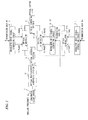
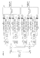
- FIG. 1 is a diagram showing a configuration of the optical modulation circuit of the present embodiment.
- the optical modulation circuit of the present embodiment includes: a continuous light source 1 for outputting continuous light with an angular frequency of ⁇ c with a constant power; an optical multicarrier generation portion 2 for generating n (n ⁇ 2) optical multicarriers from an optical carrier emitted from the continuous light source 1; an optical dividing portion 3 for dividing the optical multicarriers according to their wavelength; optical IQ-modulators 4-1 to 4-n for generating optical subcarriers in which phase-shift keying is superimposed on the respective divisions of the optical multicarrier; an optical combining portion 5 for combining the optical subcarriers that have been divided and modulated; and modulator drive signal generation circuits 6-1 to 6-n for generating a modulator drive signal from data.
- the present embodiment is characterized in that a multi-wavelength light source is used to generate an optical multicarrier.
- a bit rate and a band of a signal generated by a single optical IQ-modulator is made small. Consequently, it is possible to relax requirements such as an electric circuit speed of the modulator drive signal generation circuits 6-1 to 6-n and an operating band of the optical IQ-modulators 4-1 to 4-n.
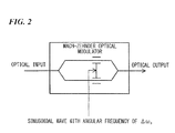
- a variable ⁇ s denotes a difference in angular frequency between the optical carrier and the optical multicarrier generated by a Mach-Zehnder optical modulator as shown in FIG. 2 .
- the Mach-Zehnder optical modulator is used to push-pull drive and modulate the light emitted from the continuous light source 1 at a minimum bias point by means of a clock signal which is a sinusoidal wave with an angular frequency of ⁇ s. Thereby, the optical carriers with an angular frequency of ⁇ c is suppressed. As a result, two optical multicarrier to which a double-sideband with carrier suppression modulation is imparted are generated as shown in Equation 1. This optical signal is put as s(t).
- s1 is input to the optical IQ-modulator 4-1
- s2 is input to the optical IQ-modulator 4-2.
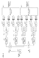
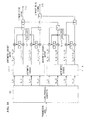
- the modulator drive signal generation circuit 6-1 has a configuration as shown in FIG. 3 . Allowing the data to be input as D1(t), D1(t) is divided into four pieces of parallel data: I1u(t), I1d(t), Q1u(t), and Q1d(t) by a serial/parallel converter 10.
- the divided signals are transformed into four outputs: I1u(t)+I1d(t), I1u(t)-I1d(t), Q1u(t)+Q1d(t), and, Q1d(t)-Q1u(t) by an arithmetic circuit 11. They are modulated pairwise by a sinusoidal wave with an angular frequency of ⁇ that has been emitted from an oscillator 12 and by a sinusoidal wave with a ⁇ /2 phase delay, respectively. The modulated outputs are added and output as ID1(t) and QD1(t), which are respectively expressed as Equation 4 and Equation 5.
- QD ⁇ 1 t I ⁇ 1 ⁇ u t + I ⁇ 1 ⁇ d t ⁇ cos ⁇ t + Q ⁇ 1 ⁇ u t + Q ⁇ 1 ⁇ d t ⁇ sin ⁇ t
- the output signal S1(t) is an optical subcarrier in which phase-shift keying is superimposed on angular frequencies of ⁇ from an angular frequency ⁇ c+ ⁇ s of the optical carrier of s1(t), which is expressed as Equation 6.
- ⁇ k denotes an angular frequency of the optical multicarrier that has been output from the multi-wavelength light source.
- An ⁇ k satisfies Equation 9, where 1, m (1, m ⁇ n) are variant integers.
- S1 to Sn that have been output respectively from the optical IQ-modulators 4-1 to 4-n are combined by the optical combining portion 5.
- the resultant signal is then output from the optical modulation circuit, with a spectrum as shown in FIG. 4B .
- the optical multicarrier generation portion 2 has a configuration in which, instead of a Mach-Zehnder modulator, a phase-shift modulator is driven with a sinusoidal wave with an angular frequency of ⁇ s, it is possible to generate three optical multicarriers: ⁇ c, ⁇ c+ ⁇ s, and ⁇ c- ⁇ s.
- the phase-shift modulator and the intensity modulator are serially connected and driven with synchronized clock signals, it is possible to generate n optical multicarriers.
- a second embodiment of the present invention will be described with reference to FIG. 5 to FIG. 8 .
- the description is for the case where the distance between the optical subcarriers is equal to the symbol rate of the optical subcarriers.
- FIG. 5 is a diagram showing a configuration of an optical transmission system of the present embodiment.
- the optical IQ-modulators 4-1 and 4-2, the optical multicarrier generation portion 2, and the modulator drive signal generation circuit 6-1 and 6-2 in the optical transmitter 20 of the present embodiment are configured similarly to those in the first embodiment, which are shown in FIG. 1 and FIG. 3 .
- this configuration it is possible to superimpose phase-shift keying on each optical subcarrier.
- quaternary differential phase-shift keying (DQPSK) is employed.
- the bit rate of the data #1 and the data #2 that are respectively input to the modulator drive signal generation circuits 6-1 and 6-2 is B (b/s). Therefore, data with 2B (b/s) in total is transmitted.
- the optical subcarrier signal that has been output from the optical transmitter 20 propagates through an optical transmission path 30 and is input to an optical receiver 40.
- signals parallelized from the data #1 by the serial/parallel converter 10 are denoted as I1u(t), I1d(t), Q1u(t), and Q1d(t).
- Signals parallelized from the data #2 by the serial/parallel converter 10 are denoted as I2u(t), I2d(t), Q2u(t), and Q2d(t).
- ⁇ s B/4 (Hz).
- the optical receiver 40 is made of: Mach-Zehnder interferometer filters (MZIs) 41-1 to 41-11 with a free spectral range (FSR) of one of B/2 (Hz), B (Hz), and B/4 (Hz); optical branching portions 42-1 to 42-4; and balanced O/E converters 43-1 to 43-8.
- An optical signal that has been input to the optical receiver 40 is fist divided into two pairs of subcarriers by the MZI 41-1 with an FSR of B/2, as shown in FIG. 7A and FIG. 7B.
- FIG. 7A shows a spectrum at point A in FIG. 6 .
- FIG. 7B shows a spectrum at point B in FIG. 6 .
- the optical signal is input to the MZIs 41-2 and 41-3 with an FSR of B (Hz), where the adjacent optical subcarriers are separated. Furthermore, each optical subcarrier is divided into two optical signals with a half power respectively by the optical branching portions 42-1 to 42-4. Each of the divided optical subcarriers is then input respectively to the MZIs 41-4 to 41-11 with an FSR of B/4 (Hz). Thereby, a 1-bit delay is imparted to each optical subcarrier.
- optical subcarriers are then converted into pieces of binary data I1u(t), I1d(t), Q1u(t), Q1d(t), I2u(t), I2d(t), Q2u(t), and Q2d(t) respectively by the balanced O/E converters 43-1 to 43-8.
- the pieces of binary data are demodulated into the original data #1 and the original data #2 by the parallel/serial converters 44-1 and 44-2.
- the present embodiment is characterized in that , because the distance between the optical subcarriers and the symbol rate of the optical subcarriers take the same orthogonal state, it is possible to separate and detect optical subcarriers without receiving linear interference and that the operating band of the necessary electrical/optical circuit are relaxed compared with those of single-carrier transmission.
- optical gate circuits 45-1 to 45-4 which have been driven with a sinusoidal wave with the same frequency as the symbol rate for a single optical subcarrier, are inserted directly before the optical couplers 42-1 to 42-4 respectively, it is possible to suppress interference, thus improving transmission quality.
- the optical subcarriers are received after they are mixed with local oscillator light (local light) with a frequency substantially equal to that of the optical subcarriers. Thereby, it is possible to demodulate the optical subcarriers.
- optical couplers 46-1 to 46-8 are provided instead of the MZIs 41-4 to 41-11 with a 1-bit delay, as shown in FIG. 8 .
- local oscillator light sources 47-1 to 47-4 and 90° phase shifters 48-1 to 48-4 two beams of local oscillator light whose phases are 90° different from each other are mixed with the two branched optical subcarriers, respectively. Thereby, it is possible to perform a heterodyne or homodyne detection on each channel by use of local oscillator light.
- An optical modulation circuit of a third embodiment of the present invention will be described with reference to FIG. 9 and FIG. 10 .
- the description has been for the case where a plurality of optical subcarriers on which differential phase-shift keying (DQPSK) is employed are generated.
- DQPSK differential phase-shift keying
- the third embodiment the case where phase-shift keying is superimposed on a plurality of optical subcarriers will be described.
- the optical modulation circuit of the third embodiment has a configuration that includes: a continuous light source 1 for outputting continuous light with a constant power; an optical IQ-modulator 4 for generating subcarriers on which phase-shift keying is employed; and a modulator drive signal generation circuit 6 for generating a modulator drive signal from data, as shown in FIG. 9 .
- a configuration of the modulator drive signal generation circuit 6 is shown in FIG. 10 .
- An optical carrier with an angular frequency of ⁇ c emitted from the continuous light source 1 is incident on the optical IQ-modulator 4, and is divided into two paths #1 and #2.
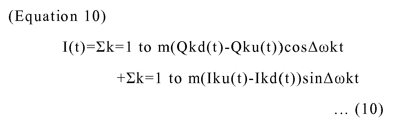
- a signal in the path #1 is modulated with a drive signal I(t) expressed by Equation 10.
- a signal in the path #2 is modulated with a drive signal Q(t) expressed by Equation 11.
- the drive signals I(t) and Q(t) are generated by the modulator drive signal generation circuit 6.
- the data superimposed on an upper sideband of the optical carrier is denoted by an adscript u.
- the data superimposed on a lower sideband of the optical carrier is denoted by an adscript d.
- 12u(t) denotes data of an in-phase component superimposed on the subcarrier with ⁇ +2 ⁇ .
- Iku and Qku may be in a signal constellation of quadrature amplitude modulation (QAM).
- the circuit configurations corresponding to the modulator drive signal generation circuits 6-1 and 6-2 are each replaced with the circuit configuration for generating a plurality of optical subcarriers, as shown in FIG. 10 , described in the third embodiment.
- the adjustment of the number of carriers generated by the optical multicarrier generation portion 2 and the optical IQ-modulators 4-1 and 4-2 it is possible to generate an optional number of optical subcarriers with the frequency of the optical carrier of the continuous light source 1 at their center.
- optical modulation circuit described in the fourth embodiment an optical receiver as shown in FIG. 6 made of Mach-Zehnder interferometer filters connected in multiple stages, optical couplers, and photoelectric converters is used. Thereby, it is possible to constitute an optical transmission system in which intensity modulation or phase-shift keying is superimposed on an optional number of optical subcarriers.
- an optical gate circuit that has been driven with a sinusoidal wave with the same frequency as the symbol rate for a single optical subcarrier may be inserted directly before each optical branching portion.
- the present invention it is possible to implement multicarrier transmission capable reducing the number of oscillators and the operating frequency of the electrical/optical circuit that are required in generation of optical subcarriers to half or less those of the conventional one, capable of narrowing an occupied band, and capable of suppressing a chromatic dispersion and a PMD, and an influence of a nonlinear optical effect. Therefore, it is possible to reduce the amount of hardware when an optical transmission system is constructed, and also to improve communication quality.
Landscapes
- Physics & Mathematics (AREA)
- Engineering & Computer Science (AREA)
- Nonlinear Science (AREA)
- Computer Networks & Wireless Communication (AREA)
- Optics & Photonics (AREA)
- Electromagnetism (AREA)
- Signal Processing (AREA)
- General Physics & Mathematics (AREA)
- Chemical & Material Sciences (AREA)
- Ceramic Engineering (AREA)
- Crystallography & Structural Chemistry (AREA)
- Optical Communication System (AREA)
- Optical Modulation, Optical Deflection, Nonlinear Optics, Optical Demodulation, Optical Logic Elements (AREA)
Abstract
Description
- The present invention relates to a multicarrier modulation technique for transmitting binary data in a plurality of subcarriers.
Priority is claimed on Japanese Patent Application No.2007-177871, filed on July 6, 2007 - As a technique for providing a large capacity in optical fiber transmission, the wavelength division multiplexing (WDM) technique is used in which a symbol rate for a single carrier is increased to narrow the channel spacing for an increased number of multiplexes, to thereby achieve an enlarged transmission capacity.
- However, an increase in symbol rate results in a more noticeable influence of a chromatic dispersion and a polarization mode dispersion (PMD) in a transmission fiber. Therefore, a sophisticated compensation technique is required. In addition, in order to obtain necessary receiver sensitivity, more power is required. This leads to a problem of suppressing a nonlinear optical effect produced in the fiber such as self phase modulation (SPM), four wave mixing (FWM), or cross phase modulation (XPM). In addition, with the increase in symbol rate, an occupied band for a single channel is expanded. This makes it difficult to increase the number of WDM channels.
- Here, symbol rate is synonymous with baud rate, which is a bit rate to be transmitted divided by the number of bits of the modulation code. For example, if it is assumed that the bit rate is B (b/s) and that an M-ary modulation code is used, then the symbol rate is given by B/log2 (M) (symbol/sec).
- To solve this problem, what used to be transmitted in a single carrier manner is divided into subcarriers at a symbol rate that does not require a sophisticated compensation technique and then the subcarriers are transmitted. Thereby, it is possible to suppress chromatic dispersion and PMD, and an influence of a nonlinear optical effect.
- If an orthogonal frequency division multiplexing (OFDM) modulation, which is often used in wireless transmission, is performed on data, and continuous light emitted from a continuous light source is modulated by an intensity modulator or a single sideband (SSB) modulator driven with an OFDM signal, then optical OFDM transmission can be implemented (for example, see
Patent Document 1, or Non-PatentDocument 1 or 2). -
- Patent Document 1: Japanese Unexamined Patent Application, First Publication No.
2005-311722 - Non-Patent Document 1: Arthur James Lowery et al., "Orthogonal Frequency Division Multiplexing for Adaptive Dispersion Compensation in Long Haul WDM Systems," Optical Fiber Communication Conference 2006, PDP39 (2006)
- Non-Patent Document 2: Brendon J. C. Schmidt et al., "Experimental Demonstration of 20 Gbit/s Direct-Detection Optical OFDM and 12 Gbit/s with a colorless transmitter," Optical Fiber Communication Conference 2007, PDP18 (2007).
- However, the scheme using an intensity modulator or an SSB modulator has the following problems.
To generate an OFDM signal from a data signal as described inNon-Patent Documents Patent Document 1, there are required as many modulators as the optical subcarriers that are intended to be generated, and an oscillator that supplies a clock with a frequency equal to the symbol rate of the data signal to a modulator drive signal generation circuit. Therefore, it is difficult to obtain a high-speed operation and control. - Patterns of optical modulation will be described with reference to
FIG. 11A to FIG. 11C . InFIG. 11A to FIG. 11C , the axis of abscissa represents optical frequency, and the axis of ordinate represents optical intensity.FIG. 11A and FIG. 11B show an optical spectrum in conventional modulation schemes. In the case where an intensity modulator is driven with an OFDM signal, the optical spectrum is as shown inFIG. 11A . The identical subcarrier groups are produced on both sides of the optical carrier frequency. This results in a problem in that the occupied band is wider than in the single carrier transmission. - Furthermore, in the case where an intensity modulator and an SSB modulator are driven with an OFDM signal, the optical spectrum is as shown respectively in
FIG. 11A and FIG. 11B . Therefore, to efficiently wavelength-multiplex the optical OFDM signal, it is required to use an optical filter to filter an optical carrier with a frequency of fc emitted from the continuous light source, to thereby cut out an optical OFDM signal. Alternatively, it is required to perform an SSB modulation on the optical carrier. In addition, in the case where an OFDM signal in a single sideband is suppressed by filtering, it is required to insert a guard band. This makes requirements for the electrical/optical circuit more rigid. - In the case of wavelength-multiplexing an optical OFDM signal that is produced by modifying continuous light emitted from a continuous light source by means of an intensity modulator or an SSB modulator driven with an OFDM signal, the aforementioned problems arise. Therefore, it is required to provide a guard band. This prevents effective utilization of frequency bands of light.
- The present invention has been achieved against such a backdrop, and has an object to provide an optical modulation circuit and an optical transmission system capable of reducing the number of oscillators and the drive frequency that are required in generation of optical subcarriers to half or less those of the conventional one, capable of narrowing an occupied band (for example, see
FIG. 11C ), and capable of suppressing chromatic dispersion and PMD, and an influence of a nonlinear optical effect, in optical transmission. - An optical modulation circuit of the present invention comprises: a continuous light source which generates continuous light with a constant power; a modulator drive signal generation unit which modulates data to be transmitted into modulator drive signals such as to generate optical subcarriers which have m (m≥1) and 1 (1≥1) (in total, 1+m) different frequencies respectively before and after a frequency of the continuous light and on which different data is superimposed; and an optical modulation unit which modulates the continuous light from the continuous light source into the optical subcarriers using the modulator drive signals.
In the optical modulation circuit of the present invention, the modulator drive signal generation unit may generate the modulator drive signal which superimposes phase-shift keying, intensity modulation, and quadrature amplitude modulation for every frequency of the optical subcarriers. - The optical modulation circuit of the present invention may comprise: an optical multicarrier generation unit which generates optical multicarriers with co-phased n (n≥2) different frequencies based on the continuous light from the continuous light source; an optical dividing unit which divides the optical multicarrier for each of the n different frequencies so as to output n optical carriers; and an optical combining unit connected to the optical modulation unit, wherein the modulator drive signal generation unit modulates data to be transmitted into n of the modulator drive signals such as to generate optical subcarriers which further have the m (m≥1) and 1 (1≥1) (in total, 1+m) different frequencies respectively before and after each of the frequencies of the n optical carriers and on which different data is superimposed, the modulation unit uses the n modulator drive signals to further modulate the n optical carriers into 1+m of the optical subcarriers, and the optical combining unit combines a total of n×(1+m) of the optical subcarriers.
In this manner, the optical multicarrier generation portion is used to generate optical multicarriers. Thereby, it is possible to decrease the bit rate and the band of the signal generated by every optical modulator compared with the case where the same number of optical subcarriers at the same transmission speed is generated without using the optical multicarrier generation portion. Therefore, it is possible to mitigate requirements such as an electric circuit speed of the modulator drive signal generation portion and an operating band of the optical modulators. - The optical modulation circuit of the present invention may make the symbol rate of the optical subcarriers equal to the distance between the optical subcarriers, to thereby put the optical subcarriers and the distance between the optical subcarriers in an orthogonal state. Consequently, it is possible to detect the optical subcarriers without receiving linear interference and also to narrow the necessary band of light compared with that in a single carrier transmission.
- In the optical modulation circuit of the present invention, the multicarrier generation unit may impart a double-sideband with carrier suppression modulation by a sinusoidal wave to the continuous light source.
- In the optical modulation circuit of the present invention, the optical modulation unit may comprise n optical IQ-modulators.
- In the optical modulation circuit of the present invention, the modulator drive signal generation unit may convert transmission data into two pieces of parallel data: A(t) and B(t), may generate an I-phase signal resulting from A(t)+B(t) modified with a clock signal with an angular frequency of ω and a Q-phase signal resulting from A(t)-B(t) modified with a signal that is out of phase by π/2 from the clock signal, and may apply the I-phase signal and the Q-phase signal on corresponding electrodes of each of the optical IQ-modulators.
- In the optical modulation circuit of the present invention, the modulator drive signal generation unit may convert transmission data into 2n pieces of parallel data of A1(t), A2(t), ..., An(t) and B1(t), B2(t), ..., Bn(t), may generate an I-phase signal resulting from adding the 2n pieces of parallel data for k=1 to n, which have been modified respectively with n clock signals with angular frequencies of ω1, ω2, ..., ωn and a Q-phase signal resulting from adding Ak(t)-Bk(t) for k=1, 2, ..., n, each of which has been modified respectively with a signal that is out of phase by π/2 from a clock signal with an angular frequency of ωk for k=1 to n, and may apply the I-phase signal and the Q-phase signal on corresponding electrodes of each of the IQ-modulators.
- In the optical modulation circuit of the present invention, the modulator drive signal generation unit may convert transmission data into four pieces of parallel data: I1(t), I2(t), Q1(t), and Q2(t), may generate: an I-phase signal in which a signal resulting from Q2(t)-Q1(t) modified with a clock signal with an angular frequency of ω is added to a signal resulting from I1(t)-I2(t) modified with a signal that is out of phase by π/2 from the clock signal; and a Q-phase signal in which a signal resulting from I1(t)+I2(t) modified with a clock signal with an angular frequency of ω is added to a signal resulting from Q2(t)+Q1(t) modified with a signal that is out of phase by π/2 from the clock signal, and may apply the I-phase signal and the Q-phase signal on corresponding electrodes of each of the IQ-modulators.
- Furthermore, another aspect of the present invention can be an optical transmission system comprising: an optical transmitter comprising an optical modulation circuit of the present invention; an optical transmission path which transmits an optical subcarrier emitted from the optical transmitter; and an optical receiver which converts the optical subcarrier having been transmitted over the optical transmission path into an electrical signal.
- At this time, the optical receiver may comprise Mach-Zehnder interferometer filters connected in multiple stages, optical couplers, and photoelectric converters. Alternatively, the optical receiver may comprise the Mach-Zehnder interferometer (MZI) filters connected in multiple stages, the optical couplers, optical gate circuits, and the photoelectric converters.
- Furthermore, seeing the present invention from an aspect of an optical modulation method, the present invention is an optical modulation method in which an optical modulation circuit: generates continuous light with a constant power from a continuous light source; modulates data to be transmitted into modulator drive signals such as to generate optical subcarriers which have m (m≥1) and 1 (1≥1) (in total, 1+m) different frequencies respectively before and after a frequency of the continuous light and on which different data is superimposed, by a modulator drive signal generation unit; and modulates the continuous light from the continuous light source into the optical subcarriers using the modulator drive signals, by an optical modulation unit.
- According to the present invention, it is possible to implement multicarrier transmission capable of reducing the number of oscillators and the drive frequency that are required in generation of optical subcarriers to half or less those of the conventional one, capable of narrowing an occupied band, and capable of suppressing a chromatic dispersion and a PMD, and an influence of a nonlinear optical effect.
-
- [
Fig. 1 ]
FIG. 1 is a configuration diagram showing an optical modulation circuit of a first embodiment. - [
Fig. 2 ]
FIG. 2 is a configuration diagram showing an optical multicarrier generation portion of the first embodiment. - [
Fig. 3 ]
FIG. 3 is a configuration diagram showing a modulator drive signal generation circuit of the first embodiment. - [
Fig. 4A ]
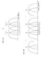
FIG. 4A is a diagram showing an output spectrum of the optical modulation circuit of the first embodiment. - [
Fig. 4B ]
FIG. 4B is a diagram showing an output spectrum of the optical modulation circuit of the first embodiment. - [
Fig. 5 ]
FIG. 5 is a configuration diagram showing an optical transmission system of a second embodiment. - [
Fig. 6 ]
FIG. 6 is a configuration diagram showing an optical receiver of the second embodiment. - [
Fig. 7A ]
FIG. 7A is a diagram showing a spectrum of an optical signal after passing through an MZI of the second embodiment. - [
Fig. 7B ]
FIG. 7B is a diagram showing a spectrum of an optical signal after passing through the MZI of the second embodiment. - [
Fig. 8 ]
FIG. 8 is a configuration diagram showing an optical receiver applied to a QPSK of the second embodiment. - [
Fig. 9 ]
FIG. 9 is a configuration diagram showing an optical modulation circuit of a third embodiment. - [
Fig. 10 ]
FIG. 10 is a configuration diagram showing an optical modulation circuit drive signal generation portion of the third embodiment. - [
Fig. 11A ]
FIG. 11A is a diagram showing an optical spectrum in a conventional modulation scheme. - [
Fig. 11B ]
FIG. 11B is a diagram showing an optical spectrum in a conventional modulation scheme - [
Fig. 11C ]
FIG. 11C is a diagram showing an optical spectrum in an optical modulation circuit of the present invention. -
- 1
- continuous light source
- 2
- optical multicarrier generation portion
- 3
- optical dividing portion
- 4, 4-1 to 4-n
- optical IQ-modulator
- 5
- optical combining portion
- 6, 6-1 to 6-n
- modulator drive signal generation circuit
- 10
- serial/parallel converter
- 11, 11-1 to 11-n
- arithmetic circuit
- 12, 12-1 to 12-n
- oscillator
- 20
- optical transmitter
- 30
- optical transmission path
- 40
- optical receiver
- 41-1 to 41-11
- Mach-Zehnder interferometer filter
- 42-1 to 42-4
- optical coupler
- 43-1 to 43-8
- balanced O/E converter
- 44-1, 44-2
- parallel/serial converter
- 45-1 to 45-4
- optical gate circuit
- 46-1 to 46-8
- optical coupler
- 47-1 to 47-4
- local oscillator light source
- 48-1 to 48-4
- 90° phase shifter
- An optical modulation circuit using a multi-wavelength light source as a first embodiment of the present invention will be described with reference to
FIG. 1 to FIG. 4B . - In the present embodiment, the multi-wavelength light source is made of a continuous
light source 1 and an opticalmulticarrier generation portion 2. -
FIG. 1 is a diagram showing a configuration of the optical modulation circuit of the present embodiment. As shown inFIG. 1 , the optical modulation circuit of the present embodiment includes: a continuouslight source 1 for outputting continuous light with an angular frequency of ωc with a constant power; an opticalmulticarrier generation portion 2 for generating n (n≥2) optical multicarriers from an optical carrier emitted from the continuouslight source 1; anoptical dividing portion 3 for dividing the optical multicarriers according to their wavelength; optical IQ-modulators 4-1 to 4-n for generating optical subcarriers in which phase-shift keying is superimposed on the respective divisions of the optical multicarrier; an optical combiningportion 5 for combining the optical subcarriers that have been divided and modulated; and modulator drive signal generation circuits 6-1 to 6-n for generating a modulator drive signal from data. - Here, the present embodiment is characterized in that a multi-wavelength light source is used to generate an optical multicarrier. Thereby, compared with the case of generating the same number of optical subcarriers with the same bit-rate without using a multi-wavelength light source, a bit rate and a band of a signal generated by a single optical IQ-modulator is made small. Consequently, it is possible to relax requirements such as an electric circuit speed of the modulator drive signal generation circuits 6-1 to 6-n and an operating band of the optical IQ-modulators 4-1 to 4-n.
- Next is a description of an operation of the first embodiment. For convenience' sake, the description is for the case where the number of optical multicarriers emitted from the multi-wavelength light source is n=2 and the number of optical subcarriers generated by the optical IQ-modulator is 1+m=2, that is, for the case where the total number of optical subcarriers generated is n×(1+m)=4, by way of example.
It is assumed that each bit rate ofdata # 1 anddata # 2 to be transmitted is B (b/s). A variable ωc denotes an angular frequency of the optical carrier emitted from the continuouslight source 1. A variable Δωs denotes a difference in angular frequency between the optical carrier and the optical multicarrier generated by a Mach-Zehnder optical modulator as shown inFIG. 2 . The following description is for the case where the frequency spacing between the optical subcarriers is equal to the symbol rate of the optical subcarriers. At this time, the relation Δωs=2Δω is satisfied. - The Mach-Zehnder optical modulator is used to push-pull drive and modulate the light emitted from the continuous
light source 1 at a minimum bias point by means of a clock signal which is a sinusoidal wave with an angular frequency of Δωs. Thereby, the optical carriers with an angular frequency of ωc is suppressed. As a result, two optical multicarrier to which a double-sideband with carrier suppression modulation is imparted are generated as shown inEquation 1. This optical signal is put as s(t).
The optical signal s(t) is divided into
and
by theoptical dividing portion 3. Here, s1 is input to the optical IQ-modulator 4-1, and s2 is input to the optical IQ-modulator 4-2. - Next is a description of an operation of the optical IQ-modulator 4-1. The modulator drive signal generation circuit 6-1 has a configuration as shown in
FIG. 3 . Allowing the data to be input as D1(t), D1(t) is divided into four pieces of parallel data: I1u(t), I1d(t), Q1u(t), and Q1d(t) by a serial/parallel converter 10. - The divided signals are transformed into four outputs: I1u(t)+I1d(t), I1u(t)-I1d(t), Q1u(t)+Q1d(t), and, Q1d(t)-Q1u(t) by an
arithmetic circuit 11. They are modulated pairwise by a sinusoidal wave with an angular frequency of Δω that has been emitted from anoscillator 12 and by a sinusoidal wave with a π/2 phase delay, respectively. The modulated outputs are added and output as ID1(t) and QD1(t), which are respectively expressed asEquation 4 andEquation 5. -


When the optical IQ-modulator 4-1 is driven with these signals, an optical signal that is output from the optical IQ-modulator 4-1 is generated as an output signal S1(t). The output signal S1(t) is an optical subcarrier in which phase-shift keying is superimposed on angular frequencies of ±Δω from an angular frequency ωc+Δωs of the optical carrier of s1(t), which is expressed asEquation 6. -

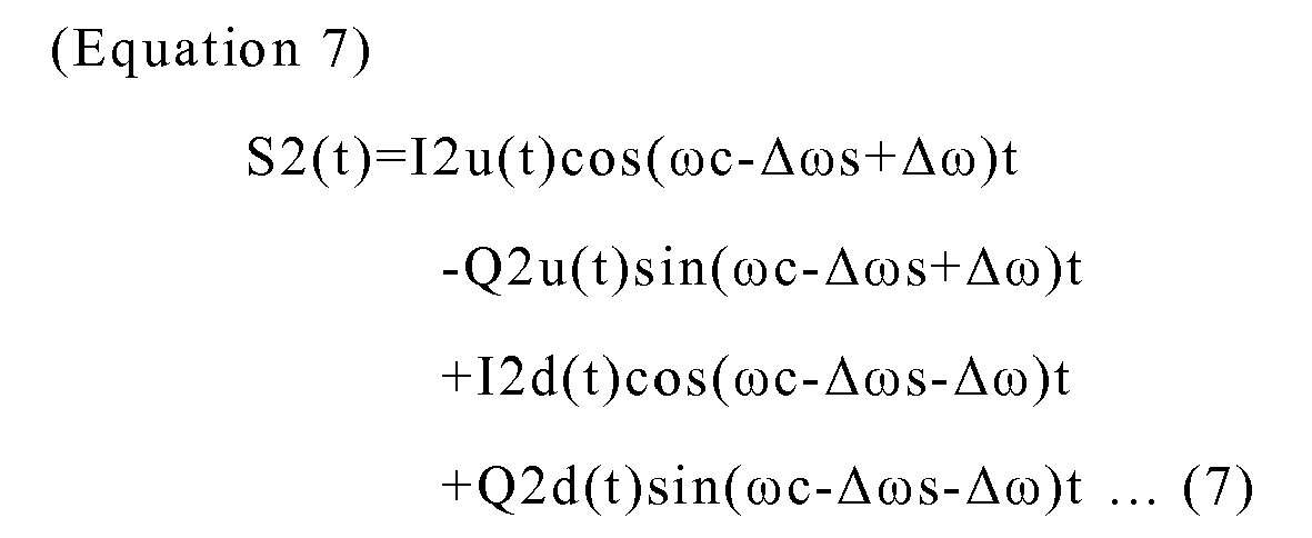
- Similarly, an output signal S2(t) of the optical IQ-modulator 4-2 is expressed as Equation 7.
- S1 and S2 that have been output respectively from the optical IQ-modulators 4-1 and 4-2 are combined by the optical combining
portion 5. The resultant signal is then output from the optical modulation circuit, with a spectrum as shown inFIG. 4A . As shown inFIG. 4A , according to the present invention, the signal band is narrowed more than in single carrier transmission, and also the symbol rate for a single subcarrier is lowered. Therefore, chromatic dispersion and PMD tolerances improve. Furthermore, precoding the input date makes it possible to superimpose a differential phase-shift keying code.
For convenience' sake, the description above has been for the case where the number of optical multicarriers emitted from the multi-wavelength light source is two, by way of example. However, in the more general case where the number of optical multicarrier is n, the output signal is expressed asEquation 8.
where ωk denotes an angular frequency of the optical multicarrier that has been output from the multi-wavelength light source. An ωk satisfies Equation 9, where 1, m (1, m≤n) are variant integers.
In this case, S1 to Sn that have been output respectively from the optical IQ-modulators 4-1 to 4-n are combined by the optical combiningportion 5. The resultant signal is then output from the optical modulation circuit, with a spectrum as shown inFIG. 4B . - Furthermore, if the optical
multicarrier generation portion 2 has a configuration in which, instead of a Mach-Zehnder modulator, a phase-shift modulator is driven with a sinusoidal wave with an angular frequency of Δωs, it is possible to generate three optical multicarriers: ωc, ωc+Δωs, and ωc-Δωs. In addition, if the phase-shift modulator and the intensity modulator are serially connected and driven with synchronized clock signals, it is possible to generate n optical multicarriers. - A second embodiment of the present invention will be described with reference to
FIG. 5 to FIG. 8 . In the present embodiment, the description is for the case where the distance between the optical subcarriers is equal to the symbol rate of the optical subcarriers. -
FIG. 5 is a diagram showing a configuration of an optical transmission system of the present embodiment. The optical IQ-modulators 4-1 and 4-2, the opticalmulticarrier generation portion 2, and the modulator drive signal generation circuit 6-1 and 6-2 in theoptical transmitter 20 of the present embodiment are configured similarly to those in the first embodiment, which are shown inFIG. 1 andFIG. 3 . In this configuration, it is possible to superimpose phase-shift keying on each optical subcarrier. In the present embodiment, quaternary differential phase-shift keying (DQPSK) is employed. - It is assumed that the bit rate of the
data # 1 and thedata # 2 that are respectively input to the modulator drive signal generation circuits 6-1 and 6-2 is B (b/s). Therefore, data with 2B (b/s) in total is transmitted. The optical subcarrier signal that has been output from theoptical transmitter 20 propagates through anoptical transmission path 30 and is input to anoptical receiver 40. - Similarly to the first embodiment, signals parallelized from the
data # 1 by the serial/parallel converter 10 are denoted as I1u(t), I1d(t), Q1u(t), and Q1d(t). Signals parallelized from thedata # 2 by the serial/parallel converter 10 are denoted as I2u(t), I2d(t), Q2u(t), and Q2d(t). In the present embodiment, Δωs=B/4 (Hz). - As shown in
FIG. 6 , theoptical receiver 40 is made of: Mach-Zehnder interferometer filters (MZIs) 41-1 to 41-11 with a free spectral range (FSR) of one of B/2 (Hz), B (Hz), and B/4 (Hz); optical branching portions 42-1 to 42-4; and balanced O/E converters 43-1 to 43-8. An optical signal that has been input to theoptical receiver 40 is fist divided into two pairs of subcarriers by the MZI 41-1 with an FSR of B/2, as shown inFIG. 7A and FIG. 7B. FIG. 7A shows a spectrum at point A inFIG. 6 .FIG. 7B shows a spectrum at point B inFIG. 6 . - Next, the optical signal is input to the MZIs 41-2 and 41-3 with an FSR of B (Hz), where the adjacent optical subcarriers are separated. Furthermore, each optical subcarrier is divided into two optical signals with a half power respectively by the optical branching portions 42-1 to 42-4. Each of the divided optical subcarriers is then input respectively to the MZIs 41-4 to 41-11 with an FSR of B/4 (Hz). Thereby, a 1-bit delay is imparted to each optical subcarrier. The optical subcarriers are then converted into pieces of binary data I1u(t), I1d(t), Q1u(t), Q1d(t), I2u(t), I2d(t), Q2u(t), and Q2d(t) respectively by the balanced O/E converters 43-1 to 43-8.
- The pieces of binary data are demodulated into the
original data # 1 and theoriginal data # 2 by the parallel/serial converters 44-1 and 44-2. - Here, the present embodiment is characterized in that, because the distance between the optical subcarriers and the symbol rate of the optical subcarriers take the same orthogonal state, it is possible to separate and detect optical subcarriers without receiving linear interference and that the operating band of the necessary electrical/optical circuit are relaxed compared with those of single-carrier transmission.
- Furthermore, if optical gate circuits 45-1 to 45-4, which have been driven with a sinusoidal wave with the same frequency as the symbol rate for a single optical subcarrier, are inserted directly before the optical couplers 42-1 to 42-4 respectively, it is possible to suppress interference, thus improving transmission quality.
- In the case where QPSK is superimposed on each optical subcarrier instead of DQPSK, it is not possible to perform a differential detection. Therefore, instead of performing a differential detection by use of the MZIs 41-4 to 41-11 with a 1-bit delay, the optical subcarriers are received after they are mixed with local oscillator light (local light) with a frequency substantially equal to that of the optical subcarriers. Thereby, it is possible to demodulate the optical subcarriers.
- As for a specific configuration therefor, optical couplers 46-1 to 46-8 are provided instead of the MZIs 41-4 to 41-11 with a 1-bit delay, as shown in
FIG. 8 . By use of local oscillator light sources 47-1 to 47-4 and 90° phase shifters 48-1 to 48-4, two beams of local oscillator light whose phases are 90° different from each other are mixed with the two branched optical subcarriers, respectively. Thereby, it is possible to perform a heterodyne or homodyne detection on each channel by use of local oscillator light. - An optical modulation circuit of a third embodiment of the present invention will be described with reference to
FIG. 9 andFIG. 10 . In the second embodiment, the description has been for the case where a plurality of optical subcarriers on which differential phase-shift keying (DQPSK) is employed are generated. However, in the third embodiment, the case where phase-shift keying is superimposed on a plurality of optical subcarriers will be described. - The optical modulation circuit of the third embodiment has a configuration that includes: a continuous
light source 1 for outputting continuous light with a constant power; an optical IQ-modulator 4 for generating subcarriers on which phase-shift keying is employed; and a modulator drivesignal generation circuit 6 for generating a modulator drive signal from data, as shown inFIG. 9 . A configuration of the modulator drivesignal generation circuit 6 is shown inFIG. 10 . - An optical carrier with an angular frequency of ωc emitted from the continuous
light source 1 is incident on the optical IQ-modulator 4, and is divided into twopaths # 1 and #2. A signal in thepath # 1 is modulated with a drive signal I(t) expressed byEquation 10. A signal in thepath # 2 is modulated with a drive signal Q(t) expressed byEquation 11. The drive signals I(t) and Q(t) are generated by the modulator drivesignal generation circuit 6. - Here, the data superimposed on an upper sideband of the optical carrier is denoted by an adscript u. The data superimposed on a lower sideband of the optical carrier is denoted by an adscript d. For example, 12u(t) denotes data of an in-phase component superimposed on the subcarrier with ω+2Δω.
-

Furthermore, to the signal in thepath # 2 is imparted a π/2 phase delay with respect to the optical carrier. Therefore, the combination of the optical signals in the two paths yields an output signal Sout(t) expressed byEquation 12.
As described above, 2m optical subcarriers on which phase-shift keying is superimposed are generated with the angular frequency ωc of the optical carrier emitted from the continuouslight source 1 at their center. According to the present invention, the signal band is more narrowed than in single carrier transmission. In addition, the symbol rate for a single subcarrier is lowered. Therefore, chromatic dispersion and PMD tolerances improve. Furthermore, in the present embodiment, Iku and Qku may be in a signal constellation of quadrature amplitude modulation (QAM). - In the same configuration as that of the optical modulation circuit, as shown in
FIG. 1 , described in the first embodiment, the circuit configurations corresponding to the modulator drive signal generation circuits 6-1 and 6-2 are each replaced with the circuit configuration for generating a plurality of optical subcarriers, as shown inFIG. 10 , described in the third embodiment. With the adjustment of the number of carriers generated by the opticalmulticarrier generation portion 2 and the optical IQ-modulators 4-1 and 4-2, it is possible to generate an optional number of optical subcarriers with the frequency of the optical carrier of the continuouslight source 1 at their center. - With the optical modulation circuit described in the fourth embodiment, an optical receiver as shown in
FIG. 6 made of Mach-Zehnder interferometer filters connected in multiple stages, optical couplers, and photoelectric converters is used. Thereby, it is possible to constitute an optical transmission system in which intensity modulation or phase-shift keying is superimposed on an optional number of optical subcarriers. - Furthermore, an optical gate circuit that has been driven with a sinusoidal wave with the same frequency as the symbol rate for a single optical subcarrier may be inserted directly before each optical branching portion.
- According to the present invention, it is possible to implement multicarrier transmission capable reducing the number of oscillators and the operating frequency of the electrical/optical circuit that are required in generation of optical subcarriers to half or less those of the conventional one, capable of narrowing an occupied band, and capable of suppressing a chromatic dispersion and a PMD, and an influence of a nonlinear optical effect. Therefore, it is possible to reduce the amount of hardware when an optical transmission system is constructed, and also to improve communication quality.
Claims (13)
- An optical modulation circuit comprising:a continuous light source which generates continuous light with a constant power;a modulator drive signal generation unit which modulates data to be transmitted into modulator drive signals such as to generate optical subcarriers which have m (m≥1) and 1 (1≥1) (in total, 1+m) different frequencies respectively before and after a frequency of the continuous light and on which different data is superimposed; andan optical modulation unit which modulates the continuous light from the continuous light source into the optical subcarriers using the modulator drive signals.
- The optical modulation circuit of claim 1, comprising:an optical multicarrier generation unit which generates optical multicarriers with n (n≥2) different frequencies based on the continuous light from the continuous light source;an optical dividing unit which divides the optical multicarrier for each of the n different frequencies so as to output n optical carriers; andan optical combining unit connected to the optical modulation unit,wherein the modulator drive signal generation unit modulates data to be transmitted into n of the modulator drive signals such as to generate optical subcarriers which further have the m (m≥1) and 1 (1≥1) (in total, 1+m) different frequencies respectively before and after each of the frequencies of the n optical carriers and on which different data is superimposed,the modulation unit uses the n modulator drive signals to further modulate the n optical carriers into 1+m of the optical subcarriers, andthe optical combining unit combines a total of n×(1+m) of the optical subcarriers.
- The optical modulation circuit of claim 2, wherein the optical modulation unit comprises n optical IQ-modulators.
- The optical modulation circuit of claim 3, wherein the modulator drive signal generation unit converts transmission data into two pieces of parallel data: A(t) and B(t),
generates an I-phase signal resulting from A(t)+B(t) modified with a clock signal with an angular frequency of ω and a Q-phase signal resulting from A(t)-B(t) modified with a signal that is out of phase by π/2 from the clock signal, and
applies the I-phase signal and the Q-phase signal on corresponding electrodes of each of the optical IQ-modulators. - The optical modulation circuit of claim 3, wherein the modulator drive signal generation unit converts transmission data into 2n pieces of parallel data of A1(t), A2(t), ..., An(t) and B1(t), B2(t), ..., Bn(t),
generates an I-phase signal resulting from adding the 2n pieces of parallel data for k=1 to n, which have been modified respectively with n clock signals with angular frequencies of ω1, ω2, ..., ωn and a Q-phase signal resulting from adding Ak(t)-Bk(t) for k=1, 2, ..., n, each of which has been modified respectively with a signal that is out of phase by π/2 from a clock signal with an angular frequency of ωk for k=1 to n, and
applies the I-phase signal and the Q-phase signal on corresponding electrodes of each of the IQ-modulators. - The optical modulation circuit of claim 3, wherein the modulator drive signal generation unit converts transmission data into four pieces of parallel data: I1(t), I2(t), Q1(t), and Q2(t),
generates: an I-phase signal in which a signal resulting from Q2(t)-Q1(t) modified with a clock signal with an angular frequency of ω is added to a signal resulting from I1(t)-I2(t) modified with a signal that is out of phase by π/2 from the clock signal; and a Q-phase signal in which a signal resulting from I1(t)+I2(t) modified with a clock signal with an angular frequency of ω is added to a signal resulting from Q2(t)+Q1(t) modified with a signal that is out of phase by ω/2 from the clock signal, and
applies the I-phase signal and the Q-phase signal on corresponding electrodes of each of the IQ-modulators. - The optical modulation circuit of one of claims 2 to 6, wherein the optical multicarrier generation unit imparts a double-sideband with carrier suppression modulation by a sinusoidal wave to the continuous light source.
- The optical modulation circuit of one of claims 1 to 7, wherein the modulator drive signal generation unit generates the modulator drive signal which superimposes phase-shift keying, intensity modulation, and quadrature amplitude modulation for every frequency of the optical subcarriers.
- The optical modulation circuit of one of claims 1 to 8, wherein the symbol rate of the optical subcarriers equals to the distance between the optical subcarriers.
- An optical transmission system comprising:an optical transmitter comprising an optical modulation circuit of one of claims 1 to 9;an optical transmission path which transmits an optical subcarrier emitted from the optical transmitter; andan optical receiver which converts the optical subcarrier having been transmitted over the optical transmission path into an electrical signal.
- The optical transmission system of claim 10, wherein the optical receiver comprises Mach-Zehnder interferometer filters connected in multiple stages, optical couplers, and photoelectric converters.
- The optical transmission system of claim 11, wherein the optical receiver comprises the Mach-Zehnder interferometer filters connected in multiple stages, the optical couplers, optical gate circuits, and the photoelectric converters.
- An optical modulation method in which an optical modulation circuit:generates continuous light with a constant power from a continuous light source;modulates data to be transmitted into modulator drive signals such as to generate optical subcarriers which have m (m≥1) and 1 (1≥1) (in total, 1+m) different frequencies respectively before and after a frequency of the continuous light and on which different data is superimposed, by a modulator drive signal generation unit; andmodulates the continuous light from the continuous light source into the optical subcarriers using the modulator drive signals, by an optical modulation unit.
Applications Claiming Priority (2)
| Application Number | Priority Date | Filing Date | Title |
|---|---|---|---|
| JP2007177871A JP4906103B2 (en) | 2007-07-06 | 2007-07-06 | Optical modulation circuit and optical transmission system |
| PCT/JP2008/062182 WO2009008370A1 (en) | 2007-07-06 | 2008-07-04 | Optical modulation circuit and optical transmission system |
Publications (3)
| Publication Number | Publication Date |
|---|---|
| EP2166681A1 true EP2166681A1 (en) | 2010-03-24 |
| EP2166681A4 EP2166681A4 (en) | 2014-01-01 |
| EP2166681B1 EP2166681B1 (en) | 2019-09-18 |
Family
ID=40228542
Family Applications (1)
| Application Number | Title | Priority Date | Filing Date |
|---|---|---|---|
| EP08777897.3A Active EP2166681B1 (en) | 2007-07-06 | 2008-07-04 | Optical modulation circuit and optical transmission system |
Country Status (5)
| Country | Link |
|---|---|
| US (1) | US8437638B2 (en) |
| EP (1) | EP2166681B1 (en) |
| JP (1) | JP4906103B2 (en) |
| CN (1) | CN101682422B (en) |
| WO (1) | WO2009008370A1 (en) |
Cited By (2)
| Publication number | Priority date | Publication date | Assignee | Title |
|---|---|---|---|---|
| WO2011032531A1 (en) * | 2009-09-18 | 2011-03-24 | Karlsruher Institut für Technologie | Optical arrangement |
| EP2403163A1 (en) * | 2010-06-29 | 2012-01-04 | France Telecom | Method and system for generation of QAM formats for applications in optical communication |
Families Citing this family (41)
| Publication number | Priority date | Publication date | Assignee | Title |
|---|---|---|---|---|
| JP4905951B2 (en) * | 2006-11-28 | 2012-03-28 | 日本電信電話株式会社 | Optical modulation circuit and optical transmission system |
| JP4941340B2 (en) * | 2008-02-04 | 2012-05-30 | Kddi株式会社 | Optical communication method and apparatus |
| TWI396033B (en) * | 2008-11-07 | 2013-05-11 | Univ Nat Chiao Tung | Multi - frequency electrical signal of the photoelectric device |
| EP2380291A1 (en) * | 2008-12-16 | 2011-10-26 | Alcatel-Lucent USA Inc. | Communication system and method with signal constellation |
| JP5411538B2 (en) * | 2009-03-16 | 2014-02-12 | 日本電信電話株式会社 | Optical multicarrier generation apparatus and method, and optical multicarrier transmission apparatus using optical multicarrier generation apparatus |
| JP5303323B2 (en) * | 2009-03-16 | 2013-10-02 | 日本電信電話株式会社 | Variable optical multicarrier generation apparatus, variable optical multicarrier transmission apparatus, and variable multicarrier generation method |
| CN101557270B (en) * | 2009-04-30 | 2012-08-15 | 华中科技大学 | Full-optical Fourier converter, inverse converter and orthogonal frequency division multiplexing system |
| US8929750B2 (en) * | 2009-05-18 | 2015-01-06 | Nippon Telegraph And Telephone Corporation | Signal generating circuit, optical signal transmitting apparatus, signal receiving circuit, method for establishing optical signal synchronization, and optical signal synchronization system |
| JP5269697B2 (en) * | 2009-05-29 | 2013-08-21 | 日本電信電話株式会社 | Optical receiver and optical transmission system |
| KR101382619B1 (en) * | 2009-07-24 | 2014-04-07 | 한국전자통신연구원 | Apparatus and method for optical transmitting, and apparatus and method for optical receiving |
| KR20110018826A (en) * | 2009-08-18 | 2011-02-24 | 한국전자통신연구원 | Open Optical Subscriber Network System |
| CN101692628A (en) * | 2009-09-10 | 2010-04-07 | 复旦大学 | Single-sideband modulated single carrier frequency-domain equalization technology-based fiber communication system |
| WO2011044959A1 (en) | 2009-10-13 | 2011-04-21 | Nokia Siemens Networks Gmbh & Co. Kg | Method for processing data in an optical network element and optical network element |
| JP5467686B2 (en) * | 2010-03-09 | 2014-04-09 | 株式会社Kddi研究所 | Optical communication apparatus and optical communication method |
| JP5830872B2 (en) * | 2010-03-19 | 2015-12-09 | 富士通株式会社 | Optical signal processing apparatus, optical communication method, receiver, and optical network system |
| JP5385858B2 (en) * | 2010-06-04 | 2014-01-08 | 日本電信電話株式会社 | Generation method and apparatus for optical orthogonal frequency division multiplexing optical signal |
| WO2012034074A2 (en) * | 2010-09-09 | 2012-03-15 | Zte (Usa) Inc. | 16-qam optical signal generation |
| CN103229439A (en) * | 2010-11-29 | 2013-07-31 | 株式会社日立制作所 | Optical communication system, optical transmitter, and transponder |
| CN102055527A (en) * | 2010-12-10 | 2011-05-11 | 武汉邮电科学研究院 | Method for generating multi-carrier light |
| US8948546B2 (en) | 2011-02-16 | 2015-02-03 | Nippon Telegraph And Telephone Corporation | Optical frequency shifter and optical modulator using the same |
| US9294216B2 (en) | 2011-03-03 | 2016-03-22 | Ofidium Pty. Ltd. | Optical OFDM transmission |
| US20120237156A1 (en) * | 2011-03-16 | 2012-09-20 | Nokia Siemens Networks Oy | Optical modulator, communication system, and communication method |
| US8761614B2 (en) * | 2011-06-14 | 2014-06-24 | Ciena Corporation | Parallel conversion between optical and digital |
| KR20130093705A (en) * | 2011-12-23 | 2013-08-23 | 한국전자통신연구원 | Optical signal transmitting apparatus and optical signal receiving apparatus based on multi-carrier |
| US8787767B2 (en) * | 2012-02-03 | 2014-07-22 | Raytheon Company | High-speed low-jitter communication system |
| US20150110494A1 (en) * | 2012-02-07 | 2015-04-23 | Telefonaktiebolaget L M Ericsson (Publ) | Photonic rf generator |
| JP5870754B2 (en) * | 2012-02-27 | 2016-03-01 | 富士通株式会社 | Optical signal transmission apparatus and optical signal transmission method |
| JP2014106492A (en) * | 2012-11-29 | 2014-06-09 | Fujitsu Ltd | Apparatus and method for processing optical signal |
| US9461751B2 (en) * | 2012-12-18 | 2016-10-04 | Ciena Corporation | Frequency domain multiplex optical transmission |
| JP6059589B2 (en) * | 2013-04-12 | 2017-01-11 | 日本電信電話株式会社 | Optical modulator and optical modulator using the same |
| JP6122334B2 (en) * | 2013-04-12 | 2017-04-26 | 日本電信電話株式会社 | Light modulator |
| CN104579482B (en) * | 2013-10-17 | 2019-02-19 | 光红建圣股份有限公司 | Optical fiber module |
| WO2015120087A1 (en) * | 2014-02-04 | 2015-08-13 | Futurewei Technologies, Inc. | Direct-detected orthogonal frequency-division multiplexing with dispersion pre-compensation digital signal processing |
| US20170163371A1 (en) * | 2014-06-25 | 2017-06-08 | Nec Corporation | Multicarrier optical transmitter, multicarrier optical receiver, and multicarrier optical transmission method |
| US9571313B2 (en) * | 2014-09-12 | 2017-02-14 | Mer-Cello Wireless Solutions Ltd. | Full-optical multiwavelet orthogonal frequency divisional multiplexing (OFDM) and demultiplexing |
| JP6363933B2 (en) * | 2014-10-15 | 2018-07-25 | 日本電信電話株式会社 | Optical transmitter / receiver, optical receiver, and optical transmitter / receiver method |
| JP6681217B2 (en) * | 2016-02-29 | 2020-04-15 | 日本ルメンタム株式会社 | Optical information transmission system and optical transmitter |
| CN109075866A (en) * | 2016-07-11 | 2018-12-21 | 华为技术有限公司 | Optical signal transmitter, receiver, transmission method and system |
| CN108073539A (en) * | 2017-12-27 | 2018-05-25 | 上海集成电路研发中心有限公司 | A kind of D-PHY circuits of MIPI interfaces |
| US11855754B2 (en) * | 2019-01-31 | 2023-12-26 | Infinera Corporation | Subcarrier modulation with radio frequency (RF) IQ modulators |
| GB201902951D0 (en) * | 2019-03-05 | 2019-04-17 | Univ Southampton | Method and system for electro-optic modulation |
Family Cites Families (17)
| Publication number | Priority date | Publication date | Assignee | Title |
|---|---|---|---|---|
| US3980983A (en) * | 1969-09-10 | 1976-09-14 | The United States Of America As Represented By The Secretary Of The Navy | Measurement and presentation of acoustic target length and aspect |
| US3920983A (en) * | 1973-10-10 | 1975-11-18 | Gte Laboratories Inc | Multi-channel optical communications system utilizing multi wavelength dye laser |
| JP3152314B2 (en) * | 1992-02-24 | 2001-04-03 | 日本電信電話株式会社 | Method and apparatus for measuring backscattered light |
| JPH11337894A (en) * | 1998-05-26 | 1999-12-10 | Nippon Telegr & Teleph Corp <Ntt> | Optical subcarrier frequency modulator |
| JP2000056279A (en) * | 1998-08-10 | 2000-02-25 | Nippon Hoso Kyokai <Nhk> | Optical transmitter for optical fiber transmission of high frequency FSK signal |
| US7035543B1 (en) * | 2001-05-10 | 2006-04-25 | Fujitsu Limited | Method and system for demultiplexing non-intensity modulated wavelength division multiplexed (WDM) signals |
| JP2003304197A (en) * | 2002-04-09 | 2003-10-24 | Nippon Telegr & Teleph Corp <Ntt> | Wavelength division multiplexing circuit |
| JP2004072690A (en) * | 2002-08-09 | 2004-03-04 | Furukawa Electric Co Ltd:The | Optical communication system |
| JP4092378B2 (en) * | 2003-02-21 | 2008-05-28 | 独立行政法人科学技術振興機構 | Optical millimeter-wave / microwave signal generation method and apparatus |
| JP2004350184A (en) * | 2003-05-26 | 2004-12-09 | Nippon Telegr & Teleph Corp <Ntt> | WDM access system |
| JP4575703B2 (en) * | 2004-04-21 | 2010-11-04 | 日本電信電話株式会社 | Optical transmission system and transmitter thereof |
| US7773882B2 (en) * | 2005-05-26 | 2010-08-10 | Telcordia Technologies, Inc. | Optical code-routed networks |
| EP1895898B1 (en) * | 2005-06-29 | 2011-02-16 | Compumedics Limited | Sensor assembly with conductive bridge |
| JP4696264B2 (en) * | 2005-08-24 | 2011-06-08 | 独立行政法人情報通信研究機構 | Optical FSK / SSB modulator with intensity balance function |
| JP4665102B2 (en) * | 2006-05-15 | 2011-04-06 | 独立行政法人情報通信研究機構 | Optical intensity modulation and optical frequency shift keying modulation system |
| JP4555978B2 (en) * | 2006-05-15 | 2010-10-06 | 独立行政法人情報通信研究機構 | Optical wavelength division multiplexing FSK modulation system using optical phase modulation and optical FSK modulation |
| JP4905951B2 (en) * | 2006-11-28 | 2012-03-28 | 日本電信電話株式会社 | Optical modulation circuit and optical transmission system |
-
2007
- 2007-07-06 JP JP2007177871A patent/JP4906103B2/en active Active
-
2008
- 2008-07-04 EP EP08777897.3A patent/EP2166681B1/en active Active
- 2008-07-04 WO PCT/JP2008/062182 patent/WO2009008370A1/en not_active Ceased
- 2008-07-04 CN CN200880021467.7A patent/CN101682422B/en active Active
- 2008-07-04 US US12/664,745 patent/US8437638B2/en active Active
Non-Patent Citations (4)
| Title |
|---|
| ANDREW D ELLIS ET AL: "Comb based WDM for 100 GE Applications: ; ellis_01_0107", IEEE DRAFT; ELLIS_01_0107, IEEE-SA, PISCATAWAY, NJ USA, vol. 802.3ba;802.3.hssg, 30 January 2007 (2007-01-30), pages 1-13, XP068021525, [retrieved on 2007-01-30] * |
| ELLIS A D ET AL: "Spectral Density Enhancement Using Coherent WDM", IEEE PHOTONICS TECHNOLOGY LETTERS, IEEE SERVICE CENTER, PISCATAWAY, NJ, US, vol. 17, no. 2, 1 February 2005 (2005-02-01), pages 504-506, XP011125582, ISSN: 1041-1135, DOI: 10.1109/LPT.2004.839393 * |
| JANSEN S L ET AL: "20-Gb/s OFDM transmission over 4160-km SSMF enabled by RF-pilot tone phase noise compensation", OPTICAL FIBER COMMUNICATION (OFC 2007) COLLOCATED NATIONAL FIBER OPTIC ENGINEERS CONFERENCE : ANAHEIM, CA, 25 - 29 MARCH 2007, IEEE SERVICE CENTER, PISCATAWAY, NJ, 25 March 2007 (2007-03-25), pages 1-3, XP002694875, ISBN: 978-1-55752-831-5 * |
| See also references of WO2009008370A1 * |
Cited By (2)
| Publication number | Priority date | Publication date | Assignee | Title |
|---|---|---|---|---|
| WO2011032531A1 (en) * | 2009-09-18 | 2011-03-24 | Karlsruher Institut für Technologie | Optical arrangement |
| EP2403163A1 (en) * | 2010-06-29 | 2012-01-04 | France Telecom | Method and system for generation of QAM formats for applications in optical communication |
Also Published As
| Publication number | Publication date |
|---|---|
| EP2166681A4 (en) | 2014-01-01 |
| JP2009017320A (en) | 2009-01-22 |
| JP4906103B2 (en) | 2012-03-28 |
| CN101682422A (en) | 2010-03-24 |
| US8437638B2 (en) | 2013-05-07 |
| WO2009008370A1 (en) | 2009-01-15 |
| US20100220376A1 (en) | 2010-09-02 |
| CN101682422B (en) | 2016-03-16 |
| EP2166681B1 (en) | 2019-09-18 |
Similar Documents
| Publication | Publication Date | Title |
|---|---|---|
| US8437638B2 (en) | Optical modulation circuit and optical transmission system | |
| EP3125446B1 (en) | Systems for improved spectral efficiency in multi-carrier communication systems | |
| US7577367B2 (en) | Optical communication using duobinary modulation | |
| EP2981005B1 (en) | Optical transmitter and method for controlling bias of optical modulator | |
| US20100021166A1 (en) | Spectrally Efficient Parallel Optical WDM Channels for Long-Haul MAN and WAN Optical Networks | |
| CN106716879B (en) | Optical upconversion and down coversion type optical phase conjugation are to signal transmitting and receiving circuit | |
| EP3154210A2 (en) | Optical remodulator that remodulates modulated optical signal and optical remodulating method | |
| US20100310256A1 (en) | Parallel optical receiver for optical systems | |
| EP2330759B1 (en) | Method and arrangement for transmitting signals in a point to multipoint network | |
| EP3672112A1 (en) | Optical signal transmission system and optical signal transmission method | |
| JP2017050769A (en) | Optical add / drop apparatus and optical add / drop method | |
| JP5467686B2 (en) | Optical communication apparatus and optical communication method | |
| US9048953B2 (en) | Optical communication system, optical transmitter, and transponder | |
| US20140294402A1 (en) | Optical transmission apparatus, optical transmission method and program for optical transmission | |
| US8594512B2 (en) | Method and apparatus for transmission of two modulated signals via an optical channel | |
| Misra et al. | Optical channel aggregation based on modulation format conversion by coherent spectral superposition with electro-optic modulators | |
| JP4730560B2 (en) | Optical transmission system, optical transmission method, and optical transmitter | |
| JP4905951B2 (en) | Optical modulation circuit and optical transmission system | |
| JP5182154B2 (en) | Optical communication system | |
| WO2014114329A1 (en) | Optical comb generator | |
| HK1234218B (en) | Systems for improved spectral efficiency in multi-carrier communication systems | |
| HK1234218A1 (en) | Systems for improved spectral efficiency in multi-carrier communication systems | |
| WO2013085836A1 (en) | Optically implemented mmw modulation |
Legal Events
| Date | Code | Title | Description |
|---|---|---|---|
| PUAI | Public reference made under article 153(3) epc to a published international application that has entered the european phase |
Free format text: ORIGINAL CODE: 0009012 |
|
| 17P | Request for examination filed |
Effective date: 20091221 |
|
| AK | Designated contracting states |
Kind code of ref document: A1 Designated state(s): AT BE BG CH CY CZ DE DK EE ES FI FR GB GR HR HU IE IS IT LI LT LU LV MC MT NL NO PL PT RO SE SI SK TR |
|
| AX | Request for extension of the european patent |
Extension state: AL BA MK RS |
|
| DAX | Request for extension of the european patent (deleted) | ||
| A4 | Supplementary search report drawn up and despatched |
Effective date: 20131204 |
|
| STAA | Information on the status of an ep patent application or granted ep patent |
Free format text: STATUS: EXAMINATION IS IN PROGRESS |
|
| 17Q | First examination report despatched |
Effective date: 20171012 |
|
| REG | Reference to a national code |
Ref country code: DE Ref legal event code: R079 Ref document number: 602008061231 Country of ref document: DE Free format text: PREVIOUS MAIN CLASS: H04B0010040000 Ipc: H04B0010556000 |
|
| GRAP | Despatch of communication of intention to grant a patent |
Free format text: ORIGINAL CODE: EPIDOSNIGR1 |
|
| STAA | Information on the status of an ep patent application or granted ep patent |
Free format text: STATUS: GRANT OF PATENT IS INTENDED |
|
| RIC1 | Information provided on ipc code assigned before grant |
Ipc: H04J 14/02 20060101ALI20190312BHEP Ipc: H04B 10/556 20130101AFI20190312BHEP Ipc: G02F 1/01 20060101ALI20190312BHEP |
|
| INTG | Intention to grant announced |
Effective date: 20190404 |
|
| GRAS | Grant fee paid |
Free format text: ORIGINAL CODE: EPIDOSNIGR3 |
|
| GRAA | (expected) grant |
Free format text: ORIGINAL CODE: 0009210 |
|
| STAA | Information on the status of an ep patent application or granted ep patent |
Free format text: STATUS: THE PATENT HAS BEEN GRANTED |
|
| AK | Designated contracting states |
Kind code of ref document: B1 Designated state(s): AT BE BG CH CY CZ DE DK EE ES FI FR GB GR HR HU IE IS IT LI LT LU LV MC MT NL NO PL PT RO SE SI SK TR |
|
| REG | Reference to a national code |
Ref country code: GB Ref legal event code: FG4D |
|
| REG | Reference to a national code |
Ref country code: CH Ref legal event code: EP |
|
| REG | Reference to a national code |
Ref country code: DE Ref legal event code: R096 Ref document number: 602008061231 Country of ref document: DE |
|
| REG | Reference to a national code |
Ref country code: AT Ref legal event code: REF Ref document number: 1182550 Country of ref document: AT Kind code of ref document: T Effective date: 20191015 |
|
| REG | Reference to a national code |
Ref country code: IE Ref legal event code: FG4D |
|
| REG | Reference to a national code |
Ref country code: NL Ref legal event code: MP Effective date: 20190918 |
|
| PG25 | Lapsed in a contracting state [announced via postgrant information from national office to epo] |
Ref country code: NO Free format text: LAPSE BECAUSE OF FAILURE TO SUBMIT A TRANSLATION OF THE DESCRIPTION OR TO PAY THE FEE WITHIN THE PRESCRIBED TIME-LIMIT Effective date: 20191218 Ref country code: HR Free format text: LAPSE BECAUSE OF FAILURE TO SUBMIT A TRANSLATION OF THE DESCRIPTION OR TO PAY THE FEE WITHIN THE PRESCRIBED TIME-LIMIT Effective date: 20190918 Ref country code: SE Free format text: LAPSE BECAUSE OF FAILURE TO SUBMIT A TRANSLATION OF THE DESCRIPTION OR TO PAY THE FEE WITHIN THE PRESCRIBED TIME-LIMIT Effective date: 20190918 Ref country code: FI Free format text: LAPSE BECAUSE OF FAILURE TO SUBMIT A TRANSLATION OF THE DESCRIPTION OR TO PAY THE FEE WITHIN THE PRESCRIBED TIME-LIMIT Effective date: 20190918 Ref country code: LT Free format text: LAPSE BECAUSE OF FAILURE TO SUBMIT A TRANSLATION OF THE DESCRIPTION OR TO PAY THE FEE WITHIN THE PRESCRIBED TIME-LIMIT Effective date: 20190918 Ref country code: BG Free format text: LAPSE BECAUSE OF FAILURE TO SUBMIT A TRANSLATION OF THE DESCRIPTION OR TO PAY THE FEE WITHIN THE PRESCRIBED TIME-LIMIT Effective date: 20191218 |
|
| REG | Reference to a national code |
Ref country code: LT Ref legal event code: MG4D |
|
| PG25 | Lapsed in a contracting state [announced via postgrant information from national office to epo] |
Ref country code: GR Free format text: LAPSE BECAUSE OF FAILURE TO SUBMIT A TRANSLATION OF THE DESCRIPTION OR TO PAY THE FEE WITHIN THE PRESCRIBED TIME-LIMIT Effective date: 20191219 Ref country code: LV Free format text: LAPSE BECAUSE OF FAILURE TO SUBMIT A TRANSLATION OF THE DESCRIPTION OR TO PAY THE FEE WITHIN THE PRESCRIBED TIME-LIMIT Effective date: 20190918 |
|
| REG | Reference to a national code |
Ref country code: AT Ref legal event code: MK05 Ref document number: 1182550 Country of ref document: AT Kind code of ref document: T Effective date: 20190918 |
|
| PG25 | Lapsed in a contracting state [announced via postgrant information from national office to epo] |
Ref country code: RO Free format text: LAPSE BECAUSE OF FAILURE TO SUBMIT A TRANSLATION OF THE DESCRIPTION OR TO PAY THE FEE WITHIN THE PRESCRIBED TIME-LIMIT Effective date: 20190918 Ref country code: ES Free format text: LAPSE BECAUSE OF FAILURE TO SUBMIT A TRANSLATION OF THE DESCRIPTION OR TO PAY THE FEE WITHIN THE PRESCRIBED TIME-LIMIT Effective date: 20190918 Ref country code: PL Free format text: LAPSE BECAUSE OF FAILURE TO SUBMIT A TRANSLATION OF THE DESCRIPTION OR TO PAY THE FEE WITHIN THE PRESCRIBED TIME-LIMIT Effective date: 20190918 Ref country code: EE Free format text: LAPSE BECAUSE OF FAILURE TO SUBMIT A TRANSLATION OF THE DESCRIPTION OR TO PAY THE FEE WITHIN THE PRESCRIBED TIME-LIMIT Effective date: 20190918 Ref country code: NL Free format text: LAPSE BECAUSE OF FAILURE TO SUBMIT A TRANSLATION OF THE DESCRIPTION OR TO PAY THE FEE WITHIN THE PRESCRIBED TIME-LIMIT Effective date: 20190918 Ref country code: IT Free format text: LAPSE BECAUSE OF FAILURE TO SUBMIT A TRANSLATION OF THE DESCRIPTION OR TO PAY THE FEE WITHIN THE PRESCRIBED TIME-LIMIT Effective date: 20190918 Ref country code: AT Free format text: LAPSE BECAUSE OF FAILURE TO SUBMIT A TRANSLATION OF THE DESCRIPTION OR TO PAY THE FEE WITHIN THE PRESCRIBED TIME-LIMIT Effective date: 20190918 Ref country code: PT Free format text: LAPSE BECAUSE OF FAILURE TO SUBMIT A TRANSLATION OF THE DESCRIPTION OR TO PAY THE FEE WITHIN THE PRESCRIBED TIME-LIMIT Effective date: 20200120 |
|
| PG25 | Lapsed in a contracting state [announced via postgrant information from national office to epo] |
Ref country code: IS Free format text: LAPSE BECAUSE OF FAILURE TO SUBMIT A TRANSLATION OF THE DESCRIPTION OR TO PAY THE FEE WITHIN THE PRESCRIBED TIME-LIMIT Effective date: 20200224 Ref country code: CZ Free format text: LAPSE BECAUSE OF FAILURE TO SUBMIT A TRANSLATION OF THE DESCRIPTION OR TO PAY THE FEE WITHIN THE PRESCRIBED TIME-LIMIT Effective date: 20190918 Ref country code: SK Free format text: LAPSE BECAUSE OF FAILURE TO SUBMIT A TRANSLATION OF THE DESCRIPTION OR TO PAY THE FEE WITHIN THE PRESCRIBED TIME-LIMIT Effective date: 20190918 |
|
| REG | Reference to a national code |
Ref country code: DE Ref legal event code: R097 Ref document number: 602008061231 Country of ref document: DE |
|
| PLBE | No opposition filed within time limit |
Free format text: ORIGINAL CODE: 0009261 |
|
| STAA | Information on the status of an ep patent application or granted ep patent |
Free format text: STATUS: NO OPPOSITION FILED WITHIN TIME LIMIT |
|
| PG2D | Information on lapse in contracting state deleted |
Ref country code: IS |
|
| PG25 | Lapsed in a contracting state [announced via postgrant information from national office to epo] |
Ref country code: DK Free format text: LAPSE BECAUSE OF FAILURE TO SUBMIT A TRANSLATION OF THE DESCRIPTION OR TO PAY THE FEE WITHIN THE PRESCRIBED TIME-LIMIT Effective date: 20190918 Ref country code: IS Free format text: LAPSE BECAUSE OF FAILURE TO SUBMIT A TRANSLATION OF THE DESCRIPTION OR TO PAY THE FEE WITHIN THE PRESCRIBED TIME-LIMIT Effective date: 20200119 |
|
| 26N | No opposition filed |
Effective date: 20200619 |
|
| PG25 | Lapsed in a contracting state [announced via postgrant information from national office to epo] |
Ref country code: SI Free format text: LAPSE BECAUSE OF FAILURE TO SUBMIT A TRANSLATION OF THE DESCRIPTION OR TO PAY THE FEE WITHIN THE PRESCRIBED TIME-LIMIT Effective date: 20190918 |
|
| PG25 | Lapsed in a contracting state [announced via postgrant information from national office to epo] |
Ref country code: MC Free format text: LAPSE BECAUSE OF FAILURE TO SUBMIT A TRANSLATION OF THE DESCRIPTION OR TO PAY THE FEE WITHIN THE PRESCRIBED TIME-LIMIT Effective date: 20190918 |
|
| REG | Reference to a national code |
Ref country code: CH Ref legal event code: PL |
|
| REG | Reference to a national code |
Ref country code: BE Ref legal event code: MM Effective date: 20200731 |
|
| PG25 | Lapsed in a contracting state [announced via postgrant information from national office to epo] |
Ref country code: LU Free format text: LAPSE BECAUSE OF NON-PAYMENT OF DUE FEES Effective date: 20200704 Ref country code: CH Free format text: LAPSE BECAUSE OF NON-PAYMENT OF DUE FEES Effective date: 20200731 Ref country code: IE Free format text: LAPSE BECAUSE OF NON-PAYMENT OF DUE FEES Effective date: 20200704 Ref country code: LI Free format text: LAPSE BECAUSE OF NON-PAYMENT OF DUE FEES Effective date: 20200731 |
|
| PG25 | Lapsed in a contracting state [announced via postgrant information from national office to epo] |
Ref country code: BE Free format text: LAPSE BECAUSE OF NON-PAYMENT OF DUE FEES Effective date: 20200731 |
|
| PG25 | Lapsed in a contracting state [announced via postgrant information from national office to epo] |
Ref country code: TR Free format text: LAPSE BECAUSE OF FAILURE TO SUBMIT A TRANSLATION OF THE DESCRIPTION OR TO PAY THE FEE WITHIN THE PRESCRIBED TIME-LIMIT Effective date: 20190918 Ref country code: MT Free format text: LAPSE BECAUSE OF FAILURE TO SUBMIT A TRANSLATION OF THE DESCRIPTION OR TO PAY THE FEE WITHIN THE PRESCRIBED TIME-LIMIT Effective date: 20190918 Ref country code: CY Free format text: LAPSE BECAUSE OF FAILURE TO SUBMIT A TRANSLATION OF THE DESCRIPTION OR TO PAY THE FEE WITHIN THE PRESCRIBED TIME-LIMIT Effective date: 20190918 |
|
| PGFP | Annual fee paid to national office [announced via postgrant information from national office to epo] |
Ref country code: DE Payment date: 20250722 Year of fee payment: 18 |
|
| PGFP | Annual fee paid to national office [announced via postgrant information from national office to epo] |
Ref country code: GB Payment date: 20250722 Year of fee payment: 18 |
|
| PGFP | Annual fee paid to national office [announced via postgrant information from national office to epo] |
Ref country code: FR Payment date: 20250724 Year of fee payment: 18 |
|
| REG | Reference to a national code |
Ref country code: DE Ref legal event code: R081 Ref document number: 602008061231 Country of ref document: DE Owner name: NTT, INC., JP Free format text: FORMER OWNER: NIPPON TELEGRAPH AND TELEPHONE CORPORATION, TOKYO, JP Ref country code: DE Ref legal event code: R082 Ref document number: 602008061231 Country of ref document: DE Representative=s name: DENNEMEYER & ASSOCIATES RECHTSANWALTSGESELLSCH, DE |