EP2166534A1 - Processing pixel planes representing visual information - Google Patents
Processing pixel planes representing visual information Download PDFInfo
- Publication number
- EP2166534A1 EP2166534A1 EP09252255A EP09252255A EP2166534A1 EP 2166534 A1 EP2166534 A1 EP 2166534A1 EP 09252255 A EP09252255 A EP 09252255A EP 09252255 A EP09252255 A EP 09252255A EP 2166534 A1 EP2166534 A1 EP 2166534A1
- Authority
- EP
- European Patent Office
- Prior art keywords
- universal
- pixel
- planes
- upp
- pixel planes
- Prior art date
- Legal status (The legal status is an assumption and is not a legal conclusion. Google has not performed a legal analysis and makes no representation as to the accuracy of the status listed.)
- Granted
Links
Images



Classifications
-
- G—PHYSICS
- G09—EDUCATION; CRYPTOGRAPHY; DISPLAY; ADVERTISING; SEALS
- G09G—ARRANGEMENTS OR CIRCUITS FOR CONTROL OF INDICATING DEVICES USING STATIC MEANS TO PRESENT VARIABLE INFORMATION
- G09G5/00—Control arrangements or circuits for visual indicators common to cathode-ray tube indicators and other visual indicators
- G09G5/36—Control arrangements or circuits for visual indicators common to cathode-ray tube indicators and other visual indicators characterised by the display of a graphic pattern, e.g. using an all-points-addressable [APA] memory
- G09G5/363—Graphics controllers
-
- G—PHYSICS
- G06—COMPUTING OR CALCULATING; COUNTING
- G06T—IMAGE DATA PROCESSING OR GENERATION, IN GENERAL
- G06T1/00—General purpose image data processing
- G06T1/20—Processor architectures; Processor configuration, e.g. pipelining
-
- G—PHYSICS
- G09—EDUCATION; CRYPTOGRAPHY; DISPLAY; ADVERTISING; SEALS
- G09G—ARRANGEMENTS OR CIRCUITS FOR CONTROL OF INDICATING DEVICES USING STATIC MEANS TO PRESENT VARIABLE INFORMATION
- G09G2340/00—Aspects of display data processing
- G09G2340/10—Mixing of images, i.e. displayed pixel being the result of an operation, e.g. adding, on the corresponding input pixels
-
- G—PHYSICS
- G09—EDUCATION; CRYPTOGRAPHY; DISPLAY; ADVERTISING; SEALS
- G09G—ARRANGEMENTS OR CIRCUITS FOR CONTROL OF INDICATING DEVICES USING STATIC MEANS TO PRESENT VARIABLE INFORMATION
- G09G2360/00—Aspects of the architecture of display systems
- G09G2360/02—Graphics controller able to handle multiple formats, e.g. input or output formats
-
- G—PHYSICS
- G09—EDUCATION; CRYPTOGRAPHY; DISPLAY; ADVERTISING; SEALS
- G09G—ARRANGEMENTS OR CIRCUITS FOR CONTROL OF INDICATING DEVICES USING STATIC MEANS TO PRESENT VARIABLE INFORMATION
- G09G2360/00—Aspects of the architecture of display systems
- G09G2360/06—Use of more than one graphics processor to process data before displaying to one or more screens
Definitions
- a computer system may be coupled to a display device that may allow a computer system to display visual information such as video and graphics.
- the computer system may process visual information before displaying the visual information on the display device.
- the computer system may comprise a video display controller, which may retrieve data representing various formats of visual information. Processing of data may include tasks such as conversion of data from one format to other, color space conversion, color correction, gamma correction, and encoding to suit the display format.
- a number of pixel planes and an order in which these pixel planes are arranged for blending are fixed for a given architecture. Having a fixed order and fixed number of pixel planes may not provide flexibility to change the order in which the pixel planes may be arranged and to change the number of a type of pixel planes used.
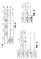
- FIG. 1 illustrates a display handler 100 in accordance with one embodiment.
- FIG. 2 illustrates the display handler 100, which provides flexibility to change the number and order of universal pixel planes (UPP) in accordance with one embodiment.
- UPP universal pixel planes
- FIG. 3 illustrates a block diagram of a universal pixel plane in accordance with one embodiment.
- FIG. 4 depicts a table 400 comprising a first combination and a second combination according to which the universal pixel planes (UPP) is to be configured in accordance with one embodiment.
- UFP universal pixel planes
- FIG. 5 illustrates UPPs configured and arranged in accordance with the first combination.
- FIG. 6 illustrates UPPs configured and arranged in accordance with the second combination.
- FIG. 7 illustrates a computer system comprising the display handler in accordance with one embodiment.
- references in the specification to "one embodiment”, “an embodiment”, “an example embodiment”, indicate that the embodiment described may include a particular feature, structure, or characteristic, but every embodiment may not necessarily include the particular feature, structure, or characteristic. Moreover, such phrases are not necessarily referring to the same embodiment. Further, when a particular feature, structure, or characteristic is described in connection with an embodiment, it is submitted that it is within the knowledge of one skilled in the art to affect such feature, structure, or characteristic in connection with other embodiments whether or not explicitly described.
- Embodiments of the invention may be implemented in hardware, firmware, software, or any combination thereof. Embodiments of the invention may also be implemented as instructions stored on a machine-readable medium, which may be read and executed by one or more processors.
- a machine-readable medium may include any mechanism for storing or transmitting information in a form readable by a machine (e.g., a computing device).
- a machine-readable medium may include read only memory (ROM); random access memory (RAM); magnetic disk storage media; optical storage media; flash memory devices; electrical, optical, acoustical or other forms of signals.
- ROM read only memory
- RAM random access memory
- the display handler 100 may comprise a video display controller 110 and a display interface 150.
- the display handler 100 may be provisioned between a host system and a display device 190.
- the display handler 100 may support High Definition Multi-media Interface (HDMI), analog component video, Phase Alternating Line (PAL) or National Television System Committee (NTSC), or Sequential Color with Memory (SECAM) standards and such other similar standard outputs to support the display device 190.
- the display device 190 may comprise a PAL/NTSC enabled television, a cathode ray tube (CRT) screen, an liquid crystal display (LCD) device, and such other similar devices.
- the graphics and/or video processing techniques described herein with reference to the display handler 100 may be implemented in various hardware architectures.
- graphics and/or video functionality may be integrated within a chipset.
- a discrete graphics and/or video processor may be used.
- the graphics and/or video functions may be implemented by a general purpose processor, including a multi-core processor.
- the functions may be implemented in a consumer electronics device such as mobile internet devices, cell phones, home entertainment devices and such other devices.
- the video display controller (VDC) 110 may comprise a control unit (CU) 112, a plurality of programmable arrays, which may be provided as universal pixel planes (UPP) 115-A to 115-K, and a VDC interface 118.
- a user may generate a standardized hardware module that may be referred to as a reference universal pixel plane (UPP).
- UPP universal pixel plane
- a user may generate the reference UPP using a hardware description language such as resistor-transistor logic (RTL) code.
- RTL resistor-transistor logic
- the user may provide combinations comprising configuration values, which may be used to generate one or more UPPs 115 by providing the reference UPP.
- the host may generate combinations comprising the configuration values using the settings defined from an architecture stand point.
- the video display controller (VDC) interface 118 may couple the VDC 110 to a memory controller using a direct interface such as SAP-ms. In one embodiment, the VDC 118 may receive commands from the control unit 112 and may support transfer of pixel data over the direct interface. In one embodiment, the direct interface may support 64 bit data transfers to transfer pixel data from the memory to the VDC 110. In one embodiment, the video display controller (VDC) interface 118 may couple the VDC 110 to a host using a host interface such as SAP-ms. In one embodiment, the VDC interface 118 may receive control data from a host and transfer the control data to the control unit 112 using the host interface. In one embodiment, the host interface may support 32 bit data transfers to transfer control data comprising configuration values, for example, from the host to the VDC 110.
- a direct interface such as SAP-ms.
- control unit (CU) 112 may retrieve pixel data stored in a memory (picture buffers) through the video display controller (VDC) interface 118.
- control unit 112 may comprise data requesters each corresponding to a UPP 115.
- the data requesters may send a request for pixel data and a logic unit of the control unit 112 may arbitrate the requests before retrieving pixel data from the memory.
- the control unit 112 may store the pixel data in designated regions of a buffer 114.
- the buffer 114 may be divided into regions and each region may be associated with a UPP 115.
- control unit 112 may retrieve video from the memory and store the video pixel data to a region of the buffer 114 associated with, for example, the UPP 115-A, which may be configured to operate as a video pixel plane. In one embodiment, the control unit 112 may retrieve graphics pixel data from the memory and store the graphics pixel data to a region of the buffer 114 associated with the UPP 115-B, for example, which may be configured to operate as a graphics pixel plane.
- the CU 112 may receive configuration values from a user of a host system and may instantiate the UPPs 115 using the configuration values.
- the configuration values may be provided as combinations and each combination may comprise data representing the number of UPPs and the order in which the UPPs may be arranged.
- the CU 112 may program the registers of a UPP 115 to render the UPP 115 as, for example, a video plane or a graphics plane.
- programming the registers of a UPP to render the UPP as a video plane or a graphics plane may provide flexibility to change the number of pixel planes and/or the order in which the pixel planes are arranged for blending.
- control unit 112 may use the configuration values of a first combination to program the registers of the UPP 115-A to 115-E to render UPPs 115-A and 115-C to 115-E as video pixel planes and UPP 115-B as a graphics pixel plane, for example.
- control unit 112 may use the configuration values of a second combination to program the registers of the UPP 115-A to 115-E to render UPP 115-A, 115-B, and 115-D as graphics pixel planes and UPP 115-C and 115-E as video pixel planes, for example.
- the number of pixel planes may be less than or more than five pixel planes and the blending order may comprise any combination of the pixel planes as specified by an architecture.
- FIG.2 An embodiment of a display handler 100, which provides flexibility to change the number and order of universal pixel planes (UPP) is illustrated in FIG.2 .
- UFP universal pixel planes
- the display handler 100 may receive configuration values over a host interface.
- the configuration values may represent a combination in which pixel planes such as video planes and graphics planes may be arranged in an order.
- the Type-1 may represent a video pixel plane and Type-2 may represent a graphics pixel plane and the blending order represents that a first plane equals video plane, a second plane equals a graphics plane, and a third, fourth, and fifth planes equal video plane.
- the display handler 100 may generate one or more universal pixel planes (UPP).
- the control unit 112 may receive configuration values representing one or more combinations and provide UPPs 115 using the configuration values.
- the control unit 112 may generate five implementations UPP 115-A, UPP 115-B, UPP 115-C, UPP 115-D and UPP 115-E using the reference UPP.
- the configuration values of a combination may comprise more than two types of UPPs as well.
- the display handler 100 may configure the universal pixel planes (UPP) using the configuration values.
- the control unit 112 may program the registers of the UPP and such programming may render a UPP as one of the Type specified by the configuration values.
- the control unit 112 may program the registers of UPP 115-A and UPP 115-C to 115-D as Type-1 and UPP 115-B as Type-2.
- the Type-1 may refer to video plane and Type-2 may refer to graphics plane.
- control unit 112 may program the configuration values (Video format: Pseudo-planar YCbCr 4:2:2 8-bit; Conversion: 4:2:2 to 4:4:4 is enabled; Scaling: disabled; Color space conversion: YCbCr to RGB is enabled and correspondingly the conversion equation coefficients are programmed; Gamma correction: Enabled, correspondingly the conversion table is programmed) in the registers of the UPP 115-A, 115-C and 115-D to render the UPPs UPP 115-A, 115-C and 115-D as video pixel planes.
- Configuration values Video format: Pseudo-planar YCbCr 4:2:2 8-bit; Conversion: 4:2:2 to 4:4:4 is enabled; Scaling: disabled; Color space conversion: YCbCr to RGB is enabled and correspondingly the conversion equation coefficients are programmed; Gamma correction: Enabled, correspondingly the conversion table is programme
- control unit 112 may program the configuration values (Video format: 32-bit ARGB (8-8-8-8); Conversion: 4:2:2 to 4:4:4 is disabled; Scaling: Enabled; Color space conversion: Disabled; Gamma correction: Disabled) in the registers of the UPP 115-B and 115-E to render the UPPs 115-B and 115-E as graphics pixel planes.
- configuration values Video format: 32-bit ARGB (8-8-8-8); Conversion: 4:2:2 to 4:4:4 is disabled; Scaling: Enabled; Color space conversion: Disabled; Gamma correction: Disabled
- the display handler 100 may process the UPPs.
- the display handler 100 may use a blender to perform blending operation on the UPPs 115-A to 115-D.
- the display handler 100 may check whether the configuration values have changed and control passes to block 260 if the configuration values (or a next combination) change and the process ends otherwise.
- the display handler 100 may reconfigure the universal pixel planes (UPP) using the changed configuration values.
- the changed configuration values may equal (T2-T2-T1). However, the number of UPPs may be less than or greater than 3 as well.
- the control unit 112 may reprogram the registers to render UPP 115-A and UPP 115-B as Type-2 and UPP 115-C as Type-1.
- the display handler 100 may change the number and order in which the UPPs may be arranged using the configuration values. Such an approach may provide flexibility in processing the pixel planes.
- the UPP 115 may comprise a UPP interface 305, programmable registers 312, a pixel extraction block 320, a format conversion block 330, a scaling block 340, a color space conversion block 350, and a gamma correction block 390.
- the UPP 115 may comprise a UPP interface 305, programmable registers 312, a pixel extraction block 320, a format conversion block 330, a scaling block 340, a color space conversion block 350, and a gamma correction block 390.
- five stages 320, 330, 340, 350, and 390 may be scheduled for each the UPP 115. However, some or all the five stages may be enabled based on the Type of the pixel plane.
- the UPP interface 305 may receive the programmable values and store the programmable values in the programmable registers 312. In one embodiment, the programmable values stored in the registers 312 may render a UPP 115 as one of the Type indicated by the configuration values. In one embodiment, the UPP interface 305 may transfer pixel data from a region of the buffer 314 associated with the UPP 115 to a pixel extraction block 320. In one embodiment, the UPP interface 305 may transfer the programmable values and pixel data to the UPP 115 as directed by the control unit 112.
- the pixel formats supported by the UPP 115 may include 8/10-bit component packed pseudo-planar YCbCr 422 format for video planes, and 32-bit ARGB (8-8-8-8); 32-bit XRGB (X-8-8-8); 16-bit ARGB (1-5-5-5 and 4-4-4-4), 16-bit RGB (5-6-5 and X-5-5-5) packed formats for graphics planes.
- the pixel extraction block 320 may extract pixels from packed bit stream retrieved from the memory and split components of the pixels. In one embodiment, the pixel extraction block 320 may receive pixel data from the region of the buffer 114 and extract the pixel data to enable pixel-by-pixel processing. In one embodiment, due to the packed nature of the stored data, the individual pixels may start at fractional byte locations. In one embodiment, there may be separate frame start addresses for Y and Cb Cr in YCbCr modes. For pixel formats that use 8 bits/component, the pixels start at the boundary of the byte. In one embodiment, the pixel extraction block 320 may extract pixels from different positions within the frame.
- the pixel extraction block 320 may also split the components of the pixels. In one embodiment, if the pixel data is in YCbCr format, the pixel extraction block 320 may split the 'Y' component and 'CbCr' components. In one embodiment, if the pixel data is in ARGB format, the pixel extraction block 320 may split alpha (A) component from the RGB components.
- the format conversion block 330 may receive the pixels from the pixel extraction block 320 and convert the pixels from one format to the other. In one embodiment, the format conversion block 330 may convert the YCbCr in 4:2:2 (422 format) to YCbCr in 4:4:4 (444 format), wherein Y is the luminance and CbCr are the chroma components. In one embodiment, the format conversion block 330 may interpolate the YCbCr in 422 format to generate YCbCr in 444 format. In one embodiment, the format conversion block 330 may comprise a 4-tap horizontal scaling to interpolate the missing U V samples in the YCbCr in 422 format. In one embodiment, the 422 to 444 conversion may comprise 1:2 upscale operations for each chroma (U and V) component.
- the scaling block 340 may provide up-scaling through pixel/line duplication.
- the control unit 112 may program a control register with a scaling factor.
- the scaling block 340 may provide Cb and Cr components of the YCbCr format with an up-scaling factor of 2, while Y component may remain unchanged.
- the scaling block 340 may replicate the alpha component and interpolate the RGB components.
- the color space conversion block 350 may perform RGB to YCbCr conversion or YCbCr to RGB conversion. In one embodiment, the color space conversion block 350 may be programmed to perform color space conversion. In one embodiment, the color space conversion block 350 may be provided with one or more inputs such as R/Cr, Y/G, and B/Cb along with one or more programmable parameters such as signed input offset values, signed co-efficient matrix values, and signed output offset range values. In one embodiment, in addition to color space conversion, the color space conversion block 350 may also perform brightness and hue/contrast adjustment.
- the gamma correction block 390 may perform gamma correction to compensate for non-linear characteristics of the display device 190 such as the cathode ray tube (CRT) of a television or a CRT based computer monitor.
- gamma correction is a pre-correction of the signal received from the color space conversion block 350.
- gamma is a parameter of light reproduction function of a CRT.
- the non-linear characteristic of a CRT may be represented by a transfer function of an approximately exponential curve referred to as a 'gamma curve'.
- the gamma correction may be approximated in hardware by implementing a piece-wise linear approximation of the gamma curve.
- the output of the gamma correction unit 390 may be provided as input to a blending unit, which blends the output from Type-1 and Type-2 UPPs.
- the table 400 comprises four columns 405, 410, 411, 412, and 413 and three rows 440, 450, and 480.
- Column 405 represents a combination identifier (Cid)
- column 410 represents quantity of type-1 UPP
- column 411 represents quantity of type-2 UPP
- column 412 represents a 'quantity value'
- column 413 represents the blending order.
- Row 450 comprises 'first combination', '4', '1', '5' and 'T1-T2-T1-T1-T1' representing combination identifier (Cid), T1, T2, and the blending order respectively.
- Row 480 comprises 'second combination', '1', '2', '3' and 'T2-T2-T1' representing combination identifier (Cid), T1, T2, 'quantity value' and the blending order respectively.
- FIG. 5 An embodiment of an arrangement of UPPs in accordance with the first combination is depicted in FIG. 5 .
- the UPP 510-1, UPP 510-3 to UPP 510-5 may be rendered as Type-1 UPP and UPP 510-2 may be rendered as Type-2 UPP.
- the UPPs 510-1 to 510-5 may be arranged to satisfy the blending order of the first combination.
- the output of UPPs 510-1 and 510-2 may be provided as inputs to a blending element 580-1.
- the output of the blending element 580-1 and the UPP 510-3 may be provided as inputs to a blending element 580-2.
- the output of the blending element 580-2 and the UPP 510-4 may be coupled to a blending element 580-3.
- the output of the blending element 580-3 and the UPP 510-5 may be provided as inputs to the blending element 580-4.
- the output of the blending element 580-4 may be referred to as the output of the blender 580.
- the blending elements 580-1 to 580-4 may collectively position the content into a window on the screen coordinates of the display device 190. Also, the blending elements 580-1 to 580-4 may collectively merge the contents from different UPP 510-1 to 510-5 based on the blending order.
- FIG. 6 An embodiment of an arrangement of UPPs in accordance with the second combination is depicted in FIG. 6 .
- the UPP 610-3 may be rendered as Type-1 UPP and the UPP 610-1 and UPP 610-2 may be rendered as Type-2 UPP.
- the UPPs 610-1 to 610-3 may be arranged to satisfy the blending order of the second combination.
- the output of UPPs 610-1 and 610-2 may be provided as inputs to a blending element 680-1.
- the output of the blending element 680-1 and the UPP 610-3 may be provided as inputs to a blending element 680-2.
- the output of the blending element 680-2 may be referred to as the output of the blender 680.
- the blending elements 680-1 to 680-2 may collectively position the content into a window on the screen coordinates of the display device 190. Also, the blending elements 680-1 to 680-2 may collectively merge the contents from different UPP 610-1 to 610-3 based on the blending order.
- a computer system 700 may include a graphics processor unit (GPU) 705, including a single instruction multiple data (SIMD) processor 710.
- the processor 710 may store a sequence of instructions, to provide and process the universal pixel planes in machine readable storage medium 725.
- the sequence of instructions may also be stored in the memory 720 or in any other suitable storage medium.
- a central processing unit 702 for the entire computer system 700 may be used to implement combinations of UPP 115 and processing of such combinations of UPPs 115, as another example.
- the central processing unit 702 that operates the computer system 700 may be one or more processor cores coupled to logic 730.
- the logic 730 for example, could be chipset logic in one embodiment.
- the logic 730 is coupled to the memory 720, which can be any kind of storage, including optical, magnetic, or semiconductor storage.
- the graphics processor unit 702 is coupled through a frame buffer 703 to a display 740.
- the GPU 705 may comprise a display handler 708.
- the GPU 705 may process the transactions and transfer the corresponding data between the memory 720, the I/O devices 760, and the display 740.
- the display handler 708 may receive configuration values from the processor 710 or the CPU 702 or from a user and provide UPPs using the configuration values.
- the display handler 708 may render the UPPs as one of the type (for example, a video or a graphics plane) using the configuration values.
- a user may use one of the I/O devices 760 to provide the configuration values.
- the processor 710 or the graphics processor unit 705 may be programmed to generate the configuration values.
- the display handler 708 may retrieve pixel data from the machine readable storage medium 725 or the memory 720 and provide the pixel data to the universal pixel planes.
- providing the UPPs and rendering the UPPs based on the configuration values to match the arrangement provided by the configuration values may provide flexibility to change the number of UPPs and the order in which the UPPs may be blended.
- graphics processing techniques described herein may be implemented in various hardware architectures. For example, graphics functionality may be integrated within a chipset. Alternatively, a discrete graphics processor may be used. As still another embodiment, the graphics functions may be implemented by a general purpose processor, including a multicore processor.
Landscapes
- Engineering & Computer Science (AREA)
- Physics & Mathematics (AREA)
- General Physics & Mathematics (AREA)
- Theoretical Computer Science (AREA)
- Computer Graphics (AREA)
- Computer Hardware Design (AREA)
- Controls And Circuits For Display Device (AREA)
- Image Processing (AREA)
Abstract
Description
- A computer system may be coupled to a display device that may allow a computer system to display visual information such as video and graphics. The computer system may process visual information before displaying the visual information on the display device. The computer system may comprise a video display controller, which may retrieve data representing various formats of visual information. Processing of data may include tasks such as conversion of data from one format to other, color space conversion, color correction, gamma correction, and encoding to suit the display format. Typically, a number of pixel planes and an order in which these pixel planes are arranged for blending are fixed for a given architecture. Having a fixed order and fixed number of pixel planes may not provide flexibility to change the order in which the pixel planes may be arranged and to change the number of a type of pixel planes used.
- The invention described herein is illustrated by way of example and not by way of limitation in the accompanying figures. For simplicity and clarity of illustration, elements illustrated in the figures are not necessarily drawn to scale. For example, the dimensions of some elements may be exaggerated relative to other elements for clarity. Further, where considered appropriate, reference labels have been repeated among the figures to indicate corresponding or analogous elements.
-
FIG. 1 illustrates adisplay handler 100 in accordance with one embodiment. -
FIG. 2 illustrates thedisplay handler 100, which provides flexibility to change the number and order of universal pixel planes (UPP) in accordance with one embodiment. -
FIG. 3 illustrates a block diagram of a universal pixel plane in accordance with one embodiment. -
FIG. 4 depicts a table 400 comprising a first combination and a second combination according to which the universal pixel planes (UPP) is to be configured in accordance with one embodiment. -
FIG. 5 illustrates UPPs configured and arranged in accordance with the first combination. -
FIG. 6 illustrates UPPs configured and arranged in accordance with the second combination. -
FIG. 7 illustrates a computer system comprising the display handler in accordance with one embodiment. - The following description describes processing pixel planes representing visual information. In the following description, numerous specific details such as logic implementations, resource partitioning, or sharing, or duplication implementations, types and interrelationships of system components, and logic partitioning or integration choices are set forth in order to provide a more thorough understanding of the present invention. It will be appreciated, however, by one skilled in the art that the invention may be practiced without such specific details. In other instances, control structures, gate level circuits, and full software instruction sequences have not been shown in detail in order not to obscure the invention. Those of ordinary skill in the art, with the included descriptions, will be able to implement appropriate functionality without undue experimentation.
- References in the specification to "one embodiment", "an embodiment", "an example embodiment", indicate that the embodiment described may include a particular feature, structure, or characteristic, but every embodiment may not necessarily include the particular feature, structure, or characteristic. Moreover, such phrases are not necessarily referring to the same embodiment. Further, when a particular feature, structure, or characteristic is described in connection with an embodiment, it is submitted that it is within the knowledge of one skilled in the art to affect such feature, structure, or characteristic in connection with other embodiments whether or not explicitly described.
- Embodiments of the invention may be implemented in hardware, firmware, software, or any combination thereof. Embodiments of the invention may also be implemented as instructions stored on a machine-readable medium, which may be read and executed by one or more processors. A machine-readable medium may include any mechanism for storing or transmitting information in a form readable by a machine (e.g., a computing device).
- For example, a machine-readable medium may include read only memory (ROM); random access memory (RAM); magnetic disk storage media; optical storage media; flash memory devices; electrical, optical, acoustical or other forms of signals. Further, firmware, software, routines, and instructions may be described herein as performing certain actions. However, it should be appreciated that such descriptions are merely for convenience and that such actions in fact result from computing devices, processors, controllers, and other devices executing the firmware, software, routines, and instructions.
- An embodiment of a
display handler 100 is illustrated inFIG. 1 . Thedisplay handler 100 may comprise avideo display controller 110 and adisplay interface 150. Thedisplay handler 100 may be provisioned between a host system and adisplay device 190. In one embodiment, thedisplay handler 100 may support High Definition Multi-media Interface (HDMI), analog component video, Phase Alternating Line (PAL) or National Television System Committee (NTSC), or Sequential Color with Memory (SECAM) standards and such other similar standard outputs to support thedisplay device 190. In one embodiment, thedisplay device 190 may comprise a PAL/NTSC enabled television, a cathode ray tube (CRT) screen, an liquid crystal display (LCD) device, and such other similar devices. In one embodiment, the graphics and/or video processing techniques described herein with reference to thedisplay handler 100 may be implemented in various hardware architectures. - For example, graphics and/or video functionality may be integrated within a chipset. Alternatively, a discrete graphics and/or video processor may be used. As still another embodiment, the graphics and/or video functions may be implemented by a general purpose processor, including a multi-core processor. In a further embodiment, the functions may be implemented in a consumer electronics device such as mobile internet devices, cell phones, home entertainment devices and such other devices.
- In one embodiment, the video display controller (VDC) 110 may comprise a control unit (CU) 112, a plurality of programmable arrays, which may be provided as universal pixel planes (UPP) 115-A to 115-K, and a
VDC interface 118. In one embodiment, a user may generate a standardized hardware module that may be referred to as a reference universal pixel plane (UPP). In one embodiment, a user may generate the reference UPP using a hardware description language such as resistor-transistor logic (RTL) code. In one embodiment, the user may provide combinations comprising configuration values, which may be used to generate one ormore UPPs 115 by providing the reference UPP. In other embodiment, the host may generate combinations comprising the configuration values using the settings defined from an architecture stand point. - In one embodiment, the video display controller (VDC)
interface 118 may couple the VDC 110 to a memory controller using a direct interface such as SAP-ms. In one embodiment, the VDC 118 may receive commands from thecontrol unit 112 and may support transfer of pixel data over the direct interface. In one embodiment, the direct interface may support 64 bit data transfers to transfer pixel data from the memory to theVDC 110. In one embodiment, the video display controller (VDC)interface 118 may couple the VDC 110 to a host using a host interface such as SAP-ms. In one embodiment, theVDC interface 118 may receive control data from a host and transfer the control data to thecontrol unit 112 using the host interface. In one embodiment, the host interface may support 32 bit data transfers to transfer control data comprising configuration values, for example, from the host to theVDC 110. - In one embodiment, the control unit (CU) 112 may retrieve pixel data stored in a memory (picture buffers) through the video display controller (VDC)
interface 118. In one embodiment,control unit 112 may comprise data requesters each corresponding to aUPP 115. In one embodiment, the data requesters may send a request for pixel data and a logic unit of thecontrol unit 112 may arbitrate the requests before retrieving pixel data from the memory. In one embodiment, thecontrol unit 112 may store the pixel data in designated regions of abuffer 114. In one embodiment, thebuffer 114 may be divided into regions and each region may be associated with aUPP 115. - In one embodiment, the
control unit 112 may retrieve video from the memory and store the video pixel data to a region of thebuffer 114 associated with, for example, the UPP 115-A, which may be configured to operate as a video pixel plane. In one embodiment, thecontrol unit 112 may retrieve graphics pixel data from the memory and store the graphics pixel data to a region of thebuffer 114 associated with the UPP 115-B, for example, which may be configured to operate as a graphics pixel plane. - In one embodiment, the
CU 112 may receive configuration values from a user of a host system and may instantiate theUPPs 115 using the configuration values. In one embodiment, the configuration values may be provided as combinations and each combination may comprise data representing the number of UPPs and the order in which the UPPs may be arranged. In one embodiment, the CU 112 may program the registers of a UPP 115 to render the UPP 115 as, for example, a video plane or a graphics plane. In one embodiment, programming the registers of a UPP to render the UPP as a video plane or a graphics plane may provide flexibility to change the number of pixel planes and/or the order in which the pixel planes are arranged for blending. - In one embodiment, the
control unit 112 may use the configuration values of a first combination to program the registers of the UPP 115-A to 115-E to render UPPs 115-A and 115-C to 115-E as video pixel planes and UPP 115-B as a graphics pixel plane, for example. In other embodiment, thecontrol unit 112 may use the configuration values of a second combination to program the registers of the UPP 115-A to 115-E to render UPP 115-A, 115-B, and 115-D as graphics pixel planes and UPP 115-C and 115-E as video pixel planes, for example. In one embodiment, the number of pixel planes may be less than or more than five pixel planes and the blending order may comprise any combination of the pixel planes as specified by an architecture. - An embodiment of a
display handler 100, which provides flexibility to change the number and order of universal pixel planes (UPP) is illustrated inFIG.2 . - In
block 210, thedisplay handler 100 may receive configuration values over a host interface. In one embodiment, the configuration values may represent a combination in which pixel planes such as video planes and graphics planes may be arranged in an order. For example, a first combination may comprise Type-1 quantity = 4, Type-2 quantity =1 and blending order = T1-T2-T1-T1-T1. In one embodiment, the Type-1 may represent a video pixel plane and Type-2 may represent a graphics pixel plane and the blending order represents that a first plane equals video plane, a second plane equals a graphics plane, and a third, fourth, and fifth planes equal video plane. - In
block 220, thedisplay handler 100 may generate one or more universal pixel planes (UPP). In one embodiment, thecontrol unit 112 may receive configuration values representing one or more combinations and provideUPPs 115 using the configuration values. In one embodiment, the number of UPPs (=5) provided by thecontrol unit 112 may equal a sum of Type-1 quantity (=4, for example) and Type-2 quantity (=1, for example). In one embodiment, thecontrol unit 112 may generate five implementations UPP 115-A, UPP 115-B, UPP 115-C, UPP 115-D and UPP 115-E using the reference UPP. In one embodiment, the configuration values of a combination may comprise more than two types of UPPs as well. - In
block 230, thedisplay handler 100 may configure the universal pixel planes (UPP) using the configuration values. In one embodiment, thecontrol unit 112 may program the registers of the UPP and such programming may render a UPP as one of the Type specified by the configuration values. In one embodiment, using the contents of the blending order field (=T1-T2-T1-T1-T1) of the first combination, thecontrol unit 112 may program the registers of UPP 115-A and UPP 115-C to 115-D as Type-1 and UPP 115-B as Type-2. In one embodiment, the Type-1 may refer to video plane and Type-2 may refer to graphics plane. - In one embodiment, the
control unit 112 may program the configuration values (Video format: Pseudo-planar YCbCr 4:2:2 8-bit; Conversion: 4:2:2 to 4:4:4 is enabled; Scaling: disabled; Color space conversion: YCbCr to RGB is enabled and correspondingly the conversion equation coefficients are programmed; Gamma correction: Enabled, correspondingly the conversion table is programmed) in the registers of the UPP 115-A, 115-C and 115-D to render the UPPs UPP 115-A, 115-C and 115-D as video pixel planes. - In one embodiment, the
control unit 112 may program the configuration values (Video format: 32-bit ARGB (8-8-8-8); Conversion: 4:2:2 to 4:4:4 is disabled; Scaling: Enabled; Color space conversion: Disabled; Gamma correction: Disabled) in the registers of the UPP 115-B and 115-E to render the UPPs 115-B and 115-E as graphics pixel planes. - In
block 240, thedisplay handler 100 may process the UPPs. In one embodiment, thedisplay handler 100 may use a blender to perform blending operation on the UPPs 115-A to 115-D. - In
block 250, thedisplay handler 100 may check whether the configuration values have changed and control passes to block 260 if the configuration values (or a next combination) change and the process ends otherwise. - In
block 260, thedisplay handler 100 may reconfigure the universal pixel planes (UPP) using the changed configuration values. In one embodiment, the changed configuration values may equal (T2-T2-T1). However, the number of UPPs may be less than or greater than 3 as well. In one embodiment, thecontrol unit 112 may reprogram the registers to render UPP 115-A and UPP 115-B as Type-2 and UPP 115-C as Type-1. In one embodiment, thedisplay handler 100 may change the number and order in which the UPPs may be arranged using the configuration values. Such an approach may provide flexibility in processing the pixel planes. - An embodiment of a universal pixel plane (UPP) 115 is illustrated in
FIG. 3 . In one embodiment, theUPP 115 may comprise aUPP interface 305,programmable registers 312, apixel extraction block 320, aformat conversion block 330, ascaling block 340, a colorspace conversion block 350, and agamma correction block 390. In one embodiment, fivestages UPP 115. However, some or all the five stages may be enabled based on the Type of the pixel plane. - In one embodiment, the
UPP interface 305 may receive the programmable values and store the programmable values in the programmable registers 312. In one embodiment, the programmable values stored in theregisters 312 may render aUPP 115 as one of the Type indicated by the configuration values. In one embodiment, theUPP interface 305 may transfer pixel data from a region of the buffer 314 associated with theUPP 115 to apixel extraction block 320. In one embodiment, theUPP interface 305 may transfer the programmable values and pixel data to theUPP 115 as directed by thecontrol unit 112. - In one embodiment, the pixel formats supported by the
UPP 115 may include 8/10-bit component packed pseudo-planar YCbCr 422 format for video planes, and 32-bit ARGB (8-8-8-8); 32-bit XRGB (X-8-8-8); 16-bit ARGB (1-5-5-5 and 4-4-4-4), 16-bit RGB (5-6-5 and X-5-5-5) packed formats for graphics planes. - In one embodiment, the
pixel extraction block 320 may extract pixels from packed bit stream retrieved from the memory and split components of the pixels. In one embodiment, thepixel extraction block 320 may receive pixel data from the region of thebuffer 114 and extract the pixel data to enable pixel-by-pixel processing. In one embodiment, due to the packed nature of the stored data, the individual pixels may start at fractional byte locations. In one embodiment, there may be separate frame start addresses for Y and Cb Cr in YCbCr modes. For pixel formats that use 8 bits/component, the pixels start at the boundary of the byte. In one embodiment, thepixel extraction block 320 may extract pixels from different positions within the frame. - In one embodiment, the
pixel extraction block 320 may also split the components of the pixels. In one embodiment, if the pixel data is in YCbCr format, thepixel extraction block 320 may split the 'Y' component and 'CbCr' components. In one embodiment, if the pixel data is in ARGB format, thepixel extraction block 320 may split alpha (A) component from the RGB components. - In one embodiment, the
format conversion block 330 may receive the pixels from thepixel extraction block 320 and convert the pixels from one format to the other. In one embodiment, theformat conversion block 330 may convert the YCbCr in 4:2:2 (422 format) to YCbCr in 4:4:4 (444 format), wherein Y is the luminance and CbCr are the chroma components. In one embodiment, theformat conversion block 330 may interpolate the YCbCr in 422 format to generate YCbCr in 444 format. In one embodiment, theformat conversion block 330 may comprise a 4-tap horizontal scaling to interpolate the missing U V samples in the YCbCr in 422 format. In one embodiment, the 422 to 444 conversion may comprise 1:2 upscale operations for each chroma (U and V) component. - In one embodiment, the
scaling block 340 may provide up-scaling through pixel/line duplication. In one embodiment, thecontrol unit 112 may program a control register with a scaling factor. In one embodiment, thescaling block 340 may provide Cb and Cr components of the YCbCr format with an up-scaling factor of 2, while Y component may remain unchanged. In one embodiment, if thescaling block 340 receives alpha and RGB components, thescaling block 340 may replicate the alpha component and interpolate the RGB components. - In one embodiment, the color
space conversion block 350 may perform RGB to YCbCr conversion or YCbCr to RGB conversion. In one embodiment, the colorspace conversion block 350 may be programmed to perform color space conversion. In one embodiment, the colorspace conversion block 350 may be provided with one or more inputs such as R/Cr, Y/G, and B/Cb along with one or more programmable parameters such as signed input offset values, signed co-efficient matrix values, and signed output offset range values. In one embodiment, in addition to color space conversion, the colorspace conversion block 350 may also perform brightness and hue/contrast adjustment. - In one embodiment, the
gamma correction block 390 may perform gamma correction to compensate for non-linear characteristics of thedisplay device 190 such as the cathode ray tube (CRT) of a television or a CRT based computer monitor. In one embodiment, gamma correction is a pre-correction of the signal received from the colorspace conversion block 350. In one embodiment, gamma is a parameter of light reproduction function of a CRT. In one embodiment, the non-linear characteristic of a CRT may be represented by a transfer function of an approximately exponential curve referred to as a 'gamma curve'. In one embodiment, the gamma correction may be approximated in hardware by implementing a piece-wise linear approximation of the gamma curve. In one embodiment, the output of thegamma correction unit 390 may be provided as input to a blending unit, which blends the output from Type-1 and Type-2 UPPs. - An embodiment of the configuration values represented as one or more combinations is depicted in a table 400 of
FIG. 4 . In one embodiment, the table 400 comprises fourcolumns rows Column 405 represents a combination identifier (Cid),column 410 represents quantity of type-1 UPP, Type-1 (T1) quantity,column 411 represents quantity of type-2 UPP, Type-2 (T2) quantity,column 412 represents a 'quantity value', andcolumn 413 represents the blending order. - Row 450 comprises 'first combination', '4', '1', '5' and 'T1-T2-T1-T1-T1' representing combination identifier (Cid), T1, T2, and the blending order respectively. In one embodiment, the
control unit 112 may use the configuration values such as the quantity value (=5) to provide five UPPs 115-A to 115-E and then program the UPP 115-A and 115-C to 115-E as Type-1 universal pixel planes and UPP 115-B as Type-2 universal pixel plane. - Row 480 comprises 'second combination', '1', '2', '3' and 'T2-T2-T1' representing combination identifier (Cid), T1, T2, 'quantity value' and the blending order respectively. In one embodiment, the
control unit 112 may use the configuration values such as the quantity value (=3) of the second combination to provide three UPPs 115-A to 115-C and then program the UPP 115-A and 115-B as Type-2 universal pixel planes and UPP 115-C as Type-1 universal pixel plane. - An embodiment of an arrangement of UPPs in accordance with the first combination is depicted in
FIG. 5 . In accordance with the blending order, the UPP 510-1, UPP 510-3 to UPP 510-5 may be rendered as Type-1 UPP and UPP 510-2 may be rendered as Type-2 UPP. In one embodiment, the UPPs 510-1 to 510-5 may be arranged to satisfy the blending order of the first combination. - In one embodiment, the output of UPPs 510-1 and 510-2 may be provided as inputs to a blending element 580-1. In one embodiment, the output of the blending element 580-1 and the UPP 510-3 may be provided as inputs to a blending element 580-2. In one embodiment, the output of the blending element 580-2 and the UPP 510-4 may be coupled to a blending element 580-3. In one embodiment, the output of the blending element 580-3 and the UPP 510-5 may be provided as inputs to the blending element 580-4. In one embodiment, the output of the blending element 580-4 may be referred to as the output of the
blender 580. In one embodiment, the blending elements 580-1 to 580-4 may collectively position the content into a window on the screen coordinates of thedisplay device 190. Also, the blending elements 580-1 to 580-4 may collectively merge the contents from different UPP 510-1 to 510-5 based on the blending order. - An embodiment of an arrangement of UPPs in accordance with the second combination is depicted in
FIG. 6 . In accordance with the blending order, the UPP 610-3 may be rendered as Type-1 UPP and the UPP 610-1 and UPP 610-2 may be rendered as Type-2 UPP. In one embodiment, the UPPs 610-1 to 610-3 may be arranged to satisfy the blending order of the second combination. - In one embodiment, the output of UPPs 610-1 and 610-2 may be provided as inputs to a blending element 680-1. In one embodiment, the output of the blending element 680-1 and the UPP 610-3 may be provided as inputs to a blending element 680-2. In one embodiment, the output of the blending element 680-2 may be referred to as the output of the
blender 680. In one embodiment, the blending elements 680-1 to 680-2 may collectively position the content into a window on the screen coordinates of thedisplay device 190. Also, the blending elements 680-1 to 680-2 may collectively merge the contents from different UPP 610-1 to 610-3 based on the blending order. - Referring to
FIG. 7 , acomputer system 700 may include a graphics processor unit (GPU) 705, including a single instruction multiple data (SIMD)processor 710. Theprocessor 710, in one embodiment, may store a sequence of instructions, to provide and process the universal pixel planes in machine readable storage medium 725. However, the sequence of instructions may also be stored in thememory 720 or in any other suitable storage medium. - While a separate
graphics processor unit 705 is depicted inFig. 7 , in some embodiments, acentral processing unit 702 for theentire computer system 700 may be used to implement combinations ofUPP 115 and processing of such combinations ofUPPs 115, as another example. Thecentral processing unit 702 that operates thecomputer system 700 may be one or more processor cores coupled tologic 730. Thelogic 730, for example, could be chipset logic in one embodiment. Thelogic 730 is coupled to thememory 720, which can be any kind of storage, including optical, magnetic, or semiconductor storage. Thegraphics processor unit 702 is coupled through aframe buffer 703 to adisplay 740. - In one embodiment, the
GPU 705 may comprise adisplay handler 708. In one embodiment, theGPU 705 may process the transactions and transfer the corresponding data between thememory 720, the I/O devices 760, and thedisplay 740. In one embodiment, thedisplay handler 708 may receive configuration values from theprocessor 710 or theCPU 702 or from a user and provide UPPs using the configuration values. In one embodiment, thedisplay handler 708 may render the UPPs as one of the type (for example, a video or a graphics plane) using the configuration values. In one embodiment, a user may use one of the I/O devices 760 to provide the configuration values. In other embodiment, theprocessor 710 or thegraphics processor unit 705 may be programmed to generate the configuration values. - In one embodiment, the
display handler 708 may retrieve pixel data from the machine readable storage medium 725 or thememory 720 and provide the pixel data to the universal pixel planes. In one embodiment, providing the UPPs and rendering the UPPs based on the configuration values to match the arrangement provided by the configuration values may provide flexibility to change the number of UPPs and the order in which the UPPs may be blended. - The graphics processing techniques described herein may be implemented in various hardware architectures. For example, graphics functionality may be integrated within a chipset. Alternatively, a discrete graphics processor may be used. As still another embodiment, the graphics functions may be implemented by a general purpose processor, including a multicore processor.
Claims (12)
- A method comprising:receiving a first set of configuration values, wherein the first set of configuration values include a first quantity value and a first blending order providing a first set of universal pixel planes using a reference pixel plane, wherein the number of universal pixel planes in the first set is determined using the first quantity value,rendering universal pixel planes of the first set of universal pixel planes as a type indicated by a matching element of the first blending order.
- The method of claim 1, wherein the first set comprises a first, second, third, fourth, and a fifth universal pixel plane and the first blending order comprises a first, second, third, fourth, and a fifth element, wherein the first, second, third, fourth, and a fifth element indicates a type in which the first, second, third, fourth, and a fifth universal pixel plane is to be rendered.
- The method of claim 2, wherein the first, third, fourth, and fifth universal pixel planes are of first type as indicated by the first, third, fourth, and the fifth element and the second universal pixel plane is of second type as indicated by the second element.
- The method of claim 3, wherein the first, third, fourth, and fifth universal pixel planes are rendered as the first type and the second universal pixel plane is rendered as the second type by programming each of the first set of universal pixel planes.
- The method of claim 2, wherein the first, third, fourth, and fifth universal pixel planes are rendered as video pixel planes and the second universal pixel plane is rendered as a graphics pixel plane.
- The method of claim 1 comprising:receiving a second set of configuration values, wherein the second set of configuration values include a second quantity value and a second blending orderproviding a second set of universal pixel planes using the reference pixel plane, wherein the number of universal pixel planes in the second set is determined using the second quantity value,rendering universal pixel planes of the second set of universal pixel planes as a type indicated by a matching element of the second blending order.
- The method of claim 6, wherein the second set comprises a first, second, and third universal pixel planes and the second blending order comprises a first, second, and third element, wherein the first, second, and third, element indicates a type in which the first, second, and third universal pixel plane is to be rendered.
- The method of claim 7, wherein the first and the second universal pixel planes are of second type as indicated by the first and the second element and the third universal pixel plane is of first type as indicated by the third element.
- The method of claim 7, wherein the first and second universal pixel planes are rendered as graphics pixel planes and the second universal pixel plane is rendered as the video pixel plane by programming registers of the second set of universal pixel planes.
- A machine-readable storage medium comprising a plurality of instructions that in response to being executed result in a processor performing a method as claimed in any one of claims 1 to 9.
- An apparatus comprising:an interface,a control unit coupled to the interface, anda plurality of programmable arrays coupled to the control unit,wherein the control unit is to
receive a first set of configuration values over the interface, wherein the first set of configuration values include a first quantity value and a first blending order
provide the plurality of programmable arrays as a first set of universal pixel planes using a reference pixel plane, wherein the number of universal pixel planes in the first set is determined using the first quantity value, and
render universal pixel planes of the first set of universal pixel planes as a type indicated by a matching element of the first blending order. - The apparatus of claim 11 that is operable to perform the method of any one of claims 2 to 10.
Applications Claiming Priority (1)
| Application Number | Priority Date | Filing Date | Title |
|---|---|---|---|
| US12/236,320 US8681167B2 (en) | 2008-09-23 | 2008-09-23 | Processing pixel planes representing visual information |
Publications (2)
| Publication Number | Publication Date |
|---|---|
| EP2166534A1 true EP2166534A1 (en) | 2010-03-24 |
| EP2166534B1 EP2166534B1 (en) | 2015-03-11 |
Family
ID=41508153
Family Applications (1)
| Application Number | Title | Priority Date | Filing Date |
|---|---|---|---|
| EP09252255.6A Not-in-force EP2166534B1 (en) | 2008-09-23 | 2009-09-22 | Processing pixel planes representing visual information |
Country Status (3)
| Country | Link |
|---|---|
| US (1) | US8681167B2 (en) |
| EP (1) | EP2166534B1 (en) |
| CN (1) | CN101714072B (en) |
Families Citing this family (2)
| Publication number | Priority date | Publication date | Assignee | Title |
|---|---|---|---|---|
| US20130222411A1 (en) * | 2012-02-28 | 2013-08-29 | Brijesh Tripathi | Extended range color space |
| GB202202905D0 (en) * | 2022-03-02 | 2022-04-13 | Graphcore Ltd | Processing device for intermediate value scaling |
Citations (3)
| Publication number | Priority date | Publication date | Assignee | Title |
|---|---|---|---|---|
| US6624816B1 (en) * | 1999-09-10 | 2003-09-23 | Intel Corporation | Method and apparatus for scalable image processing |
| US20050270297A1 (en) | 2004-06-08 | 2005-12-08 | Sony Corporation And Sony Electronics Inc. | Time sliced architecture for graphics display system |
| US20060244758A1 (en) | 2005-04-29 | 2006-11-02 | Modviz, Inc. | Transparency-conserving method to generate and blend images |
Family Cites Families (4)
| Publication number | Priority date | Publication date | Assignee | Title |
|---|---|---|---|---|
| US5448053A (en) * | 1993-03-01 | 1995-09-05 | Rhoads; Geoffrey B. | Method and apparatus for wide field distortion-compensated imaging |
| AU5556496A (en) * | 1995-05-09 | 1996-11-29 | Apple Computer, Inc. | Method and apparatus for compressing image data |
| KR101109960B1 (en) * | 2004-01-13 | 2012-03-13 | 파나소닉 주식회사 | Recording medium, reproduction device, recording method, and reproduction method |
| SG137754A1 (en) * | 2006-05-12 | 2007-12-28 | Nvidia Corp | Antialiasing using multiple display heads of a graphics processor |
-
2008
- 2008-09-23 US US12/236,320 patent/US8681167B2/en not_active Expired - Fee Related
-
2009
- 2009-09-22 EP EP09252255.6A patent/EP2166534B1/en not_active Not-in-force
- 2009-09-23 CN CN200910221477.1A patent/CN101714072B/en not_active Expired - Fee Related
Patent Citations (3)
| Publication number | Priority date | Publication date | Assignee | Title |
|---|---|---|---|---|
| US6624816B1 (en) * | 1999-09-10 | 2003-09-23 | Intel Corporation | Method and apparatus for scalable image processing |
| US20050270297A1 (en) | 2004-06-08 | 2005-12-08 | Sony Corporation And Sony Electronics Inc. | Time sliced architecture for graphics display system |
| US20060244758A1 (en) | 2005-04-29 | 2006-11-02 | Modviz, Inc. | Transparency-conserving method to generate and blend images |
Non-Patent Citations (1)
| Title |
|---|
| NVIDIA CORPORATION: "NVIDIA GeForce 8800 Architecture Technical Brief", NVIDIA GEFORCE 8800 ARCHITECTURE TECHNICAL BRIEF, 8 November 2006 (2006-11-08), Internet, XP002564022 * |
Also Published As
| Publication number | Publication date |
|---|---|
| CN101714072A (en) | 2010-05-26 |
| CN101714072B (en) | 2016-02-10 |
| US8681167B2 (en) | 2014-03-25 |
| EP2166534B1 (en) | 2015-03-11 |
| US20100073386A1 (en) | 2010-03-25 |
Similar Documents
| Publication | Publication Date | Title |
|---|---|---|
| US9471955B2 (en) | Multiple display pipelines driving a divided display | |
| US20130057567A1 (en) | Color Space Conversion for Mirror Mode | |
| US9001274B2 (en) | Image processing method | |
| US20120218277A1 (en) | Display list mechanism and scalable display engine structures | |
| TWI550557B (en) | Video data compression format | |
| KR20040000151A (en) | Apparatus and Method For Converting Of Pixels From YUV TO RGB Format Using Color Look-Up Tables | |
| US8717391B2 (en) | User interface pipe scalers with active regions | |
| US20160307540A1 (en) | Linear scaling in a display pipeline | |
| US7050065B1 (en) | Minimalist color space converters for optimizing image processing operations | |
| US6989837B2 (en) | System and method for processing memory with YCbCr 4:2:0 planar video data format | |
| US20060050076A1 (en) | Apparatus for and method of generating graphic data, and information recording medium | |
| US9020044B2 (en) | Method and apparatus for writing video data in raster order and reading video data in macroblock order | |
| US7554563B2 (en) | Video display control apparatus and video display control method | |
| JP2015516584A (en) | Extended range color space | |
| US8773457B2 (en) | Color space conversion | |
| EP2166534B1 (en) | Processing pixel planes representing visual information | |
| US9412147B2 (en) | Display pipe line buffer sharing | |
| US12462729B2 (en) | Mux-free architecture for pixel data bus latching in foveated displays | |
| US9953591B1 (en) | Managing two dimensional structured noise when driving a display with multiple display pipes | |
| CN118887889A (en) | Image display control system and image display control method | |
| US20150062134A1 (en) | Parameter fifo for configuring video related settings | |
| US9691349B2 (en) | Source pixel component passthrough | |
| JP4998145B2 (en) | Image processing apparatus, image processing method, image processing program, recording medium storing image processing program, and image display apparatus | |
| US9747658B2 (en) | Arbitration method for multi-request display pipeline | |
| EP1741282A1 (en) | Method and apparatus for vertically scaling pixel data |
Legal Events
| Date | Code | Title | Description |
|---|---|---|---|
| PUAI | Public reference made under article 153(3) epc to a published international application that has entered the european phase |
Free format text: ORIGINAL CODE: 0009012 |
|
| 17P | Request for examination filed |
Effective date: 20091007 |
|
| AK | Designated contracting states |
Kind code of ref document: A1 Designated state(s): AT BE BG CH CY CZ DE DK EE ES FI FR GB GR HR HU IE IS IT LI LT LU LV MC MK MT NL NO PL PT RO SE SI SK SM TR |
|
| AX | Request for extension of the european patent |
Extension state: AL BA RS |
|
| 17Q | First examination report despatched |
Effective date: 20100310 |
|
| GRAP | Despatch of communication of intention to grant a patent |
Free format text: ORIGINAL CODE: EPIDOSNIGR1 |
|
| RAP1 | Party data changed (applicant data changed or rights of an application transferred) |
Owner name: INTEL CORPORATION |
|
| INTG | Intention to grant announced |
Effective date: 20141106 |
|
| GRAS | Grant fee paid |
Free format text: ORIGINAL CODE: EPIDOSNIGR3 |
|
| GRAA | (expected) grant |
Free format text: ORIGINAL CODE: 0009210 |
|
| AK | Designated contracting states |
Kind code of ref document: B1 Designated state(s): AT BE BG CH CY CZ DE DK EE ES FI FR GB GR HR HU IE IS IT LI LT LU LV MC MK MT NL NO PL PT RO SE SI SK SM TR |
|
| REG | Reference to a national code |
Ref country code: GB Ref legal event code: FG4D |
|
| REG | Reference to a national code |
Ref country code: CH Ref legal event code: EP |
|
| REG | Reference to a national code |
Ref country code: IE Ref legal event code: FG4D |
|
| REG | Reference to a national code |
Ref country code: AT Ref legal event code: REF Ref document number: 715699 Country of ref document: AT Kind code of ref document: T Effective date: 20150415 |
|
| REG | Reference to a national code |
Ref country code: DE Ref legal event code: R096 Ref document number: 602009029911 Country of ref document: DE Effective date: 20150423 |
|
| REG | Reference to a national code |
Ref country code: NL Ref legal event code: VDEP Effective date: 20150311 |
|
| REG | Reference to a national code |
Ref country code: NL Ref legal event code: VDEP Effective date: 20150311 |
|
| PG25 | Lapsed in a contracting state [announced via postgrant information from national office to epo] |
Ref country code: ES Free format text: LAPSE BECAUSE OF FAILURE TO SUBMIT A TRANSLATION OF THE DESCRIPTION OR TO PAY THE FEE WITHIN THE PRESCRIBED TIME-LIMIT Effective date: 20150311 Ref country code: LT Free format text: LAPSE BECAUSE OF FAILURE TO SUBMIT A TRANSLATION OF THE DESCRIPTION OR TO PAY THE FEE WITHIN THE PRESCRIBED TIME-LIMIT Effective date: 20150311 Ref country code: HR Free format text: LAPSE BECAUSE OF FAILURE TO SUBMIT A TRANSLATION OF THE DESCRIPTION OR TO PAY THE FEE WITHIN THE PRESCRIBED TIME-LIMIT Effective date: 20150311 Ref country code: FI Free format text: LAPSE BECAUSE OF FAILURE TO SUBMIT A TRANSLATION OF THE DESCRIPTION OR TO PAY THE FEE WITHIN THE PRESCRIBED TIME-LIMIT Effective date: 20150311 Ref country code: NO Free format text: LAPSE BECAUSE OF FAILURE TO SUBMIT A TRANSLATION OF THE DESCRIPTION OR TO PAY THE FEE WITHIN THE PRESCRIBED TIME-LIMIT Effective date: 20150611 Ref country code: SE Free format text: LAPSE BECAUSE OF FAILURE TO SUBMIT A TRANSLATION OF THE DESCRIPTION OR TO PAY THE FEE WITHIN THE PRESCRIBED TIME-LIMIT Effective date: 20150311 |
|
| REG | Reference to a national code |
Ref country code: AT Ref legal event code: MK05 Ref document number: 715699 Country of ref document: AT Kind code of ref document: T Effective date: 20150311 |
|
| REG | Reference to a national code |
Ref country code: LT Ref legal event code: MG4D |
|
| PG25 | Lapsed in a contracting state [announced via postgrant information from national office to epo] |
Ref country code: GR Free format text: LAPSE BECAUSE OF FAILURE TO SUBMIT A TRANSLATION OF THE DESCRIPTION OR TO PAY THE FEE WITHIN THE PRESCRIBED TIME-LIMIT Effective date: 20150612 Ref country code: LV Free format text: LAPSE BECAUSE OF FAILURE TO SUBMIT A TRANSLATION OF THE DESCRIPTION OR TO PAY THE FEE WITHIN THE PRESCRIBED TIME-LIMIT Effective date: 20150311 |
|
| PG25 | Lapsed in a contracting state [announced via postgrant information from national office to epo] |
Ref country code: NL Free format text: LAPSE BECAUSE OF FAILURE TO SUBMIT A TRANSLATION OF THE DESCRIPTION OR TO PAY THE FEE WITHIN THE PRESCRIBED TIME-LIMIT Effective date: 20150311 |
|
| PG25 | Lapsed in a contracting state [announced via postgrant information from national office to epo] |
Ref country code: RO Free format text: LAPSE BECAUSE OF FAILURE TO SUBMIT A TRANSLATION OF THE DESCRIPTION OR TO PAY THE FEE WITHIN THE PRESCRIBED TIME-LIMIT Effective date: 20150311 Ref country code: EE Free format text: LAPSE BECAUSE OF FAILURE TO SUBMIT A TRANSLATION OF THE DESCRIPTION OR TO PAY THE FEE WITHIN THE PRESCRIBED TIME-LIMIT Effective date: 20150311 Ref country code: PT Free format text: LAPSE BECAUSE OF FAILURE TO SUBMIT A TRANSLATION OF THE DESCRIPTION OR TO PAY THE FEE WITHIN THE PRESCRIBED TIME-LIMIT Effective date: 20150713 Ref country code: CZ Free format text: LAPSE BECAUSE OF FAILURE TO SUBMIT A TRANSLATION OF THE DESCRIPTION OR TO PAY THE FEE WITHIN THE PRESCRIBED TIME-LIMIT Effective date: 20150311 Ref country code: SK Free format text: LAPSE BECAUSE OF FAILURE TO SUBMIT A TRANSLATION OF THE DESCRIPTION OR TO PAY THE FEE WITHIN THE PRESCRIBED TIME-LIMIT Effective date: 20150311 |
|
| PG25 | Lapsed in a contracting state [announced via postgrant information from national office to epo] |
Ref country code: PL Free format text: LAPSE BECAUSE OF FAILURE TO SUBMIT A TRANSLATION OF THE DESCRIPTION OR TO PAY THE FEE WITHIN THE PRESCRIBED TIME-LIMIT Effective date: 20150311 Ref country code: AT Free format text: LAPSE BECAUSE OF FAILURE TO SUBMIT A TRANSLATION OF THE DESCRIPTION OR TO PAY THE FEE WITHIN THE PRESCRIBED TIME-LIMIT Effective date: 20150311 Ref country code: IS Free format text: LAPSE BECAUSE OF FAILURE TO SUBMIT A TRANSLATION OF THE DESCRIPTION OR TO PAY THE FEE WITHIN THE PRESCRIBED TIME-LIMIT Effective date: 20150711 |
|
| REG | Reference to a national code |
Ref country code: DE Ref legal event code: R097 Ref document number: 602009029911 Country of ref document: DE |
|
| PG25 | Lapsed in a contracting state [announced via postgrant information from national office to epo] |
Ref country code: IT Free format text: LAPSE BECAUSE OF FAILURE TO SUBMIT A TRANSLATION OF THE DESCRIPTION OR TO PAY THE FEE WITHIN THE PRESCRIBED TIME-LIMIT Effective date: 20150311 |
|
| PLBE | No opposition filed within time limit |
Free format text: ORIGINAL CODE: 0009261 |
|
| STAA | Information on the status of an ep patent application or granted ep patent |
Free format text: STATUS: NO OPPOSITION FILED WITHIN TIME LIMIT |
|
| PG25 | Lapsed in a contracting state [announced via postgrant information from national office to epo] |
Ref country code: DK Free format text: LAPSE BECAUSE OF FAILURE TO SUBMIT A TRANSLATION OF THE DESCRIPTION OR TO PAY THE FEE WITHIN THE PRESCRIBED TIME-LIMIT Effective date: 20150311 |
|
| 26N | No opposition filed |
Effective date: 20151214 |
|
| PG25 | Lapsed in a contracting state [announced via postgrant information from national office to epo] |
Ref country code: SI Free format text: LAPSE BECAUSE OF FAILURE TO SUBMIT A TRANSLATION OF THE DESCRIPTION OR TO PAY THE FEE WITHIN THE PRESCRIBED TIME-LIMIT Effective date: 20150311 |
|
| PG25 | Lapsed in a contracting state [announced via postgrant information from national office to epo] |
Ref country code: MC Free format text: LAPSE BECAUSE OF FAILURE TO SUBMIT A TRANSLATION OF THE DESCRIPTION OR TO PAY THE FEE WITHIN THE PRESCRIBED TIME-LIMIT Effective date: 20150311 Ref country code: LU Free format text: LAPSE BECAUSE OF FAILURE TO SUBMIT A TRANSLATION OF THE DESCRIPTION OR TO PAY THE FEE WITHIN THE PRESCRIBED TIME-LIMIT Effective date: 20150922 |
|
| REG | Reference to a national code |
Ref country code: CH Ref legal event code: PL |
|
| REG | Reference to a national code |
Ref country code: IE Ref legal event code: MM4A |
|
| REG | Reference to a national code |
Ref country code: FR Ref legal event code: ST Effective date: 20160531 |
|
| PG25 | Lapsed in a contracting state [announced via postgrant information from national office to epo] |
Ref country code: CH Free format text: LAPSE BECAUSE OF NON-PAYMENT OF DUE FEES Effective date: 20150930 Ref country code: LI Free format text: LAPSE BECAUSE OF NON-PAYMENT OF DUE FEES Effective date: 20150930 Ref country code: IE Free format text: LAPSE BECAUSE OF NON-PAYMENT OF DUE FEES Effective date: 20150922 |
|
| PG25 | Lapsed in a contracting state [announced via postgrant information from national office to epo] |
Ref country code: BE Free format text: LAPSE BECAUSE OF FAILURE TO SUBMIT A TRANSLATION OF THE DESCRIPTION OR TO PAY THE FEE WITHIN THE PRESCRIBED TIME-LIMIT Effective date: 20150311 Ref country code: FR Free format text: LAPSE BECAUSE OF NON-PAYMENT OF DUE FEES Effective date: 20150930 |
|
| PG25 | Lapsed in a contracting state [announced via postgrant information from national office to epo] |
Ref country code: MT Free format text: LAPSE BECAUSE OF FAILURE TO SUBMIT A TRANSLATION OF THE DESCRIPTION OR TO PAY THE FEE WITHIN THE PRESCRIBED TIME-LIMIT Effective date: 20150311 |
|
| PG25 | Lapsed in a contracting state [announced via postgrant information from national office to epo] |
Ref country code: SM Free format text: LAPSE BECAUSE OF FAILURE TO SUBMIT A TRANSLATION OF THE DESCRIPTION OR TO PAY THE FEE WITHIN THE PRESCRIBED TIME-LIMIT Effective date: 20150311 Ref country code: BG Free format text: LAPSE BECAUSE OF FAILURE TO SUBMIT A TRANSLATION OF THE DESCRIPTION OR TO PAY THE FEE WITHIN THE PRESCRIBED TIME-LIMIT Effective date: 20150311 Ref country code: HU Free format text: LAPSE BECAUSE OF FAILURE TO SUBMIT A TRANSLATION OF THE DESCRIPTION OR TO PAY THE FEE WITHIN THE PRESCRIBED TIME-LIMIT; INVALID AB INITIO Effective date: 20090922 |
|
| PG25 | Lapsed in a contracting state [announced via postgrant information from national office to epo] |
Ref country code: CY Free format text: LAPSE BECAUSE OF FAILURE TO SUBMIT A TRANSLATION OF THE DESCRIPTION OR TO PAY THE FEE WITHIN THE PRESCRIBED TIME-LIMIT Effective date: 20150311 |
|
| PG25 | Lapsed in a contracting state [announced via postgrant information from national office to epo] |
Ref country code: TR Free format text: LAPSE BECAUSE OF FAILURE TO SUBMIT A TRANSLATION OF THE DESCRIPTION OR TO PAY THE FEE WITHIN THE PRESCRIBED TIME-LIMIT Effective date: 20150311 |
|
| PG25 | Lapsed in a contracting state [announced via postgrant information from national office to epo] |
Ref country code: MK Free format text: LAPSE BECAUSE OF FAILURE TO SUBMIT A TRANSLATION OF THE DESCRIPTION OR TO PAY THE FEE WITHIN THE PRESCRIBED TIME-LIMIT Effective date: 20150311 |
|
| PGFP | Annual fee paid to national office [announced via postgrant information from national office to epo] |
Ref country code: GB Payment date: 20180919 Year of fee payment: 10 |
|
| GBPC | Gb: european patent ceased through non-payment of renewal fee |
Effective date: 20190922 |
|
| PG25 | Lapsed in a contracting state [announced via postgrant information from national office to epo] |
Ref country code: GB Free format text: LAPSE BECAUSE OF NON-PAYMENT OF DUE FEES Effective date: 20190922 |
|
| PGFP | Annual fee paid to national office [announced via postgrant information from national office to epo] |
Ref country code: DE Payment date: 20200909 Year of fee payment: 12 |
|
| REG | Reference to a national code |
Ref country code: DE Ref legal event code: R119 Ref document number: 602009029911 Country of ref document: DE |
|
| PG25 | Lapsed in a contracting state [announced via postgrant information from national office to epo] |
Ref country code: DE Free format text: LAPSE BECAUSE OF NON-PAYMENT OF DUE FEES Effective date: 20220401 |