EP2164191A1 - Low power received signal strength indicator - Google Patents
Low power received signal strength indicator Download PDFInfo
- Publication number
- EP2164191A1 EP2164191A1 EP08164237A EP08164237A EP2164191A1 EP 2164191 A1 EP2164191 A1 EP 2164191A1 EP 08164237 A EP08164237 A EP 08164237A EP 08164237 A EP08164237 A EP 08164237A EP 2164191 A1 EP2164191 A1 EP 2164191A1
- Authority
- EP
- European Patent Office
- Prior art keywords
- received signal
- signal strength
- strength indicator
- current
- output
- Prior art date
- Legal status (The legal status is an assumption and is not a legal conclusion. Google has not performed a legal analysis and makes no representation as to the accuracy of the status listed.)
- Withdrawn
Links
Images


Classifications
-
- H—ELECTRICITY
- H04—ELECTRIC COMMUNICATION TECHNIQUE
- H04B—TRANSMISSION
- H04B17/00—Monitoring; Testing
- H04B17/30—Monitoring; Testing of propagation channels
- H04B17/309—Measuring or estimating channel quality parameters
- H04B17/318—Received signal strength
Definitions
- the present invention relates to a received signal strength indicator circuit for a zero intermediate frequency radio device, such as a receiver or a transceiver.
- the received signal features a wide dynamic range.
- a magnitude control is thus required to keep the signal approximately constant and featuring enough signal-to-noise ratio (SNR) at the demodulator input for proper detection as well as for carrier sensing in Carrier Sense Multiple Access (CSMA) schemes.
- SNR signal-to-noise ratio
- CSMA Carrier Sense Multiple Access
- a received signal strength indicator (RSSI) circuit is normally employed to represent the received signal strength. Depending on its value (strength), it can be used to adjust gain stages of different blocks and power down the receiver.
- a conventional RSSI for low-IF architectures is generally realized in logarithmic form as the wide dynamic variation of the received signal can be represented within a limited range. Also, a variable gain amplifier (VGA) is required to obtain the desired dynamic range. Successive detection architectures are adopted for the implementation of the logarithmic amplifier composed of several full-wave rectifiers and a low-pass filter.
- VGA variable gain amplifier
- a RSSI comprises cascaded amplifiers that amplify an intermediate frequency signal. These signals are rectified and after voltage to current conversion, currents are scaled and added. The resulting RSSI signal approximates a linear function of the logarithm of the input signal.
- a received signal strength indicator for operation at zero or low intermediate frequency and a related method are disclosed. It is based on several blocks: a hard limiter for calculating the absolute value of a signal; a block for summing the signals coming from the I-branch and Q-branch of the receiver; a block for obtaining the logarithmic value of the previous sum; a filter for low-pass filtering that logarithmic value; and for obtaining the strength value of the signal.
- the obtained rssi signal is a concrete value, either expressed in natural units or in logarithmic units.
- This low power consumption is obtained by means of an advantageous scheme used to obtain the RSSI signal using a flash A/D converter with very low quiescent power consumption.
- the signal obtained from the RSSI circuit of the invention can be used for controlling functions in the transceiver or to provide signal strength information to a system in which the transceiver operates.
- It is an object of the present invention to provide a received signal strength indicator for providing a received signal strength indicator signal from an in-phase signal component and a quadrature signal component which comprises: first means for squaring an in-phase signal component; second means for squaring a quadrature signal component; adding means having a first input connected to the output of said first means for squaring and a second input connected to the output of said second means for squaring, for adding said first and second outputs of said respective first and second means for squaring. It also comprises means for digitizing the output of said adding means, said means for digitizing being configured for providing an output digital code which represents a received signal strength indicator of a received signal.
- the adding means comprises a capacitor for filtering any ripple.
- the means for digitizing is an analog to digital converter, and more preferably, a flash analog to digital converter.
- the A/D converter is preferably configured to work in current mode.
- the adding means preferably comprises a current mirror for copying a current corresponding to the added signal.
- that current mirror is a MOS cascode current mirror.
- the analog to digital converter comprises comparison means for comparing the copied current obtained at the adding means to a plurality of fixed, current references for obtaining a corresponding plurality of output voltage outputs which form the output digital code.
- the comparison means comprises a plurality of transistors for mirroring said copied current and a plurality of transistors for comparing said fixed, current references to the copied current.
- the first and second means for squaring operate with differential current inputs.
- the invention also provides a radio device which comprises a received signal strength indicator like the one previously mentioned.
- the radio device is a zero intermediate frequency radio device.
- the terms “approximately”, “about”, “around”, “almost”, “near” and terms of its family should be understood as indicating values very near to those which accompany the aforementioned term. That is to say, a deviation within reasonable limits from an exact value should be accepted, because the expert in the technique will understand that such a deviation from the values indicated is inevitable due to measurement inaccuracies, etc.
- an analog notch filter 130 (preferably comprising a first order RC high-pass filter) has been introduced in the receiver chain, as illustrated in figure 1 .
- the presence of this filter 130 makes the in-phase and quadrature signals not be completely orthogonal, as the near-DC components of their spectrums are eliminated. This fact causes a considerable ripple after the output current signals are squared and added.
- the capacitor C f 4733 in figure 4 filters this ripple before converting the analog signal to a digital value.
- the value for this capacitor C f 4733 is selected depending on the bandwidth of a specific application. For example, for a Bluetooth application (around 1 MHz signal bandwidth) this capacitor C f 4733 takes a value equal to or near 10 pF.
- the sum performed by the adder 473 is made as follows: the outputs (which are, in this preferred embodiment, two currents I o_I I o_Q ) coming from corresponding squarers 371 372 are injected at a node 4731.
- a capacitor 4733 filters the ripple.
- the summed current I S flows into a MOS cascode current mirror 4732.
- this cascode current mirror 4732 consists of a first transistor Mc and a second transistor Ms.
- This adder 473 is a conventional one. It is appreciated for its simplicity, but any other alternative adder could be used instead. As can be appreciated, this circuit 473 stands out for its simplicity due to the current mode signal processing and the absence of active blocks, such as operational amplifiers with feedback resistors.
- the purpose of the cascode current mirror 4732 is to copy the I S current to the means for digitizing the output of the adder 473. This means for digitizing is preferably an A/D converter 274.
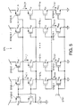
- FIG. 5 shows a detailed implementation of a preferred analog to digital converter 574.
- This preferred A/D converter accomplishes the whole processing in current mode. Alternatively, it can be implemented in voltage mode. It is a flash analog to digital converter. Its operation is based on the comparison of the filtered signal (represented in figure 5 by reference sign I scopy ) with several fixed current references I ref_1 I ref_2 ... I ref_N , so that when the current to be compared is smaller than the constant reference, the output voltage takes a low level and vice versa.
- I ref_N are selected as a function of the desired resolution to be obtained at the comparison of the corresponding currents and therefore as a function of the amount of bits which form part of the converter.
- the number N of current references can be chosen by the circuit designer. In a particular example, which should not be interpreted in a limiting way, 6 current references have been chosen I ref_1 I ref_2 I ref_3 I ref_4 I ref_5 I ref_6 . This number N of current references depends on the currents range managed by the limiter and by the desired accuracy.
- Currents I scopy are a copy of current I s ( figure 4 ), which flows through node V s ( figure 4 ) and is injected to transistors Msig 5742-1 5742-2... 5742-N (at node 5741 in figure 5 ). This way, N voltage values are obtained, depending on the number of references employed, which form an N-bit word.
- this circuit operates as follows: At node 5741, the output of the adder 473 is connected.
- the copy (I scopy ) of the current I s of the previous block 473 is mirrored at several branches through transistors M sig 5742-1 5742-2... 5742-N-1 5742-N and compared with scaled replicas of the fixed reference current I ref through transistors M ref 5743-0 5743-1 5743-2... 5743-N-1 5743-N.
- Transistors M cp and M cn are used in order to obtain current copies as exact as possible. If the signal value I s (or I scopy ) is higher than the reference current value I ref , the voltage of the output node b 1 b 2 ...
- b N-1 b N of the branch goes to ground GND. This can be considered as a low level (logic zero). If the signal value I s (I scopy ) is lower than the reference current I ref , the voltage of the output node b 1 b 2 ... b N-1 b N goes to a fixed value V DD and a logic one can be understood.
- the voltage values of the output nodes of every branch (b 1 b 2 ... b N-1 b N ) that form the A/D converter 574 give N bits that provide the received signal strength indicator signal. Note that the A/D converter 574 features low quiescent power consumption while involving simplicity and compactness.
- Non-limiting examples of such applications are: Bluetooth radio receiver, cellular radio devices, cordless telephones, wireless local area network radio devices or any other suitable radio devices.
- a received signal strength indicator has been described, which obtains a value of the power of a received signal in a different way from conventional RSSI circuits: While prior art RSSI circuits provide such value in absolute terms (either in natural or logarithmic form), the received signal strength indicator of the present invention provides a digital output (a digital code), from which the power level of the received signal can be deduced. In order to deduce such power level, knowledge of the relationship between that output digital code and the currents level managed by the limiter 160 (in turn dependent on the gain of the receiving chain) is required.
Landscapes
- Engineering & Computer Science (AREA)
- Quality & Reliability (AREA)
- Physics & Mathematics (AREA)
- Electromagnetism (AREA)
- Computer Networks & Wireless Communication (AREA)
- Signal Processing (AREA)
- Circuits Of Receivers In General (AREA)
Abstract
A received signal strength indicator (170, 270) for obtaining a received signal strength indicator signal (b1 b2... bN-1 bN) from an in-phase signal component (i(t)) and a quadrature signal component (q(t)), which comprises: first means for squaring (271, 371) an in-phase signal component (i(t)); second means for squaring (272, 372) a quadrature signal component (q(t)); adding means (273, 473) having a first input connected to the output (Io_I) of said first means for squaring (271, 371) and a second input connected to the output (Io_Q) of said second means for squaring (272, 372), for adding said first and second outputs (Io_I, Io_Q) of said respective first and second means for squaring (271, 371; 272, 372). It also comprises means for digitizing (274, 574) the output (Is) of said adding means (273, 473), said means for digitizing (274, 574) being configured for providing an output digital code (b1 b2... bN-1 bN) which represents a received signal strength indicator of a received signal.
Description
- The present invention relates to a received signal strength indicator circuit for a zero intermediate frequency radio device, such as a receiver or a transceiver.
- In wireless applications the received signal features a wide dynamic range. A magnitude control is thus required to keep the signal approximately constant and featuring enough signal-to-noise ratio (SNR) at the demodulator input for proper detection as well as for carrier sensing in Carrier Sense Multiple Access (CSMA) schemes. Moreover, low power consumption in a low voltage environment is mandatory for wireless design.
- A received signal strength indicator (RSSI) circuit is normally employed to represent the received signal strength. Depending on its value (strength), it can be used to adjust gain stages of different blocks and power down the receiver.
- A conventional RSSI for low-IF architectures is generally realized in logarithmic form as the wide dynamic variation of the received signal can be represented within a limited range. Also, a variable gain amplifier (VGA) is required to obtain the desired dynamic range. Successive detection architectures are adopted for the implementation of the logarithmic amplifier composed of several full-wave rectifiers and a low-pass filter.
- A possible solution to save power is to integrate these two functions into a single circuit, by sharing a single amplifier chain for both VGA and RSSI, as proposed by Chun-Pang Wu and Hen-Wai Tsao in "A 110-MHz 84-dB CMOS Programmable Gain Amplifier with Integrated RSSI Function", IEEE Journal of Solid-State Circuits, vol. 40, no. 6, June 2005).
- A similar approach is presented in US patent application
US-5338985-A , wherein a RSSI comprises cascaded amplifiers that amplify an intermediate frequency signal. These signals are rectified and after voltage to current conversion, currents are scaled and added. The resulting RSSI signal approximates a linear function of the logarithm of the input signal. - However, in a zero-IF receiver this kind of circuits cannot be used, as there are moments at which there is no presence of the carrier signal. At those moments detection fails.
- In US patent
US-6721548-B1 , a received signal strength indicator for operation at zero or low intermediate frequency and a related method are disclosed. It is based on several blocks: a hard limiter for calculating the absolute value of a signal; a block for summing the signals coming from the I-branch and Q-branch of the receiver; a block for obtaining the logarithmic value of the previous sum; a filter for low-pass filtering that logarithmic value; and for obtaining the strength value of the signal. In this disclosure, the obtained rssi signal is a concrete value, either expressed in natural units or in logarithmic units. - However, although the scheme disclosed in
US-6721548-B1 to obtain the received signal strength of the received signal works for zero intermediate frequency receivers, its implementation is not optimal. First of all, the blocks selected for the combination of signals in phase and quadrature are complex in terms of silicon area. Moreover, they do not make optimal use of the properties of the square law of metal-oxide-semiconductor transistors to calculate the amplitude of the combined signal (phase and quadrature). Finally, the complexity of the scheme drives to a solution that consumes more power than necessary for wireless application. - It is a primary aim of the present invention to provide a new scheme to implement a received signal strength indicator circuit that improves RSSI circuits of the state of the art.
- This is achieved by means of a received signal strength indicator circuit at zero intermediate frequency using a RSSI circuit with a simple topology and low power consumption. This low power consumption is obtained by means of an advantageous scheme used to obtain the RSSI signal using a flash A/D converter with very low quiescent power consumption. The signal obtained from the RSSI circuit of the invention can be used for controlling functions in the transceiver or to provide signal strength information to a system in which the transceiver operates.
- It is an object of the present invention to provide a received signal strength indicator for providing a received signal strength indicator signal from an in-phase signal component and a quadrature signal component, which comprises: first means for squaring an in-phase signal component; second means for squaring a quadrature signal component; adding means having a first input connected to the output of said first means for squaring and a second input connected to the output of said second means for squaring, for adding said first and second outputs of said respective first and second means for squaring. It also comprises means for digitizing the output of said adding means, said means for digitizing being configured for providing an output digital code which represents a received signal strength indicator of a received signal.
- Preferably, the adding means comprises a capacitor for filtering any ripple.
- Preferably, the means for digitizing is an analog to digital converter, and more preferably, a flash analog to digital converter.
- The A/D converter is preferably configured to work in current mode.
- The adding means preferably comprises a current mirror for copying a current corresponding to the added signal. In a preferred embodiment, that current mirror is a MOS cascode current mirror.
- In a preferred embodiment, the analog to digital converter comprises comparison means for comparing the copied current obtained at the adding means to a plurality of fixed, current references for obtaining a corresponding plurality of output voltage outputs which form the output digital code. Preferably, the comparison means comprises a plurality of transistors for mirroring said copied current and a plurality of transistors for comparing said fixed, current references to the copied current.
- Preferably, the first and second means for squaring operate with differential current inputs.
- The invention also provides a radio device which comprises a received signal strength indicator like the one previously mentioned. Preferably, the radio device is a zero intermediate frequency radio device.
- The advantages of the proposed invention will become apparent in the description that follows.
- To complete the description and in order to provide for a better understanding of the invention, a set of drawings is provided. Said drawings form an integral part of the description and illustrate a preferred embodiment of the invention, which should not be interpreted as restricting the scope of the invention, but rather as an example of how the invention can be embodied. The drawings comprise the following figures:
-
Figure 1 shows a block diagram of a receiver comprising a RSSI according to an embodiment of the present invention. -
Figure 2 shows a block diagram of a received signal strength indicator (RSSI) circuit according to an embodiment of the present invention. -
Figure 3 shows a block diagram of a squarer circuit according to an embodiment of the present invention. -
Figure 4 shows a block diagram of an adder and filtering scheme according to an embodiment of the present invention. -
Figure 5 shows a flash analog to digital converter according to an embodiment of the present invention. - In the context of the present invention, the terms "approximately", "about", "around", "almost", "near" and terms of its family (such as "approximate", etc.) should be understood as indicating values very near to those which accompany the aforementioned term. That is to say, a deviation within reasonable limits from an exact value should be accepted, because the expert in the technique will understand that such a deviation from the values indicated is inevitable due to measurement inaccuracies, etc.
- The implementation of the present invention can be carried out as follows:
-
Figure 1 shows a complete block diagram of a zerointermediate frequency receiver 100. Thereceiver 100 comprises an I-branch and a Q-branch. After a receiving antenna, a first filter is used. A low noise radio frequency amplifier (LNA) 110 drives a pair ofquadrature mixers 120, a first one located in a Q-branch and a second one located in an I-branch, the signal passing through the Q-branch being shifted 90° with respect to the signal passing through the I-branch. Each branch of the receiver chain is thus formed by the corresponding branch of thequadrature mixer 120. Thequadrature mixer 120 is preferably an active mixer in order to avoid preamplifier stages. Anotch filter 130 is used at each branch for eliminating the DC offset due to local oscillation (LO) leakage and mismatch. Next, two cascadedvoltage gain amplifiers 141 142 are used, followed by a lowpass channel filter 150. Next, alimiter 160 is cascaded at each of the branches. The outputs i(t) q(t) of theselimiters 160 are the inputs of aRSSI circuit 170. The outputs i(t) q(t) of thelimiters 160 are also the inputs of ademodulator 180, which in turn outputs the received data. -
Figure 2 shows a block diagram of a preferred embodiment of the received signal strength indicator (RSSI) 270. TheRSSI circuit 270 comprises twosquarer circuits 271 272, anadder 273 that includes a filtering function and an A/D converter 274. Preferably, the A/D converter 274 is a flash A/D converter.
As shown infigure 2 , theRSSI circuit 270 receives two currents: one is the in-phase component i(t) from the I-branch of thereceiver 100 and the other one is the quadrature component q(t) from the Q-branch of thereceiver 100. Each current is squared by asquarer block 271 272. Each squared current thus generated is summed up by anadder 273. Finally, the current obtained at theadder 273 is converted to a digital value by an analog todigital converter 274. As detailed later, the A/D converter 274 is implemented by a comparator scheme based on a reference current Iref. The output of thisblock 274 is the RSSI digital output which corresponds to the signal strength.
In this preferred embodiment, all the signal processing is made in current mode, although alternatively, voltage-mode implementations of the invention are also possible and can be devised straightforwardly.
Gains of several blocks of the receiver chain are controlled by the digital RSSI code. The received signal strength indicador (RSSI) 270 obtains, at its output, a group of digital bits ("1", "0"), also called a digital RSSI code. Depending on the output code, which indicates the strength of the received signal, and by means of certain logic, the gain of the receiver chain is controlled. -
Figure 3 shows a block diagram of any of the squarer circuits 371 372 offigure 2 . The squarer 371 372 is aimed at squaring (raising to the power of two) the incoming signal. This block 371 372 receives as inputs the differential output currents of thelimiters 160. Preferably, themultistage limiters 160 comprise a cascade of differential amplifiers. Usually, in squarer circuits, the outputs are the square of the input multiplied by a factor. In this particular embodiment, the output Io of each squarer 371 372 is given by: i2 /8·Ib where Ib is the bias current of this circuit. This particular implementation is based on the scheme proposed by Boonchai Boonchu and Wanlop Surakampontorn in "A CMOS current-mode squarer/rectifier circuit", ISCAS '03, which provides good benefits in terms of consumption. Any other squarer providing similar results could be used instead. If, alternatively to this current mode implementation, a voltage-mode implementation is chosen, the currents (i, Ib ) of the former expression are substituted by corresponding voltage ones (v, Vb ). -
Figure 4 shows adetailed implementation 473 of theadder circuit 273. It performs the sum of the squared signals Io_I Io_Q and filters, by means of acapacitor 4733, the ripple of the summed-up signal, caused by the high-pass notch filter 130 used for the elimination of DC offset. - It is well-known that one of the main problems in a zero IF receiver is the elimination of DC offset due to LO (Local Oscillator) leakage and mismatch. In order to solve this problem, an analog notch filter 130 (preferably comprising a first order RC high-pass filter) has been introduced in the receiver chain, as illustrated in
figure 1 . The presence of thisfilter 130 makes the in-phase and quadrature signals not be completely orthogonal, as the near-DC components of their spectrums are eliminated. This fact causes a considerable ripple after the output current signals are squared and added. Thecapacitor C f 4733 infigure 4 filters this ripple before converting the analog signal to a digital value. The value for thiscapacitor C f 4733 is selected depending on the bandwidth of a specific application. For example, for a Bluetooth application (around 1 MHz signal bandwidth) thiscapacitor C f 4733 takes a value equal to or near 10 pF. - The sum performed by the
adder 473 is made as follows: the outputs (which are, in this preferred embodiment, two currents Io_I Io_Q) coming from corresponding squarers 371 372 are injected at anode 4731. Acapacitor 4733 filters the ripple. The summed current IS flows into a MOS cascodecurrent mirror 4732. Preferably, this cascodecurrent mirror 4732 consists of a first transistor Mc and a second transistor Ms. Thisadder 473 is a conventional one. It is appreciated for its simplicity, but any other alternative adder could be used instead. As can be appreciated, thiscircuit 473 stands out for its simplicity due to the current mode signal processing and the absence of active blocks, such as operational amplifiers with feedback resistors. The purpose of the cascodecurrent mirror 4732 is to copy the IS current to the means for digitizing the output of theadder 473. This means for digitizing is preferably an A/D converter 274. -
Figure 5 shows a detailed implementation of a preferred analog todigital converter 574. This preferred A/D converter accomplishes the whole processing in current mode. Alternatively, it can be implemented in voltage mode. It is a flash analog to digital converter. Its operation is based on the comparison of the filtered signal (represented infigure 5 by reference sign Iscopy) with several fixed current references Iref_1 Iref_2... Iref_N, so that when the current to be compared is smaller than the constant reference, the output voltage takes a low level and vice versa. The values of the current references Iref_1 Iref_2... Iref_N are selected as a function of the desired resolution to be obtained at the comparison of the corresponding currents and therefore as a function of the amount of bits which form part of the converter. The number N of current references can be chosen by the circuit designer. In a particular example, which should not be interpreted in a limiting way, 6 current references have been chosen Iref_1 Iref_2 Iref_3 Iref_4 Iref_5 Iref_6. This number N of current references depends on the currents range managed by the limiter and by the desired accuracy. Currents Iscopy are a copy of current Is (figure 4 ), which flows through node Vs (figure 4 ) and is injected to transistors Msig 5742-1 5742-2... 5742-N (atnode 5741 infigure 5 ). This way, N voltage values are obtained, depending on the number of references employed, which form an N-bit word. - Basically, this circuit operates as follows: At
node 5741, the output of theadder 473 is connected. The copy (Iscopy) of the current Is of theprevious block 473 is mirrored at several branches through transistors Msig 5742-1 5742-2... 5742-N-1 5742-N and compared with scaled replicas of the fixed reference current Iref through transistors Mref 5743-0 5743-1 5743-2... 5743-N-1 5743-N. Transistors Mcp and Mcn are used in order to obtain current copies as exact as possible. If the signal value Is (or Iscopy) is higher than the reference current value Iref, the voltage of the output node b1 b2... bN-1 bN of the branch goes to ground GND. This can be considered as a low level (logic zero). If the signal value Is (Iscopy) is lower than the reference current Iref, the voltage of the output node b1 b2... bN-1 bN goes to a fixed value VDD and a logic one can be understood. The voltage values of the output nodes of every branch (b1 b2... bN-1 bN) that form the A/D converter 574 give N bits that provide the received signal strength indicator signal. Note that the A/D converter 574 features low quiescent power consumption while involving simplicity and compactness. This means that, once the comparison has been carried out, the consumption of all the branches with a voltage output near to the positive supply rail is almost zero, because through each of these branches of the A/D converter 574, reference current sources work in the cut-off region. Only the respective reference currents Iref_1 Iref_2 ... Iref_N of the branches with a voltage output near the negative supply rail flow from the positive to the negative supply rail, which is very low power consumption as these currents are scaled to be low valued. That is the reason why the quiescent power consumption is practically negligible. - These properties make this invention especially suitable for portable applications. Non-limiting examples of such applications are: Bluetooth radio receiver, cellular radio devices, cordless telephones, wireless local area network radio devices or any other suitable radio devices.
- A received signal strength indicator has been described, which obtains a value of the power of a received signal in a different way from conventional RSSI circuits: While prior art RSSI circuits provide such value in absolute terms (either in natural or logarithmic form), the received signal strength indicator of the present invention provides a digital output (a digital code), from which the power level of the received signal can be deduced. In order to deduce such power level, knowledge of the relationship between that output digital code and the currents level managed by the limiter 160 (in turn dependent on the gain of the receiving chain) is required.
- In this text, the term "comprises" and its derivations (such as "comprising", etc.) should not be understood in an excluding sense, that is, these terms should not be interpreted as excluding the possibility that what is described and defined may include further elements, steps, etc.
- The invention is obviously not limited to the specific embodiments described herein, but also encompasses any variations that may be considered by any person skilled in the art (for example, as regards the choice of components, configuration, etc.), within the general scope of the invention as defined in the appended claims.
Claims (12)
- A received signal strength indicator (170, 270) for providing a received signal strength indicator signal (b1 b2... bN-1 bN) from an in-phase signal component (i(t)) and a quadrature signal component (q(t)), which comprises:- first means for squaring (271, 371) an in-phase signal component (i(t));- second means for squaring (272, 372) a quadrature signal component (q(t));- adding means (273, 473) having a first input connected to the output (Io_I) of said first means for squaring (271, 371) and a second input connected to the output (Io_Q) of said second means for squaring (272, 372), for adding said first and second outputs (Io_I, Io_Q) of said respective first and second means for squaring (271, 371; 272, 372);characterised in that it further comprises means for digitizing (274, 574) the output (Is) of said adding means (273, 473), said means for digitizing (274, 574) being configured for providing an output digital code (b1 b2... bN-1 bN) which represents a received signal strength indicator of a received signal.
- The received signal strength indicator (170, 270) of claim 1, wherein said adding means (273, 473) comprises a capacitor (4733) for filtering any ripple.
- The received signal strength indicator (170, 270) of either claim 1 or 2, wherein said means for digitizing (274, 574) is an analog to digital converter (274, 574).
- The received signal strength indicator (170, 270) of claim 3, wherein said analog to digital converter (274, 574) is a flash analog to digital converter (274, 574).
- The received signal strength indicator (170, 270) of either claim 3 or 4, wherein said A/D converter is configured to work in current mode.
- The received signal strength indicator (170, 270) of claim 5, wherein said adding means (273, 473) comprises a current mirror (4732) for copying (Iscopy) a current (Is) corresponding to the added signal.
- The received signal strength indicator (170, 270) of claim 6, wherein said current mirror (4732) is a MOS cascode current mirror.
- The received signal strength indicator (170, 270) of either claim 6 or 7, wherein said analog to digital converter (574) comprises comparison means for comparing the copied current (Iscopy) obtained at the adding means (273, 473) to a plurality of fixed, current references (Iref_1, Iref_2,... Iref_N) for obtaining a corresponding plurality of output voltage outputs which form said output digital code (b1 b2... bN-1 bN).
- The received signal strength indicator (170, 270) of claim 8, wherein said comparison means comprises a plurality of transistors (5742-1 5742-2... 5742-N-1 5742-N) for mirroring said copied current (Iscopy) and a plurality of transistors (5743-0 5743-1 5743-2... 5743-N-1 5743-N) for comparing said fixed, current references (Iref_1, Iref_2,... Iref_N) to said copied current (Iscopy).
- The received signal strength indicator (170, 270) of any preceding claim, wherein said first and second means for squaring (271, 371; 272, 372) operate with differential current inputs.
- A radio device (100) which comprises a received signal strength indicator (170, 270) according to any preceding claim.
- The radio device (100) of claim 11, which is a zero intermediate frequency radio device.
Priority Applications (1)
| Application Number | Priority Date | Filing Date | Title |
|---|---|---|---|
| EP08164237A EP2164191A1 (en) | 2008-09-12 | 2008-09-12 | Low power received signal strength indicator |
Applications Claiming Priority (1)
| Application Number | Priority Date | Filing Date | Title |
|---|---|---|---|
| EP08164237A EP2164191A1 (en) | 2008-09-12 | 2008-09-12 | Low power received signal strength indicator |
Publications (1)
| Publication Number | Publication Date |
|---|---|
| EP2164191A1 true EP2164191A1 (en) | 2010-03-17 |
Family
ID=40364420
Family Applications (1)
| Application Number | Title | Priority Date | Filing Date |
|---|---|---|---|
| EP08164237A Withdrawn EP2164191A1 (en) | 2008-09-12 | 2008-09-12 | Low power received signal strength indicator |
Country Status (1)
| Country | Link |
|---|---|
| EP (1) | EP2164191A1 (en) |
Cited By (1)
| Publication number | Priority date | Publication date | Assignee | Title |
|---|---|---|---|---|
| TWI699109B (en) * | 2018-12-26 | 2020-07-11 | 全一電子股份有限公司 | Wireless signal level indicator |
Citations (4)
| Publication number | Priority date | Publication date | Assignee | Title |
|---|---|---|---|---|
| US5338985A (en) | 1991-06-03 | 1994-08-16 | North American Philips Corporation | Low voltage, simplified and temperature compensated logarithmic detector |
| DE19954348A1 (en) * | 1998-11-11 | 2000-05-18 | Advantest Corp | Electrical power measuring system for radio communications device, uses digital filter network for simultaneous frequency band limitation and signal mixing |
| WO2001047154A1 (en) * | 1999-12-22 | 2001-06-28 | Koninklijke Philips Electronics N.V. | High dynamic range low ripple rssi for zero-if or low-if receivers |
| WO2004062142A1 (en) * | 2003-01-07 | 2004-07-22 | Philips Intellectual Property & Standards Gmbh | Method and circuit arrangement for determining the signal strength in receivers with complex signal processing |
-
2008
- 2008-09-12 EP EP08164237A patent/EP2164191A1/en not_active Withdrawn
Patent Citations (5)
| Publication number | Priority date | Publication date | Assignee | Title |
|---|---|---|---|---|
| US5338985A (en) | 1991-06-03 | 1994-08-16 | North American Philips Corporation | Low voltage, simplified and temperature compensated logarithmic detector |
| DE19954348A1 (en) * | 1998-11-11 | 2000-05-18 | Advantest Corp | Electrical power measuring system for radio communications device, uses digital filter network for simultaneous frequency band limitation and signal mixing |
| WO2001047154A1 (en) * | 1999-12-22 | 2001-06-28 | Koninklijke Philips Electronics N.V. | High dynamic range low ripple rssi for zero-if or low-if receivers |
| US6721548B1 (en) | 1999-12-22 | 2004-04-13 | Koninklijke Philips Electronics N.V. | High dynamic range low ripple RSSI for zero-IF or low-IF receivers |
| WO2004062142A1 (en) * | 2003-01-07 | 2004-07-22 | Philips Intellectual Property & Standards Gmbh | Method and circuit arrangement for determining the signal strength in receivers with complex signal processing |
Non-Patent Citations (1)
| Title |
|---|
| CHUN-PANG WU; HEN-WAI TSAO: "A 110-MHz 84-dB CMOS Programmable Gain Amplifier with Integrated RSSI Function", IEEE JOURNAL OF SOLID-STATE CIRCUITS, vol. 40, no. 6, June 2005 (2005-06-01), XP011133172, DOI: doi:10.1109/JSSC.2005.848023 |
Cited By (1)
| Publication number | Priority date | Publication date | Assignee | Title |
|---|---|---|---|---|
| TWI699109B (en) * | 2018-12-26 | 2020-07-11 | 全一電子股份有限公司 | Wireless signal level indicator |
Similar Documents
| Publication | Publication Date | Title |
|---|---|---|
| US7184737B2 (en) | Image-rejection I/Q demodulators | |
| US8717077B2 (en) | Duty cycle adjustment for a local oscillator signal | |
| US7116948B2 (en) | High-speed signal power detection circuit | |
| US7116259B2 (en) | Switching between lower and higher power modes in an ADC for lower/higher precision operations | |
| EP3149849B1 (en) | Transmitter digital-to-analog converter (dac)- baseband filter (bbf) common mode interface | |
| US7974376B2 (en) | High precision continuous time gmC BPF tuning | |
| CN102624412A (en) | Semiconductor integrated circuit and operation method of the same | |
| US20060092061A1 (en) | Continuous-time delta-sigma ADC with programmable input range | |
| Byun et al. | A low-power CMOS Bluetooth RF transceiver with a digital offset canceling DLL-based GFSK demodulator | |
| KR101009077B1 (en) | Apparatus and method for DC offset compensation in direct conversion receiver | |
| US7324037B1 (en) | Analog to digital converter with interference rejection capability | |
| US20050250459A1 (en) | Compensation of a DC offset in a receiver | |
| US7522891B2 (en) | High frequency peak power detection circuit | |
| US7936298B2 (en) | Integrated circuit and electronic device comprising threshold generation circuitry and method therefor | |
| US9037106B2 (en) | Baseband harmonic rejection circuit | |
| US20120019314A1 (en) | Current-mode analog baseband apparatus | |
| KR20060076300A (en) | Mixer circuit, receiver for receiving radio frequency signal, method of generating output signal by mixing input signal with oscillator signal | |
| EP2164191A1 (en) | Low power received signal strength indicator | |
| US7167692B2 (en) | High frequency peak detector and applications thereof | |
| US8787503B2 (en) | Frequency mixer with compensated DC offset correction to reduce linearity degradation | |
| US9525447B1 (en) | Radio receiver co-existence | |
| KR20040014059A (en) | High speed digital RSSI circuit | |
| Chen et al. | Searching for spectrum holes: A 400–800 MHz spectrum sensing system | |
| Ken et al. | An automatic DC-Offset cancellation method and circuit for RF transceivers | |
| CN103312647A (en) | Fine RF transceiver dc offset calibration method |
Legal Events
| Date | Code | Title | Description |
|---|---|---|---|
| PUAI | Public reference made under article 153(3) epc to a published international application that has entered the european phase |
Free format text: ORIGINAL CODE: 0009012 |
|
| AK | Designated contracting states |
Kind code of ref document: A1 Designated state(s): AT BE BG CH CY CZ DE DK EE ES FI FR GB GR HR HU IE IS IT LI LT LU LV MC MT NL NO PL PT RO SE SI SK TR |
|
| AX | Request for extension of the european patent |
Extension state: AL BA MK RS |
|
| AKY | No designation fees paid | ||
| REG | Reference to a national code |
Ref country code: DE Ref legal event code: 8566 |
|
| STAA | Information on the status of an ep patent application or granted ep patent |
Free format text: STATUS: THE APPLICATION IS DEEMED TO BE WITHDRAWN |
|
| 18D | Application deemed to be withdrawn |
Effective date: 20101001 |