EP2164094A1 - A method for reducing fermi-level-pinning in a non-silicon channel mos device - Google Patents
A method for reducing fermi-level-pinning in a non-silicon channel mos device Download PDFInfo
- Publication number
- EP2164094A1 EP2164094A1 EP09075423A EP09075423A EP2164094A1 EP 2164094 A1 EP2164094 A1 EP 2164094A1 EP 09075423 A EP09075423 A EP 09075423A EP 09075423 A EP09075423 A EP 09075423A EP 2164094 A1 EP2164094 A1 EP 2164094A1
- Authority
- EP
- European Patent Office
- Prior art keywords
- high mobility
- compound
- iii
- semiconductor
- gate dielectric
- Prior art date
- Legal status (The legal status is an assumption and is not a legal conclusion. Google has not performed a legal analysis and makes no representation as to the accuracy of the status listed.)
- Granted
Links
Images








Classifications
-
- H—ELECTRICITY
- H10—SEMICONDUCTOR DEVICES; ELECTRIC SOLID-STATE DEVICES NOT OTHERWISE PROVIDED FOR
- H10P—GENERIC PROCESSES OR APPARATUS FOR THE MANUFACTURE OR TREATMENT OF DEVICES COVERED BY CLASS H10
- H10P95/00—Generic processes or apparatus for manufacture or treatments not covered by the other groups of this subclass
- H10P95/94—Hydrogenation or deuterisation, e.g. using atomic hydrogen from a plasma
-
- H—ELECTRICITY
- H10—SEMICONDUCTOR DEVICES; ELECTRIC SOLID-STATE DEVICES NOT OTHERWISE PROVIDED FOR
- H10D—INORGANIC ELECTRIC SEMICONDUCTOR DEVICES
- H10D30/00—Field-effect transistors [FET]
- H10D30/60—Insulated-gate field-effect transistors [IGFET]
-
- H—ELECTRICITY
- H10—SEMICONDUCTOR DEVICES; ELECTRIC SOLID-STATE DEVICES NOT OTHERWISE PROVIDED FOR
- H10D—INORGANIC ELECTRIC SEMICONDUCTOR DEVICES
- H10D30/00—Field-effect transistors [FET]
- H10D30/60—Insulated-gate field-effect transistors [IGFET]
- H10D30/751—Insulated-gate field-effect transistors [IGFET] having composition variations in the channel regions
-
- H—ELECTRICITY
- H10—SEMICONDUCTOR DEVICES; ELECTRIC SOLID-STATE DEVICES NOT OTHERWISE PROVIDED FOR
- H10D—INORGANIC ELECTRIC SEMICONDUCTOR DEVICES
- H10D64/00—Electrodes of devices having potential barriers
- H10D64/01—Manufacture or treatment
- H10D64/013—Manufacture or treatment of electrodes having a conductor capacitively coupled to a semiconductor by an insulator
- H10D64/01302—Manufacture or treatment of electrodes having a conductor capacitively coupled to a semiconductor by an insulator the insulator being formed after the semiconductor body, the semiconductor being silicon
- H10D64/01332—Making the insulator
- H10D64/01336—Making the insulator on single crystalline silicon, e.g. chemical oxidation using a liquid
- H10D64/01338—Making the insulator on single crystalline silicon, e.g. chemical oxidation using a liquid with a treatment, e.g. annealing, after the formation of the conductor
-
- H—ELECTRICITY
- H10—SEMICONDUCTOR DEVICES; ELECTRIC SOLID-STATE DEVICES NOT OTHERWISE PROVIDED FOR
- H10D—INORGANIC ELECTRIC SEMICONDUCTOR DEVICES
- H10D64/00—Electrodes of devices having potential barriers
- H10D64/01—Manufacture or treatment
- H10D64/013—Manufacture or treatment of electrodes having a conductor capacitively coupled to a semiconductor by an insulator
- H10D64/01302—Manufacture or treatment of electrodes having a conductor capacitively coupled to a semiconductor by an insulator the insulator being formed after the semiconductor body, the semiconductor being silicon
- H10D64/01332—Making the insulator
- H10D64/01336—Making the insulator on single crystalline silicon, e.g. chemical oxidation using a liquid
- H10D64/0134—Making the insulator on single crystalline silicon, e.g. chemical oxidation using a liquid with a treatment, e.g. annealing, after the formation of the insulator and before the formation of the conductor
-
- H—ELECTRICITY
- H10—SEMICONDUCTOR DEVICES; ELECTRIC SOLID-STATE DEVICES NOT OTHERWISE PROVIDED FOR
- H10D—INORGANIC ELECTRIC SEMICONDUCTOR DEVICES
- H10D64/00—Electrodes of devices having potential barriers
- H10D64/01—Manufacture or treatment
- H10D64/013—Manufacture or treatment of electrodes having a conductor capacitively coupled to a semiconductor by an insulator
- H10D64/01302—Manufacture or treatment of electrodes having a conductor capacitively coupled to a semiconductor by an insulator the insulator being formed after the semiconductor body, the semiconductor being silicon
- H10D64/01332—Making the insulator
- H10D64/01336—Making the insulator on single crystalline silicon, e.g. chemical oxidation using a liquid
- H10D64/01342—Making the insulator on single crystalline silicon, e.g. chemical oxidation using a liquid by deposition, e.g. evaporation, ALD or laser deposition
-
- H—ELECTRICITY
- H10—SEMICONDUCTOR DEVICES; ELECTRIC SOLID-STATE DEVICES NOT OTHERWISE PROVIDED FOR
- H10D—INORGANIC ELECTRIC SEMICONDUCTOR DEVICES
- H10D64/00—Electrodes of devices having potential barriers
- H10D64/01—Manufacture or treatment
- H10D64/013—Manufacture or treatment of electrodes having a conductor capacitively coupled to a semiconductor by an insulator
- H10D64/01356—Manufacture or treatment of electrodes having a conductor capacitively coupled to a semiconductor by an insulator the insulator being formed after the semiconductor body, the semiconductor being a Group IV material and not being silicon, e.g. Ge, SiGe or SiGeC
-
- H—ELECTRICITY
- H10—SEMICONDUCTOR DEVICES; ELECTRIC SOLID-STATE DEVICES NOT OTHERWISE PROVIDED FOR
- H10D—INORGANIC ELECTRIC SEMICONDUCTOR DEVICES
- H10D64/00—Electrodes of devices having potential barriers
- H10D64/01—Manufacture or treatment
- H10D64/013—Manufacture or treatment of electrodes having a conductor capacitively coupled to a semiconductor by an insulator
- H10D64/01358—Manufacture or treatment of electrodes having a conductor capacitively coupled to a semiconductor by an insulator the insulator being formed after the semiconductor body, the semiconductor being a Group III-V material
-
- H—ELECTRICITY
- H10—SEMICONDUCTOR DEVICES; ELECTRIC SOLID-STATE DEVICES NOT OTHERWISE PROVIDED FOR
- H10D—INORGANIC ELECTRIC SEMICONDUCTOR DEVICES
- H10D64/00—Electrodes of devices having potential barriers
- H10D64/60—Electrodes characterised by their materials
- H10D64/66—Electrodes having a conductor capacitively coupled to a semiconductor by an insulator, e.g. MIS electrodes
- H10D64/68—Electrodes having a conductor capacitively coupled to a semiconductor by an insulator, e.g. MIS electrodes characterised by the insulator, e.g. by the gate insulator
- H10D64/691—Electrodes having a conductor capacitively coupled to a semiconductor by an insulator, e.g. MIS electrodes characterised by the insulator, e.g. by the gate insulator comprising metallic compounds, e.g. metal oxides or metal silicates
-
- H—ELECTRICITY
- H10—SEMICONDUCTOR DEVICES; ELECTRIC SOLID-STATE DEVICES NOT OTHERWISE PROVIDED FOR
- H10P—GENERIC PROCESSES OR APPARATUS FOR THE MANUFACTURE OR TREATMENT OF DEVICES COVERED BY CLASS H10
- H10P95/00—Generic processes or apparatus for manufacture or treatments not covered by the other groups of this subclass
- H10P95/90—Thermal treatments, e.g. annealing or sintering
Definitions
- the present invention relates to the use of high mobility materials such as Ge and III-V compounds (e.g. GaAs or InGaAs) as a channel in a Metal Oxide Semiconductor (MOS) device thereby replacing silicon.
- high mobility materials such as Ge and III-V compounds (e.g. GaAs or InGaAs) as a channel in a Metal Oxide Semiconductor (MOS) device thereby replacing silicon.
- MOS Metal Oxide Semiconductor
- the present invention relates to a method for reducing (avoiding) Fermi Level Pinning (FLP) in high mobility materials such as in a Ge or III-V semiconductor compound based channel in a MOS device.
- FLP Fermi Level Pinning
- the present invention further relates to passivation methods which reduces drastically (avoiding) FLP.
- CMOS Complementary Metal Oxide Semiconductor
- MOSFET Metal Oxide Semiconductor Field effect transistor
- Germanium and III-V compounds such as InSb, InAs, Ge and InGaAs with high electron mobility are very promising materials and possible solutions for CMOS devices beyond 22nm.
- IPL interfacial passivation layer
- EOT ⁇ 0.8 nm at 16 nm node
- the diffusion of Si or Ge into III-V substrate under high temperature process such as implant activation anneals (>650C) can alter the substrate doping significantly.
- the application of more than several nanometers of IPL material Si or Ge, with 400cm 2 /eV and 1900cm 2 /eV electron mobility respectively
- will likely degrade the high carrier mobility of the substrate (8000cm 2 /eV for In 0.53 Ga 0.47 As).
- the present invention aims to reduce Fermi Level Pinning (FLP) in a high mobility material such as a Ge (SiGe) or III-V semiconductor compound based channel in a MOS device.
- FLP Fermi Level Pinning
- the present invention aims to reduce FLP and in the mean time to enhance the device characteristics significantly.
- the present invention furthermore aims to integrate InGaAs/Ge for high performance MOS devices with an emphasis on progressive EOT (Equivalent Oxide Thickness) scaling.
- the present invention relates to a method for avoiding or at least reducing drastically the Fermi Level Pinning (FLP) effects in new channel materials with higher carrier mobility such as a Ge or III-V compound based channel of a MOS device and thereby improving the device performance drastically.
- FLP Fermi Level Pinning
- new channel materials with higher carrier mobility such as a Ge or III-V compound based channel of a MOS device
- said Fermi Level Pinning (FLP) effects are arising from the very high interfacial trap density at the Ge (SiGe) or III-V compound semiconductor interface with the gate dielectric situated above said compound semiconductor.
- HFIL high frequency inversion lift
- a method is disclosed to fabricate a device having a channel made of a Ge (SiGe) or III/V semiconductor compound high mobility material thereby avoiding the problem of FLP.
- said device is a MOS device comprising a Ge (SiGe) or alternatively a III-V compound based channel or in other words a device utilizing high mobility Ge (SiGe) or III-V materials (such as GaAs or InGaAs) as the channel material and thereby replacing conventionally used silicon based channels.
- the method avoids the use (deposition) of an interfacial passivation layer (IPL) (e.g., Si or Ge) in between the high mobility III-V compound semiconductor and the gate dielectric layer.
- IPL interfacial passivation layer
- the method of the preferred embodiments uses a passivation technique which can not only reduce (eliminate) the FLP but also can enhance the device characteristics significantly.
- the method of preferred embodiments solves the problem of FLP by passivating the high mobility material at the interface of the gate dielectric and the Ge or III-V compound semiconductor and at the same time repairing the defects at said interface.
- the problem is solved by performing an atomic hydrogen anneal or a forming gas anneal in the form of a Catalytic Forming Gas Anneal (C-FGA) in order to achieve atomic hydrogen.
- Said atomic hydrogen anneal is preferably a non-damaging plasma hydrogen anneal such as the use of a remote plasma.
- Said C-FGA is preferably a FGA performed in the presence of certain noble metals such as Pt or Pd which transforms molecular hydrogen into atomic hydrogen.
- the atomic hydrogen anneal step is preferably performed before depositing the gate electrode. Alternatively said atomic hydrogen anneal step is performed after depositing the gate electrode or in other words after creation of the MOS structure.
- a method for reducing (avoiding) Fermi Level Pinning in a germanium (Ge, SiGe) or III-V high mobility compound channel of a metal oxide semiconductor (MOS) device comprising at least the steps of:
- said MOS device may be a MOSCAP, MOSFET, HEMT,... including a high mobility Ge (SiGe) or III-V compound semiconductor based channel which can be a surface channel or a buried channel.
- MOSCAP MOSCAP
- MOSFET MOSFET
- HEMT HEMT
- III-V compound semiconductor based channel which can be a surface channel or a buried channel.
- said MOS device is a MOSFET including a high mobility Ge (SiGe) or III-V compound based channel and the method for reducing (avoiding) the FLP effect in said MOSFET comprises at least the steps of:
- the substrate is chosen such that a dislocation free growth of the high mobility compound semiconductor onto the substrate is possible.
- the substrate may be made of Si (e.g. a Si wafer), InP, or the like.
- the III-V compound semiconductor is InGaAs, preferably In x Ga 1-x As with x>0.5 and more preferably In 0.53 Ga 0.47 As.
- the III-V compound semiconductor is preferably lattice matched towards the underlying substrate, e.g. In 0.53 Ga 0.47 As can be grown lattice matched onto a Si substrate using state of the art techniques.
- the compound semiconductor is Ge or Si x Ge 1-x with x ⁇ 0.3.
- the Ge compound semiconductor is preferably deposited dislocation free onto the underlying substrate.
- Said substrate may be made of Si, Ge, or the like.
- said Ge or Si x Ge 1-x is being annealed to achieve a GeOx (most preferably GeO 2 top surface layer.
- the grown Ge (SiGe) compound semiconductor or III-V compound semiconductor e.g. In 0.53 Ga 0.47 As further undergoes a chalcogenide passivation process in order to remove the native oxides.
- the compound semiconductor is Ge
- the formation of a GeOx (most preferably GeO 2 top surface layer is avoided (not needed).
- the method further includes the step of dipping the substrate in a solution of 40-48% wt%, (NH 4 ) 2 S for 5 to 10 minutes and rinse to dry with de-ionized water.
- H 2 S (gas) treatments may be used to perform the chalcogenide passivation.
- the chalcogenide passivation step is performed before the step of forming a gate dielectric 17 on the Ge (SiGe) or III-V compound semiconductor.
- the step of forming a gate dielectric onto the Ge (SiGe)or III-V compound semiconductor comprises depositing an oxide selected from a group consisting of Al 2 O 3 , HfO 2 , ZrO 2 , Ga 2 O 3 , Gd 2 O 3 , Y 2 O 3 , TiO 2 , Ta 2 O 5 , La 2 O 3 , HfAlO, TiAlO, and La x Al 1-x O 3 (LaAlO 3 )
- the step of forming a gate dielectric layer onto the Ge (SiGe) or III-V compound semiconductor comprises depositing a layer of Al 2 O 3 through atomic layer deposition (ALD) or alternatively Molecular Beam Epitaxy (MBE).
- ALD atomic layer deposition
- MBE Molecular Beam Epitaxy
- the thickness of the deposited gate dielectric may be in the range of 5nm up to 20nm to fabricate a MOSCAP device and within an EOT thickness ⁇ 1nm to fabricate a MOSFET device.
- the step of providing a gate electrode onto the gate dielectric is performed using deposition techniques such as Physical Vapor Deposition (PVD), e-beam evaporation and RF sputtering, or the like.
- the thickness of the deposited gate electrode structure may be in the range of 50nm up to 200nm.
- the gate electrode (metal) layer is subsequently patterned to form a gate electrode structure using state of the art patterning techniques to achieve the suitable gate structure.
- the step of performing the hydrogen anneal is performed using atomic hydrogen anneal e.g. using a remote plasma with 10%-100% atomic hydrogen in an inert carrier gas, preferably at a temperature in the range of 200oC up to 500oC, more preferred in the range of 300 o C up to 500oC for about at least 5 up to 30 minutes.
- This method is non-destructive compared to state of the art techniques used to passivate the Ge (SiGe) or III-V compound semiconductor e.g. using a plasma treatment involving energy bombardment.
- the step of performing the hydrogen anneal is performed using C-FGA in combination with noble metals such as Pt and Pd, whereby said noble metals are acting as a catalyst to dissociate molecular hydrogen into atomic hydrogen.
- Said C-FGA is preferably performed at a temperature in the range of 200oC up to 500oC, more preferred in the range of 300 oC up to 500oC for about at least 5 up to 30 minutes.
- the step of performing the hydrogen anneal is performed using C-FGA which is performed after depositing a gate electrode onto said gate dielectric and wherein said gate electrode is comprising a noble metal such as Pt or Pd which transforms molecular hydrogen into atomic hydrogen.
- the step of performing the atomic hydrogen anneal is performed using deuterium (e.g. 10%-100%), preferably at a temperature in the range of 200oC up to 500oC, more preferred between 300oC up to 400oC for about at least 5 up to 30 minutes.
- deuterium e.g. 10%-100%
- a method is disclosed of forming a MOS device including a high mobility Ge (SiGe)or III-V compound semiconductor based channel whereby a field-induced surface quantum well is created at the interface between the Ge (SiGe)or III-V compound and the gate dielectric.
- a high frequency inversion lift (HFIL) is observed on the CV curve because the channel interface has a very low defectivity and high mobility.
- the obtained high mobility MOS device has a high frequency inversion lifting (HFIL) in the range of 10% up to 20%.
- a MOS device comprising a high mobility III-V semiconductor compound based channel wherein a (surface) quantum well is created and observed at the gate dielectric - semiconductor compound based channel interface.
- Said device comprises at least:
- said MOS device comprising a high mobility In x Ga 1-x As (preferably In 0.53 Ga 0.47 As) semiconductor compound based channel having a (surface) quantum well further comprises a first and second region within the In x Ga 1-x As semiconductor compound which is doped with an n-type dopant to form a source and drain of the MOS device and an In x Ga 1-x As semiconductor compound channel which is being doped with a p-type dopant to form an N-MOS device with a (surface) quantum well.
- a high mobility In x Ga 1-x As (preferably In 0.53 Ga 0.47 As) semiconductor compound based channel having a (surface) quantum well further comprises a first and second region within the In x Ga 1-x As semiconductor compound which is doped with an n-type dopant to form a source and drain of the MOS device and an In x Ga 1-x As semiconductor compound channel which is being doped with a p-type dopant to form an N-MOS device with a (surface) quantum well.
- a MOS device comprising a high mobility Ge (SiGe) semiconductor compound based channel wherein a (surface) quantum well is created and observed at the gate oxide - semiconductor compound based channel interface.
- Said device preferably comprises:
- said MOS device comprising a high mobility Ge (SiGe) semiconductor compound based channel having a (surface) quantum well further comprises a first and second region within the Ge (SiGe) semiconductor compound which is doped with a p-type dopant to form a source and drain of a MOS device and a Ge (SiGe) semiconductor compound channel which is being doped with an n-type dopant to form a P-MOS device.
- a high mobility CMOS device comprising a high mobility P-MOSFET and a high mobility N-MOSFET.
- Said CMOS device is preferably comprising a Ge (SiGe) semiconductor compound P-MOSFET wherein the source and drain regions are doped with a p-type dopant.
- Said CMOS device is preferably further comprising a In x Ga 1-x As (preferably In 0.53 Ga 0.47 As) semiconductor compound N-MOSFET wherein the source and drain regions are doped with an n-type dopant.
- a field-induced surface quantum well is achieved within the high mobility MOS device by passivating the interface between the gate oxide and the semiconductor compound.
- Said passivation is performed using the method of the preferred embodiments making use of an anneal process with atomic hydrogen.
- Said hydrogen anneal may be C-FGA (molecular hydrogen) in combination with a noble metal, alternatively atomic hydrogen may be used.
- the hydrogen anneal may be performed before or after the step of depositing the gate electrode.
- Figure 1 illustrates a suitable MOS capacitor stacks according to preferred embodiments.
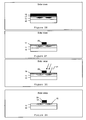
- FIGS 2A-2H illustrate the process flow according to preferred embodiments of invention to fabricate a metal oxide semiconductor field-effect transistor (MOSFET) including a high mobility Ge or III-V compound based channel thereby avoiding (eliminating) the FLP effect.
- MOSFET metal oxide semiconductor field-effect transistor
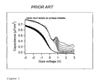
- FIG. 3 illustrates the capacitance-voltage (C-V) curve for a MOS capacitor sample having a 10nm Al 2 O 3 /p-type doped In 0.53 Ga 0.47 As stack without the atomic hydrogen anneal (FGA) treatment (PRIOR ART).
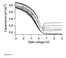
- Figure 4 illustrates the capacitance-voltage (C-V) curve for a MOS capacitor sample having a 10nm Al 2 O 3 /p-type doped In 0.53 Ga 0.47 As stack with a Pd gate on top of it after hydrogen anneal (C-FGA) according to preferred embodiments of the preferred embodiments of the invention.
- the HFIL is indicated in Figure 4 .
- Figure 5 illustrates the CV curve of a device having an 8 nm Al 2 O 3 /p-type doped In 0.53 Ga 0.47 As stack according to conventional capacitance/voltage characteristic interpretations without taking the adaptations according to Martens et al. into account.
- Figure 6 illustrates a CV curve according to preferred embodiments of the invention for an In 0.53 Ga 0.47 As MOS capacitor illustrating true inversion response and having a bias independent characteristic at inversion.
- the MOS capacitor was measured from 1KHz to 1MHz, with a total of 30 frequencies.
- Figure 7 illustrates the MOSFET Inversion circuit model (PRIOR ART).
- the resistive element R models the 'communication path' between the majority carrier band and the minority carrier band.
- Figures 8A-8B illustrate gate dielectric (oxide)-InGaAs field-induced surface quantum well formation in a III/V MOS capacitor comprising MOSFET stack according to preferred embodiments of invention.
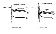
- Figures 9A-9B illustrate Ge field-induced surface quantum well formation in a high mobility Ge MOS capacitor stack according to preferred embodiments of invention.
- Figure 9A illustrates the behaviour at 1MHz without performing the C-FGA;
- Figure 9B illustrates the behaviour at 1MHz after performing the C-FGA according to preferred embodiments of the preferred embodiments thereby illustrating a true inversion at 1MHz and formation of a field-induced surface quantum well.
- Figure 10 illustrates a CV curve for a Ge MOS capacitor.
- Figure 10A illustrates the CV curve for a Ge MOS capacitor without performing a C-FGA and
- Figure 10B illustrates the CV curve for a Ge MOS capacitor after performing the C-FGA according to preferred embodiments of the preferred embodiments showing a true inversion response and a bias independent characteristic at inversion.
- the MOS capacitor was measured from 1KHz to 1MHz, with a total of 30 frequencies.
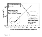
- Figure 11 illustrates D it distributions of the Ge and InGaAs MOSCAPs according to preferred embodiments of invention.
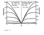
- Figure 12 illustrates Id-Vd plots of a 1.5 ⁇ m Ge P-MOSFET and InGaAs N-MOSFET according to preferred embodiments of invention.
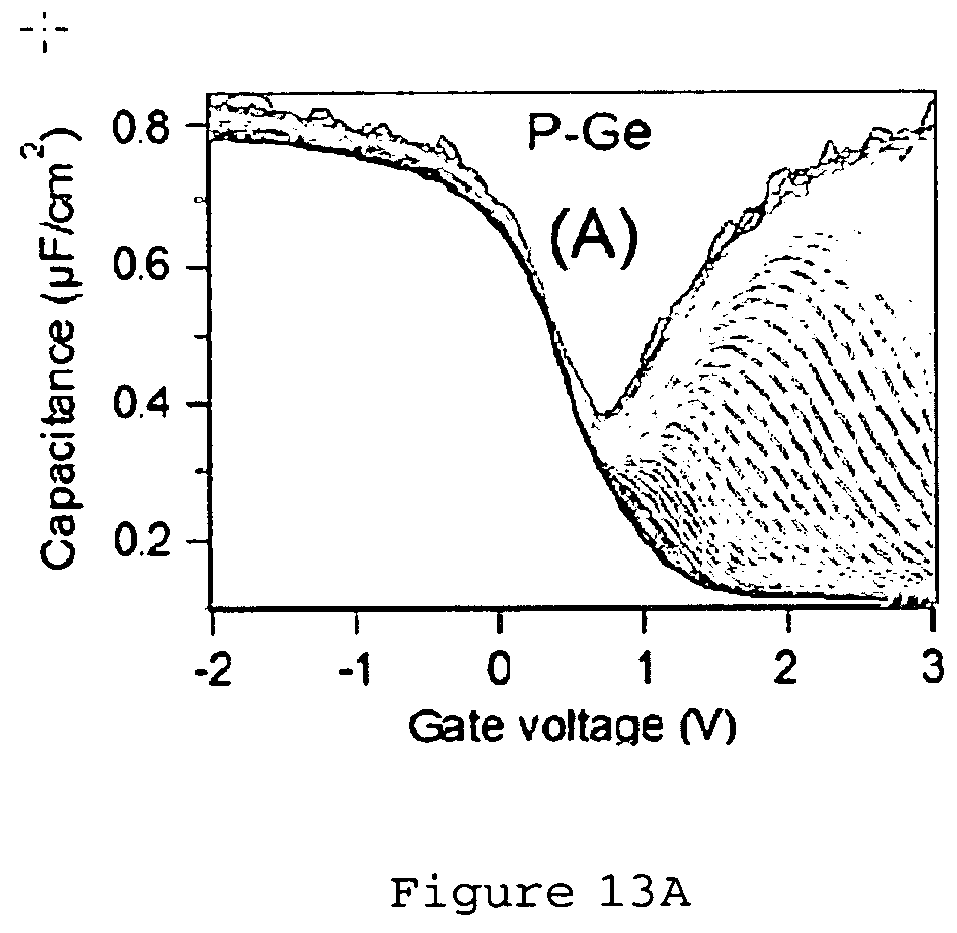
- Figure 13 illustrates C-V curves of Ge and InGaAs MOSCAPs according to preferred embodiments of invention.
- Figure 13 illustrates a p-type Ge MOSCAP ( Figure 13A ), a n-type Ge MOSCAP ( Figure 13B ), an InGaAs n-type MOSCAP ( Figure 13C ) and an InGaAs n-type MOSCAP ( Figure 13D ).
- EOT Equivalent Oxide Thickness
- HFIL High frequency inversion lift
- HFIL is the phenomenon in which the CV reveals a step up (lift) at the strong inversion even at high frequency.
- the HFIL 0 at about 100 Hz.
- C-FGA the method of the preferred embodiments (after C-FGA) on a high mobility InGaAs MOS-CAP the HFIL is -0.2 at 1MHz and on a high mobility Ge MOS-CAP the HFIL ⁇ 0.1 at 1MHz.
- C-FGA Catalytic Forming Gas Anneal
- group III/V compound semiconductor materials refers to materials comprising In, Ga, As, Sb, Al, P, B, N and the binary, tertiary or quaternary compounds thereof such as InGaAs.
- quantum well refers to a thin surface layer which can confine (quasi-)particles (typically electrons or holes) in the dimension perpendicular to the layer surface, whereas the movement in the other dimensions is not restricted.
- the confinement itself is referred to as a quantum effect.
- At least some preferred embodiments are concerned with the problem of Fermi Level pinning (FLP) effects in high mobility materials (such as a Ge (SiGe) or III-V compounds) which are used as a channel in a MOSFET device.
- FLP Fermi Level pinning
- the invention discloses a passivation method to reduce drastically (avoiding) FLP and repair defects at the interface of the Ge (SiGe) or III-V compound semiconductor 2 channel and the gate dielectric 3 of a MOS device (see Figure 1 ).
- the preferred embodiments further discloses a MOS device comprising a high mobility Ge (SiGe) or III-V compound semiconductor channel using the passivation method of the preferred embodiments.
- Preferred embodiments relates to a MOS device using the passivation method of the preferred embodiments having a p-In 0.53 Ga 0.47 As compound semiconductor channel whereby high frequency inversion lift is observed and a field-induced surface quantum well is created at the interface of the gate dielectric / In 0.53 Ga 0.47 As channel.
- Preferred embodiments relates to a MOS device using the passivation method of the preferred embodiments having a n- Ge compound semiconductor channel whereby high frequency inversion lift is observed and a field-induced surface quantum well is created at the interface of the gate dielectric / Ge channel.
- a method which aims at reducing drastically (preferably avoiding) Fermi Level pinning effects in a high mobility MOS device by passivating the interface of the Ge (SiGe) or III-V compound semiconductor based channel with the gate dielectric.
- the method of the preferred embodiments is able to reduce (avoid) FLP in a Ge (SiGe) or III-V compound based channel (more specifically at the interface with the gate dielectric) such as e.g. In 0.53 Ga 0.47 As and in the mean time is able to enhance the device characteristics significantly.
- the passivation method according to the invention is based on a hydrogen passivation treatment performed on the interface of the Ge (SiGe) or III-V compound based channel with the gate dielectric. Said hydrogen passivation is based on atomic hydrogen.
- Catalytic-FGA C-FGA
- a catalyst to convert molecular hydrogen into atomic hydrogen must be present. Said atomic hydrogen can penetrate through the gate dielectric and subsequently repair defects at the interface of the Ge (SiGe) or III-V compound based channel with the gate dielectric and passivate the Ge (SiGe) or III-V compound at the interface.
- a catalyst e.g. noble metal
- the step of performing the atomic hydrogen anneal is performed using deuterium (e.g. 10%-100%), preferably at a temperature in the range of 200oC up to 500oC, more preferred between 300oC up to 400oC for about at least 5 up to 30 minutes.
- deuterium e.g. 10%-100%
- the use of deuterium as an alternative for hydrogen is due to its chemical similarities to hydrogen.
- deuterium may also have other desirable bonding properties, as seen in the Si channel CMOS.
- the passivation method according to a preferred embodiment is illustrated in Figures 2A up to 2H.
- the method starts with the step of forming a Ge (SiGe)or III-V compound semiconductor 11 onto a substrate 10 to form a channel of the MOS device as illustrated in Figure 2A .
- said substrate is chosen such that dislocation free growth of the compound semiconductor is possible.
- Said substrate may be InP, Si, or the like.
- said III-V compound semiconductor 11 is InGaAs, preferably In x Ga 1-x As with x>0 . 5 and more preferably In 0.53 Ga 0.47 As.
- the III-V compound semiconductor is preferably lattice matched towards the underlying substrate, e.g. In 0.53 Ga 0.47 As can be grown lattice matched (dislocation free) onto the substrate. Using state of the art techniques it is also possible to grow In 0.53 Ga 0.47 As dislocation free onto a Si substrate.
- said Ge compound semiconductor 11 is Ge or Si x Ge 1-x with x ⁇ 0.3.
- said grown Ge (SiGe) or III-V semiconductor compound 11 e.g. In 0.53 Ga 0.47 As may undergo a chalcogenide passivation process to remove the native oxides.
- a further step of dipping the substrate in a solution of 40-48% wt %, (NH 4 ) 2 S solution for 5 to 10 minutes and rinse to dry with de-ionized water is applied.
- H 2 S (gas) treatments may be used to perform the chalcogenide passivation.
- the chalcogenide passivation step is preferably performed before the step of forming a gate dielectric 15 on the compound semiconductor 11 .
- the Ge semiconductor compound 11 is annealed to form a thin surface (top) layer made of GeOx (preferably GeO 2 GeOx grown naturally in air (with moisture) is very bad and not preferred.
- a GeOx top surface grown by using an oxygen plasma or ozone is preferred. In case a thin surface (top) layer made of GeOx is grown, no chalcogenide passivation process is performed.
- a first and second region 16 of the semiconductor compound are defined using conventional state of the art patterning techniques making use of a patterned photosensitive layer 15 on top of the Ge (SiGe) or III-V compound semiconductor and doped 14 with a second dopant type to form a drain and a source 16 of the MOSFET as illustrated in Figures 2B and 2C .
- a first and second region of the Ge (SiGe) or III-V compound semiconductor are doped with a n-type dopant type to form a drain and a source 16 of the N-MOSFET.
- a first and second region of the Ge (SiGe) or III-V compound semiconductor are doped with a p-type dopant type to form a drain and a source 16 of the P-MOSFET.
- a gate dielectric layer 17 is formed on the Ge (SiGe)or III-V compound semiconductor compound 11 using preferably atomic layer deposition as illustrated in Figure 2D .
- the step of forming a gate dielectric layer onto the Ge (SiGe) or III-V compound semiconductor preferably comprises depositing an oxide selected from a group consisting of Al 2 O 3 , HfO 2 ZrO 2 , Ga 2 O 3 , Gd 2 O 3 , Y 2 O 3 , TiO 2 , Ta 2 O 5 , La 2 O 3 , HfAlO, TiAlO, and La x Al 1-x O 3 (LaAlO 3 ).
- the step of forming a gate dielectric layer 17 onto the Ge (SiGe) or III-V compound semiconductor 11 comprises depositing a layer of Al 2 O 3 on the InGaAs compound e.g. In 0.53 Ga 0.47 As through atomic layer deposition.
- the thickness of the deposited gate dielectric layer may be in the range of 10nm.
- a gate electrode layer 18 is deposited onto the gate dielectric layer 17 .
- Said gate electrode layer is preferably performed using deposition techniques such as Physical Vapour Deposition (PVD), e-beam evaporation, or the like.
- the thickness of the deposited gate dielectric structure may be in the range of 50nm up to 200nm.
- the gate electrode layer 18 is patterned using state of the art patterning techniques to form a gate electrode 20 of the MOSFET.
- the passivating technique is performed using an atomic hydrogen anneal 21 .
- Said hydrogen anneal 21 is preferably performed for at least 5 minutes (e.g. 30 minutes).
- atomic hydrogen may be used but this is a more complicated and expensive method.
- the step of performing the atomic hydrogen anneal 21 is performed at a temperature in the range of 200oC up to 500oC, more preferred in the range of 300 oC up to 500oC for about at least 5 up to 30 minutes.
- This method is non-destructive compared to state of the art techniques used to passivate the Ge (SiGe) or III-V compound semiconductor e.g. using a plasma treatment involving energy bombardment.
- the atomic hydrogen anneal 21 step is preferably performed ex-situ and independent of the gate oxide deposition step.
- the presence of atomic hydrogen is essential and makes it possible to migrate (diffuse) through the gate oxide (dielectric) layer such that it can repair the defects and passivate the interface of the Ge (SiGe) or III-V semiconductor compound with the gate oxide layer.
- the step of performing the FGA is performed using deuterium, preferably at a temperature in the range of 200oC up to 500oC, more preferred between 300oC up to 400oC for about at least 5 up to 30 minutes.
- a high mobility MOS device is disclosed using the method of the preferred embodiments to passivate the interface of a Ge (SiGe) or III-V compound based channel with the gate dielectric (see Figure 1 ).
- Said device comprises at least:
- said high mobility MOS device is having a passivated gate dielectric / Ge or III/V semiconductor compound interface using the hydrogen anneal of the preferred embodiments as described above.
- Using the hydrogen anneal makes it possible to achieve a HFIL in the range of 10% up to 20%.
- a HFIL in the range of 20% is achieved for a high mobility MOSFET comprising at least:
- FIG. 4 illustrates the capacitance-voltage (C-V) curve for a MOS capacitor sample having a 10nm Al 2 O 3 /p-type doped In 0.53 Ga 0.47 As stack with a Pd gate on top of it after hydrogen anneal (C-FGA) according to preferred embodiments of the preferred embodiments .
- the HFIL is indicated in Figure 4 . Similar results are expected for a MOSFET device.
- a HFIL in the range of 10% is achieved for a high mobility MOSFET comprising at least
- FIG. 10B illustrates the capacitance-voltage (C-V) curve for a MOS capacitor sample having a 10nm Al 2 O 3 /p-type doped Ge stack with a Pd gate on top of it after hydrogen anneal (C-FGA) according to preferred embodiments of the preferred embodiments .
- the HFIL is indicated in Figure 10B . Similar results are expected for a MOSFET device
- a method which aims at reducing (avoiding) Fermi Level pinning effects in a high mobility MOSFET by passivating the interface of a Ge or III-V compound based channel with the gate dielectric and in the meantime creating a (surface) quantum well at the interface of the Ge or III-V compound based channel with the gate dielectric.
- This means the carriers (electron) at the interface are acting as a 2 Dimensional electron gas (2 DEG).
- HEMT high electron mobility transistor
- a large semiconductor band-bending at the oxide-high mobility channel interface forms a quantum well structure which confines free electrons (2DEG).
- the treatment method of the preferred embodiments has effectively passivated the upper-half of e.g. InGaAs (alternatively Ge) bandgap, which allows the InGaAs (Ge) surface Fermi-level to reach the conduction band edge resulting in large band-bending and the subsequent surface quantum well.
- InGaAs alternatively Ge
- Figure 1 illustrates a MOS stack suitable for creating a high mobility MOSFET with a surface quantum well at the interface of the Ge or III-V compound based channel with the gate dielectric.
- the stack suitable for creating a high mobility MOSFET with a field-induced surface quantum well is formed onto a suitable substrate 1 .
- Said stack is preferably comprising a 1 ⁇ m thick InGaAs (In 0.53 Ga 0.47 As) compound semiconductor layer 2 with a 10nm ALD or MBE deposited gate dielectric layer (Al 2 O 3 ) 3 on top of the InGaAs (In 0.53 Ga 0.47 As) compound semiconductor layer.
- Said InGaAs (In 0.53 Ga 0.47 As) compound semiconductor layer 2 may be optionally pretreated by dipping in a (NH 4 ) 2 S solution.
- a gate electrode 4 is provided, said gate electrode is preferably made of a noble metal selected from Pt and/or Pd.
- a high mobility MOSFET device comprising a field-induced surface quantum well at the gate dielectric / high mobility compound semiconductor (Ge or III/V) interface is disclosed using the hydrogen annealing method of the preferred embodiments as described in previous embodiments to avoid Fermi level pinning effects.
- Using said method in combination with a specific gate dielectric - high mobility compound semiconductor stack (Ge or III/V) it is possible to create a (surface) quantum well at the interface of the gate dielectric / compound semiconductor.
- MOSFET metal oxide semiconductor field-effect transistor
- the metal oxide semiconductor field-effect transistor (MOSFET) disclosed is preferably comprising a high mobility compound based channel selected from Ge or In 0.53 Ga 0.47 As, a gate dielectric wherein a (surface) quantum well is created and observed at the gate oxide- semiconductor compound based channel interface.
- a MOSFET device comprising a high mobility III-V compound based channel having a (surface) quantum well (also referred to as a high mobility MOSFET having a field-induced surface quantum well).
- Said device preferably comprises at least:
- the high mobility N-MOSFET having a field-induced surface quantum well is having a substrate with an InGaAs (In 0.53 Ga 0.47 As) semiconductor compound formed on the substrate, a first region within the InGaAs (In 0.53 Ga 0.47 As) semiconductor compound being doped with an n-type dopant to form the drain of the N-MOSFET and a second region within the InGaAs (In 0.53 Ga 0.47 As) semiconductor compound being doped with an n-type dopant to form the source of the N-MOSFET.
- a MOSFET device comprising a high mobility Ge (SiGe) compound based channel having a (surface) quantum well (also referred to as a high mobility MOSFET having a (field-induced) surface quantum well) Said device is preferably comprising at least:
- the high mobility P-MOSFET having a field-induced surface quantum well is having a substrate with Ge (SiGe) semiconductor compound formed on the substrate, a first region within the Ge (SiGe) semiconductor compound being doped with an p-type dopant to form the drain of the P-MOSFET and a second region within the Ge (SiGe) semiconductor being doped with a p-type dopant to form the source of the P-MOSFET.
- the gate electrode in the high mobility MOSFET having a field-induced surface quantum well is selected from a noble metal and the interface of the gate dielectric / high mobility compound is passivated using C-FGA as described in previous embodiments.
- the gate electrode in the high mobility MOSFET having field-induced surface quantum well is selected from a metal and the interface of the gate dielectric / high mobility compound semiconductor is passivated using atomic hydrogen as described in previous embodiments.
- the surface quantum well is achieved within the high mobility MOSFET device by passivating the interface between the gate oxide and the high mobility semiconductor compound. Said passivation is performed using the method of the preferred embodiments making use of atomic hydrogen.
- the hydrogen anneal is applied twice, a first hydrogen anneal step before depositing the gate electrode and a second hydrogen anneal step after depositing the gate electrode or in other words after creation of the MOSFET structure.
- the hydrogen anneal is applied before depositing the gate electrode.
- the measured inversion capacitance due to minority carrier response becomes independent of gate bias as soon as the gate bias moves past the CV D it bump.
- This behaviour is illustrated in the measured CV traces (from 1KHz to 1MHz) plotted in Figure 6 for a high mobility p-type In 0.53 Ga 0.47 As MOS capacitor.
- the gate bias independence is the signature of true MOS capacitor inversion behaviour.
- Equivalent MOS capacitor inversion circuits are shown in Figure 7 explaining the inversion CV traces seen in Figure 6.
- Figure 6 illustrates CV traces of a p-type In 0.53 Ga 0.47 As MOS capacitor illustrating true inversion response.
- a bias independent characteristic at inversion has to be noticed.
- the MOS capacitor was measured from 1KHz to 1MHz, with a total of 30 frequencies.
- the minority carriers attracted to the InGaAs surface form finite inversion capacitance C INV, in parallel with interface trap capacitance C IT and depletion capacitance C D as shown by the left-hand side circuit of Figure 7 .
- C INV and C IT are not directly interacting with the majority carrier band and the back contact.
- C INV and C IT interact with the majority carrier band (back contact) via a virtual 'communication path' across the bandgap. That is, the back contact and the majority carrier band communicate with the minority carrier band through generation-recombination or diffusion processes.
- This communication path can be modelled as electrical current passing through a resistive element R.
- This resistive element R represents the collective effects of minority carrier diffusion (as for In 0.53 Ga 0.47 As and Ge at room temperature) and/or generation/recombination (as the case for Si at room temperature). Notice that R is frequency, temperature and substrate dependent.
- the communication path has certain conductivity (or resistivity) value indicating how easy (or how difficult) it is for minority carriers to follow the ac signal between the gate and back contact.
- the inversion capacitance is being charged up through the communication path (R) as the MOS capacitor moves towards full inversion. This corresponds to the 0.5V to 1V gate bias of the 1KHz CV trace of Figure 6 . Strong inversion is reached at 1V gate bias, meaning that the inversion capacitance C INV is being charged to a point that its capacitance value increases exponentially with gate bias, and becomes significantly larger than all the other capacitances, including C OX .
- the above situation remains valid, with the condition that the communication path (R) is highly conductive because the minority carriers can follow the ac signal completely. This results in shorting the depletion capacitance C D and achieves full inversion capacitance at C OX .
- the communication path (R) becomes highly resistive because the minority carriers are unable to follow the ac signal (whether diffusion or generation-recombination) and results in an open circuit.
- the measured capacitance then becomes C OX in series with C D , resulting in the typical 'high frequency' or C MIN capacitance.
- FIG 10 illustrates CV traces at room temperature of an n-type high mobility Ge MOS capacitor before ( Figure 10A ) and after ( Figure 10B ) performing the catalytic FGA according to preferred embodiments of the preferred embodiments illustrating true inversion response.
- the MOS-Cap stack used is an n-type doped Ge substrate with 1nm GeOx top surface layer, a 10nm thick MBE deposited Al 2 O 3 gate dielectric and a Pt (Pd) gate electrode on top of the gate dielectric.
- the MOS capacitor was measured from 100KHz to 1MHz, with a total of 30 frequencies.
- the CV graph in Figure 10A performed on the nGe /Al 2 O 3 MOS CAP before C-FGA illustrates poor inversion due to high D it (D it peak > E 12 which is well known as a "V" shape D it ).
- the CV graph in Figure 10B performed on the nGe/Al 2 O 3 MOS CAP after C-FGA illustrates very good inversion, low dispersion at accumulation (Dit (e-trap) in depletion is - low E 11 ) and formation of a High Frequency Inversion Lift (HFIL).
- the HFIL reflects the phenomenon in which the CV reveals a step up at strong inversion even at high frequencies.
- Figure 9A-9B illustrates Ge surface quantum well formation in a high mobility Ge MOS capacitor stack according to preferred embodiments of the preferred embodiments.
- Figure 9A illustrates the behavior at 1MHz without performing the C-FGA;
- Figure 9B illustrates the behavior at 1MHz after performing the C-FGA according to preferred embodiments of the preferred embodiments thereby illustrating a true inversion at 1MHz and formation of a quantum well.
- the 1 MHz inversion seen on Figure 9B is temperature-independent and even occurs at 77k where most minority carrier generation is suppressed.
- the 1 MHz inversion is also frequency independent.
- Figure 13 compares side by side the n and p type C-V traces of the Ge and InGaAs MOSCAPs at room temperature.
- Figure 13 illustrates a p-type Ge MOSCAP ( Figure 13A ), a n-type Ge MOSCAP ( Figure 13B ), an InGaAs n-type MOSCAP ( Figure 13C ) and an InGaAs n-type MOSCAP ( Figure 13D ).
- the duality between the Ge and InGaAs MOSCAPs is clearly visible through the mirror-image like C-V pairs.
- Low frequency dispersion and very small flat-band voltage shifts observed on the C-V accumulation sides of Figure 13(A) and 13(C) point to free-moving Fermi-levels and relatively low Dit.
- Figure 11 shows the mirror-image like Dit(E) distributions of the Ge and the InGaAs MOSCAPs under the CGS approach.
- the Dit(E) is deduced from the measured G-V data via the conductance method and the charge trapping characteristics. Relatively low Dit levels near the Ge valence band and the In 0.53 G 0.47 As conduction band edges warrant high drive current and excellent mobility performance of the N and P MOSFETs.
- Figure 12 illustrates the I-V characteristics of a 1.5 ⁇ m Ge P-MOSFET and InGaAs N-MOSFET. Large drive currents were obtained on the 1.5 ⁇ m transistors while longer channel transistors exhibit peak hole and electron field-effect mobility values up to 400cm 2 /eV-s and 1300cm 2 /eV-s, respectively.
Landscapes
- Insulated Gate Type Field-Effect Transistor (AREA)
- Metal-Oxide And Bipolar Metal-Oxide Semiconductor Integrated Circuits (AREA)
- Junction Field-Effect Transistors (AREA)
- Recrystallisation Techniques (AREA)
Abstract

Description
- The present invention relates to the use of high mobility materials such as Ge and III-V compounds (e.g. GaAs or InGaAs) as a channel in a Metal Oxide Semiconductor (MOS) device thereby replacing silicon.
- More particular, the present invention relates to a method for reducing (avoiding) Fermi Level Pinning (FLP) in high mobility materials such as in a Ge or III-V semiconductor compound based channel in a MOS device.
- The present invention further relates to passivation methods which reduces drastically (avoiding) FLP.
- Continued physical scaling of mainstream silicon CMOS (Complementary Metal Oxide Semiconductor) and MOSFET (Metal Oxide Semiconductor Field effect transistor) technology in general has boosted the performance of the silicon devices in the last 40 years. However, even the benefits of the recently introduced new materials like high-k dielectrics and metal gates cannot guarantee that the race towards smaller devices will still be sustainable in terms of performance enhancement beyond the 22nm node.
- A possible solution, at least for the next technology nodes, could be the introduction of new channel materials with higher carrier mobility. Germanium and III-V compounds such as InSb, InAs, Ge and InGaAs with high electron mobility are very promising materials and possible solutions for CMOS devices beyond 22nm.
- Development of the III-V compound CMOS devices have been suffering from the Fermi level pinning (FLP) issues for the last four decades. FLP issue, suspected arising from the very high interfacial trap density of III-V compound interface with the gate dielectric, is one of the key showstoppers to refrain III-V CMOS from replacing the conventional Si CMOS. Currently, there are many ways suggested to avoid FLP including chalcogenide passivation, and silicon passivation,... The most popular state of the art technique is the use (deposition) of an interfacial passivation layer (IPL) e.g. Si or Ge in between the high mobility III-V compound semiconductor and the gate dielectric layer. Introduction of an IPL has however many unwanted effects such as a significant reduction in electron mobility of the channel. The physical thickness of interfacial passivation layer inevitably adds extra EOT to the gate stack and has a negative impact to the channel scaling budget (EOT <0.8 nm at 16 nm node). Furthermore, the diffusion of Si or Ge into III-V substrate under high temperature process such as implant activation anneals (>650C) can alter the substrate doping significantly. Finally, the application of more than several nanometers of IPL material (Si or Ge, with 400cm2/eV and 1900cm2/eV electron mobility respectively) will likely degrade the high carrier mobility of the substrate (8000cm2/eV for In0.53Ga0.47As).
- It is a consensus of the industry to date that the optimal removal of FLP in a III-V CMOS device has not yet been achieved and there is still a need for methods which reduce or avoid the Fermi level pinning and at the same time enhances the device performance.
- The present invention aims to reduce Fermi Level Pinning (FLP) in a high mobility material such as a Ge (SiGe) or III-V semiconductor compound based channel in a MOS device.
- More specifically, the present invention aims to reduce FLP and in the mean time to enhance the device characteristics significantly.
- The present invention furthermore aims to integrate InGaAs/Ge for high performance MOS devices with an emphasis on progressive EOT (Equivalent Oxide Thickness) scaling.
- The present invention relates to a method for avoiding or at least reducing drastically the Fermi Level Pinning (FLP) effects in new channel materials with higher carrier mobility such as a Ge or III-V compound based channel of a MOS device and thereby improving the device performance drastically. In Ge (SiGe) and III-V based materials said Fermi Level Pinning (FLP) effects are arising from the very high interfacial trap density at the Ge (SiGe) or III-V compound semiconductor interface with the gate dielectric situated above said compound semiconductor.
- Using the method of the invention for reducing (avoiding) the FLP at the interface of the gate dielectric (oxide) and the Ge (SiGe) or III-V semiconductor material such as InGaAs (e.g. In0.53Ga0.47As), it is furthermore possible to achieve a MOS device with a field-induced surface quantum well.
- Using the method of the invention for reducing (avoiding) the FLP at the interface of the gate dielectric (oxide) and the Ge (SiGe) or III-V channel material such as In0.53Ga0.47As, a high frequency inversion lift (HFIL) is observed on the CV curve because the channel interface has a very low defectivity and high mobility.
- According to preferred embodiments of the invention a method is disclosed to fabricate a device having a channel made of a Ge (SiGe) or III/V semiconductor compound high mobility material thereby avoiding the problem of FLP. Preferably said device is a MOS device comprising a Ge (SiGe) or alternatively a III-V compound based channel or in other words a device utilizing high mobility Ge (SiGe) or III-V materials (such as GaAs or InGaAs) as the channel material and thereby replacing conventionally used silicon based channels. Since the FLP issue is suspected arising from defects in the high mobility material and/or probably due to native oxides on the surface of the Ge (SiGe) or III-V compound semiconductor, it is extremely important to passivate the surface of the III-V compound semiconductor. The method avoids the use (deposition) of an interfacial passivation layer (IPL) (e.g., Si or Ge) in between the high mobility III-V compound semiconductor and the gate dielectric layer.
- The method of the preferred embodiments uses a passivation technique which can not only reduce (eliminate) the FLP but also can enhance the device characteristics significantly.
- The method of preferred embodiments solves the problem of FLP by passivating the high mobility material at the interface of the gate dielectric and the Ge or III-V compound semiconductor and at the same time repairing the defects at said interface. The problem is solved by performing an atomic hydrogen anneal or a forming gas anneal in the form of a Catalytic Forming Gas Anneal (C-FGA) in order to achieve atomic hydrogen. Said atomic hydrogen anneal is preferably a non-damaging plasma hydrogen anneal such as the use of a remote plasma. Said C-FGA is preferably a FGA performed in the presence of certain noble metals such as Pt or Pd which transforms molecular hydrogen into atomic hydrogen. The atomic hydrogen anneal step is preferably performed before depositing the gate electrode. Alternatively said atomic hydrogen anneal step is performed after depositing the gate electrode or in other words after creation of the MOS structure.
- According to preferred embodiments, a method is disclosed for reducing (avoiding) Fermi Level Pinning in a germanium (Ge, SiGe) or III-V high mobility compound channel of a metal oxide semiconductor (MOS) device, the method comprising at least the steps of:
- providing a high mobility Ge (SiGe) or III-V compound semiconductor on a substrate to form the channel of the MOS device,
- forming a gate dielectric on the compound semiconductor,
- providing a gate electrode onto the gate dielectric to form a gate of the MOS device, and
- performing an anneal with atomic hydrogen for at least 5 minutes.
- According to preferred embodiments, said MOS device may be a MOSCAP, MOSFET, HEMT,... including a high mobility Ge (SiGe) or III-V compound semiconductor based channel which can be a surface channel or a buried channel.
- According to preferred embodiments said MOS device is a MOSFET including a high mobility Ge (SiGe) or III-V compound based channel and the method for reducing (avoiding) the FLP effect in said MOSFET comprises at least the steps of:
- forming a high mobility Ge (SiGe) or III-V compound semiconductor on a substrate to form a channel of the MOSFET device,
- doping a first and second region of the semiconductor compound with a suitable dopant type to form a drain and a source of the MOSFET,
- forming a gate dielectric on the semiconductor compound,
- providing a gate electrode onto the gate dielectric to form a gate electrode of the MOSFET, and
- perform an anneal using atomic hydrogen for at least 5 minutes..
- According to preferred embodiments the substrate is chosen such that a dislocation free growth of the high mobility compound semiconductor onto the substrate is possible.
- According to preferred embodiments the substrate may be made of Si (e.g. a Si wafer), InP, or the like.
- According to preferred embodiments the III-V compound semiconductor is InGaAs, preferably InxGa1-xAs with x>0.5 and more preferably In0.53Ga0.47As. The III-V compound semiconductor is preferably lattice matched towards the underlying substrate, e.g. In0.53Ga0.47As can be grown lattice matched onto a Si substrate using state of the art techniques.
- According to preferred embodiments the compound semiconductor is Ge or SixGe1-x with x<0.3. The Ge compound semiconductor is preferably deposited dislocation free onto the underlying substrate. Said substrate may be made of Si, Ge, or the like. Optionally said Ge or SixGe1-x is being annealed to achieve a GeOx (most preferably GeO2 top surface layer.
- According to preferred embodiments the grown Ge (SiGe) compound semiconductor or III-V compound semiconductor e.g. In0.53Ga0.47As further undergoes a chalcogenide passivation process in order to remove the native oxides. In case the compound semiconductor is Ge, the formation of a GeOx (most preferably GeO2 top surface layer is avoided (not needed). To achieve the chalcogenide passivation the method further includes the step of dipping the substrate in a solution of 40-48% wt%, (NH4)2S for 5 to 10 minutes and rinse to dry with de-ionized water. Alternatively state of the art H2S (gas) treatments may be used to perform the chalcogenide passivation. The chalcogenide passivation step is performed before the step of forming a gate dielectric 17 on the Ge (SiGe) or III-V compound semiconductor.
- According to preferred embodiments the step of forming a gate dielectric onto the Ge (SiGe)or III-V compound semiconductor comprises depositing an oxide selected from a group consisting of Al2O3, HfO2, ZrO2, Ga2O3, Gd2O3, Y2O3, TiO2, Ta2O5, La2O3, HfAlO, TiAlO, and LaxAl1-xO3 (LaAlO3)
- According to preferred embodiments the step of forming a gate dielectric layer onto the Ge (SiGe) or III-V compound semiconductor comprises depositing a layer of Al2O3 through atomic layer deposition (ALD) or alternatively Molecular Beam Epitaxy (MBE). The thickness of the deposited gate dielectric may be in the range of 5nm up to 20nm to fabricate a MOSCAP device and within an EOT thickness < 1nm to fabricate a MOSFET device.
- According to preferred embodiments the step of providing a gate electrode onto the gate dielectric is performed using deposition techniques such as Physical Vapor Deposition (PVD), e-beam evaporation and RF sputtering, or the like. The thickness of the deposited gate electrode structure may be in the range of 50nm up to 200nm. The gate electrode (metal) layer is subsequently patterned to form a gate electrode structure using state of the art patterning techniques to achieve the suitable gate structure.
- According to preferred embodiments the step of performing the hydrogen anneal is performed using atomic hydrogen anneal e.g. using a remote plasma with 10%-100% atomic hydrogen in an inert carrier gas, preferably at a temperature in the range of 200ºC up to 500ºC, more preferred in the range of 300 º C up to 500ºC for about at least 5 up to 30 minutes. This method is non-destructive compared to state of the art techniques used to passivate the Ge (SiGe) or III-V compound semiconductor e.g. using a plasma treatment involving energy bombardment. Compared to state of the art MOS devices having a Ge or III-V compound semiconductor channel this is the first time the FLP is reduced and almost eliminated using an ex-situ "repair" method without the need to deposit an extra interfacial layer made of a different material.
- According to preferred embodiments the step of performing the hydrogen anneal is performed using C-FGA in combination with noble metals such as Pt and Pd, whereby said noble metals are acting as a catalyst to dissociate molecular hydrogen into atomic hydrogen. Said C-FGA is preferably performed at a temperature in the range of 200ºC up to 500ºC, more preferred in the range of 300 ºC up to 500ºC for about at least 5 up to 30 minutes.
- According to preferred embodiments the step of performing the hydrogen anneal is performed using C-FGA which is performed after depositing a gate electrode onto said gate dielectric and wherein said gate electrode is comprising a noble metal such as Pt or Pd which transforms molecular hydrogen into atomic hydrogen.
- According to an alternative and also preferred embodiment the step of performing the atomic hydrogen anneal is performed using deuterium (e.g. 10%-100%), preferably at a temperature in the range of 200ºC up to 500ºC, more preferred between 300ºC up to 400ºC for about at least 5 up to 30 minutes.
- According to preferred embodiments, a method is disclosed of forming a MOS device including a high mobility Ge (SiGe)or III-V compound semiconductor based channel whereby a field-induced surface quantum well is created at the interface between the Ge (SiGe)or III-V compound and the gate dielectric.
- Using the method of the preferred embodiments a high frequency inversion lift (HFIL) is observed on the CV curve because the channel interface has a very low defectivity and high mobility. The obtained high mobility MOS device has a high frequency inversion lifting (HFIL) in the range of 10% up to 20%.
- According to preferred embodiments a MOS device is disclosed comprising a high mobility III-V semiconductor compound based channel wherein a (surface) quantum well is created and observed at the gate dielectric - semiconductor compound based channel interface. Said device comprises at least:
- a substrate,
- an InxGa1-xAs (with x>0.5) and more preferably In0.53Ga0.47As semiconductor compound channel formed (dislocation free) on the substrate, and
- a gate dielectric being formed on the InxGa1-xAs semiconductor compound channel, and
- a gate electrode being deposited on the gate dielectric.
- According to preferred embodiments said MOS device comprising a high mobility InxGa1-xAs (preferably In0.53Ga0.47As) semiconductor compound based channel having a (surface) quantum well further comprises a first and second region within the InxGa1-xAs semiconductor compound which is doped with an n-type dopant to form a source and drain of the MOS device and an InxGa1-xAs semiconductor compound channel which is being doped with a p-type dopant to form an N-MOS device with a (surface) quantum well.
- According to an alternative and also preferred embodiment a MOS device is disclosed comprising a high mobility Ge (SiGe) semiconductor compound based channel wherein a (surface) quantum well is created and observed at the gate oxide - semiconductor compound based channel interface. Said device preferably comprises:
- a substrate,
- a Ge or SiGe semiconductor compound channel formed on the substrate optionally being annealed to form a thin GeOx surface layer on top of the semiconductor compound, and
- a gate dielectric being formed on the Ge (SiGe) semiconductor compound, and
- a gate electrode being deposited on the gate dielectric.
- According to preferred embodiments said MOS device comprising a high mobility Ge (SiGe) semiconductor compound based channel having a (surface) quantum well further comprises a first and second region within the Ge (SiGe) semiconductor compound which is doped with a p-type dopant to form a source and drain of a MOS device and a Ge (SiGe) semiconductor compound channel which is being doped with an n-type dopant to form a P-MOS device.
- According to preferred embodiments a high mobility CMOS device is disclosed comprising a high mobility P-MOSFET and a high mobility N-MOSFET. Said CMOS device is preferably comprising a Ge (SiGe) semiconductor compound P-MOSFET wherein the source and drain regions are doped with a p-type dopant. Said CMOS device is preferably further comprising a InxGa1-xAs (preferably In0.53Ga0.47As) semiconductor compound N-MOSFET wherein the source and drain regions are doped with an n-type dopant.
- According to preferred embodiments a field-induced surface quantum well is achieved within the high mobility MOS device by passivating the interface between the gate oxide and the semiconductor compound. Said passivation is performed using the method of the preferred embodiments making use of an anneal process with atomic hydrogen. Said hydrogen anneal may be C-FGA (molecular hydrogen) in combination with a noble metal, alternatively atomic hydrogen may be used. The hydrogen anneal may be performed before or after the step of depositing the gate electrode.
- Particular and preferred aspects are set out in the accompanying independent and dependent claims. Features from the dependent claims may be combined with features of the independent claims and with features of other dependent claims as appropriate and not merely as explicitly set out in the claims.
- Although there has been constant improvement, change and evolution of devices in this field, the present concepts are believed to represent substantial new and novel improvements, including departures from prior practices, resulting in the provision of more efficient, stable and reliable devices of this nature.
- The above and other characteristics, features and advantages of the present invention will become apparent from the following detailed description, taken in conjunction with the accompanying drawings, which illustrate, by way of example, the principles of the preferred embodiments. This description is given for the sake of example only, without limiting the scope of the preferred embodiments. The reference figures quoted below refer to the attached drawings.
- Exemplary embodiments are illustrated in referenced figures of the drawings. It is intended that the embodiments and figures disclosed herein are to be considered illustrative rather than restrictive.
-
Figure 1 illustrates a suitable MOS capacitor stacks according to preferred embodiments. -
Figures 2A-2H illustrate the process flow according to preferred embodiments of invention to fabricate a metal oxide semiconductor field-effect transistor (MOSFET) including a high mobility Ge or III-V compound based channel thereby avoiding (eliminating) the FLP effect. -
Figure 3 illustrates the capacitance-voltage (C-V) curve for a MOS capacitor sample having a 10nm Al2O3/p-type doped In0.53Ga0.47As stack without the atomic hydrogen anneal (FGA) treatment (PRIOR ART). -
Figure 4 illustrates the capacitance-voltage (C-V) curve for a MOS capacitor sample having a 10nm Al2O3/p-type doped In0.53Ga0.47As stack with a Pd gate on top of it after hydrogen anneal (C-FGA) according to preferred embodiments of the preferred embodiments of the invention. The HFIL is indicated inFigure 4 . -
Figure 5 (PRIOR ART) illustrates the CV curve of a device having an 8 nm Al2O3/p-type doped In0.53Ga0.47As stack according to conventional capacitance/voltage characteristic interpretations without taking the adaptations according to Martens et al. into account. -
Figure 6 illustrates a CV curve according to preferred embodiments of the invention for an In0.53Ga0.47As MOS capacitor illustrating true inversion response and having a bias independent characteristic at inversion. The MOS capacitor was measured from 1KHz to 1MHz, with a total of 30 frequencies. -
Figure 7 illustrates the MOSFET Inversion circuit model (PRIOR ART). The resistive element R models the 'communication path' between the majority carrier band and the minority carrier band. -
Figures 8A-8B illustrate gate dielectric (oxide)-InGaAs field-induced surface quantum well formation in a III/V MOS capacitor comprising MOSFET stack according to preferred embodiments of invention. -
Figures 9A-9B illustrate Ge field-induced surface quantum well formation in a high mobility Ge MOS capacitor stack according to preferred embodiments of invention.Figure 9A illustrates the behaviour at 1MHz without performing the C-FGA;Figure 9B illustrates the behaviour at 1MHz after performing the C-FGA according to preferred embodiments of the preferred embodiments thereby illustrating a true inversion at 1MHz and formation of a field-induced surface quantum well. -
Figure 10 illustrates a CV curve for a Ge MOS capacitor.Figure 10A illustrates the CV curve for a Ge MOS capacitor without performing a C-FGA andFigure 10B illustrates the CV curve for a Ge MOS capacitor after performing the C-FGA according to preferred embodiments of the preferred embodiments showing a true inversion response and a bias independent characteristic at inversion. The MOS capacitor was measured from 1KHz to 1MHz, with a total of 30 frequencies. -
Figure 11 illustrates Dit distributions of the Ge and InGaAs MOSCAPs according to preferred embodiments of invention. -
Figure 12 illustrates Id-Vd plots of a 1.5 µm Ge P-MOSFET and InGaAs N-MOSFET according to preferred embodiments of invention. -
Figure 13 illustrates C-V curves of Ge and InGaAs MOSCAPs according to preferred embodiments of invention.Figure 13 illustrates a p-type Ge MOSCAP (Figure 13A ), a n-type Ge MOSCAP (Figure 13B ), an InGaAs n-type MOSCAP (Figure 13C ) and an InGaAs n-type MOSCAP (Figure 13D ). - Embodiments of the present invention will be described with respect to particular embodiments and with reference to certain drawings but the invention is not limited thereto but only by the claims. The drawings described are only schematic and are non-limiting. In the drawings, the size of some of the elements may be exaggerated and not drawn to scale for illustrative purposes. The dimensions and the relative dimensions do not correspond to actual reductions to practice of the invention.
- Furthermore, the terms first, second, third and the like in the description and in the claims, are used for distinguishing between similar elements and not necessarily for describing a sequential or chronological order. It is to be understood that the terms so used are interchangeable under appropriate circumstances and that the embodiments of the invention described herein are capable of operation in other sequences than described or illustrated herein.
- Moreover, the terms top, bottom, over, under and the like in the description and the claims are used for descriptive purposes and not necessarily for describing relative positions. It is to be understood that the terms so used are interchangeable under appropriate circumstances and that the embodiments of the invention described herein are capable of operation in other orientations than described or illustrated herein.
- Whenever reference is made hereinafter to a particular dopant type, this is done for the ease of explanation only and is not intended to limit the invention. It is to be understood that in the examples given herein below, materials and dopant types may be replaced by other suitable materials and dopant types, without changing the invention.
- It is to be noticed that the term "comprising", used in the claims, should not be interpreted as being restricted to the means listed thereafter; it does not exclude other elements or steps. It is thus to be interpreted as specifying the presence of the stated features, integers, steps or components as referred to, but does not preclude the presence or addition of one or more other features, integers, steps or components, or groups thereof. Thus, the scope of the expression "a device comprising components A and B" should not be limited to devices consisting only of components A and B. It means that with respect to the present invention, the only relevant components of the device are A and B.
- Reference is made through the application to the term EOT (Equivalent Oxide Thickness) which refers to a distance, usually given in nanometers (nm), which indicates how thick a silicon oxide film would need to be to produce the same effect as when a high-k material is being used.
- Reference is made through the application of the phenomenon "High frequency inversion lift" (referred to as HFIL) which is the phenomenon in which the CV reveals a step up (lift) at the strong inversion even at high frequency. HFIL can be quantified as a ratio of Cinv increment at strong inversion with respect to Cox, i.e., HFIL=((Cinv-Cmin)/Cox, where Cmin is the minimum capacitance observed at deep depletion. For a prior art Si MOS-CAP the HFIL=0 at about 100 Hz. Using the method of the preferred embodiments (after C-FGA) on a high mobility InGaAs MOS-CAP the HFIL is -0.2 at 1MHz and on a high mobility Ge MOS-CAP the HFIL∼0.1 at 1MHz.
- Reference is made through the application of the process "Catalytic Forming Gas Anneal" (referred to as C-FGA). This is an hydrogen anneal treatment technique (using Pd or Pt as catalytic) used to reveal the above HFIL
- Reference is made towards group III/V compound semiconductor materials, this refers to materials comprising In, Ga, As, Sb, Al, P, B, N and the binary, tertiary or quaternary compounds thereof such as InGaAs.
- It is further to be noticed that the term "quantum well" refers to a thin surface layer which can confine (quasi-)particles (typically electrons or holes) in the dimension perpendicular to the layer surface, whereas the movement in the other dimensions is not restricted. The confinement itself is referred to as a quantum effect.
- The invention will now be described by a detailed description of several embodiments of the preferred embodiments. It is clear that other embodiments of the preferred embodiments can be configured according to the knowledge of persons skilled in the art without departing from the true spirit or technical teaching of the preferred embodiments, the invention being limited only by the terms of the appended claims.
- At least some preferred embodiments are concerned with the problem of Fermi Level pinning (FLP) effects in high mobility materials (such as a Ge (SiGe) or III-V compounds) which are used as a channel in a MOSFET device.
- The invention discloses a passivation method to reduce drastically (avoiding) FLP and repair defects at the interface of the Ge (SiGe) or III-
V compound semiconductor 2 channel and thegate dielectric 3 of a MOS device (seeFigure 1 ). The preferred embodiments further discloses a MOS device comprising a high mobility Ge (SiGe) or III-V compound semiconductor channel using the passivation method of the preferred embodiments. - Preferred embodiments relates to a MOS device using the passivation method of the preferred embodiments having a p-In0.53Ga0.47As compound semiconductor channel whereby high frequency inversion lift is observed and a field-induced surface quantum well is created at the interface of the gate dielectric / In0.53Ga0.47As channel.
- Preferred embodiments relates to a MOS device using the passivation method of the preferred embodiments having a n- Ge compound semiconductor channel whereby high frequency inversion lift is observed and a field-induced surface quantum well is created at the interface of the gate dielectric / Ge channel.
- According to preferred embodiments, a method is provided which aims at reducing drastically (preferably avoiding) Fermi Level pinning effects in a high mobility MOS device by passivating the interface of the Ge (SiGe) or III-V compound semiconductor based channel with the gate dielectric. The method of the preferred embodiments is able to reduce (avoid) FLP in a Ge (SiGe) or III-V compound based channel (more specifically at the interface with the gate dielectric) such as e.g. In0.53Ga0.47As and in the mean time is able to enhance the device characteristics significantly.
- The passivation method according to the invention is based on a hydrogen passivation treatment performed on the interface of the Ge (SiGe) or III-V compound based channel with the gate dielectric. Said hydrogen passivation is based on atomic hydrogen.
- In case a Forming Gas Anneal (FGA) is used, Catalytic-FGA (C-FGA) is used. To achieve C-FGA a catalyst to convert molecular hydrogen into atomic hydrogen must be present. Said atomic hydrogen can penetrate through the gate dielectric and subsequently repair defects at the interface of the Ge (SiGe) or III-V compound based channel with the gate dielectric and passivate the Ge (SiGe) or III-V compound at the interface. In case atomic hydrogen is used, there is no need to have a catalyst (e.g. noble metal).
- According to an alternative and also preferred embodiment the step of performing the atomic hydrogen anneal is performed using deuterium (e.g. 10%-100%), preferably at a temperature in the range of 200ºC up to 500ºC, more preferred between 300ºC up to 400ºC for about at least 5 up to 30 minutes. The use of deuterium as an alternative for hydrogen is due to its chemical similarities to hydrogen. In addition, deuterium may also have other desirable bonding properties, as seen in the Si channel CMOS.
- The passivation method according to a preferred embodiment is illustrated in
Figures 2A up to 2H. The method starts with the step of forming a Ge (SiGe)or III-V compound semiconductor 11 onto asubstrate 10 to form a channel of the MOS device as illustrated inFigure 2A . - According to preferred embodiments said substrate is chosen such that dislocation free growth of the compound semiconductor is possible. Said substrate may be InP, Si, or the like.
- According to preferred embodiments said III-
V compound semiconductor 11 is InGaAs, preferably InxGa1-xAs with x>0 . 5 and more preferably In0.53Ga0.47As. The III-V compound semiconductor is preferably lattice matched towards the underlying substrate, e.g. In0.53Ga0.47As can be grown lattice matched (dislocation free) onto the substrate. Using state of the art techniques it is also possible to grow In0.53Ga0.47As dislocation free onto a Si substrate. - According to preferred embodiments said
Ge compound semiconductor 11 is Ge or SixGe1-x with x<0.3. - According to preferred embodiments said grown Ge (SiGe) or III-
V semiconductor compound 11 e.g. In0.53Ga0.47As may undergo a chalcogenide passivation process to remove the native oxides. To achieve the chalcogenide passivation a further step of dipping the substrate in a solution of 40-48% wt %, (NH4)2S solution for 5 to 10 minutes and rinse to dry with de-ionized water is applied. Alternatively state of the art H2S (gas) treatments may be used to perform the chalcogenide passivation. The chalcogenide passivation step is preferably performed before the step of forming agate dielectric 15 on thecompound semiconductor 11. - According to alternative and also preferred embodiments the
Ge semiconductor compound 11 is annealed to form a thin surface (top) layer made of GeOx (preferably GeO2 GeOx grown naturally in air (with moisture) is very bad and not preferred. A GeOx top surface grown by using an oxygen plasma or ozone is preferred. In case a thin surface (top) layer made of GeOx is grown, no chalcogenide passivation process is performed. - According to preferred embodiments and in a next step a first and
second region 16 of the semiconductor compound are defined using conventional state of the art patterning techniques making use of a patternedphotosensitive layer 15 on top of the Ge (SiGe) or III-V compound semiconductor and doped 14 with a second dopant type to form a drain and asource 16 of the MOSFET as illustrated inFigures 2B and 2C . - According to preferred embodiments and in case an N-MOSFET needs to be formed, a first and second region of the Ge (SiGe) or III-V compound semiconductor are doped with a n-type dopant type to form a drain and a
source 16 of the N-MOSFET. - According to preferred embodiments and in case a P-MOSFET needs to be formed, a first and second region of the Ge (SiGe) or III-V compound semiconductor are doped with a p-type dopant type to form a drain and a
source 16 of the P-MOSFET. - According to preferred embodiments and in a next step, a
gate dielectric layer 17 is formed on the Ge (SiGe)or III-Vcompound semiconductor compound 11 using preferably atomic layer deposition as illustrated inFigure 2D . The step of forming a gate dielectric layer onto the Ge (SiGe) or III-V compound semiconductor preferably comprises depositing an oxide selected from a group consisting of Al2O3, HfO2 ZrO2, Ga2O3, Gd2O3, Y2O3, TiO2, Ta2O5, La2O3, HfAlO, TiAlO, and LaxAl1-xO3 (LaAlO3). More preferably the step of forming agate dielectric layer 17 onto the Ge (SiGe) or III-V compound semiconductor 11 comprises depositing a layer of Al2O3 on the InGaAs compound e.g. In0.53Ga0.47As through atomic layer deposition. The thickness of the deposited gate dielectric layer may be in the range of 10nm. - According to preferred embodiments and in a next step, as illustrated in
Figure 2E , agate electrode layer 18 is deposited onto thegate dielectric layer 17. Said gate electrode layer is preferably performed using deposition techniques such as Physical Vapour Deposition (PVD), e-beam evaporation, or the like. The thickness of the deposited gate dielectric structure may be in the range of 50nm up to 200nm. - According to preferred embodiments and in a next step, as illustrated in
Figure 2F , thegate electrode layer 18 is patterned using state of the art patterning techniques to form agate electrode 20 of the MOSFET. - According to preferred embodiments and in a next step, the passivating technique is performed using an
atomic hydrogen anneal 21. Saidhydrogen anneal 21 is preferably performed for at least 5 minutes (e.g. 30 minutes). As an alternative, atomic hydrogen may be used but this is a more complicated and expensive method. - According to preferred embodiments the step of performing the
atomic hydrogen anneal 21 is performed at a temperature in the range of 200ºC up to 500ºC, more preferred in the range of 300 ºC up to 500ºC for about at least 5 up to 30 minutes. This method is non-destructive compared to state of the art techniques used to passivate the Ge (SiGe) or III-V compound semiconductor e.g. using a plasma treatment involving energy bombardment. Theatomic hydrogen anneal 21 step is preferably performed ex-situ and independent of the gate oxide deposition step. The presence of atomic hydrogen is essential and makes it possible to migrate (diffuse) through the gate oxide (dielectric) layer such that it can repair the defects and passivate the interface of the Ge (SiGe) or III-V semiconductor compound with the gate oxide layer. - According to an alternative and also preferred embodiment the step of performing the FGA is performed using deuterium, preferably at a temperature in the range of 200ºC up to 500ºC, more preferred between 300ºC up to 400ºC for about at least 5 up to 30 minutes.
- According to preferred embodiments a high mobility MOS device is disclosed using the method of the preferred embodiments to passivate the interface of a Ge (SiGe) or III-V compound based channel with the gate dielectric (see
Figure 1 ). Said device comprises at least: - a
substrate 1, - a Ge (SiGe) or III/V
compound semiconductor channel 2 formed on the substrate, and - a
gate dielectric 3 formed on the Ge (SiGe) or III/V compound semiconductor channel, and - a
gate electrode 4 being formed on top of the gate dielectric, - According to preferred embodiments said high mobility MOS device is having a passivated gate dielectric / Ge or III/V semiconductor compound interface using the hydrogen anneal of the preferred embodiments as described above. Using the hydrogen anneal makes it possible to achieve a HFIL in the range of 10% up to 20%.
- According to preferred embodiments a HFIL in the range of 20% is achieved for a high mobility MOSFET comprising at least:
- a substrate,
- an In0.53Ga0.47As semiconductor compound formed on the substrate
- a channel being formed in said In0.53Ga0.47As semiconductor compound,
- a first region within the In0.53Ga0.47As semiconductor compound doped with an n type dopant to form a drain of the MOSFET and a second region within the In0.53Ga0.47As semiconductor compound doped with an n type dopant to form a source of the MOSFET such that an N-MOSFET is formed, and
- a gate dielectric selected from Al2O3 formed on the In0.53Ga0.47As semiconductor compound, and
- a gate electrode being formed on top of the gate dielectric,
- Said
Figure 4 illustrates the capacitance-voltage (C-V) curve for a MOS capacitor sample having a 10nm Al2O3/p-type doped In0.53Ga0.47As stack with a Pd gate on top of it after hydrogen anneal (C-FGA) according to preferred embodiments of the preferred embodiments . The HFIL is indicated inFigure 4 . Similar results are expected for a MOSFET device. - A HFIL in the range of 10% is achieved for a high mobility MOSFET comprising at least
- a substrate,
- a Ge (SiGe) semiconductor compound formed on the substrate,
- a channel being formed in said Ge (SiGe) semiconductor compound,
- a first region within the Ge (SiGe) semiconductor compound doped with a p type dopant to form a drain of the MOSFET and a second region within the Ge (SiGe) semiconductor compound doped with a p type dopant to form a source of the MOSFET such that an P-MOSFET is formed, and
- a gate dielectric selected from Al2O3 formed on the Ge semiconductor compound, and
- a gate electrode being formed on top of the gate dielectric,
-
Figure 10B illustrates the capacitance-voltage (C-V) curve for a MOS capacitor sample having a 10nm Al2O3/p-type doped Ge stack with a Pd gate on top of it after hydrogen anneal (C-FGA) according to preferred embodiments of the preferred embodiments . The HFIL is indicated inFigure 10B . Similar results are expected for a MOSFET device - According to preferred embodiments a method is disclosed which aims at reducing (avoiding) Fermi Level pinning effects in a high mobility MOSFET by passivating the interface of a Ge or III-V compound based channel with the gate dielectric and in the meantime creating a (surface) quantum well at the interface of the Ge or III-V compound based channel with the gate dielectric. This means the carriers (electron) at the interface are acting as a 2 Dimensional electron gas (2 DEG). Compared to state of the art MOSFET as well as HEMT (high electron mobility transistor) structures based on III-V compound semiconductors it is the first time a field-induced surface quantum well is created and observed at the oxide-III-V interface. A large semiconductor band-bending at the oxide-high mobility channel interface forms a quantum well structure which confines free electrons (2DEG). The treatment method of the preferred embodiments has effectively passivated the upper-half of e.g. InGaAs (alternatively Ge) bandgap, which allows the InGaAs (Ge) surface Fermi-level to reach the conduction band edge resulting in large band-bending and the subsequent surface quantum well.
- Using the method according to preferred embodiments to passivate the Ge or III-V compound interface using atomic hydrogen makes it possible to reduce electron trap densities to a level at which the Fermi-level could move vary close to the conduction band edge, giving rise to large band bending (> 0.7eV) and sharp quantum well at the gate oxide - high mobility channel interface (e.g. Al2O3/p-In0.53Ga0.47As interface). In this case, the minority carriers are confined in the surface quantum well and form a very large inversion capacitance. The semi-conductor Fermi-Level at the Al2O3/In0.53Ga0.47As interface is not only unpinned, but can move across the upper half of the bandgap (0.38-0.7eV).
-
Figure 1 illustrates a MOS stack suitable for creating a high mobility MOSFET with a surface quantum well at the interface of the Ge or III-V compound based channel with the gate dielectric. - According to preferred embodiments, the stack suitable for creating a high mobility MOSFET with a field-induced surface quantum well is formed onto a
suitable substrate 1. Said stack is preferably comprising a 1µm thick InGaAs (In0.53Ga0.47As)compound semiconductor layer 2 with a 10nm ALD or MBE deposited gate dielectric layer (Al2O3) 3 on top of the InGaAs (In0.53Ga0.47As) compound semiconductor layer. Said InGaAs (In0.53Ga0.47As)compound semiconductor layer 2 may be optionally pretreated by dipping in a (NH4)2S solution. On top of the Al2O3 gate dielectric layer agate electrode 4 is provided, said gate electrode is preferably made of a noble metal selected from Pt and/or Pd. - According to preferred embodiments, a high mobility MOSFET device comprising a field-induced surface quantum well at the gate dielectric / high mobility compound semiconductor (Ge or III/V) interface is disclosed using the hydrogen annealing method of the preferred embodiments as described in previous embodiments to avoid Fermi level pinning effects. Using said method in combination with a specific gate dielectric - high mobility compound semiconductor stack (Ge or III/V) it is possible to create a (surface) quantum well at the interface of the gate dielectric / compound semiconductor. The metal oxide semiconductor field-effect transistor (MOSFET) disclosed is preferably comprising a high mobility compound based channel selected from Ge or In0.53Ga0.47As, a gate dielectric wherein a (surface) quantum well is created and observed at the gate oxide- semiconductor compound based channel interface.
- According to preferred embodiments, a MOSFET device comprising a high mobility III-V compound based channel is disclosed having a (surface) quantum well (also referred to as a high mobility MOSFET having a field-induced surface quantum well). Said device preferably comprises at least:
- a substrate,
- an In0.53Ga0.47As semiconductor compound formed on the substrate
- a channel being formed in said In0.53Ga0.47As semiconductor compound,
- a first region within the In0.53Ga0.47As semiconductor compound doped with a second dopant type to form a drain of the MOSFET and a second region within the In0.53Ga0.47As semiconductor compound doped with the second dopant type to form a source of the MOSFET, and
- a gate dielectric being formed on the In0.53Ga0.47As semiconductor compound through atomic layer deposition, and
- a gate electrode being formed on top of the gate dielectric.
- According to preferred embodiments the high mobility N-MOSFET having a field-induced surface quantum well is having a substrate with an InGaAs (In0.53Ga0.47As) semiconductor compound formed on the substrate, a first region within the InGaAs (In0.53Ga0.47As) semiconductor compound being doped with an n-type dopant to form the drain of the N-MOSFET and a second region within the InGaAs (In0.53Ga0.47As) semiconductor compound being doped with an n-type dopant to form the source of the N-MOSFET.
- According to an alternative preferred embodiments, a MOSFET device comprising a high mobility Ge (SiGe) compound based channel is disclosed having a (surface) quantum well (also referred to as a high mobility MOSFET having a (field-induced) surface quantum well) Said device is preferably comprising at least:
- a substrate,
- a Ge semiconductor compound formed on the substrate,
- a channel being formed in said Ge (SiGe) semiconductor compound,
- a first region within the Ge (SiGe) semiconductor compound doped with a second dopant type to form a drain of the MOSFET and a second region within the Ge semiconductor compound doped with the second dopant type to form a source of the MOSFET, and
- a gate dielectric being formed on the Ge semiconductor compound through atomic layer deposition, and
- a gate electrode being formed on top of the gate dielectric.
- According to preferred embodiments the high mobility P-MOSFET having a field-induced surface quantum well is having a substrate with Ge (SiGe) semiconductor compound formed on the substrate, a first region within the Ge (SiGe) semiconductor compound being doped with an p-type dopant to form the drain of the P-MOSFET and a second region within the Ge (SiGe) semiconductor being doped with a p-type dopant to form the source of the P-MOSFET.
- According to preferred embodiments, the gate electrode in the high mobility MOSFET having a field-induced surface quantum well is selected from a noble metal and the interface of the gate dielectric / high mobility compound is passivated using C-FGA as described in previous embodiments.
- According to preferred embodiments, the gate electrode in the high mobility MOSFET having field-induced surface quantum well is selected from a metal and the interface of the gate dielectric / high mobility compound semiconductor is passivated using atomic hydrogen as described in previous embodiments.
- According to preferred embodiments the surface quantum well is achieved within the high mobility MOSFET device by passivating the interface between the gate oxide and the high mobility semiconductor compound. Said passivation is performed using the method of the preferred embodiments making use of atomic hydrogen.
- Alternatively and also preferred, the hydrogen anneal is applied twice, a first hydrogen anneal step before depositing the gate electrode and a second hydrogen anneal step after depositing the gate electrode or in other words after creation of the MOSFET structure. In yet another alternative the hydrogen anneal is applied before depositing the gate electrode.
- The measured inversion capacitance due to minority carrier response (generation-recombination or diffusion) becomes independent of gate bias as soon as the gate bias moves past the CV Dit bump. This behaviour is illustrated in the measured CV traces (from 1KHz to 1MHz) plotted in
Figure 6 for a high mobility p-type In0.53Ga0.47As MOS capacitor. The gate bias independence is the signature of true MOS capacitor inversion behaviour. Equivalent MOS capacitor inversion circuits are shown inFigure 7 explaining the inversion CV traces seen inFigure 6. Figure 6 illustrates CV traces of a p-type In0.53Ga0.47As MOS capacitor illustrating true inversion response. A bias independent characteristic at inversion has to be noticed. The MOS capacitor was measured from 1KHz to 1MHz, with a total of 30 frequencies. - At weak inversion, the minority carriers attracted to the InGaAs surface form finite inversion capacitance CINV, in parallel with interface trap capacitance CIT and depletion capacitance CD as shown by the left-hand side circuit of
Figure 7 . Notice that CINV and CIT are not directly interacting with the majority carrier band and the back contact. Because of their minority carrier nature, CINV and CIT interact with the majority carrier band (back contact) via a virtual 'communication path' across the bandgap. That is, the back contact and the majority carrier band communicate with the minority carrier band through generation-recombination or diffusion processes. This communication path can be modelled as electrical current passing through a resistive element R. This resistive element R represents the collective effects of minority carrier diffusion (as for In0.53Ga0.47As and Ge at room temperature) and/or generation/recombination (as the case for Si at room temperature). Notice that R is frequency, temperature and substrate dependent. - At one given frequency, the communication path (resistive element R) has certain conductivity (or resistivity) value indicating how easy (or how difficult) it is for minority carriers to follow the ac signal between the gate and back contact. At low frequency as well as transition frequencies (neither low frequency nor high frequency), the inversion capacitance is being charged up through the communication path (R) as the MOS capacitor moves towards full inversion. This corresponds to the 0.5V to 1V gate bias of the 1KHz CV trace of
Figure 6 . Strong inversion is reached at 1V gate bias, meaning that the inversion capacitance CINV is being charged to a point that its capacitance value increases exponentially with gate bias, and becomes significantly larger than all the other capacitances, including COX. The large capacitance of CINV shorts the combined circuit of CINV and CIT, leading to the equivalent circuit illustrated on the right-hand side ofFigure 7 . Increasing gate bias will keep increasing CINV, but that will have very little effect on the short circuit configuration. Meanwhile, the depletion capacitance CD and its corresponding depletion width remain unchanged beyond 1V gate bias because the depletion region is completely shielded by the now almost infinite CINV from gate bias change and the corresponding electric field increase. This explains the flat capacitance value from 1V gate bias and above. - For low frequency ac signal the above situation remains valid, with the condition that the communication path (R) is highly conductive because the minority carriers can follow the ac signal completely. This results in shorting the depletion capacitance CD and achieves full inversion capacitance at COX. For high frequencies, the communication path (R) becomes highly resistive because the minority carriers are unable to follow the ac signal (whether diffusion or generation-recombination) and results in an open circuit. The measured capacitance then becomes COX in series with CD, resulting in the typical 'high frequency' or CMIN capacitance.
- For
Figure 10 illustrates CV traces at room temperature of an n-type high mobility Ge MOS capacitor before (Figure 10A ) and after (Figure 10B ) performing the catalytic FGA according to preferred embodiments of the preferred embodiments illustrating true inversion response. The MOS-Cap stack used is an n-type doped Ge substrate with 1nm GeOx top surface layer, a 10nm thick MBE deposited Al2O3 gate dielectric and a Pt (Pd) gate electrode on top of the gate dielectric. - A bias independent characteristic at inversion has to be noticed. The MOS capacitor was measured from 100KHz to 1MHz, with a total of 30 frequencies. The CV graph in
Figure 10A performed on the nGe /Al2O3 MOS CAP before C-FGA illustrates poor inversion due to high Dit (Dit peak > E12 which is well known as a "V" shape Dit). The CV graph inFigure 10B performed on the nGe/Al2O3 MOS CAP after C-FGA illustrates very good inversion, low dispersion at accumulation (Dit (e-trap) in depletion is - low E11) and formation of a High Frequency Inversion Lift (HFIL). The HFIL reflects the phenomenon in which the CV reveals a step up at strong inversion even at high frequencies. -
Figure 9A-9B illustrates Ge surface quantum well formation in a high mobility Ge MOS capacitor stack according to preferred embodiments of the preferred embodiments.Figure 9A illustrates the behavior at 1MHz without performing the C-FGA;Figure 9B illustrates the behavior at 1MHz after performing the C-FGA according to preferred embodiments of the preferred embodiments thereby illustrating a true inversion at 1MHz and formation of a quantum well. The 1 MHz inversion seen onFigure 9B is temperature-independent and even occurs at 77k where most minority carrier generation is suppressed. The 1 MHz inversion is also frequency independent. -
Figure 13 compares side by side the n and p type C-V traces of the Ge and InGaAs MOSCAPs at room temperature.Figure 13 illustrates a p-type Ge MOSCAP (Figure 13A ), a n-type Ge MOSCAP (Figure 13B ), an InGaAs n-type MOSCAP (Figure 13C ) and an InGaAs n-type MOSCAP (Figure 13D ). The duality between the Ge and InGaAs MOSCAPs is clearly visible through the mirror-image like C-V pairs. Low frequency dispersion and very small flat-band voltage shifts observed on the C-V accumulation sides ofFigure 13(A) and 13(C) point to free-moving Fermi-levels and relatively low Dit. -
Figure 11 shows the mirror-image like Dit(E) distributions of the Ge and the InGaAs MOSCAPs under the CGS approach. The Dit(E) is deduced from the measured G-V data via the conductance method and the charge trapping characteristics. Relatively low Dit levels near the Ge valence band and the In0.53G0.47As conduction band edges warrant high drive current and excellent mobility performance of the N and P MOSFETs. - The Ge and InGaAs MOSFETs have achieved very encouraging performance.
Figure 12 illustrates the I-V characteristics of a 1.5 µm Ge P-MOSFET and InGaAs N-MOSFET. Large drive currents were obtained on the 1.5µm transistors while longer channel transistors exhibit peak hole and electron field-effect mobility values up to 400cm2/eV-s and 1300cm2/eV-s, respectively. - All references cited herein are incorporated herein by reference in their entirety. To the extent publications and patents or patent applications incorporated by reference contradict the disclosure contained in the specification, the specification is intended to supersede and/or take precedence over any such contradictory material.
- The above description discloses several methods and materials of the present invention. This invention is susceptible to modifications in the methods and materials, as well as alterations in the fabrication methods and equipment. Such modifications will become apparent to those skilled in the art from a consideration of this disclosure or practice of the preferred embodiments disclosed herein. Consequently, it is not intended that this invention be limited to the specific embodiments disclosed herein, but that it cover all modifications and alternatives coming within the true scope and spirit of the preferred embodiments as embodied in the attached claims.
Claims (16)
- A method for reducing Fermi Level Pinning (FLP) in a germanium (Ge or SiGe) or III-V high mobility compound channel of a metal oxide semiconductor (MOS) device, the method comprising at least the steps of:- providing a high mobility Ge or III-V compound semiconductor on a substrate to form the channel of the MOS device,- forming a gate dielectric on the compound semiconductor,- providing a gate electrode onto the gate dielectric to form a gate of the MOS device, and- performing an anneal with atomic hydrogen for at least 5 minutes.
- The method of claim 1, wherein the anneal with atomic hydrogen is performed using a Catalytic Forming Gas Anneal (C-FGA), preferably in the presence of certain noble metals such as Pt or Pd.
- The method of claim 1 and 2, wherein the hydrogen anneal is a Catalytic Forming Gas Anneal (C-FGA) which is performed after depositing a gate electrode onto said gate dielectric and wherein said gate electrode is comprising a noble metal such as Pt or Pd.
- The method of claim 1, wherein the hydrogen Anneal is an atomic hydrogen anneal using a remote plasma, said hydrogen anneal is preferably performed before the step of depositing a gate electrode.
- The method of any of foregoing claims wherein said III-V compound is InGaAs, preferably InxGa1-xAs with x>0.5 and more preferably In0.53Ga0.47As.
- The method of any of foregoing claims wherein said Ge compound is Ge or SixGe1-x with x<0.3.
- The method of claim 6, wherein the high mobility compound is selected from Ge being annealed to achieve a GeOx top surface layer.
- The method of any of claims 1 to 7, further comprising before the step of forming a gate dielectric the step of removing native oxides from the Ge (SiGe) or III/V compound semiconductor surface by dipping the substrate in a solution of 40-48% wt %, (NH4)2 S for at least 5-10 minutes.
- The method of any of foregoing claims, wherein the gate dielectric comprises forming Al2O3 or LaxAl1-xO3 (LaAlO3) through atomic layer deposition (ALD) or Molecular Beam Epitaxy (MBE).
- The method of any of foregoing claims wherein the anneal is performed for at least 5-30 minutes at a temperature in the range of 200ºC up to 500ºC, more preferably in the range of 300ºC up to 400ºC.
- The method any of the foregoing claims wherein in said high mobility Ge (SiGe) or III-V compound semiconductor a first and second region are formed and doped with an n-type dopant to form a drain and a source of an N-MOSFET device.
- The method any of the foregoing claims wherein in said high mobility Ge (SiGe) or III-V compound semiconductor a first and second region are formed an doped with a p-type dopant to form a drain and a source of a P-MOSFET device.
- A high mobility MOS device using the method according to any of claims 1 to 12 wherein the high frequency inversion lifting (HFIL) is in the range of 10% up to 20%.
- The high mobility MOS device according to claim 13 wherein said MOS device is a high mobility N-MOSFET having a quantum well and wherein the source and drain regions within the In0.53Ga0.47As semiconductor compound are doped with a n-type dopant and a gate dielectric being formed on the In0.53Ga0.47As semiconductor compound channel.
- The high mobility MOS device according to according to claim 13 wherein said MOS device is a high mobility P-MOSFET having a quantum well and wherein the source and drain regions doped with a p-type dopant and a gate dielectric being formed on the Ge semiconductor compound channel through atomic layer deposition.
- A high mobility CMOS device comprising the high mobility P-MOSFET of claim 15 and the high mobility N-MOSFET of claim 14.
Applications Claiming Priority (1)
| Application Number | Priority Date | Filing Date | Title |
|---|---|---|---|
| US9743108P | 2008-09-16 | 2008-09-16 |
Publications (2)
| Publication Number | Publication Date |
|---|---|
| EP2164094A1 true EP2164094A1 (en) | 2010-03-17 |
| EP2164094B1 EP2164094B1 (en) | 2017-11-08 |
Family
ID=41334381
Family Applications (1)
| Application Number | Title | Priority Date | Filing Date |
|---|---|---|---|
| EP09075423.5A Active EP2164094B1 (en) | 2008-09-16 | 2009-09-16 | A method for reducing fermi-level-pinning in a non-silicon channel MOS device |
Country Status (3)
| Country | Link |
|---|---|
| US (1) | US8524562B2 (en) |
| EP (1) | EP2164094B1 (en) |
| JP (1) | JP5455518B2 (en) |
Cited By (1)
| Publication number | Priority date | Publication date | Assignee | Title |
|---|---|---|---|---|
| EP2871683A1 (en) * | 2013-11-07 | 2015-05-13 | Imec | Method for cleaning and passivating chalcogenide layers |
Families Citing this family (21)
| Publication number | Priority date | Publication date | Assignee | Title |
|---|---|---|---|---|
| US8329541B2 (en) * | 2007-06-15 | 2012-12-11 | Taiwan Semiconductor Manufacturing Company, Ltd. | InP-based transistor fabrication |
| US8673746B2 (en) * | 2011-04-13 | 2014-03-18 | Sematech, Inc. | Ammonium sulfide passivation of semiconductors |
| US9406518B2 (en) * | 2011-11-18 | 2016-08-02 | Taiwan Semiconductor Manufacturing Company, Ltd. | (110) surface orientation for reducing fermi-level-pinning between high-K dielectric and group III-V compound semiconductor substrate |
| TW201324587A (en) * | 2011-12-15 | 2013-06-16 | 國立交通大學 | Semiconductor component and manufacturing method thereof |
| US8610172B2 (en) * | 2011-12-15 | 2013-12-17 | International Business Machines Corporation | FETs with hybrid channel materials |
| KR101560112B1 (en) * | 2011-12-20 | 2015-10-13 | 인텔 코포레이션 | Self-aligned contact metallization for reduced contact resistance |
| JP6050018B2 (en) * | 2012-04-04 | 2016-12-21 | ルネサスエレクトロニクス株式会社 | Semiconductor device and manufacturing method of semiconductor device |
| US9252237B2 (en) | 2012-05-09 | 2016-02-02 | Taiwan Semiconductor Manufacturing Company, Ltd. | Transistors, semiconductor devices, and methods of manufacture thereof |
| US9276157B2 (en) * | 2012-08-31 | 2016-03-01 | First Solar, Inc. | Methods of treating a semiconductor layer |
| JP2014093348A (en) * | 2012-11-01 | 2014-05-19 | National Institute Of Advanced Industrial & Technology | Electric field effect semiconductor device and manufacturing method therefor |
| US9917158B2 (en) | 2013-07-30 | 2018-03-13 | Samsung Electronics Co., Ltd. | Device contact structures including heterojunctions for low contact resistance |
| US9685509B2 (en) | 2013-07-30 | 2017-06-20 | Samsung Electronics Co., Ltd. | Finfet devices including high mobility channel materials with materials of graded composition in recessed source/drain regions |
| KR20160001114A (en) * | 2014-06-26 | 2016-01-06 | 에스케이하이닉스 주식회사 | Method for forming a semiconductor device |
| KR20160025781A (en) | 2014-08-28 | 2016-03-09 | 전북대학교산학협력단 | Semiconductor device and manufacturing method |
| CN106847918B (en) * | 2015-12-04 | 2022-01-07 | Imec 非营利协会 | Ge Field Effect Transistor (FET) and method of manufacture |
| CN108604597B (en) * | 2016-01-15 | 2021-09-17 | 创世舫电子有限公司 | With AL(1-X)SIXEnhancement mode III-nitride devices for O-gate insulators |
| KR101811663B1 (en) * | 2016-03-31 | 2017-12-26 | 고려대학교 산학협력단 | Method of fabricating semiconductor device using post thermal annealing process and the semiconductor device fabricated thereby |
| US10096473B2 (en) | 2016-04-07 | 2018-10-09 | Aixtron Se | Formation of a layer on a semiconductor substrate |
| US10388746B2 (en) * | 2017-07-06 | 2019-08-20 | Teledyne Scientific & Imaging, Llc | FET with buried gate structure |
| CN111463133B (en) * | 2020-04-17 | 2023-01-17 | 中国科学院微电子研究所 | Ge-based NMOS transistor and manufacturing method thereof |
| WO2024019435A1 (en) * | 2022-07-18 | 2024-01-25 | 주식회사 에이치피에스피 | Method for manufacturing semiconductor device |
Citations (4)
| Publication number | Priority date | Publication date | Assignee | Title |
|---|---|---|---|---|
| CA2024134C (en) * | 1989-09-01 | 1993-10-05 | Richard Alan Gottscho | Hydrogen plasma passivation of gaas |
| US6025281A (en) * | 1997-12-18 | 2000-02-15 | Motorola, Inc. | Passivation of oxide-compound semiconductor interfaces |
| US20020086557A1 (en) * | 1996-09-06 | 2002-07-04 | Hideki Matsumura | Method and apparatus for depositing a thin film, and semiconductor device having a semiconductor-insulator junction |
| EP1403913A1 (en) * | 2001-07-05 | 2004-03-31 | OHMI, Tadahiro | Substrate treating device and substrate treating method, substrate flattening method |
Family Cites Families (20)
| Publication number | Priority date | Publication date | Assignee | Title |
|---|---|---|---|---|
| FR2461359A1 (en) * | 1979-07-06 | 1981-01-30 | Commissariat Energie Atomique | METHOD AND APPARATUS FOR HYDROGENATION OF SEMICONDUCTOR DEVICES |
| DE69019334T2 (en) * | 1990-02-07 | 1996-01-25 | At & T Corp | GaAs passivation using hydrogen plasma. |
| JPH04174560A (en) * | 1990-07-18 | 1992-06-22 | Fujitsu Ltd | Semiconductor device and its manufacture |
| JPH05335346A (en) * | 1992-06-02 | 1993-12-17 | Hitachi Ltd | Semiconductor device and manufacturing method thereof |
| JPH06244409A (en) * | 1993-02-12 | 1994-09-02 | Sony Corp | Preprocessing method for compound semiconductor substrate |
| JPH06275786A (en) * | 1993-03-23 | 1994-09-30 | Sony Corp | Complementary compound semiconductor device and manufacturing method thereof |
| US5616947A (en) * | 1994-02-01 | 1997-04-01 | Matsushita Electric Industrial Co., Ltd. | Semiconductor device having an MIS structure |
| US6563143B2 (en) * | 1999-07-29 | 2003-05-13 | Stmicroelectronics, Inc. | CMOS circuit of GaAs/Ge on Si substrate |
| JP3604018B2 (en) * | 2002-05-24 | 2004-12-22 | 独立行政法人科学技術振興機構 | Method for forming silicon dioxide film on silicon substrate surface, method for forming oxide film on semiconductor substrate surface, and method for manufacturing semiconductor device |
| US7101811B2 (en) * | 2003-05-08 | 2006-09-05 | Intel Corporation | Method for forming a dielectric layer and related devices |
| JP2005277253A (en) * | 2004-03-26 | 2005-10-06 | National Institute Of Advanced Industrial & Technology | Method for manufacturing semiconductor device and hydrogen treatment apparatus |
| JP2006253224A (en) * | 2005-03-08 | 2006-09-21 | Toyota Central Res & Dev Lab Inc | Semiconductor device and manufacturing method thereof |
| JP2007005534A (en) * | 2005-06-23 | 2007-01-11 | Toshiba Corp | Semiconductor device |
| EP1905092A1 (en) * | 2005-07-15 | 2008-04-02 | Mears Technologies, Inc. | Semiconductor device including a strained superlattice between at least one pair of spaced apart stress regions and associated methods |
| WO2007014294A2 (en) * | 2005-07-26 | 2007-02-01 | Amberwave Systems Corporation | Solutions integrated circuit integration of alternative active area materials |
| US7521376B2 (en) * | 2005-10-26 | 2009-04-21 | International Business Machines Corporation | Method of forming a semiconductor structure using a non-oxygen chalcogen passivation treatment |
| WO2007067589A2 (en) * | 2005-12-05 | 2007-06-14 | Massachusetts Institute Of Technology | Insulated gate devices and method of making same |
| US7566898B2 (en) * | 2007-03-01 | 2009-07-28 | Intel Corporation | Buffer architecture formed on a semiconductor wafer |
| US7955926B2 (en) * | 2008-03-26 | 2011-06-07 | International Business Machines Corporation | Structure and method to control oxidation in high-k gate structures |
| US7834387B2 (en) * | 2008-04-10 | 2010-11-16 | International Business Machines Corporation | Metal gate compatible flash memory gate stack |
-
2009
- 2009-09-15 US US12/560,282 patent/US8524562B2/en not_active Expired - Fee Related
- 2009-09-16 EP EP09075423.5A patent/EP2164094B1/en active Active
- 2009-09-16 JP JP2009214521A patent/JP5455518B2/en not_active Expired - Fee Related
Patent Citations (4)
| Publication number | Priority date | Publication date | Assignee | Title |
|---|---|---|---|---|
| CA2024134C (en) * | 1989-09-01 | 1993-10-05 | Richard Alan Gottscho | Hydrogen plasma passivation of gaas |
| US20020086557A1 (en) * | 1996-09-06 | 2002-07-04 | Hideki Matsumura | Method and apparatus for depositing a thin film, and semiconductor device having a semiconductor-insulator junction |
| US6025281A (en) * | 1997-12-18 | 2000-02-15 | Motorola, Inc. | Passivation of oxide-compound semiconductor interfaces |
| EP1403913A1 (en) * | 2001-07-05 | 2004-03-31 | OHMI, Tadahiro | Substrate treating device and substrate treating method, substrate flattening method |
Non-Patent Citations (5)
| Title |
|---|
| HINKLE C ET AL: "Frequency dispersion reduction and bond conversion on n-type GaAs by in situ surface oxide removal and passivation", APPLIED PHYSICS LETTERS, AIP, AMERICAN INSTITUTE OF PHYSICS, MELVILLE, NY, US, vol. 91, no. 16, 19 October 2007 (2007-10-19), pages 163512 - 163512, XP012099782, ISSN: 0003-6951 * |
| LÖFDAHL MIKAEL ET AL: "Difference in hydrogen sensitivity between Pt and Pd field-effect devices", JOURNAL OF APPLIED PHYSICS, AMERICAN INSTITUTE OF PHYSICS. NEW YORK, US, vol. 91, no. 7, 1 April 2002 (2002-04-01), pages 4275 - 4280, XP012056102, ISSN: 0021-8979 * |
| MINGXIANG LI ET AL: "APPLICATION OF HYDROGENATION TO IMPROVE GAAS/SI MESFETS AND IC PERFORMANCE BY PECVD SIN", JAPANESE JOURNAL OF APPLIED PHYSICS, JAPAN SOCIETY OF APPLIED PHYSICS, TOKYO,JP, 1 January 1990 (1990-01-01), pages 79 - 82, XP000178013, ISSN: 0021-4922 * |
| NGAI T ET AL: "Improving SiO2/SiGe interface of SiGe p-metal-oxide-silicon field-effect transistors using water vapor annealing", APPLIED PHYSICS LETTERS, AIP, AMERICAN INSTITUTE OF PHYSICS, MELVILLE, NY, US, vol. 80, no. 10, 11 March 2002 (2002-03-11), pages 1773 - 1775, XP012030272, ISSN: 0003-6951 * |
| PARIKH P A ET AL: "Hydrogenation of GaAs MISFETs with Al<E7>2</E7>O<E7>3</E7> as the gate insulator", ELECTRONICS LETTERS, IEE STEVENAGE, GB, vol. 32, no. 18, 29 August 1996 (1996-08-29), pages 1724 - 1726, XP006005665, ISSN: 0013-5194 * |
Cited By (2)
| Publication number | Priority date | Publication date | Assignee | Title |
|---|---|---|---|---|
| EP2871683A1 (en) * | 2013-11-07 | 2015-05-13 | Imec | Method for cleaning and passivating chalcogenide layers |
| US9231148B2 (en) | 2013-11-07 | 2016-01-05 | Imec | Method for cleaning and passivating chalcogenide layers |
Also Published As
| Publication number | Publication date |
|---|---|
| JP5455518B2 (en) | 2014-03-26 |
| US20100065824A1 (en) | 2010-03-18 |
| US8524562B2 (en) | 2013-09-03 |
| EP2164094B1 (en) | 2017-11-08 |
| JP2010093247A (en) | 2010-04-22 |
Similar Documents
| Publication | Publication Date | Title |
|---|---|---|
| EP2164094B1 (en) | A method for reducing fermi-level-pinning in a non-silicon channel MOS device | |
| US10541315B2 (en) | INP-based transistor fabrication | |
| US11832458B2 (en) | Tunable doping of carbon nanotubes through engineered atomic layer deposition | |
| US20140252493A1 (en) | Gate stack including a high-k gate dielectric that is optimized for low voltage applications | |
| CN112349775B (en) | Ultra-steep subthreshold swing device and its preparation method | |
| US20080048216A1 (en) | Apparatus and method of forming metal oxide semiconductor field-effect transistor with atomic layer deposited gate dielectric | |
| Lin et al. | Plasma PH 3-passivated high mobility inversion InGaAs MOSFET fabricated with self-aligned gate-first process and HfO 2/TaN gate stack | |
| Claeys et al. | Status and trends in Ge CMOS technology | |
| US20050181619A1 (en) | Method for forming metal oxide layer by nitric acid oxidation | |
| Tachi et al. | Effect of oxygen for ultra-thin La2O3 film deposition | |
| WO2025020428A1 (en) | Enhanced field effect transistor and manufacturing method therefor | |
| Oh et al. | Thermally robust phosphorous nitride interface passivation for InGaAs self-aligned gate-first n-MOSFET integrated with high-k dielectric | |
| Lin et al. | Exploring the ALD Al2O3/In0. 53Ga0. 47As and Al2O3/Ge interface properties: a common gate stack approach for advanced III-V/Ge CMOS | |
| Chen et al. | Electrical characteristics of thin HfO2 gate dielectrics prepared using different pre-deposition surface treatments | |
| Le Royer et al. | Germanium/HfO/sub 2//TiN gate stacks for advanced nodes: influence of surface preparation on MOS capacitor characteristics | |
| Cherkaoui et al. | Can Metal/Al2O3/In0. 53Ga0. 47As/InP MOSCAP Properties Translate to Metal/Al2O3/In0. 53Ga0. 47As/InP MOSFET Characteristics | |
| Lv et al. | Improved reliability of gate stack with aluminum-induced interface dipoles via laser spike annealing | |
| Heyns et al. | High-k dielectrics and interface passivation for Ge and III/V devices on silicon for advanced CMOS | |
| JP2025089992A (en) | STACK STRUCTURE AND MANUFACTURING METHOD THEREOF, CAPACITOR USING THE SAME, TRANSISTOR USING THE SAME, DYE-SENSITIZED SOLAR CELL USING THE SAME, AND ARCHITECTURAL FILM FOR COATING WINDOW GLASS USING THE SAME | |
| Yao et al. | Comprehensive Investigation of Flat-band Voltage Modulation by High-K NPT for Advanced HKMG Technology | |
| Misra et al. | Integration of high-K dielectrics into sub-65 nm CMOS technology: requirements and challenges | |
| Scarrozza et al. | High-κ Dielectrics and Interface Passivation for Ge and III/V Devices on Silicon for advanced CMOS Marc Heyns, Florence Bellenger, Guy Brammertz, Matty Caymax, Brice De Jaeger, Annelies Delabie, Geert Eneman, Michel Houssa b, Dennis Lin, Koen Martens, Clement Merckling, Marc Meuris, Jerome Mitard, Julien Penaud c, Geoffrey Pourtois, Marco | |
| Pastorek | DOCTEUR DE L’UNIVERSITE | |
| Ali | Passivation of silicon (100) surface and fabrication of doping-free MOSFET | |
| Zhang | Modelling and fabrication of high performance Schottky barrier SOI-MOSFETs with low effective Schottky barriers |
Legal Events
| Date | Code | Title | Description |
|---|---|---|---|
| PUAI | Public reference made under article 153(3) epc to a published international application that has entered the european phase |
Free format text: ORIGINAL CODE: 0009012 |
|
| AK | Designated contracting states |
Kind code of ref document: A1 Designated state(s): AT BE BG CH CY CZ DE DK EE ES FI FR GB GR HR HU IE IS IT LI LT LU LV MC MK MT NL NO PL PT RO SE SI SK SM TR |
|
| AX | Request for extension of the european patent |
Extension state: AL BA RS |
|
| 17P | Request for examination filed |
Effective date: 20100917 |
|
| 17Q | First examination report despatched |
Effective date: 20101108 |
|
| REG | Reference to a national code |
Ref country code: DE Ref legal event code: R079 Ref document number: 602009049219 Country of ref document: DE Free format text: PREVIOUS MAIN CLASS: H01L0021280000 Ipc: H01L0029780000 |
|
| GRAP | Despatch of communication of intention to grant a patent |
Free format text: ORIGINAL CODE: EPIDOSNIGR1 |
|
| RIC1 | Information provided on ipc code assigned before grant |
Ipc: H01L 21/30 20060101ALI20170524BHEP Ipc: H01L 21/28 20060101ALI20170524BHEP Ipc: H01L 29/10 20060101ALI20170524BHEP Ipc: H01L 29/51 20060101ALI20170524BHEP Ipc: H01L 21/324 20060101ALI20170524BHEP Ipc: H01L 29/78 20060101AFI20170524BHEP |
|
| INTG | Intention to grant announced |
Effective date: 20170622 |
|
| GRAS | Grant fee paid |
Free format text: ORIGINAL CODE: EPIDOSNIGR3 |
|
| GRAA | (expected) grant |
Free format text: ORIGINAL CODE: 0009210 |
|
| AK | Designated contracting states |
Kind code of ref document: B1 Designated state(s): AT BE BG CH CY CZ DE DK EE ES FI FR GB GR HR HU IE IS IT LI LT LU LV MC MK MT NL NO PL PT RO SE SI SK SM TR |
|
| AX | Request for extension of the european patent |
Extension state: AL BA RS |
|
| REG | Reference to a national code |
Ref country code: GB Ref legal event code: FG4D |
|
| REG | Reference to a national code |
Ref country code: CH Ref legal event code: EP Ref country code: AT Ref legal event code: REF Ref document number: 944923 Country of ref document: AT Kind code of ref document: T Effective date: 20171115 |
|
| REG | Reference to a national code |
Ref country code: IE Ref legal event code: FG4D |
|
| REG | Reference to a national code |
Ref country code: DE Ref legal event code: R096 Ref document number: 602009049219 Country of ref document: DE |
|
| RAP2 | Party data changed (patent owner data changed or rights of a patent transferred) |
Owner name: IMEC VZW |
|
| REG | Reference to a national code |
Ref country code: NL Ref legal event code: MP Effective date: 20171108 |
|
| REG | Reference to a national code |
Ref country code: LT Ref legal event code: MG4D |
|
| REG | Reference to a national code |
Ref country code: AT Ref legal event code: MK05 Ref document number: 944923 Country of ref document: AT Kind code of ref document: T Effective date: 20171108 |
|
| PG25 | Lapsed in a contracting state [announced via postgrant information from national office to epo] |
Ref country code: SE Free format text: LAPSE BECAUSE OF FAILURE TO SUBMIT A TRANSLATION OF THE DESCRIPTION OR TO PAY THE FEE WITHIN THE PRESCRIBED TIME-LIMIT Effective date: 20171108 Ref country code: FI Free format text: LAPSE BECAUSE OF FAILURE TO SUBMIT A TRANSLATION OF THE DESCRIPTION OR TO PAY THE FEE WITHIN THE PRESCRIBED TIME-LIMIT Effective date: 20171108 Ref country code: NL Free format text: LAPSE BECAUSE OF FAILURE TO SUBMIT A TRANSLATION OF THE DESCRIPTION OR TO PAY THE FEE WITHIN THE PRESCRIBED TIME-LIMIT Effective date: 20171108 Ref country code: ES Free format text: LAPSE BECAUSE OF FAILURE TO SUBMIT A TRANSLATION OF THE DESCRIPTION OR TO PAY THE FEE WITHIN THE PRESCRIBED TIME-LIMIT Effective date: 20171108 Ref country code: NO Free format text: LAPSE BECAUSE OF FAILURE TO SUBMIT A TRANSLATION OF THE DESCRIPTION OR TO PAY THE FEE WITHIN THE PRESCRIBED TIME-LIMIT Effective date: 20180208 Ref country code: LT Free format text: LAPSE BECAUSE OF FAILURE TO SUBMIT A TRANSLATION OF THE DESCRIPTION OR TO PAY THE FEE WITHIN THE PRESCRIBED TIME-LIMIT Effective date: 20171108 |
|
| PG25 | Lapsed in a contracting state [announced via postgrant information from national office to epo] |
Ref country code: IS Free format text: LAPSE BECAUSE OF FAILURE TO SUBMIT A TRANSLATION OF THE DESCRIPTION OR TO PAY THE FEE WITHIN THE PRESCRIBED TIME-LIMIT Effective date: 20180308 Ref country code: HR Free format text: LAPSE BECAUSE OF FAILURE TO SUBMIT A TRANSLATION OF THE DESCRIPTION OR TO PAY THE FEE WITHIN THE PRESCRIBED TIME-LIMIT Effective date: 20171108 Ref country code: AT Free format text: LAPSE BECAUSE OF FAILURE TO SUBMIT A TRANSLATION OF THE DESCRIPTION OR TO PAY THE FEE WITHIN THE PRESCRIBED TIME-LIMIT Effective date: 20171108 Ref country code: BG Free format text: LAPSE BECAUSE OF FAILURE TO SUBMIT A TRANSLATION OF THE DESCRIPTION OR TO PAY THE FEE WITHIN THE PRESCRIBED TIME-LIMIT Effective date: 20180208 Ref country code: GR Free format text: LAPSE BECAUSE OF FAILURE TO SUBMIT A TRANSLATION OF THE DESCRIPTION OR TO PAY THE FEE WITHIN THE PRESCRIBED TIME-LIMIT Effective date: 20180209 Ref country code: LV Free format text: LAPSE BECAUSE OF FAILURE TO SUBMIT A TRANSLATION OF THE DESCRIPTION OR TO PAY THE FEE WITHIN THE PRESCRIBED TIME-LIMIT Effective date: 20171108 |
|
| PG25 | Lapsed in a contracting state [announced via postgrant information from national office to epo] |
Ref country code: SK Free format text: LAPSE BECAUSE OF FAILURE TO SUBMIT A TRANSLATION OF THE DESCRIPTION OR TO PAY THE FEE WITHIN THE PRESCRIBED TIME-LIMIT Effective date: 20171108 Ref country code: CZ Free format text: LAPSE BECAUSE OF FAILURE TO SUBMIT A TRANSLATION OF THE DESCRIPTION OR TO PAY THE FEE WITHIN THE PRESCRIBED TIME-LIMIT Effective date: 20171108 Ref country code: EE Free format text: LAPSE BECAUSE OF FAILURE TO SUBMIT A TRANSLATION OF THE DESCRIPTION OR TO PAY THE FEE WITHIN THE PRESCRIBED TIME-LIMIT Effective date: 20171108 Ref country code: CY Free format text: LAPSE BECAUSE OF FAILURE TO SUBMIT A TRANSLATION OF THE DESCRIPTION OR TO PAY THE FEE WITHIN THE PRESCRIBED TIME-LIMIT Effective date: 20171108 Ref country code: DK Free format text: LAPSE BECAUSE OF FAILURE TO SUBMIT A TRANSLATION OF THE DESCRIPTION OR TO PAY THE FEE WITHIN THE PRESCRIBED TIME-LIMIT Effective date: 20171108 |
|
| REG | Reference to a national code |
Ref country code: DE Ref legal event code: R097 Ref document number: 602009049219 Country of ref document: DE |
|
| REG | Reference to a national code |
Ref country code: FR Ref legal event code: PLFP Year of fee payment: 10 |
|
| PG25 | Lapsed in a contracting state [announced via postgrant information from national office to epo] |
Ref country code: IT Free format text: LAPSE BECAUSE OF FAILURE TO SUBMIT A TRANSLATION OF THE DESCRIPTION OR TO PAY THE FEE WITHIN THE PRESCRIBED TIME-LIMIT Effective date: 20171108 Ref country code: SM Free format text: LAPSE BECAUSE OF FAILURE TO SUBMIT A TRANSLATION OF THE DESCRIPTION OR TO PAY THE FEE WITHIN THE PRESCRIBED TIME-LIMIT Effective date: 20171108 Ref country code: RO Free format text: LAPSE BECAUSE OF FAILURE TO SUBMIT A TRANSLATION OF THE DESCRIPTION OR TO PAY THE FEE WITHIN THE PRESCRIBED TIME-LIMIT Effective date: 20171108 Ref country code: PL Free format text: LAPSE BECAUSE OF FAILURE TO SUBMIT A TRANSLATION OF THE DESCRIPTION OR TO PAY THE FEE WITHIN THE PRESCRIBED TIME-LIMIT Effective date: 20171108 |
|
| PLBE | No opposition filed within time limit |
Free format text: ORIGINAL CODE: 0009261 |
|
| STAA | Information on the status of an ep patent application or granted ep patent |
Free format text: STATUS: NO OPPOSITION FILED WITHIN TIME LIMIT |
|
| 26N | No opposition filed |
Effective date: 20180809 |
|
| PG25 | Lapsed in a contracting state [announced via postgrant information from national office to epo] |
Ref country code: SI Free format text: LAPSE BECAUSE OF FAILURE TO SUBMIT A TRANSLATION OF THE DESCRIPTION OR TO PAY THE FEE WITHIN THE PRESCRIBED TIME-LIMIT Effective date: 20171108 |
|
| PG25 | Lapsed in a contracting state [announced via postgrant information from national office to epo] |
Ref country code: MC Free format text: LAPSE BECAUSE OF FAILURE TO SUBMIT A TRANSLATION OF THE DESCRIPTION OR TO PAY THE FEE WITHIN THE PRESCRIBED TIME-LIMIT Effective date: 20171108 |
|
| REG | Reference to a national code |
Ref country code: CH Ref legal event code: PL |
|
| GBPC | Gb: european patent ceased through non-payment of renewal fee |
Effective date: 20180916 |
|
| REG | Reference to a national code |
Ref country code: BE Ref legal event code: MM Effective date: 20180930 |
|
| REG | Reference to a national code |
Ref country code: IE Ref legal event code: MM4A |
|
| PG25 | Lapsed in a contracting state [announced via postgrant information from national office to epo] |
Ref country code: LU Free format text: LAPSE BECAUSE OF NON-PAYMENT OF DUE FEES Effective date: 20180916 |
|
| PG25 | Lapsed in a contracting state [announced via postgrant information from national office to epo] |
Ref country code: IE Free format text: LAPSE BECAUSE OF NON-PAYMENT OF DUE FEES Effective date: 20180916 |
|
| PG25 | Lapsed in a contracting state [announced via postgrant information from national office to epo] |
Ref country code: BE Free format text: LAPSE BECAUSE OF NON-PAYMENT OF DUE FEES Effective date: 20180930 Ref country code: CH Free format text: LAPSE BECAUSE OF NON-PAYMENT OF DUE FEES Effective date: 20180930 Ref country code: LI Free format text: LAPSE BECAUSE OF NON-PAYMENT OF DUE FEES Effective date: 20180930 |
|
| PG25 | Lapsed in a contracting state [announced via postgrant information from national office to epo] |
Ref country code: GB Free format text: LAPSE BECAUSE OF NON-PAYMENT OF DUE FEES Effective date: 20180916 |
|
| PGFP | Annual fee paid to national office [announced via postgrant information from national office to epo] |
Ref country code: FR Payment date: 20190820 Year of fee payment: 11 Ref country code: DE Payment date: 20190820 Year of fee payment: 11 |
|
| PG25 | Lapsed in a contracting state [announced via postgrant information from national office to epo] |
Ref country code: MT Free format text: LAPSE BECAUSE OF NON-PAYMENT OF DUE FEES Effective date: 20180916 |
|
| PG25 | Lapsed in a contracting state [announced via postgrant information from national office to epo] |
Ref country code: TR Free format text: LAPSE BECAUSE OF FAILURE TO SUBMIT A TRANSLATION OF THE DESCRIPTION OR TO PAY THE FEE WITHIN THE PRESCRIBED TIME-LIMIT Effective date: 20171108 |
|
| PG25 | Lapsed in a contracting state [announced via postgrant information from national office to epo] |
Ref country code: HU Free format text: LAPSE BECAUSE OF FAILURE TO SUBMIT A TRANSLATION OF THE DESCRIPTION OR TO PAY THE FEE WITHIN THE PRESCRIBED TIME-LIMIT; INVALID AB INITIO Effective date: 20090916 Ref country code: PT Free format text: LAPSE BECAUSE OF FAILURE TO SUBMIT A TRANSLATION OF THE DESCRIPTION OR TO PAY THE FEE WITHIN THE PRESCRIBED TIME-LIMIT Effective date: 20171108 |
|
| PG25 | Lapsed in a contracting state [announced via postgrant information from national office to epo] |
Ref country code: MK Free format text: LAPSE BECAUSE OF NON-PAYMENT OF DUE FEES Effective date: 20171108 |
|
| REG | Reference to a national code |
Ref country code: DE Ref legal event code: R119 Ref document number: 602009049219 Country of ref document: DE |
|
| PG25 | Lapsed in a contracting state [announced via postgrant information from national office to epo] |
Ref country code: FR Free format text: LAPSE BECAUSE OF NON-PAYMENT OF DUE FEES Effective date: 20200930 Ref country code: DE Free format text: LAPSE BECAUSE OF NON-PAYMENT OF DUE FEES Effective date: 20210401 |