EP2159830A1 - Process for producing semiconductor device - Google Patents
Process for producing semiconductor device Download PDFInfo
- Publication number
- EP2159830A1 EP2159830A1 EP08777503A EP08777503A EP2159830A1 EP 2159830 A1 EP2159830 A1 EP 2159830A1 EP 08777503 A EP08777503 A EP 08777503A EP 08777503 A EP08777503 A EP 08777503A EP 2159830 A1 EP2159830 A1 EP 2159830A1
- Authority
- EP
- European Patent Office
- Prior art keywords
- resin composition
- photosensitive resin
- cured film
- nmp
- semiconductor wafer
- Prior art date
- Legal status (The legal status is an assumption and is not a legal conclusion. Google has not performed a legal analysis and makes no representation as to the accuracy of the status listed.)
- Granted
Links
- 0 *=*c1ccc(Cc(ccc(O)c2O)c2O)cc1 Chemical compound *=*c1ccc(Cc(ccc(O)c2O)c2O)cc1 0.000 description 2
- RKXPSKYYOCOBIE-UHFFFAOYSA-N Cc1c(Cc(cc2)ccc2O)ccc(O)c1 Chemical compound Cc1c(Cc(cc2)ccc2O)ccc(O)c1 RKXPSKYYOCOBIE-UHFFFAOYSA-N 0.000 description 1
- RBOKHXSKCOIHLG-UHFFFAOYSA-N Cc1cc(Cc(c(O)cc(O)c2)c2O)cc(O)c1 Chemical compound Cc1cc(Cc(c(O)cc(O)c2)c2O)cc(O)c1 RBOKHXSKCOIHLG-UHFFFAOYSA-N 0.000 description 1
- ZIVRHFFOYZAZFF-UHFFFAOYSA-N Cc1cc(Cc(ccc(O)c2)c2O)cc(C)c1O Chemical compound Cc1cc(Cc(ccc(O)c2)c2O)cc(C)c1O ZIVRHFFOYZAZFF-UHFFFAOYSA-N 0.000 description 1
- AVYYTZVAEGAXCI-UHFFFAOYSA-N Cc1ccc(Cc(c(C2NC2)cc(O)c2)c2O)cc1 Chemical compound Cc1ccc(Cc(c(C2NC2)cc(O)c2)c2O)cc1 AVYYTZVAEGAXCI-UHFFFAOYSA-N 0.000 description 1
Images

Classifications
-
- G—PHYSICS
- G03—PHOTOGRAPHY; CINEMATOGRAPHY; ANALOGOUS TECHNIQUES USING WAVES OTHER THAN OPTICAL WAVES; ELECTROGRAPHY; HOLOGRAPHY
- G03F—PHOTOMECHANICAL PRODUCTION OF TEXTURED OR PATTERNED SURFACES, e.g. FOR PRINTING, FOR PROCESSING OF SEMICONDUCTOR DEVICES; MATERIALS THEREFOR; ORIGINALS THEREFOR; APPARATUS SPECIALLY ADAPTED THEREFOR
- G03F7/00—Photomechanical, e.g. photolithographic, production of textured or patterned surfaces, e.g. printing surfaces; Materials therefor, e.g. comprising photoresists; Apparatus specially adapted therefor
- G03F7/004—Photosensitive materials
- G03F7/022—Quinonediazides
-
- H—ELECTRICITY
- H10—SEMICONDUCTOR DEVICES; ELECTRIC SOLID-STATE DEVICES NOT OTHERWISE PROVIDED FOR
- H10W—GENERIC PACKAGES, INTERCONNECTIONS, CONNECTORS OR OTHER CONSTRUCTIONAL DETAILS OF DEVICES COVERED BY CLASS H10
- H10W74/00—Encapsulations, e.g. protective coatings
- H10W74/10—Encapsulations, e.g. protective coatings characterised by their shape or disposition
- H10W74/131—Encapsulations, e.g. protective coatings characterised by their shape or disposition the semiconductor body being only partially enclosed
- H10W74/137—Encapsulations, e.g. protective coatings characterised by their shape or disposition the semiconductor body being only partially enclosed the encapsulations being directly on the semiconductor body
-
- C—CHEMISTRY; METALLURGY
- C08—ORGANIC MACROMOLECULAR COMPOUNDS; THEIR PREPARATION OR CHEMICAL WORKING-UP; COMPOSITIONS BASED THEREON
- C08G—MACROMOLECULAR COMPOUNDS OBTAINED OTHERWISE THAN BY REACTIONS ONLY INVOLVING UNSATURATED CARBON-TO-CARBON BONDS
- C08G73/00—Macromolecular compounds obtained by reactions forming a linkage containing nitrogen with or without oxygen or carbon in the main chain of the macromolecule, not provided for in groups C08G12/00 - C08G71/00
- C08G73/06—Polycondensates having nitrogen-containing heterocyclic rings in the main chain of the macromolecule
- C08G73/22—Polybenzoxazoles
-
- C—CHEMISTRY; METALLURGY
- C08—ORGANIC MACROMOLECULAR COMPOUNDS; THEIR PREPARATION OR CHEMICAL WORKING-UP; COMPOSITIONS BASED THEREON
- C08L—COMPOSITIONS OF MACROMOLECULAR COMPOUNDS
- C08L79/00—Compositions of macromolecular compounds obtained by reactions forming in the main chain of the macromolecule a linkage containing nitrogen with or without oxygen or carbon only, not provided for in groups C08L61/00 - C08L77/00
- C08L79/04—Polycondensates having nitrogen-containing heterocyclic rings in the main chain; Polyhydrazides; Polyamide acids or similar polyimide precursors
-
- C—CHEMISTRY; METALLURGY
- C09—DYES; PAINTS; POLISHES; NATURAL RESINS; ADHESIVES; COMPOSITIONS NOT OTHERWISE PROVIDED FOR; APPLICATIONS OF MATERIALS NOT OTHERWISE PROVIDED FOR
- C09D—COATING COMPOSITIONS, e.g. PAINTS, VARNISHES OR LACQUERS; FILLING PASTES; CHEMICAL PAINT OR INK REMOVERS; INKS; CORRECTING FLUIDS; WOODSTAINS; PASTES OR SOLIDS FOR COLOURING OR PRINTING; USE OF MATERIALS THEREFOR
- C09D179/00—Coating compositions based on macromolecular compounds obtained by reactions forming in the main chain of the macromolecule a linkage containing nitrogen, with or without oxygen, or carbon only, not provided for in groups C09D161/00 - C09D177/00
- C09D179/04—Polycondensates having nitrogen-containing heterocyclic rings in the main chain; Polyhydrazides; Polyamide acids or similar polyimide precursors
-
- G—PHYSICS
- G03—PHOTOGRAPHY; CINEMATOGRAPHY; ANALOGOUS TECHNIQUES USING WAVES OTHER THAN OPTICAL WAVES; ELECTROGRAPHY; HOLOGRAPHY
- G03F—PHOTOMECHANICAL PRODUCTION OF TEXTURED OR PATTERNED SURFACES, e.g. FOR PRINTING, FOR PROCESSING OF SEMICONDUCTOR DEVICES; MATERIALS THEREFOR; ORIGINALS THEREFOR; APPARATUS SPECIALLY ADAPTED THEREFOR
- G03F7/00—Photomechanical, e.g. photolithographic, production of textured or patterned surfaces, e.g. printing surfaces; Materials therefor, e.g. comprising photoresists; Apparatus specially adapted therefor
- G03F7/0005—Production of optical devices or components in so far as characterised by the lithographic processes or materials used therefor
- G03F7/0007—Filters, e.g. additive colour filters; Components for display devices
-
- G—PHYSICS
- G03—PHOTOGRAPHY; CINEMATOGRAPHY; ANALOGOUS TECHNIQUES USING WAVES OTHER THAN OPTICAL WAVES; ELECTROGRAPHY; HOLOGRAPHY
- G03F—PHOTOMECHANICAL PRODUCTION OF TEXTURED OR PATTERNED SURFACES, e.g. FOR PRINTING, FOR PROCESSING OF SEMICONDUCTOR DEVICES; MATERIALS THEREFOR; ORIGINALS THEREFOR; APPARATUS SPECIALLY ADAPTED THEREFOR
- G03F7/00—Photomechanical, e.g. photolithographic, production of textured or patterned surfaces, e.g. printing surfaces; Materials therefor, e.g. comprising photoresists; Apparatus specially adapted therefor
- G03F7/004—Photosensitive materials
- G03F7/022—Quinonediazides
- G03F7/023—Macromolecular quinonediazides; Macromolecular additives, e.g. binders
- G03F7/0233—Macromolecular quinonediazides; Macromolecular additives, e.g. binders characterised by the polymeric binders or the macromolecular additives other than the macromolecular quinonediazides
-
- H—ELECTRICITY
- H10—SEMICONDUCTOR DEVICES; ELECTRIC SOLID-STATE DEVICES NOT OTHERWISE PROVIDED FOR
- H10P—GENERIC PROCESSES OR APPARATUS FOR THE MANUFACTURE OR TREATMENT OF DEVICES COVERED BY CLASS H10
- H10P14/00—Formation of materials, e.g. in the shape of layers or pillars
- H10P14/60—Formation of materials, e.g. in the shape of layers or pillars of insulating materials
- H10P14/63—Formation of materials, e.g. in the shape of layers or pillars of insulating materials characterised by the formation processes
- H10P14/6326—Deposition processes
- H10P14/6342—Liquid deposition, e.g. spin-coating, sol-gel techniques or spray coating
-
- H—ELECTRICITY
- H10—SEMICONDUCTOR DEVICES; ELECTRIC SOLID-STATE DEVICES NOT OTHERWISE PROVIDED FOR
- H10P—GENERIC PROCESSES OR APPARATUS FOR THE MANUFACTURE OR TREATMENT OF DEVICES COVERED BY CLASS H10
- H10P14/00—Formation of materials, e.g. in the shape of layers or pillars
- H10P14/60—Formation of materials, e.g. in the shape of layers or pillars of insulating materials
- H10P14/68—Organic materials, e.g. photoresists
- H10P14/683—Organic materials, e.g. photoresists carbon-based polymeric organic materials, e.g. polyimides, poly cyclobutene or PVC
-
- H—ELECTRICITY
- H10—SEMICONDUCTOR DEVICES; ELECTRIC SOLID-STATE DEVICES NOT OTHERWISE PROVIDED FOR
- H10W—GENERIC PACKAGES, INTERCONNECTIONS, CONNECTORS OR OTHER CONSTRUCTIONAL DETAILS OF DEVICES COVERED BY CLASS H10
- H10W74/00—Encapsulations, e.g. protective coatings
- H10W74/40—Encapsulations, e.g. protective coatings characterised by their materials
- H10W74/47—Encapsulations, e.g. protective coatings characterised by their materials comprising organic materials, e.g. plastics or resins
-
- H—ELECTRICITY
- H10—SEMICONDUCTOR DEVICES; ELECTRIC SOLID-STATE DEVICES NOT OTHERWISE PROVIDED FOR
- H10W—GENERIC PACKAGES, INTERCONNECTIONS, CONNECTORS OR OTHER CONSTRUCTIONAL DETAILS OF DEVICES COVERED BY CLASS H10
- H10W74/00—Encapsulations, e.g. protective coatings
- H10W74/10—Encapsulations, e.g. protective coatings characterised by their shape or disposition
- H10W74/111—Encapsulations, e.g. protective coatings characterised by their shape or disposition the semiconductor body being completely enclosed
- H10W74/129—Encapsulations, e.g. protective coatings characterised by their shape or disposition the semiconductor body being completely enclosed forming a chip-scale package [CSP]
Definitions
- the present invention relates to a process for producing a semiconductor device.
- a polybenzoxazole resin or a polyimide resin that has excellent heat resistance, superior electrical and mechanical properties, and the like has been used to produce a surface protective film or an interlayer dielectric of semiconductor devices.
- a positive-type photosensitive resin composition that contains a polybenzoxazole resin or a polyimide resin and a quinonediazide compound (photosensitizer) has been used to simplify the production process (Patent Document 1).
- a deposition step that forms an oxide film or the like, a lithography step that forms a circuit, and an impurity addition (implantation) step are repeated.
- the lithography step utilizes a chemically-amplified resist.
- a semiconductor wafer protective film is formed using a polybenzoxazole resin or a polyimide resin. Therefore, the chemically-amplified photoresist and the polybenzoxazole resin or the polyimide resin may be used in semiconductor production lines that are close together.
- Patent Document 1 JP-A-1-46862
- An object of the present invention is to provide a process for producing a semiconductor device that can suppress a T-top phenomenon or the like that may occur when forming a circuit on a semiconductor wafer using a chemically-amplified resist in the production of semiconductor devices.
- the above object can be achieved by the following process for producing a semiconductor device.
- a process for producing a semiconductor device that can suppress a T-top phenomenon that may occur when forming a circuit on a semiconductor wafer using a chemically-amplified resist, can be provided.
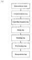
- FIG 1 is a flowchart showing the steps of the process for producing a semiconductor device.
- a semiconductor device is produced by a circuit formation step that provides a semiconductor wafer, and forms a circuit on the semiconductor wafer, a cured film formation step that forms a cured film that protects circuit wiring, a dicing step that dices the semiconductor wafer into semiconductor chips, a mounting step that mounts the semiconductor chip on a substrate, a wire bonding step that electrically connects the semiconductor chip to the substrate, and a encapsulation step that covers the semiconductor chip with a encapsulation resin.
- the present invention is characterized in that the cured film formed by the cured film formation step is formed of a cured material of a photosensitive resin composition that includes an alkali-soluble resin having a polybenzoxazole structure or a polybenzoxazole precursor structure, a compound that generates an acid upon exposure to light, and a solvent, the photosensitive resin composition substantially not containing N-methyl-2-pyrrolidone.
- a T-top phenomenon that may occur when using the chemically-amplified resist can be suppressed by the photosensitive resin composition that forms the cured film.
- the reason that the T-top phenomenon can be suppressed is considered to be as follows.
- a basic compound contained in the air is involved in the T-top phenomenon that may occur when using the chemically-amplified resist Specifically, an acid generated on the surface of the resist film upon exposure reacts with a basic compound contained in the air so that the acid is inactivated. Therefore, the amount of acid that is inactivated increases as the standing time before subjecting the resist film to post-exposure bake (PEB) increases, so that the solubility of the surface of the resist film decreases.
- PEB post-exposure bake
- N-methyl-2-pyrrolidone that is used as a solvent for the alkali-soluble resin having a polybenzoxazole structure or a polybenzoxazole precursor structure that forms the cured film is considered to cause the T-top phenomenon. Therefore, if the photosensitive resin composition substantially does not contain N-methyl-2-pyrrolidone, the amount of basic compound that causes the T-top phenomenon can be reduced.
- the chemically-amplified resist is applied to the semiconductor wafer.
- the chemically-amplified resist is then patterned, etched, and removed. This process is repeated to form a circuit
- Examples of the chemically-amplified resist include a composition prepared by mixing a base polymer (e.g., polyhydroxystyrene) in which a hydroxyl group is protected with a butoxycarbonyl (BOC) group or the like, a photoacid generator, and additives.
- the composition is alkali-insoluble, but becomes alkali-soluble when the photoacid generator is decomposed by exposure to ultraviolet rays to generate an acid so that the BOC group breaks.
- the photosensitive resin composition is applied to the uppermost layer of the semiconductor wafer on which the circuit is formed by the circuit formation step.
- the photosensitive resin composition is patterned and heated to form a cured film. A semiconductor chip having a protection function can thus be produced.
- the cured film formed by the cured film formation step is formed of a cured material of a photosensitive resin composition that includes an alkali-soluble resin having a polybenzoxazole structure or a polybenzoxazole precursor structure, a compound that generates an acid upon exposure to light, and a solvent, the photosensitive resin composition substantially not containing N-methyl-2-pyrrolidone (hereinafter may be referred to as "NMP").
- NMP N-methyl-2-pyrrolidone
- substantially not containing NMP refers to a case where the content of NMP in the photosensitive resin composition is 1 wt% or less, preferably 0.1 wt% or less, and particularly preferably 0 wt%, for example.
- the photosensitive resin composition does not contain NMP when the content of NMP is 0 wt%. If the content of NMP is within the above range, an increase in viscosity of the photosensitive resin composition can be suppressed in addition to effectively suppressing a T-top phenomenon.
- a photosensitive diazoquinone compound used as a positive-type photosensitizer causes discoloration of the resin composition in the presence of a basic compound. This is considered to be because the quinonediazide compound is gradually decomposed. It is considered that the viscosity of the photosensitive resin composition increases due to decomposition of the quinonediazide compound.
- the alkali-soluble resin has a polybenzoxazole structure or a polybenzoxazole precursor structure.
- the alkali-soluble resin may have other structures such as a polyimide structure, a polyimide precursor structure, or a polyamidate structure.
- Examples of the compound that generates an acid upon exposure to light include quinonediazide compounds, onium salts, halogenated organic compounds, ⁇ , ⁇ -bis(sulfonyl)diazomethane compounds, ⁇ -carbonyl-a-sulfonyl-diazomethane compounds, sulfone compounds, organic ester compounds, organic acid amide compounds, organic acid imide compounds, and the like.
- the content of the compound that generates an acid upon exposure to light is not particularly limited, but is preferably 1 to 50 parts by weight, and particularly preferably 5 to 30 parts by weight, based on 100 parts by weight of the alkali-soluble resin. If the content of the compound that generates an acid upon exposure to light is within the above range, the photosensitive resin composition has excellent photosensitivity, and the cured film has excellent properties.
- Examples of the solvent include ⁇ -butyrolactone, dimethyl sulfoxide, diethylene glycol dimethyl ether, diethylene glycol diethyl ether, diethylene glycol dibutyl ether, propylene glycol monomethyl ether, dipropylene glycol monomethyl ether, propylene glycol monomethyl ether acetate, methyl lactate, ethyl lactate, butyl lactate, methyl-1,3-butylene glycol acetate, 1,3-butylene glycol 3-monomethyl ether, methyl pyruvate, ethyl pyruvate, methyl-3-methoxypropionate, and the like. These solvents may be used either individually or in combination.
- a photosensitive resin composition which substantially does not contain NMP may be produced by avoiding use of NMP as the solvent of the resin composition, or using a raw material that substantially does not contain NMP, for example.
- NMP is generally used as a reaction solvent when synthesizing an alkali-soluble resin. After completion of the reaction, the product is re-precipitated in a poor solvent to obtain a resin, followed by purification and drying. In this case, NMP generally remains in the resin. In order to reduce the content of NMP, it is effective to dissolve the resin in a solvent other than NMP, followed by re-precipitation, purification, and drying. It is also effective to synthesize the alkali-soluble resin using a solvent other than NMP. This ensures that the resulting resin composition substantially does not contain NMP.
- the photosensitive resin composition preferably contains a phenol compound. This makes it possible to implement patterning with high sensitivity without causing the resin (scum) to remain after development.
- phenol compound examples include compounds shown by the following formulas. Note that the phenol compound is not limited to the following compounds.
- phenol compounds may be used either individually or in combination.
- the phenol compound is preferably used in an amount of 0.5 to 30 parts by weight, and particularly preferably 1 to 20 parts by weight, based on 100 parts by weight of the alkali-soluble resin. If the content of the phenol compound is within the above range, the cured film formed of the photosensitive resin composition has excellent properties.
- the photosensitive resin composition according to the present invention may further include additives such a leveling agent and a silane coupling agent, as required.
- the photosensitive resin composition having the above composition is applied to the surface of the semiconductor wafer by a normal wafer process, patterned, and heated at 250°C or higher to form a cured film.
- the semiconductor wafer on which the cured film is formed is diced to obtain semiconductor chips.
- a dicing sheet is bonded to the side of the semiconductor wafer opposite to the side on which the cured film is formed, and a ring is disposed around the semiconductor wafer to secure the semiconductor wafer.
- the semiconductor wafer is then cut (diced) using a blade.
- the dicing sheet is expanded using an expansion apparatus so that the diced semiconductor chips are separated at a given interval, and each semiconductor chip is picked up and placed on a substrate.
- the dicing sheet is cured by applying ultraviolet rays using an ultraviolet exposure apparatus in a state in which the semiconductor chips (semiconductor wafer) are positioned on the dicing sheet This reduces the adhesion of the dicing sheet.
- the semiconductor chip semiconductor wafer
- the semiconductor wafer is then placed in the expansion apparatus in a state in which the dicing sheet is bonded to the semiconductor wafer.
- the dicing sheet is expanded using the expansion apparatus so that the diced semiconductor chips are separated at a given interval.
- the semiconductor chip is then pushed up using a needle of an ejector head.
- the semiconductor chip pushed up using the needle is picked up using a vacuum collet, air tweezers, or the like, and mounted on a given substrate or the like.
- a gold wire having a diameter of 25 ⁇ m is bonded to bonding pads of the semiconductor chip and the substrate or the like using an automatic wire bonder while applying heat and ultrasonic vibrations, for example.
- a encapsulation resin composition in the form of tablets is injected into a mold at 180°C using a low-pressure transfer molding machine, and molded to encapsulat the substrate or the like on which the semiconductor chip is mounted, for example.
- the molded product is post-cured at 175°C for four hours.
- a semiconductor device shown in FIG 2 is obtained by the above method.
- FIG 2 is an enlarged cross-sectional view showing a pad area of a semiconductor device according to the present invention that has a bump.
- a semiconductor device 100 shown in FIG 2 an input/output Al pad 2 is provided on a silicon substrate 1 on which a semiconductor chip and wiring are formed.
- a passivation film 3 is formed on the silicon substrate 1, and a via hole is formed in the passivation film 3.
- the photosensitive resin composition is applied to the passivation film 3, patterned and heated to form a buffer coat film 4 (cured film).
- a metal film 5 is formed to be connected to the Al pad 2.
- a wiring section 6 is provided on the side of the metal film 5 opposite to the side that faces the Al pad 2.
- An insulating film 7 is formed to cover the wiring section 6 and the exposed area of the metal film 5.
- a through-hole is formed in the insulating film 7, a barrier metal 8 that electrically connects the wiring section 6 and a solder bump 9 being provided in the through-hole.
- a quinonediazide compound (B-1) shown by the following formula (manufactured by Toyo Gosei Co., Ltd.) was used as the compound that generates an acid upon exposure to light.
- Q 1 , Q 2 , and Q 3 are groups shown by the formula (1), and 25% of Q 1 , Q 2 , and Q 3 are hydrogen atoms.
- an input/output Al pad 2 was provided on a silicon substrate 1 on which a semiconductor chip and wiring were formed.
- a passivation film 3 was formed on the silicon substrate 1, and a via hole was formed in the passivation film 3.
- the photosensitive resin composition was applied to the passivation film 3, patterned and heated to form a buffer coat film 4 (cured film).
- a metal film 5 was formed to be connected to the Al pad 2.
- a wiring section 6 was provided on the side of the metal film 5 opposite to the side facing the Al pad 2.
- An insulating film 7 was formed to cover the wiring section 6 and the exposed area of the metal film 5.
- a through-hole was formed in the insulating film 7, and a barrier metal 8 that electrically connects the wiring section 6 and a solder bump 9 was provided in the through-hole.
- a semiconductor device 100 was thus produced in high yield, and showed high reliability.
- a dicarboxylic acid derivative was produced in the same manner as in Example 1.
- a polybenzoxazole precursor was produced in the same manner as in Example 1. except for using NMP instead of 1000g of ⁇ -butyrolactone.
- NMP 1000g of ⁇ -butyrolactone.
- 3 50 g of the resulting resin was dissolved in 1400 g of ⁇ -butyrolactone.
- the polybenzoxazole precursor resin and the quinonediazide compound used in Example 1 were dissolved in ⁇ -butyrolactone. The solution was filtered through a fluororesin filter having a pore size of 0.2 ⁇ m to obtain a positive-type photosensitive resin composition.
- the NMP content in the photosensitive resin composition measured in the same manner as in Example 1 was 0.8 wt%.
- Dicyclohexylcarbodiurea that precipitated was removed by filtration. Then, 6000 g of purified water was added dropwise to the filtrate. The precipitate was collected by filtration, sufficiently washed with isopropyl alcohol, and dried under vacuum to obtain the target dicarboxylic acid derivative.
- the polybenzoxazole precursor resin and the quinonediazide compound used in Example 1 were dissolved in ⁇ -butyrolactone. The solution was filtered through a fluororesin filter having a pore size of 0.2 ⁇ m to obtain a positive-type photosensitive resin composition.
- the NMP content in the photosensitive resin composition measured in the same manner as in Example 1 was 0.01 wt% or less (equal to or less than the detection limit).
- a photosensitive resin composition was prepared in the same manner as in Example 2 using the polybenzoxazole precursor resin (A-4) that was not re-purified.
- the NMP content in the photosensitive resin composition was 2.6 wt%.
- the NMP concentration when spin-coating the photosensitive resin composition was analyzed by thermal desorption-gas chromatograph mass spectrometry. Specifically, the photosensitive resin composition was applied to a silicon wafer. The silicon wafer was rotated at 800 rpm for five seconds and at 1500 rpm for 30 seconds. NMP was sampled by adsorption at a position about 10 cm above the rotating wafer. Analysis was conducted using the following apparatus to determine the NMP concentration.
- the photosensitive resin composition was stored in a yellow room at room temperature.
- the viscosity of the photosensitive resin composition was measured on the first day and the fourteenth day using a viscometer ("VISCOMETER-TV-22" manufactured by Toki Sangyo Co., Ltd.).
- the increase rate of the viscosity measured on the fourteenth day with respect to the viscosity measured on the first day was calculated.
- the photosensitive resin composition was applied to a semiconductor wafer using a spin coater, and prebaked on a hot plate at 120°C for four minutes to obtain a film having a thickness of about 7.5 ⁇ m.
- the film was exposed at a dose of 500 mJ/cm 2 using an i-line stepper ("4425i" manufactured by Nikon Corporation) through a mask manufactured by Toppan Printing Co., Ltd. (test chart No. 1 in which a line pattern and a space pattern having a width of 0.88 to 50 ⁇ m were drawn).
- the film was rinsed with purified water for 10 seconds.
- the semiconductor wafer was then observed using a microscope to determine the resolution.
- the photosensitive resin composition was applied to a semiconductor wafer so that the thickness after curing was about 10 ⁇ m.
- the photosensitive resin composition was cured in a clean oven at 150°C for 30 minutes and at 320°C for 30 minutes in an atmosphere having an oxygen concentration of 10 ppm or less.
- the cured film was immersed in a 2% hydrogen fluoride aqueous solution to remove the cured film from the silicon wafer.
- the cured film was sufficiently washed with purified water, and dried in an oven at 60°C for five hours.
- the cured film was cut in the shape of a strip having a width of 10 mm to obtain a tensile test specimen. The tensile elongation of the specimen was measured using a tensile tester.
- the volatile NMP amount was small in Examples 1 to 3 since the NMP content was low. This suggests that a T-top phenomenon can be suppressed.
- Example 1 excellent resolution and tensile elongation were also achieved.
- the present invention provides a process for producing a semiconductor device that ensures high productivity.
- the present invention may also be applied when using a protective film in the production of liquid crystal displays and the like.
Landscapes
- Chemical & Material Sciences (AREA)
- Physics & Mathematics (AREA)
- Organic Chemistry (AREA)
- Chemical Kinetics & Catalysis (AREA)
- General Physics & Mathematics (AREA)
- Spectroscopy & Molecular Physics (AREA)
- Polymers & Plastics (AREA)
- Medicinal Chemistry (AREA)
- Health & Medical Sciences (AREA)
- Life Sciences & Earth Sciences (AREA)
- Engineering & Computer Science (AREA)
- Materials Engineering (AREA)
- Wood Science & Technology (AREA)
- Materials For Photolithography (AREA)
- Formation Of Insulating Films (AREA)
- Internal Circuitry In Semiconductor Integrated Circuit Devices (AREA)
- Macromolecular Compounds Obtained By Forming Nitrogen-Containing Linkages In General (AREA)
- Exposure And Positioning Against Photoresist Photosensitive Materials (AREA)
Abstract
Description
- The present invention relates to a process for producing a semiconductor device.
- A polybenzoxazole resin or a polyimide resin that has excellent heat resistance, superior electrical and mechanical properties, and the like has been used to produce a surface protective film or an interlayer dielectric of semiconductor devices. A positive-type photosensitive resin composition that contains a polybenzoxazole resin or a polyimide resin and a quinonediazide compound (photosensitizer) has been used to simplify the production process (Patent Document 1).
- When producing a semiconductor device, a deposition step that forms an oxide film or the like, a lithography step that forms a circuit, and an impurity addition (implantation) step are repeated. The lithography step utilizes a chemically-amplified resist. After completion of the lithography step, a semiconductor wafer protective film is formed using a polybenzoxazole resin or a polyimide resin. Therefore, the chemically-amplified photoresist and the polybenzoxazole resin or the polyimide resin may be used in semiconductor production lines that are close together.
- When using the chemically-amplified resist, a T-top phenomenon (i.e., the upper area of the pattern has a width larger than that of the lower area) or the like may occur. (Patent Document 1)
JP-A-1-46862 - An object of the present invention is to provide a process for producing a semiconductor device that can suppress a T-top phenomenon or the like that may occur when forming a circuit on a semiconductor wafer using a chemically-amplified resist in the production of semiconductor devices.
- According to the present invention, the above object can be achieved by the following process for producing a semiconductor device.
- (1) A process for producing a semiconductor device comprising a circuit formation step of forming circuit wiring on a semiconductor wafer using a chemically-amplified resist, and a cured film formation step of forming a cured film that protects the circuit wiring after forming the circuit wiring, the cured film being formed of a cured material of a photosensitive resin composition that comprises an alkali-soluble resin having a polybenzoxazole structure or a polybenzoxazole precursor structure, a compound that generates an acid upon exposure to light, and a solvent, the photosensitive resin composition substantially not containing N-methyl-2-pyrrolidone.
- (2) The process according to (1), wherein the content of N-methyl-2-pyrrolidone in the photosensitive resin composition is 1 wt% or less.
- (3) The process according to (1), wherein the content of N-methyl-2-pyrrolidone in the photosensitive resin composition is 0.1 wt% or less.
- (4) The process according to (1), wherein the content of N-methyl-2-pyrrolidone in the photosensitive resin composition is 0 wt% or less.
- According to the present invention, a process for producing a semiconductor device that can suppress a T-top phenomenon that may occur when forming a circuit on a semiconductor wafer using a chemically-amplified resist, can be provided.
-
-
FIG 1 is a flowchart showing semiconductor device production steps, andFIG 2 is a cross-sectional view showing an example of a semiconductor device. - The process for producing a semiconductor device according to the present invention is described below.
-
FIG 1 is a flowchart showing the steps of the process for producing a semiconductor device. - As shown in
FIG 1 , a semiconductor device is produced by a circuit formation step that provides a semiconductor wafer, and forms a circuit on the semiconductor wafer, a cured film formation step that forms a cured film that protects circuit wiring, a dicing step that dices the semiconductor wafer into semiconductor chips, a mounting step that mounts the semiconductor chip on a substrate, a wire bonding step that electrically connects the semiconductor chip to the substrate, and a encapsulation step that covers the semiconductor chip with a encapsulation resin. - The present invention is characterized in that the cured film formed by the cured film formation step is formed of a cured material of a photosensitive resin composition that includes an alkali-soluble resin having a polybenzoxazole structure or a polybenzoxazole precursor structure, a compound that generates an acid upon exposure to light, and a solvent, the photosensitive resin composition substantially not containing N-methyl-2-pyrrolidone.
- A T-top phenomenon that may occur when using the chemically-amplified resist can be suppressed by the photosensitive resin composition that forms the cured film. The reason that the T-top phenomenon can be suppressed is considered to be as follows.
- A basic compound contained in the air is involved in the T-top phenomenon that may occur when using the chemically-amplified resist Specifically, an acid generated on the surface of the resist film upon exposure reacts with a basic compound contained in the air so that the acid is inactivated. Therefore, the amount of acid that is inactivated increases as the standing time before subjecting the resist film to post-exposure bake (PEB) increases, so that the solubility of the surface of the resist film decreases. N-methyl-2-pyrrolidone that is used as a solvent for the alkali-soluble resin having a polybenzoxazole structure or a polybenzoxazole precursor structure that forms the cured film is considered to cause the T-top phenomenon. Therefore, if the photosensitive resin composition substantially does not contain N-methyl-2-pyrrolidone, the amount of basic compound that causes the T-top phenomenon can be reduced.
- Each step is described below.
- In the circuit formation step, the chemically-amplified resist is applied to the semiconductor wafer. The chemically-amplified resist is then patterned, etched, and removed. This process is repeated to form a circuit
- Examples of the chemically-amplified resist include a composition prepared by mixing a base polymer (e.g., polyhydroxystyrene) in which a hydroxyl group is protected with a butoxycarbonyl (BOC) group or the like, a photoacid generator, and additives. The composition is alkali-insoluble, but becomes alkali-soluble when the photoacid generator is decomposed by exposure to ultraviolet rays to generate an acid so that the BOC group breaks.
- In the cured film formation step, the photosensitive resin composition is applied to the uppermost layer of the semiconductor wafer on which the circuit is formed by the circuit formation step. The photosensitive resin composition is patterned and heated to form a cured film. A semiconductor chip having a protection function can thus be produced.
- The cured film formed by the cured film formation step is formed of a cured material of a photosensitive resin composition that includes an alkali-soluble resin having a polybenzoxazole structure or a polybenzoxazole precursor structure, a compound that generates an acid upon exposure to light, and a solvent, the photosensitive resin composition substantially not containing N-methyl-2-pyrrolidone (hereinafter may be referred to as "NMP"). This suppresses a T-top phenomenon that may occur when using the chemically-amplified resist.
- The expression "substantially not containing NMP" refers to a case where the content of NMP in the photosensitive resin composition is 1 wt% or less, preferably 0.1 wt% or less, and particularly preferably 0 wt%, for example. The photosensitive resin composition does not contain NMP when the content of NMP is 0 wt%. If the content of NMP is within the above range, an increase in viscosity of the photosensitive resin composition can be suppressed in addition to effectively suppressing a T-top phenomenon.
- Suppression of an increase in viscosity of the photosensitive resin composition when the photosensitive resin composition substantially does not contain NMP is considered to be caused by the following reason. A photosensitive diazoquinone compound used as a positive-type photosensitizer causes discoloration of the resin composition in the presence of a basic compound. This is considered to be because the quinonediazide compound is gradually decomposed. It is considered that the viscosity of the photosensitive resin composition increases due to decomposition of the quinonediazide compound.
- The alkali-soluble resin has a polybenzoxazole structure or a polybenzoxazole precursor structure. The alkali-soluble resin may have other structures such as a polyimide structure, a polyimide precursor structure, or a polyamidate structure.
- Examples of the compound that generates an acid upon exposure to light include quinonediazide compounds, onium salts, halogenated organic compounds, α,α-bis(sulfonyl)diazomethane compounds, α-carbonyl-a-sulfonyl-diazomethane compounds, sulfone compounds, organic ester compounds, organic acid amide compounds, organic acid imide compounds, and the like.
- The content of the compound that generates an acid upon exposure to light is not particularly limited, but is preferably 1 to 50 parts by weight, and particularly preferably 5 to 30 parts by weight, based on 100 parts by weight of the alkali-soluble resin. If the content of the compound that generates an acid upon exposure to light is within the above range, the photosensitive resin composition has excellent photosensitivity, and the cured film has excellent properties.
- Examples of the solvent include γ-butyrolactone, dimethyl sulfoxide, diethylene glycol dimethyl ether, diethylene glycol diethyl ether, diethylene glycol dibutyl ether, propylene glycol monomethyl ether, dipropylene glycol monomethyl ether, propylene glycol monomethyl ether acetate, methyl lactate, ethyl lactate, butyl lactate, methyl-1,3-butylene glycol acetate, 1,3-butylene glycol 3-monomethyl ether, methyl pyruvate, ethyl pyruvate, methyl-3-methoxypropionate, and the like. These solvents may be used either individually or in combination.
- A photosensitive resin composition which substantially does not contain NMP may be produced by avoiding use of NMP as the solvent of the resin composition, or using a raw material that substantially does not contain NMP, for example.
- NMP is generally used as a reaction solvent when synthesizing an alkali-soluble resin. After completion of the reaction, the product is re-precipitated in a poor solvent to obtain a resin, followed by purification and drying. In this case, NMP generally remains in the resin. In order to reduce the content of NMP, it is effective to dissolve the resin in a solvent other than NMP, followed by re-precipitation, purification, and drying. It is also effective to synthesize the alkali-soluble resin using a solvent other than NMP. This ensures that the resulting resin composition substantially does not contain NMP.
- The photosensitive resin composition preferably contains a phenol compound. This makes it possible to implement patterning with high sensitivity without causing the resin (scum) to remain after development.
- Examples of the phenol compound include compounds shown by the following formulas. Note that the phenol compound is not limited to the following compounds.
- These phenol compounds may be used either individually or in combination.


- The phenol compound is preferably used in an amount of 0.5 to 30 parts by weight, and particularly preferably 1 to 20 parts by weight, based on 100 parts by weight of the alkali-soluble resin. If the content of the phenol compound is within the above range, the cured film formed of the photosensitive resin composition has excellent properties.
- The photosensitive resin composition according to the present invention may further include additives such a leveling agent and a silane coupling agent, as required.
- The photosensitive resin composition having the above composition is applied to the surface of the semiconductor wafer by a normal wafer process, patterned, and heated at 250°C or higher to form a cured film.
- In the dicing step, the semiconductor wafer on which the cured film is formed is diced to obtain semiconductor chips.
- For example, a dicing sheet is bonded to the side of the semiconductor wafer opposite to the side on which the cured film is formed, and a ring is disposed around the semiconductor wafer to secure the semiconductor wafer. The semiconductor wafer is then cut (diced) using a blade.
- In the mounting step, the dicing sheet is expanded using an expansion apparatus so that the diced semiconductor chips are separated at a given interval, and each semiconductor chip is picked up and placed on a substrate.
- Specifically, the dicing sheet is cured by applying ultraviolet rays using an ultraviolet exposure apparatus in a state in which the semiconductor chips (semiconductor wafer) are positioned on the dicing sheet This reduces the adhesion of the dicing sheet. The semiconductor chip (semiconductor wafer) can be easily picked up by thus reducing the adhesion of the dicing sheet to the semiconductor wafer. The semiconductor wafer is then placed in the expansion apparatus in a state in which the dicing sheet is bonded to the semiconductor wafer. The dicing sheet is expanded using the expansion apparatus so that the diced semiconductor chips are separated at a given interval. The semiconductor chip is then pushed up using a needle of an ejector head.
- The semiconductor chip pushed up using the needle is picked up using a vacuum collet, air tweezers, or the like, and mounted on a given substrate or the like.
- In the wire bonding step, a gold wire having a diameter of 25 µm is bonded to bonding pads of the semiconductor chip and the substrate or the like using an automatic wire bonder while applying heat and ultrasonic vibrations, for example.
- In the encapsulation step, a encapsulation resin composition in the form of tablets is injected into a mold at 180°C using a low-pressure transfer molding machine, and molded to encapsulat the substrate or the like on which the semiconductor chip is mounted, for example. The molded product is post-cured at 175°C for four hours.
- A semiconductor device shown in
FIG 2 is obtained by the above method. -
FIG 2 is an enlarged cross-sectional view showing a pad area of a semiconductor device according to the present invention that has a bump. In asemiconductor device 100 shown inFIG 2 , an input/output Al pad 2 is provided on a silicon substrate 1 on which a semiconductor chip and wiring are formed. A passivation film 3 is formed on the silicon substrate 1, and a via hole is formed in the passivation film 3. The photosensitive resin composition is applied to the passivation film 3, patterned and heated to form a buffer coat film 4 (cured film). Ametal film 5 is formed to be connected to theAl pad 2. A wiring section 6 is provided on the side of themetal film 5 opposite to the side that faces theAl pad 2. An insulatingfilm 7 is formed to cover the wiring section 6 and the exposed area of themetal film 5. A through-hole is formed in the insulatingfilm 7, abarrier metal 8 that electrically connects the wiring section 6 and a solder bump 9 being provided in the through-hole. - The present invention is further described below by way of examples and a comparative example. Note that the present invention is not limited to the following examples.
- 258.2 g (1 mol) of diphenyl ether-4,4'-dicarboxylic acid and 270.3 g (2 mol) of 1-hydroxybenzotriazole were dissolved in 1500 g of NMP. 412.7 g (2 mol) of dicyclohexylcarbodiimide dissolved in 500 g of NMP was added dropwise to the solution while cooling the reaction system at 0 to 5°C. After the addition, the reaction system was allowed to return to room temperature, and stirred for 12 hours. After completion of the reaction, dicyclohexylcarbodiurea that precipitated was removed by filtration. Then, 2000 g of purified water was added dropwise to the filtrate. The precipitate was collected by filtration, sufficiently washed with isopropyl alcohol, and dried under vacuum to obtain the target dicarboxylic acid derivative.
- 217.2 g (0.593 mol) of hexafluoro-2,2-bis(3-amino-4-hydroxyphenyl)propane and 236.6 g (0.480 mol) of the dicarboxylic acid derivative were dissolved in 1000 g of γ-butyrolactone. The reaction system was heated to 80°C and allowed to react for 12 hours. After the addition of 46.2 g (0.281 mol) of 5-norbornene-2,3-dicarboxylic anhydride dissolved in 230 g of γ-butyrolactone, the mixture was allowed to react for three hours. The reaction mixture was added to a water/TPA (=3/1) solution, and the precipitate was collected, sufficiently washed with purified water, and dried under vacuum to obtain the target polybenzoxazole precursor resin (A-1).
- A quinonediazide compound (B-1) shown by the following formula (manufactured by Toyo Gosei Co., Ltd.) was used as the compound that generates an acid upon exposure to light.

- 24 g of the polybenzoxazole precursor resin (A-1) and 4.8 g of the compound (B-1) that generates an acid upon exposure to light were dissolved in 65 g of γ-butyrolactone. The solution was filtered through a fluororesin filter having a pore size of 0.2 µm to obtain a positive-type photosensitive resin composition. The NMP content in the positive-type photosensitive resin composition was 0.01 wt% or less (equal to or less than the detection limit). The NMP content was measured using a gas chromatography system manufactured by Shimadzu Corporation. The measurement conditions are given below.
- Apparatus: GC-1700 manufactured by Shimadzu Corporation
- Column: DB-5 manufactured by J & D (30 m×0.25 µm)
- As shown in
FIG. 2 , an input/output Al pad 2 was provided on a silicon substrate 1 on which a semiconductor chip and wiring were formed. A passivation film 3 was formed on the silicon substrate 1, and a via hole was formed in the passivation film 3. The photosensitive resin composition was applied to the passivation film 3, patterned and heated to form a buffer coat film 4 (cured film). Ametal film 5 was formed to be connected to theAl pad 2. A wiring section 6 was provided on the side of themetal film 5 opposite to the side facing theAl pad 2. An insulatingfilm 7 was formed to cover the wiring section 6 and the exposed area of themetal film 5. A through-hole was formed in the insulatingfilm 7, and abarrier metal 8 that electrically connects the wiring section 6 and a solder bump 9 was provided in the through-hole. - A
semiconductor device 100 was thus produced in high yield, and showed high reliability. - A dicarboxylic acid derivative was produced in the same manner as in Example 1. A polybenzoxazole precursor was produced in the same manner as in Example 1. except for using NMP instead of 1000g of γ-butyrolactone. After the addition of 5-norbornene-2,3-dicarboxylic anhydride dissolved in 230 g of NMP, the mixture was allowed to react for three hours. The reaction mixture was added to a water/IPA (=3/1) solution, and the precipitate was collected, sufficiently washed with purified water, and dried under vacuum to obtain a polybenzoxazole precursor resin (A-4). 3 50 g of the resulting resin was dissolved in 1400 g of γ-butyrolactone. The solution was added to a water/IPA (=3/1) solution, and the precipitate was collected, sufficiently washed with purified water, and dried under vacuum to obtain the target polybenzoxazole precursor resin (A-2) that had been re-purified.
- The polybenzoxazole precursor resin and the quinonediazide compound used in Example 1 were dissolved in γ-butyrolactone. The solution was filtered through a fluororesin filter having a pore size of 0.2 µm to obtain a positive-type photosensitive resin composition.
- The NMP content in the photosensitive resin composition measured in the same manner as in Example 1 was 0.8 wt%.
- 244.0 g (0.945 mol) of diphenyl ether-4,4'-dicarboxylic acid and 255.4 g (1.890 mol) of 1-hydroxybenzotriazole were dissolved in 8000 g of γ-butyrolactone. 390.0 g (1.890 mol) of dicyclohexylcarbodiimide dissolved in 500 g of γ-butyrolactone was added dropwise to the solution while cooling the reaction system at 0 to 5°C. After the addition, the temperature of the reaction system was adjusted to 35°C, and the mixture was stirred for 12 hours. Then, the mixture was heated to 55°C using an oil bath, and stirred for 20 minutes, followed by hot filtration. Dicyclohexylcarbodiurea that precipitated was removed by filtration. Then, 6000 g of purified water was added dropwise to the filtrate. The precipitate was collected by filtration, sufficiently washed with isopropyl alcohol, and dried under vacuum to obtain the target dicarboxylic acid derivative.
- 217.2 g (0.593 mol) of hexafluoro-2,2-bis(3-amino-4-hydroxyphenyl)propane and 236.6 g (0.480 mol) of the dicarboxylic acid derivative were dissolved in 1000 g of γ-butyrolactone. The reaction system was heated to 80°C and allowed to react for 12 hours. After the addition of 46.2 g (0.281 mol) of 5-norbornene-2,3-dicarboxylic anhydride dissolved in 230 g of γ-butyrolactone, the mixture was allowed to react for three hours. The reaction mixture was added to a water/IPA (=3/1) solution, and the precipitate was collected, sufficiently washed with purified water, and dried under vacuum to obtain the target polybenzoxazole precursor resin (A-3).
- The polybenzoxazole precursor resin and the quinonediazide compound used in Example 1 were dissolved in γ-butyrolactone. The solution was filtered through a fluororesin filter having a pore size of 0.2 µm to obtain a positive-type photosensitive resin composition.
- The NMP content in the photosensitive resin composition measured in the same manner as in Example 1 was 0.01 wt% or less (equal to or less than the detection limit).
- A photosensitive resin composition was prepared in the same manner as in Example 2 using the polybenzoxazole precursor resin (A-4) that was not re-purified. The NMP content in the photosensitive resin composition was 2.6 wt%.
- The semiconductor devices obtained in the examples and the comparative example were evaluated as follows. The evaluation items and methods are given below. The results are shown in Table 1.
- The NMP concentration when spin-coating the photosensitive resin composition was analyzed by thermal desorption-gas chromatograph mass spectrometry. Specifically, the photosensitive resin composition was applied to a silicon wafer. The silicon wafer was rotated at 800 rpm for five seconds and at 1500 rpm for 30 seconds. NMP was sampled by adsorption at a position about 10 cm above the rotating wafer. Analysis was conducted using the following apparatus to determine the NMP concentration.
-
- Thermal desorption cooling trap manufactured by CHROMPACK (CP 4020)
- Gas chromatograph-mass spectrometer manufactured by Agilent (5973N)
- The photosensitive resin composition was stored in a yellow room at room temperature. The viscosity of the photosensitive resin composition was measured on the first day and the fourteenth day using a viscometer ("VISCOMETER-TV-22" manufactured by Toki Sangyo Co., Ltd.). The increase rate of the viscosity measured on the fourteenth day with respect to the viscosity measured on the first day was calculated.
- The photosensitive resin composition was applied to a semiconductor wafer using a spin coater, and prebaked on a hot plate at 120°C for four minutes to obtain a film having a thickness of about 7.5 µm. The film was exposed at a dose of 500 mJ/cm2 using an i-line stepper ("4425i" manufactured by Nikon Corporation) through a mask manufactured by Toppan Printing Co., Ltd. (test chart No. 1 in which a line pattern and a space pattern having a width of 0.88 to 50 µm were drawn). After removing the exposed area by immersing the film in a 2.38% tetramethylammonium hydroxide aqueous solution for 30 seconds, the film was rinsed with purified water for 10 seconds. The semiconductor wafer was then observed using a microscope to determine the resolution.
- The photosensitive resin composition was applied to a semiconductor wafer so that the thickness after curing was about 10 µm. The photosensitive resin composition was cured in a clean oven at 150°C for 30 minutes and at 320°C for 30 minutes in an atmosphere having an oxygen concentration of 10 ppm or less.
- The cured film was immersed in a 2% hydrogen fluoride aqueous solution to remove the cured film from the silicon wafer. The cured film was sufficiently washed with purified water, and dried in an oven at 60°C for five hours. The cured film was cut in the shape of a strip having a width of 10 mm to obtain a tensile test specimen. The tensile elongation of the specimen was measured using a tensile tester.
TABLE 1 Example 1 Example 2 Example 3 Comparative Example 1 Alkali-soluble resin PBO*1 precursor PBO*1 precursor PBO*1 precursor PBO*1 precursor A-1 A-2 A-3 A-4 Compound that generates acid Quinonediazide compound Quinonediazide compound Quinonediazide compound Quinonediazide compound B-1 B-1 B-1 B-1 Solvent GBL*2 GBL*2 GBL*2 GBL*2 NMP content <0.01 wt% 0.8 wt% <0.01 wt% 2.6 wt% Viscosity increase rate 4% 7% 3% 12% Volatile NMP amount <10 ppb 27 ppb <10 ppb 190 ppb (T-top phenomenon suppression effect) Resolution 5 µm 5 µm 5 µm 5 µm Cured film properties (tensile elongation) 51% 48% 55% 25% *1 Polybenzoxazole
*2 γ-Butyrolactone - As shown in Table 1, the volatile NMP amount was small in Examples 1 to 3 since the NMP content was low. This suggests that a T-top phenomenon can be suppressed.
- In Examples 1 to 3, the viscosity increase rate was also small. This indicates excellent storage stability.
- In Example 1 and 2, excellent resolution and tensile elongation were also achieved.
- 1: Semiconductor wafer
- 2: A1 pad
- 3: Passivation film
- 4: Buffer coat film
- 5: Metal film
- 6: Wiring section
- 7: Insulating film
- 8: Barrier metal
- 9: Solder bump
- 100: Semiconductor device
- The present invention provides a process for producing a semiconductor device that ensures high productivity.
- The present invention may also be applied when using a protective film in the production of liquid crystal displays and the like.
Claims (4)
- A process for producing a semiconductor device comprising a circuit formation step of forming circuit wiring on a semiconductor wafer using a chemically-amplified resist, and a cured film formation step of forming a cured film that protects the circuit wiring after forming the circuit wiring, the cured film being formed of a cured material of a photosensitive resin composition that comprises an alkali-soluble resin having a polybenzoxazole structure or a polybenzoxazole precursor structure, a compound that generates an acid upon exposure to light, and a solvent, the photosensitive resin composition substantially not containing N-methyl-2-pyrrolidone.
- The process according to claim 1, wherein the content of N-methyl-2-pyrrolidone in the photosensitive resin composition is 1 wt% or less.
- The process according to claim 1, wherein the content of N-methyl-2-pyrrolidone in the photosensitive resin composition is 0.1 wt% or less.
- The process according to claim 1, wherein the content of N-methyl-2-pyrrolidone in the photosensitive resin composition is 0 wt%.
Applications Claiming Priority (3)
| Application Number | Priority Date | Filing Date | Title |
|---|---|---|---|
| JP2007159671 | 2007-06-18 | ||
| JP2008152020A JP5332326B2 (en) | 2007-06-18 | 2008-06-10 | Manufacturing method of semiconductor device |
| PCT/JP2008/061385 WO2008156190A1 (en) | 2007-06-18 | 2008-06-17 | Process for producing semiconductor device |
Publications (3)
| Publication Number | Publication Date |
|---|---|
| EP2159830A1 true EP2159830A1 (en) | 2010-03-03 |
| EP2159830A4 EP2159830A4 (en) | 2010-11-10 |
| EP2159830B1 EP2159830B1 (en) | 2014-01-08 |
Family
ID=40156344
Family Applications (1)
| Application Number | Title | Priority Date | Filing Date |
|---|---|---|---|
| EP08777503.7A Not-in-force EP2159830B1 (en) | 2007-06-18 | 2008-06-17 | Process for producing semiconductor device |
Country Status (8)
| Country | Link |
|---|---|
| US (1) | US8198006B2 (en) |
| EP (1) | EP2159830B1 (en) |
| JP (1) | JP5332326B2 (en) |
| KR (1) | KR101415441B1 (en) |
| CN (1) | CN101681834B (en) |
| MY (1) | MY149401A (en) |
| TW (1) | TWI446445B (en) |
| WO (1) | WO2008156190A1 (en) |
Families Citing this family (2)
| Publication number | Priority date | Publication date | Assignee | Title |
|---|---|---|---|---|
| US8487068B2 (en) * | 2011-08-31 | 2013-07-16 | Toho Chemical Industry Co., Ltd. | Method of manufacturing polybenzoxazole precursor |
| JP2020164657A (en) * | 2019-03-29 | 2020-10-08 | 住友ベークライト株式会社 | Method for Producing Polybenzoxazole and Photosensitive Resin Composition |
Family Cites Families (11)
| Publication number | Priority date | Publication date | Assignee | Title |
|---|---|---|---|---|
| JPS6446862A (en) | 1987-08-18 | 1989-02-21 | Fujitsu Ltd | Bus controller |
| JPH08162460A (en) * | 1994-12-09 | 1996-06-21 | Mitsubishi Electric Corp | Semiconductor device and method of manufacturing semiconductor device |
| JP3422691B2 (en) * | 1997-07-30 | 2003-06-30 | 住友ベークライト株式会社 | Positive photosensitive resin composition |
| KR100422971B1 (en) * | 1999-12-29 | 2004-03-12 | 삼성전자주식회사 | Ion-type Photoacid Generator Having Naphtol Structure and the Photosensitive Polyimide Composition Prepared by Using the Same |
| JP2004157248A (en) * | 2002-11-05 | 2004-06-03 | Hitachi Chemical Dupont Microsystems Ltd | Positive photosensitive resin composition, pattern production method and electronic component |
| JP4207581B2 (en) * | 2002-11-06 | 2009-01-14 | 日立化成デュポンマイクロシステムズ株式会社 | Heat-resistant photosensitive resin composition, method for producing relief pattern, and electronic component |
| EP1609024B1 (en) * | 2003-03-11 | 2015-09-30 | Fujifilm Electronic Materials USA, Inc. | Photosensitive resin compositions |
| JP4150660B2 (en) * | 2003-12-16 | 2008-09-17 | 松下電器産業株式会社 | Pattern formation method |
| JP2005281388A (en) * | 2004-03-29 | 2005-10-13 | Sumitomo Bakelite Co Ltd | Manufacturing method of polybenzoxazole precursor |
| JP4742634B2 (en) * | 2005-03-22 | 2011-08-10 | 住友ベークライト株式会社 | Resin composition and semiconductor device and display element using the same |
| US7803510B2 (en) * | 2005-08-17 | 2010-09-28 | Fujifilm Electronic Materials U.S.A., Inc. | Positive photosensitive polybenzoxazole precursor compositions |
-
2008
- 2008-06-10 JP JP2008152020A patent/JP5332326B2/en active Active
- 2008-06-17 CN CN2008800187082A patent/CN101681834B/en active Active
- 2008-06-17 KR KR1020097025092A patent/KR101415441B1/en active Active
- 2008-06-17 TW TW097122506A patent/TWI446445B/en active
- 2008-06-17 WO PCT/JP2008/061385 patent/WO2008156190A1/en not_active Ceased
- 2008-06-17 MY MYPI20095419A patent/MY149401A/en unknown
- 2008-06-17 EP EP08777503.7A patent/EP2159830B1/en not_active Not-in-force
- 2008-06-17 US US12/602,156 patent/US8198006B2/en not_active Expired - Fee Related
Also Published As
| Publication number | Publication date |
|---|---|
| KR101415441B1 (en) | 2014-07-04 |
| US20100183985A1 (en) | 2010-07-22 |
| TW200910455A (en) | 2009-03-01 |
| JP5332326B2 (en) | 2013-11-06 |
| US8198006B2 (en) | 2012-06-12 |
| CN101681834A (en) | 2010-03-24 |
| EP2159830B1 (en) | 2014-01-08 |
| EP2159830A4 (en) | 2010-11-10 |
| KR20100021427A (en) | 2010-02-24 |
| CN101681834B (en) | 2013-10-30 |
| TWI446445B (en) | 2014-07-21 |
| WO2008156190A1 (en) | 2008-12-24 |
| MY149401A (en) | 2013-08-30 |
| JP2009027151A (en) | 2009-02-05 |
Similar Documents
| Publication | Publication Date | Title |
|---|---|---|
| EP1965256B1 (en) | Positive photosensitive resin composition, and use of the same for manufacturing a semiconductor device and a display | |
| EP2196850B1 (en) | Cured film obtained using a positive photosensitive resin composition | |
| US8758977B2 (en) | Negative-type photosensitive resin composition, pattern forming method and electronic parts | |
| US6436593B1 (en) | Positive photosensitive resin composition, process for producing pattern and electronic parts | |
| EP2083326B1 (en) | Photosensitive resin composition, insulating film, protective film, and electronic equipment | |
| EP3660077A1 (en) | Siloxane polymer containing isocyanuric acid and polyether skeletons, photosensitive resin composition, pattern forming process, and fabrication of opto-semiconductor device | |
| CN1341279A (en) | Semiconductor device | |
| KR100833706B1 (en) | Photosensitive polyimide composition, polyimide film and semiconductor device using the same | |
| KR100829291B1 (en) | Method of manufacturing semiconductor device | |
| EP2159830B1 (en) | Process for producing semiconductor device | |
| EP2306244B1 (en) | Positive photosensitive resin composition, cured film and use of the cured film | |
| KR102670213B1 (en) | Positive photosensitive resin composition, positive photosensitive dry film, method for producing positive photosensitive dry film, patterning process, method for forming cured film, interlayer insulation film, surface protective film, and electronic component | |
| JP5099979B2 (en) | Negative photosensitive resin composition, pattern manufacturing method, and electronic component | |
| JP2006178059A (en) | Negative photosensitive resin composition, method for producing pattern and electronic component | |
| EP3413132B1 (en) | Positive-type photosensitive resin composition | |
| TW202136373A (en) | Positive photosensitive resin composition | |
| CN115113484B (en) | Positive photosensitive resin composition, positive photosensitive dry film, method for producing positive photosensitive dry film, and method for forming pattern | |
| KR102642893B1 (en) | Photosensitive resin composition | |
| EP4664197A1 (en) | Photosensitive resin composition, photosensitive resin coating film, photosensitive dry film, and pattern formation method | |
| KR101025395B1 (en) | Negative photosensitive resin composition, manufacturing method of pattern and electronic part | |
| CN118108661B (en) | A diamine monomer having nitrogen heterocycle and benzocyclobutene structure and preparation method and application thereof | |
| KR20260034493A (en) | Photosensitive resin composition, photosensitive resin layer and semiconductor device using the same | |
| WO2024070845A1 (en) | Photosensitive resin composition, photosensitive resin sheet, cured product, cured product production method, semiconductor device, display device, and resin production method | |
| WO2025072607A1 (en) | Photosensitive composition containing pfas free polycycloolefinic terpolymers and semiconductor device made thereof | |
| KR101202010B1 (en) | Positive photoresist composition |
Legal Events
| Date | Code | Title | Description |
|---|---|---|---|
| PUAI | Public reference made under article 153(3) epc to a published international application that has entered the european phase |
Free format text: ORIGINAL CODE: 0009012 |
|
| 17P | Request for examination filed |
Effective date: 20091217 |
|
| AK | Designated contracting states |
Kind code of ref document: A1 Designated state(s): AT BE BG CH CY CZ DE DK EE ES FI FR GB GR HR HU IE IS IT LI LT LU LV MC MT NL NO PL PT RO SE SI SK TR |
|
| AX | Request for extension of the european patent |
Extension state: AL BA MK RS |
|
| DAX | Request for extension of the european patent (deleted) | ||
| A4 | Supplementary search report drawn up and despatched |
Effective date: 20101007 |
|
| RIC1 | Information provided on ipc code assigned before grant |
Ipc: H01L 23/522 20060101ALI20101001BHEP Ipc: H01L 23/29 20060101ALI20101001BHEP Ipc: H01L 21/768 20060101ALI20101001BHEP Ipc: H01L 21/312 20060101AFI20090116BHEP |
|
| 17Q | First examination report despatched |
Effective date: 20110615 |
|
| REG | Reference to a national code |
Ref country code: DE Ref legal event code: R079 Ref document number: 602008029799 Country of ref document: DE Free format text: PREVIOUS MAIN CLASS: H01L0021312000 Ipc: G03F0007023000 |
|
| GRAP | Despatch of communication of intention to grant a patent |
Free format text: ORIGINAL CODE: EPIDOSNIGR1 |
|
| RIC1 | Information provided on ipc code assigned before grant |
Ipc: G03F 7/023 20060101AFI20130607BHEP Ipc: H01L 23/29 20060101ALI20130607BHEP Ipc: H01L 21/768 20060101ALI20130607BHEP Ipc: H01L 23/522 20060101ALI20130607BHEP Ipc: H01L 21/312 20060101ALI20130607BHEP |
|
| INTG | Intention to grant announced |
Effective date: 20130718 |
|
| GRAS | Grant fee paid |
Free format text: ORIGINAL CODE: EPIDOSNIGR3 |
|
| GRAA | (expected) grant |
Free format text: ORIGINAL CODE: 0009210 |
|
| AK | Designated contracting states |
Kind code of ref document: B1 Designated state(s): AT BE BG CH CY CZ DE DK EE ES FI FR GB GR HR HU IE IS IT LI LT LU LV MC MT NL NO PL PT RO SE SI SK TR |
|
| REG | Reference to a national code |
Ref country code: GB Ref legal event code: FG4D |
|
| REG | Reference to a national code |
Ref country code: CH Ref legal event code: EP |
|
| REG | Reference to a national code |
Ref country code: IE Ref legal event code: FG4D |
|
| REG | Reference to a national code |
Ref country code: AT Ref legal event code: REF Ref document number: 649091 Country of ref document: AT Kind code of ref document: T Effective date: 20140215 |
|
| REG | Reference to a national code |
Ref country code: DE Ref legal event code: R096 Ref document number: 602008029799 Country of ref document: DE Effective date: 20140220 |
|
| REG | Reference to a national code |
Ref country code: NL Ref legal event code: T3 |
|
| REG | Reference to a national code |
Ref country code: AT Ref legal event code: MK05 Ref document number: 649091 Country of ref document: AT Kind code of ref document: T Effective date: 20140108 |
|
| REG | Reference to a national code |
Ref country code: LT Ref legal event code: MG4D |
|
| PG25 | Lapsed in a contracting state [announced via postgrant information from national office to epo] |
Ref country code: NO Free format text: LAPSE BECAUSE OF FAILURE TO SUBMIT A TRANSLATION OF THE DESCRIPTION OR TO PAY THE FEE WITHIN THE PRESCRIBED TIME-LIMIT Effective date: 20140408 Ref country code: IS Free format text: LAPSE BECAUSE OF FAILURE TO SUBMIT A TRANSLATION OF THE DESCRIPTION OR TO PAY THE FEE WITHIN THE PRESCRIBED TIME-LIMIT Effective date: 20140508 Ref country code: LT Free format text: LAPSE BECAUSE OF FAILURE TO SUBMIT A TRANSLATION OF THE DESCRIPTION OR TO PAY THE FEE WITHIN THE PRESCRIBED TIME-LIMIT Effective date: 20140108 |
|
| PGFP | Annual fee paid to national office [announced via postgrant information from national office to epo] |
Ref country code: GB Payment date: 20140611 Year of fee payment: 7 |
|
| PG25 | Lapsed in a contracting state [announced via postgrant information from national office to epo] |
Ref country code: CY Free format text: LAPSE BECAUSE OF FAILURE TO SUBMIT A TRANSLATION OF THE DESCRIPTION OR TO PAY THE FEE WITHIN THE PRESCRIBED TIME-LIMIT Effective date: 20140108 Ref country code: AT Free format text: LAPSE BECAUSE OF FAILURE TO SUBMIT A TRANSLATION OF THE DESCRIPTION OR TO PAY THE FEE WITHIN THE PRESCRIBED TIME-LIMIT Effective date: 20140108 Ref country code: FI Free format text: LAPSE BECAUSE OF FAILURE TO SUBMIT A TRANSLATION OF THE DESCRIPTION OR TO PAY THE FEE WITHIN THE PRESCRIBED TIME-LIMIT Effective date: 20140108 Ref country code: PT Free format text: LAPSE BECAUSE OF FAILURE TO SUBMIT A TRANSLATION OF THE DESCRIPTION OR TO PAY THE FEE WITHIN THE PRESCRIBED TIME-LIMIT Effective date: 20140508 Ref country code: SE Free format text: LAPSE BECAUSE OF FAILURE TO SUBMIT A TRANSLATION OF THE DESCRIPTION OR TO PAY THE FEE WITHIN THE PRESCRIBED TIME-LIMIT Effective date: 20140108 Ref country code: ES Free format text: LAPSE BECAUSE OF FAILURE TO SUBMIT A TRANSLATION OF THE DESCRIPTION OR TO PAY THE FEE WITHIN THE PRESCRIBED TIME-LIMIT Effective date: 20140108 |
|
| PGFP | Annual fee paid to national office [announced via postgrant information from national office to epo] |
Ref country code: DE Payment date: 20140611 Year of fee payment: 7 Ref country code: NL Payment date: 20140510 Year of fee payment: 7 Ref country code: IT Payment date: 20140619 Year of fee payment: 7 |
|
| PG25 | Lapsed in a contracting state [announced via postgrant information from national office to epo] |
Ref country code: HR Free format text: LAPSE BECAUSE OF FAILURE TO SUBMIT A TRANSLATION OF THE DESCRIPTION OR TO PAY THE FEE WITHIN THE PRESCRIBED TIME-LIMIT Effective date: 20140108 Ref country code: BE Free format text: LAPSE BECAUSE OF FAILURE TO SUBMIT A TRANSLATION OF THE DESCRIPTION OR TO PAY THE FEE WITHIN THE PRESCRIBED TIME-LIMIT Effective date: 20140108 Ref country code: LV Free format text: LAPSE BECAUSE OF FAILURE TO SUBMIT A TRANSLATION OF THE DESCRIPTION OR TO PAY THE FEE WITHIN THE PRESCRIBED TIME-LIMIT Effective date: 20140108 |
|
| REG | Reference to a national code |
Ref country code: DE Ref legal event code: R097 Ref document number: 602008029799 Country of ref document: DE |
|
| PG25 | Lapsed in a contracting state [announced via postgrant information from national office to epo] |
Ref country code: EE Free format text: LAPSE BECAUSE OF FAILURE TO SUBMIT A TRANSLATION OF THE DESCRIPTION OR TO PAY THE FEE WITHIN THE PRESCRIBED TIME-LIMIT Effective date: 20140108 Ref country code: DK Free format text: LAPSE BECAUSE OF FAILURE TO SUBMIT A TRANSLATION OF THE DESCRIPTION OR TO PAY THE FEE WITHIN THE PRESCRIBED TIME-LIMIT Effective date: 20140108 Ref country code: RO Free format text: LAPSE BECAUSE OF FAILURE TO SUBMIT A TRANSLATION OF THE DESCRIPTION OR TO PAY THE FEE WITHIN THE PRESCRIBED TIME-LIMIT Effective date: 20140108 Ref country code: CZ Free format text: LAPSE BECAUSE OF FAILURE TO SUBMIT A TRANSLATION OF THE DESCRIPTION OR TO PAY THE FEE WITHIN THE PRESCRIBED TIME-LIMIT Effective date: 20140108 |
|
| PLBE | No opposition filed within time limit |
Free format text: ORIGINAL CODE: 0009261 |
|
| STAA | Information on the status of an ep patent application or granted ep patent |
Free format text: STATUS: NO OPPOSITION FILED WITHIN TIME LIMIT |
|
| PG25 | Lapsed in a contracting state [announced via postgrant information from national office to epo] |
Ref country code: PL Free format text: LAPSE BECAUSE OF FAILURE TO SUBMIT A TRANSLATION OF THE DESCRIPTION OR TO PAY THE FEE WITHIN THE PRESCRIBED TIME-LIMIT Effective date: 20140108 Ref country code: SK Free format text: LAPSE BECAUSE OF FAILURE TO SUBMIT A TRANSLATION OF THE DESCRIPTION OR TO PAY THE FEE WITHIN THE PRESCRIBED TIME-LIMIT Effective date: 20140108 |
|
| PGFP | Annual fee paid to national office [announced via postgrant information from national office to epo] |
Ref country code: FR Payment date: 20140609 Year of fee payment: 7 |
|
| 26N | No opposition filed |
Effective date: 20141009 |
|
| REG | Reference to a national code |
Ref country code: DE Ref legal event code: R097 Ref document number: 602008029799 Country of ref document: DE Effective date: 20141009 |
|
| PG25 | Lapsed in a contracting state [announced via postgrant information from national office to epo] |
Ref country code: LU Free format text: LAPSE BECAUSE OF FAILURE TO SUBMIT A TRANSLATION OF THE DESCRIPTION OR TO PAY THE FEE WITHIN THE PRESCRIBED TIME-LIMIT Effective date: 20140617 Ref country code: MC Free format text: LAPSE BECAUSE OF FAILURE TO SUBMIT A TRANSLATION OF THE DESCRIPTION OR TO PAY THE FEE WITHIN THE PRESCRIBED TIME-LIMIT Effective date: 20140108 |
|
| REG | Reference to a national code |
Ref country code: CH Ref legal event code: PL |
|
| REG | Reference to a national code |
Ref country code: IE Ref legal event code: MM4A |
|
| PG25 | Lapsed in a contracting state [announced via postgrant information from national office to epo] |
Ref country code: CH Free format text: LAPSE BECAUSE OF NON-PAYMENT OF DUE FEES Effective date: 20140630 Ref country code: LI Free format text: LAPSE BECAUSE OF NON-PAYMENT OF DUE FEES Effective date: 20140630 Ref country code: IE Free format text: LAPSE BECAUSE OF NON-PAYMENT OF DUE FEES Effective date: 20140617 |
|
| PG25 | Lapsed in a contracting state [announced via postgrant information from national office to epo] |
Ref country code: SI Free format text: LAPSE BECAUSE OF FAILURE TO SUBMIT A TRANSLATION OF THE DESCRIPTION OR TO PAY THE FEE WITHIN THE PRESCRIBED TIME-LIMIT Effective date: 20140108 |
|
| REG | Reference to a national code |
Ref country code: DE Ref legal event code: R119 Ref document number: 602008029799 Country of ref document: DE |
|
| PG25 | Lapsed in a contracting state [announced via postgrant information from national office to epo] |
Ref country code: IT Free format text: LAPSE BECAUSE OF NON-PAYMENT OF DUE FEES Effective date: 20150617 |
|
| GBPC | Gb: european patent ceased through non-payment of renewal fee |
Effective date: 20150617 |
|
| REG | Reference to a national code |
Ref country code: NL Ref legal event code: MM Effective date: 20150701 |
|
| PG25 | Lapsed in a contracting state [announced via postgrant information from national office to epo] |
Ref country code: MT Free format text: LAPSE BECAUSE OF FAILURE TO SUBMIT A TRANSLATION OF THE DESCRIPTION OR TO PAY THE FEE WITHIN THE PRESCRIBED TIME-LIMIT Effective date: 20140108 |
|
| REG | Reference to a national code |
Ref country code: FR Ref legal event code: ST Effective date: 20160229 |
|
| PG25 | Lapsed in a contracting state [announced via postgrant information from national office to epo] |
Ref country code: DE Free format text: LAPSE BECAUSE OF NON-PAYMENT OF DUE FEES Effective date: 20160101 Ref country code: NL Free format text: LAPSE BECAUSE OF NON-PAYMENT OF DUE FEES Effective date: 20150701 Ref country code: GB Free format text: LAPSE BECAUSE OF NON-PAYMENT OF DUE FEES Effective date: 20150617 |
|
| PG25 | Lapsed in a contracting state [announced via postgrant information from national office to epo] |
Ref country code: BG Free format text: LAPSE BECAUSE OF FAILURE TO SUBMIT A TRANSLATION OF THE DESCRIPTION OR TO PAY THE FEE WITHIN THE PRESCRIBED TIME-LIMIT Effective date: 20140108 Ref country code: FR Free format text: LAPSE BECAUSE OF NON-PAYMENT OF DUE FEES Effective date: 20150630 |
|
| PG25 | Lapsed in a contracting state [announced via postgrant information from national office to epo] |
Ref country code: GR Free format text: LAPSE BECAUSE OF FAILURE TO SUBMIT A TRANSLATION OF THE DESCRIPTION OR TO PAY THE FEE WITHIN THE PRESCRIBED TIME-LIMIT Effective date: 20140409 |
|
| PG25 | Lapsed in a contracting state [announced via postgrant information from national office to epo] |
Ref country code: HU Free format text: LAPSE BECAUSE OF FAILURE TO SUBMIT A TRANSLATION OF THE DESCRIPTION OR TO PAY THE FEE WITHIN THE PRESCRIBED TIME-LIMIT; INVALID AB INITIO Effective date: 20080617 Ref country code: TR Free format text: LAPSE BECAUSE OF FAILURE TO SUBMIT A TRANSLATION OF THE DESCRIPTION OR TO PAY THE FEE WITHIN THE PRESCRIBED TIME-LIMIT Effective date: 20140108 |