EP2159703A1 - Information processor, cache memory controller, and memory access sequence assurance method - Google Patents
Information processor, cache memory controller, and memory access sequence assurance method Download PDFInfo
- Publication number
- EP2159703A1 EP2159703A1 EP07767228A EP07767228A EP2159703A1 EP 2159703 A1 EP2159703 A1 EP 2159703A1 EP 07767228 A EP07767228 A EP 07767228A EP 07767228 A EP07767228 A EP 07767228A EP 2159703 A1 EP2159703 A1 EP 2159703A1
- Authority
- EP
- European Patent Office
- Prior art keywords
- instruction
- load
- store
- control unit
- load instruction
- Prior art date
- Legal status (The legal status is an assumption and is not a legal conclusion. Google has not performed a legal analysis and makes no representation as to the accuracy of the status listed.)
- Withdrawn
Links
Images




Classifications
-
- G—PHYSICS
- G06—COMPUTING OR CALCULATING; COUNTING
- G06F—ELECTRIC DIGITAL DATA PROCESSING
- G06F12/00—Accessing, addressing or allocating within memory systems or architectures
- G06F12/02—Addressing or allocation; Relocation
- G06F12/08—Addressing or allocation; Relocation in hierarchically structured memory systems, e.g. virtual memory systems
-
- G—PHYSICS
- G06—COMPUTING OR CALCULATING; COUNTING
- G06F—ELECTRIC DIGITAL DATA PROCESSING
- G06F12/00—Accessing, addressing or allocating within memory systems or architectures
- G06F12/02—Addressing or allocation; Relocation
- G06F12/08—Addressing or allocation; Relocation in hierarchically structured memory systems, e.g. virtual memory systems
- G06F12/0802—Addressing of a memory level in which the access to the desired data or data block requires associative addressing means, e.g. caches
- G06F12/0844—Multiple simultaneous or quasi-simultaneous cache accessing
- G06F12/0855—Overlapped cache accessing, e.g. pipeline
-
- G—PHYSICS
- G06—COMPUTING OR CALCULATING; COUNTING
- G06F—ELECTRIC DIGITAL DATA PROCESSING
- G06F9/00—Arrangements for program control, e.g. control units
- G06F9/06—Arrangements for program control, e.g. control units using stored programs, i.e. using an internal store of processing equipment to receive or retain programs
- G06F9/30—Arrangements for executing machine instructions, e.g. instruction decode
- G06F9/38—Concurrent instruction execution, e.g. pipeline or look ahead
- G06F9/3824—Operand accessing
- G06F9/3834—Maintaining memory consistency
-
- G—PHYSICS
- G06—COMPUTING OR CALCULATING; COUNTING
- G06F—ELECTRIC DIGITAL DATA PROCESSING
- G06F9/00—Arrangements for program control, e.g. control units
- G06F9/06—Arrangements for program control, e.g. control units using stored programs, i.e. using an internal store of processing equipment to receive or retain programs
- G06F9/30—Arrangements for executing machine instructions, e.g. instruction decode
- G06F9/38—Concurrent instruction execution, e.g. pipeline or look ahead
- G06F9/3836—Instruction issuing, e.g. dynamic instruction scheduling or out of order instruction execution
- G06F9/3851—Instruction issuing, e.g. dynamic instruction scheduling or out of order instruction execution from multiple instruction streams, e.g. multistreaming
-
- G—PHYSICS
- G06—COMPUTING OR CALCULATING; COUNTING
- G06F—ELECTRIC DIGITAL DATA PROCESSING
- G06F9/00—Arrangements for program control, e.g. control units
- G06F9/06—Arrangements for program control, e.g. control units using stored programs, i.e. using an internal store of processing equipment to receive or retain programs
- G06F9/46—Multiprogramming arrangements
-
- G—PHYSICS
- G06—COMPUTING OR CALCULATING; COUNTING
- G06F—ELECTRIC DIGITAL DATA PROCESSING
- G06F9/00—Arrangements for program control, e.g. control units
- G06F9/06—Arrangements for program control, e.g. control units using stored programs, i.e. using an internal store of processing equipment to receive or retain programs
- G06F9/46—Multiprogramming arrangements
- G06F9/52—Program synchronisation; Mutual exclusion, e.g. by means of semaphores
Definitions
- the embodiments discussed herein are related to an information processing apparatus, a cache memory controlling apparatus, and a memory access order assuring method.
- the TSO Total Store Ordering
- the TSO has limitations for changing writing order in which data is actually written into a memory with respect to order of instructions which access the memory. There are three TSO rules:
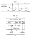
- FIG. 9 is a diagram illustrating a passing and no passing pattern between load instructions and between store instructions, which is to be assured by the TSO.
- the preceding load instruction can not be passed to process the load instruction.
- the preceding load instruction can not be passed to process the store instruction.
- the preceding store instruction can be passed to process the load instruction.
- the preceding store instruction can not be passed to process the store instruction.
- the preceding store instruction can be passed to process the load instruction, but other passing patterns are inhibited.
- a target data of the load instruction is included in a target data of the preceding store instruction, it is necessary for the load instruction to load the data of the preceding store instruction.
- the preceding load instruction can be passed to process the subsequent load instruction, and the data can be returned before the processing of the preceding load instruction to an instruction control unit as follow.
- FIG. 10 is a diagram for describing an example of the passing between the load instructions in the processor which executes an out-of-order processing.
- an instruction control unit 100 issues an load instruction load-A to a cache control unit 200.
- the cache control unit 200 requests the corresponding data to an external storage means.
- the instruction control unit 100 issues a load instruction load-B to the cache control unit 200.
- the cache control unit 200 passes a processing of the preceding load instruction load-A, executes a processing of the subsequent load instruction load-B, and returns data-B, which is the target data of the load instruction load-B, to the instruction control unit 100.
- the cache control unit 200 executes the processing of the load instruction load-A, and returns data-A, which is the target data of the load instruction load-A, to the instruction control unit 100.
- the SMT is technique for simultaneously executing the plurality of threads on a single CPU.
- the SMT processor is the processor provided with a function for simultaneously executing the plurality of threads.
- Patent Document 1 which describes the prior art for the SMT processor.
- the Patent Document 1 describes that consistency of execution order is assured for the reading and the writing of shared data between the threads.
- Patent Document 1 WO2004/068361
- FIGS. 11 to 13 are diagrams for describing examples of TSO infringement in an SMT structure.
- a memory access request such as the load instruction and the store instruction is issued from an instruction control unit 100 to a primary cache control unit 200, and is temporarily held in an FP (Fetch Port) 220, which includes a plurality of entries.
- FP Fetch Port
- the instructions issued from the instruction control unit 100 are cyclically assigned to the entry of the FP 220 according to execution order of the instructions.
- a request held in the FP 220 is read out of order, and target data of the request can be returned from the request, which is read and is to be able to process, to the instruction control unit 100.
- the store-A and the store-B issued in the thread- ⁇ are held in a FP 220 ⁇ in order of the store-A and the store-B.
- the load-B and the load-A issued in the thread- ⁇ are held in a FP 220 ⁇ in order of the load-B and the load-A.
- a number which is indicated in a left side of the instruction held in each FP 220 denotes a number for indicating each entry.
- the primary cache control unit 200 it is assumed that the instruction issued in the thread- ⁇ is firstly processed. Then, the area B of the cache RAM 210 is accessed by the preceding load-B in the thread- ⁇ . But, data of the area B does not exist in the cache RAM 210, so that a cache miss occurs on the data. Thus, the data of the load-B is requested to a secondary cache control unit 300.
- the area A of the cache RAM 210 is accessed by the subsequent load-A.
- a cache hit occurs on the data, and obtained data-A (old) is returned to the instruction control unit 100.
- FIG. 11 to 13 such a fact that the data of the area A is described as "old" indicates that the data of the area A is older as compared with the data rewritten by the processing of the subsequent store-A.
- the data of the area B which is transferred from the secondary cache control unit 300, arrives at the cache RAM 210.
- the instruction issued in the thread- ⁇ is first processed in the primary cache control unit 200 before the load-B of the thread- ⁇ is reprocessed.
- the area A and the area B of the cache RAM 210 are accessed by the store-A and the store-B.
- a cache hit occurs on both of the data of the store-A and the store-B, and both of the data of the store-A and the store-B of the cache RAM 210 is updated.
- the load-B of the thread- ⁇ is reprocessed in the primary cache control unit 200.
- the area B of the cache RAM 210 is accessed by the load-B, a cache hit occurs on the data, and obtained data-B (new) is returned to the instruction control unit 100 (refer to FIG. 13 ).
- an SMT processor for simultaneously executing a plurality of threads employs the following.
- processing of a subsequent load instruction is executed in one thread before processing of a preceding load instruction and target data of the subsequent load instruction is returned before the processing of the preceding load instruction to an instruction control unit, the execution of storage processing for the target data by another thread may cause the TSO infringement. Therefore, when the preceding load instruction is processed, the instruction control unit is requested to re-execute instructions from next instruction of the preceding load instruction to the above subsequent load instruction, and then the TSO infringement is avoided.
- each entry of an FP for each thread is provided with a flag indicating that processing is completed and a flag indicating that it is necessary to re-execute the instruction because of the storage processing in another thread, and each FP of each thread is provided with information indicating an entry which holds the oldest request.
- an entry in another thread ⁇ is extracted which has a target address corresponds to a target address in the executed storage processing and holds a load type instruction whose processing is completed. And, when the entry is extracted, a flag is set indicating that re-execution of the instruction is needed due to the storage processing of another thread for all the entries from a first entry to a second entry.
- the first entry is an entry which holds the oldest request of the FP of the thread ⁇ , or the next entry.
- the second entry is an entry which has the target address corresponds to the target address in the executed storage processing and holds the processing-completed load type instruction.
- the re-execution request of the instruction is issued to the instruction control unit.
- an information processing apparatus includes an instruction control unit, a cache control unit, a processing unit, a determination circuit, and an instruction re-execution request circuit.
- the instruction control unit controls a plurality of threads, each of the plurality of threads being a sequence of instructions.
- the cache control unit includes a cache memory.
- the processing unit processes instructions out of order, and executing the plurality of threads simultaneously, and the instructions include store instructions for memory access and load instructions for memory access.
- the determination circuit is provided in the cache control unit, and determines, when a store instruction to the cache memory is executed by a first thread, whether or not a second thread including a first load instruction and a second load instruction executes the second load instruction before the first load instruction and a target data of the second load instruction is returned to the instruction control unit before the store instruction is executed, and the first load instruction precedes the second load instruction, and the second load instruction loads data of a target address of the store instruction.
- the instruction re-execution request circuit is provided in the cache control unit, and requests, when the determination circuit determines that the target data of the second load instruction is returned to the instruction control unit before the store instruction is executed, the instruction control unit to re-execute instructions from a next instruction of the first load instruction to the second load instruction at a time of processing the first load instruction.
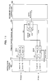
- FIG. 1 is a diagram illustrating an exemplary structure of a processor of the present embodiment.
- a CPU 1 is an SMT processor which can execute a plurality of threads simultaneously or in parallel, and is provided with an instruction control unit 10, a primary cache control unit 20, and a secondary cache control unit 30.
- the primary cache control unit 20 is provided with a cache RAM 21, an FP (Fetch Port) 22, an FP-TOQ (Fetch Port Top Of Queue) 23, a store control unit 24, an address correspondence determination circuit 25, and an instruction re-execution request circuit 26.
- a structure of the primary cache control unit 20 of FIG. 1 is illustrated only parts related to the present embodiments.
- a thread is a sequence of instructions which is executed successively in the CPU 1.
- the instruction control unit 10 issues a request such as a load instruction and a store instruction to the primary cache control unit 20.
- the primary cache control unit 20 executes processing in response to a request from the instruction control unit 10.
- the primary cache control unit 20 requests the secondary cache control unit 30 to transfer the corresponding data.
- the request from the instruction control unit 10 is a load instruction
- the primary cache control unit 20 returns the data to the instruction control unit 10.
- the secondary cache control unit 30 receives the request of data transfer from the primary cache control unit 20, and then confirms whether the data requested from the primary cache control unit 20 exists in a cache RAM provided in the secondary cache control unit 30. When the requested data exists, the secondary cache control unit 30 returns the requested data to the primary cache control unit 20. When the data requested from the primary cache control unit 20 does not exist, the secondary cache control unit 30 requests external storage means to transfer the corresponding data.
- the cache RAM 21 is storage means with a small capacity and a fast access.
- the FP 22 includes a plurality of entries which hold the requests received from the instruction control unit 10. Each entry of the FP 22 is provided with a store-initiated instruction re-execution request flag (RIS: ReIfetch for Store).
- RIS ReIfetch for Store
- the instruction issued from the instruction control unit 10 is cyclically assigned to the plurality of entries of the FP 22 according to execution order of the instruction.
- the requests held in the FP 22 are read out of order, and target data of the read request which can be processed may be returned to the instruction control unit 10.
- the FP 22 is provided for each parallel-executed thread.
- the FP-TOQ 23 is a register which holds information indicating an entry which holds the oldest request among the entries of the FP 22.
- the FP-TOQ 23 is provided for each parallel-executed thread like the FP 22.
- a release timing of the request held in the FP 22 is a processing completion time of the request held in the entry indicated by the FP-TOQ 23.
- processing of the request held in the entry, which is not indicated by the FP-TOQ 23 is completed before the processing of the preceding load instruction by passing processing of the request held in the entry indicated by the FP-TOQ 23.
- the request which is processed before the processing of the preceding load instruction is continued to be held in the FP 22 as being indicated to be in a completion status.
- the processing-completed entries are collectively released.
- the store control unit 24 When the data on the cache RAM 21 is rewritten by the store instruction, the store control unit 24 notifies the address correspondence determination circuit 25 of a target address of the store instruction.
- the address correspondence determination circuit 25 receives the target address of the store instruction from the store control unit 24, and searches the FP 22 of the thread other than the thread to which the store instruction belongs. As a result of the search, when the request is detected which is a load instruction, whose processing is completed, and whose target address corresponds to the received address, the address correspondence determination circuit 25 sets the store-initiated instruction re-execution request flag. This flag is set to all entries from an entry indicated by the FP-TOQ 23 or an entry next to the entry indicated by the FP-TOQ 23 to the entry which holds the detected request. The address correspondence determination circuit 25 may set the store-initiated instruction re-execution request flag to only an entry which holds the detected request.
- the instruction re-execution request circuit 26 transfers the re-execution request of the instruction to the instruction control unit 10 for the request held in the entry in which the store-initiated instruction re-execution request flag is set.
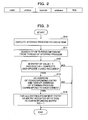
- FIG. 2 is a diagram illustrating an example of structure elements of information which is held in the entry of the FP.
- the example of FIG. 2 illustrates a structure of parts particularly related to the present embodiment of the information held in the entry of the FP 22.
- Each entry of the FP 22 includes information such as a flag "valid", a flag "status”, an instruction code (opcode), "address”, and the above store-initiated instruction re-execution request flag (RIS).
- the flag "valid” indicates whether the entry is released or not, in other words, whether the held request is invalid or valid.
- the flag "status” indicates whether the processing of the held request is completed, or is not completed.
- the instruction code (opcode) indicates a type of the instruction such as the load instruction and the store instruction.
- the "address” is a target of the instruction.
- FIG. 3 is a setting processing flowchart of the store-initiated instruction re-execution request flag of the present embodiment.
- step S12 Yes When the entry, in which the "valid” is “1”, the "status” is "complete”, and the "opcode” is the load type instruction, exists in the searched FP 22 (step S12 Yes), and when the "address" of the entry and the target address in the executed storage processing correspond to each other (step S13 Yes), the store-initiated instruction re-execution request flag (RIS) is set to all the entries from a next entry of the entry indicated by the FP-TOQ23 to the corresponding entry (step S14).
- RIS store-initiated instruction re-execution request flag
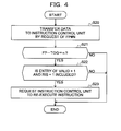
- FIG. 4 is an instruction re-execution request processing flowchart of the present embodiment.
- the data is transferred to the instruction control unit 10 by the request held in the entry FP#n (step S20). Then, when the entry FP#n is the entry indicated by the FP-TOQ23 (step S21 Yes), and when the entry, in which the "valid” is "1", and the instruction re-execution request flag (RIS) is "1", exists in the FP 22 of the thread including the entry FP#n (step S22 Yes), the instruction control unit 10 is requested to re-execute the instruction for all the requests held in the corresponding entry (step S23).
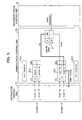
- FIGS. 5 to 8 are diagrams for describing examples of TSO infringement avoidance of an SMT structure.
- a memory access request such as the load instruction and the store instruction, which is issued from the instruction control unit 10 to the primary cache control unit 20, is temporarily held in the FP 22.
- the number of the threads in the processor is "2"
- the FP 22 is provided for each thread.
- the store-A is held in the 0-th entry (hereinafter, described as FP ⁇ #0) of FP22 ⁇
- the store-B is held in the 1-th entry (hereinafter, described as FP ⁇ #1) of FP22 ⁇
- FP-TOQ23 ⁇ of the FP22 ⁇ indicates the entry FP ⁇ #0.
- the load-B is held in the 0-th entry (hereinafter, described as FP ⁇ #0) of FP22 ⁇
- the load-A is held in the 1-th entry (hereinafter, described as FP ⁇ #1) of FP22 ⁇
- FP-TOQ23 ⁇ of the FP22 ⁇ indicates the entry FP ⁇ #0 (refer to FIG. 5 ).
- a number indicated in a left side of the instruction held in each FP 22 denotes a number for indicating each entry.
- the request is first issued from which of the FP22 ⁇ and the FP22 ⁇ , and the request held in which entry is first processed in the FP22 ⁇ and the FP22 ⁇ .
- the request held in the entry is processed in order of the FP ⁇ #0, the FP ⁇ #1, the FP ⁇ #0, and the FP ⁇ #1.
- the primary cache control unit 20 firstly executes processing of the load-B held in the FP ⁇ #0. However, data does not exist in the area B of the cache RAM 21, so that a cache miss occurs on the data. Then, the primary cache control unit 20 requests the secondary cache control unit 30 or a main memory (not-illustrated) to transfer the data (refer to FIG. 5 ).
- the processing of the store-A held in the FP ⁇ #0 of the thread- ⁇ is executed, and the data is written in the area A of the cache RAM 21.
- the addresses of all the processing-completed requests are checked which are held in the FP22 of the thread other than the thread- ⁇ . In this case, the addresses of the FP22 ⁇ of the thread- ⁇ are checked.
- the store-initiated instruction re-execution request flag (RIS) is set to all entries from an entry indicated by the FP-TOQ23 ⁇ of the FP22 ⁇ or an entry next to the entry indicated by the FP-TOQ23 ⁇ of the FP22 ⁇ to the corresponding entry.
- the entry FP ⁇ #1 which holds the request of the address corresponding to the area-A exists, so that the store-initiated instruction re-execution request flag (RIS) is set to the entries from the FP ⁇ #0 indicated by the FP-TOQ23 ⁇ of the FP22 ⁇ to the FP ⁇ #1, or set to only the entry FP ⁇ #1 (refer to FIG. 6 ).
- "1" is set to the RIS of the entry of the FP ⁇ #1.
- the data including the area B arrives at the primary cache control unit 20 from the secondary cache control unit 30, and is written in the area B of the cache RAM 21.
- the processing of the store-B held in the FP ⁇ #1 of the thread- ⁇ is executed, and the data is written in the area B of the cache RAM 21 (refer to FIG. 6 ).
- FIGS. 5 to 8 such a fact that the data of the area A and the area B is described as "new" indicates that such data is newer as compared with the data before rewriting by the processing of the store-A and the store-B.
- the re-processing of the load-B held in the FP ⁇ #0 of the thread- ⁇ is executed, and a cache hit occurs on the data.
- the data of the area B of the cache RAM 21 is read, and the obtained data-B (new) is returned to the instruction control unit 10.
- the FP ⁇ #0 is the entry indicated by the FP-TOQ23 ⁇ .
- the re-execution request of the instruction is issued to the instruction control unit 10 (refer to FIG. 7 ).
- the load-A is again requested as the thread- ⁇ from the instruction control unit 10, and the request is held in the second entry (hereinafter, described as FP ⁇ #2) of the FP22 ⁇ . Then, processing of the load-A held in the FP ⁇ #2 is executed, and a cache hit occurs on the data.
- the data of the area A of the cache RAM 21 is read, and the obtain data-A (new) is returned to the instruction control unit 10 (refer to FIG. 8 ). Thereby, the stored data by the processing of the store-A of the thread- ⁇ is returned to the instruction control unit 10.
- This state seems from software that the processing order of the store-A and the store-B of the thread- ⁇ is reversed, so that it results in the TSO infringement. Since the store-initiated instruction re-execution is executed, the stored data of the thread- ⁇ is returned in the processing of both the load-A and the load-B of the thread- ⁇ , so that the TSO infringement can be avoided.
- the information processing apparatus, the cache memory controlling apparatus, and the memory access order assuring method are related to the technique used by the information processing apparatus, and particularly, to the technique used by a computer including a cache.
Landscapes
- Engineering & Computer Science (AREA)
- Theoretical Computer Science (AREA)
- Software Systems (AREA)
- Physics & Mathematics (AREA)
- General Engineering & Computer Science (AREA)
- General Physics & Mathematics (AREA)
- Multimedia (AREA)
- Memory System Of A Hierarchy Structure (AREA)
- Advance Control (AREA)
Abstract
Description
- The embodiments discussed herein are related to an information processing apparatus, a cache memory controlling apparatus, and a memory access order assuring method.
- The TSO (Total Store Ordering) is one type of memory ordering. The TSO has limitations for changing writing order in which data is actually written into a memory with respect to order of instructions which access the memory. There are three TSO rules:
- 1. A load instruction can not pass a preceding load instruction, which precedes the load instruction, to process the load instruction;
- 2. A store instruction can not pass a preceding load instruction and the preceding store instruction, both of which precedes the store instruction, to process the store instruction; and
- 3. An atomic load store instruction can not pass a preceding load instruction and the preceding store instruction, both of which precedes the atomic load store instruction, to process the atomic load store instruction. When a target data is loaded by the atomic load store instruction, an access to the target data from another instruction is restricted from a time the target data is loaded until a time the target data is stored by the atomic load store instruction.
-
FIG. 9 is a diagram illustrating a passing and no passing pattern between load instructions and between store instructions, which is to be assured by the TSO. As illustrated in #1, the preceding load instruction can not be passed to process the load instruction. As illustrated in #2, the preceding load instruction can not be passed to process the store instruction. As illustrated in #3, the preceding store instruction can be passed to process the load instruction. As illustrated in #4, the preceding store instruction can not be passed to process the store instruction. - In other words, the preceding store instruction can be passed to process the load instruction, but other passing patterns are inhibited. However, when a target data of the load instruction is included in a target data of the preceding store instruction, it is necessary for the load instruction to load the data of the preceding store instruction.
- Here, in a processor which processes a memory access out of order, the preceding load instruction can be passed to process the subsequent load instruction, and the data can be returned before the processing of the preceding load instruction to an instruction control unit as follow.
-
FIG. 10 is a diagram for describing an example of the passing between the load instructions in the processor which executes an out-of-order processing. In the processor which executes the out-of-order processing, aninstruction control unit 100 issues an load instruction load-A to acache control unit 200. When a cache miss occurs on a target data of the load instruction load-A, thecache control unit 200 requests the corresponding data to an external storage means. - Next, the
instruction control unit 100 issues a load instruction load-B to thecache control unit 200. When a cache hit occurs on a target data of the load instruction load-B, thecache control unit 200 passes a processing of the preceding load instruction load-A, executes a processing of the subsequent load instruction load-B, and returns data-B, which is the target data of the load instruction load-B, to theinstruction control unit 100. - After that, when receiving transferred data from the external storage means, the
cache control unit 200 executes the processing of the load instruction load-A, and returns data-A, which is the target data of the load instruction load-A, to theinstruction control unit 100. - As described above, in the out-of-order processing, data is not always read from a cache in order of the instructions. However, the instructions are actually executed by the
instruction control unit 100 in order of the instructions. Thus, in a processor which supports only single thread, even when the data is read out of order, as long as the TSO between the load/store instructions is observed, it seems from software that the TSO is observed. - However, in an SMT (Simultaneous Multi Thread) processor, a plurality of threads which are simultaneously executed share a primary cache. Then, it becomes necessary to avoid a TSO infringement between the threads in single processor.
- The SMT is technique for simultaneously executing the plurality of threads on a single CPU. In other words, the SMT processor is the processor provided with a function for simultaneously executing the plurality of threads. There is a
Patent Document 1 which describes the prior art for the SMT processor. ThePatent Document 1 describes that consistency of execution order is assured for the reading and the writing of shared data between the threads. - Patent Document 1:
WO2004/068361 -
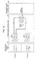
FIGS. 11 to 13 are diagrams for describing examples of TSO infringement in an SMT structure. In the examples illustrated inFIGS. 11 to 13 , a memory access request such as the load instruction and the store instruction is issued from aninstruction control unit 100 to a primarycache control unit 200, and is temporarily held in an FP (Fetch Port) 220, which includes a plurality of entries. Here, it is assumed for convenience of the description that the number of the threads in the processor is "2", and the FP 220 is provided in each thread. The instructions issued from theinstruction control unit 100 are cyclically assigned to the entry of theFP 220 according to execution order of the instructions. A request held in theFP 220 is read out of order, and target data of the request can be returned from the request, which is read and is to be able to process, to theinstruction control unit 100. - Here, a following case is described. That is, there are an area A in which the data does not exist, and an area B in which the data exists, on the
cache RAM 210. One thread (thread-α) in a processor issues instructions from theinstruction control unit 100 to the primarycache control unit 200 in order of store-A and store-B for the area A and area B. And, another thread (thread-β) in the processor issues instructions from theinstruction control unit 100 to the primarycache control unit 200 in order of load-B and load-A for the area B and the area A (refer toFIG. 11 ). - The store-A and the store-B issued in the thread-α are held in a FP 220α in order of the store-A and the store-B. And, the load-B and the load-A issued in the thread-β are held in a FP 220β in order of the load-B and the load-A. In
FIGS. 11 to 13 , a number which is indicated in a left side of the instruction held in eachFP 220 denotes a number for indicating each entry. - In the primary
cache control unit 200, it is assumed that the instruction issued in the thread-β is firstly processed. Then, the area B of thecache RAM 210 is accessed by the preceding load-B in the thread-β. But, data of the area B does not exist in thecache RAM 210, so that a cache miss occurs on the data. Thus, the data of the load-B is requested to a secondarycache control unit 300. - While the target data of the load-B is requested to the secondary
cache control unit 300, the area A of thecache RAM 210 is accessed by the subsequent load-A. In this case, a cache hit occurs on the data, and obtained data-A (old) is returned to theinstruction control unit 100. InFIG. 11 to 13 , such a fact that the data of the area A is described as "old" indicates that the data of the area A is older as compared with the data rewritten by the processing of the subsequent store-A. - After that, as illustrated in
FIG. 12 , the data of the area B, which is transferred from the secondarycache control unit 300, arrives at thecache RAM 210. Here, it is assumed that the instruction issued in the thread-α is first processed in the primarycache control unit 200 before the load-B of the thread-β is reprocessed. The area A and the area B of thecache RAM 210 are accessed by the store-A and the store-B. In this case, a cache hit occurs on both of the data of the store-A and the store-B, and both of the data of the store-A and the store-B of thecache RAM 210 is updated. InFIGS. 11 to 13 , such a fact that the data of the area A and the area B are described as "new" indicates that the data of the area A and the area B are newer as compared with the data which are not rewritten by the processing of the store-A and the store-B. - After that, the load-B of the thread-β is reprocessed in the primary
cache control unit 200. When the area B of thecache RAM 210 is accessed by the load-B, a cache hit occurs on the data, and obtained data-B (new) is returned to the instruction control unit 100 (refer toFIG. 13 ). - As a result, although the instructions are issued in order of the store-A and the store-B in the thread-α, in the thread-β, the stored data is returned in the processing of the load-B, and the pre-stored data is returned in the processing of the load-A. Thus, passing prohibition is infringed between the load instructions in the TSO.
- It is an object of the present invention to provide a technique to solve the above problem, and to assure in the SMT processor for processing a memory access out of order that the order of store processing executed in one thread is reflected to loading processes executed in another thread in the same processor.
- To solve the above problem, an SMT processor for simultaneously executing a plurality of threads employs the following. When processing of a subsequent load instruction is executed in one thread before processing of a preceding load instruction and target data of the subsequent load instruction is returned before the processing of the preceding load instruction to an instruction control unit, the execution of storage processing for the target data by another thread may cause the TSO infringement. Therefore, when the preceding load instruction is processed, the instruction control unit is requested to re-execute instructions from next instruction of the preceding load instruction to the above subsequent load instruction, and then the TSO infringement is avoided.
- In a cache control unit of the SMT processor for simultaneously executing a plurality of threads, each entry of an FP for each thread is provided with a flag indicating that processing is completed and a flag indicating that it is necessary to re-execute the instruction because of the storage processing in another thread, and each FP of each thread is provided with information indicating an entry which holds the oldest request.
- When storage processing is executed in one thread α, an entry in another thread β is extracted which has a target address corresponds to a target address in the executed storage processing and holds a load type instruction whose processing is completed. And, when the entry is extracted, a flag is set indicating that re-execution of the instruction is needed due to the storage processing of another thread for all the entries from a first entry to a second entry. The first entry is an entry which holds the oldest request of the FP of the thread β, or the next entry. The second entry is an entry which has the target address corresponds to the target address in the executed storage processing and holds the processing-completed load type instruction.
- When the oldest request of the FP of the thread β is executed, for an instruction held in the entry in which the flag is set indicating that re-execution of the instruction is needed due to the storage processing of another thread, the re-execution request of the instruction is issued to the instruction control unit.
- According to an aspect of the embodiment, an information processing apparatus includes an instruction control unit, a cache control unit, a processing unit, a determination circuit, and an instruction re-execution request circuit. The instruction control unit controls a plurality of threads, each of the plurality of threads being a sequence of instructions. The cache control unit includes a cache memory. The processing unit processes instructions out of order, and executing the plurality of threads simultaneously, and the instructions include store instructions for memory access and load instructions for memory access. The determination circuit is provided in the cache control unit, and determines, when a store instruction to the cache memory is executed by a first thread, whether or not a second thread including a first load instruction and a second load instruction executes the second load instruction before the first load instruction and a target data of the second load instruction is returned to the instruction control unit before the store instruction is executed, and the first load instruction precedes the second load instruction, and the second load instruction loads data of a target address of the store instruction. The instruction re-execution request circuit is provided in the cache control unit, and requests, when the determination circuit determines that the target data of the second load instruction is returned to the instruction control unit before the store instruction is executed, the instruction control unit to re-execute instructions from a next instruction of the first load instruction to the second load instruction at a time of processing the first load instruction.
- According to the embodiment, in the SMT processor which processes the memory access out of order, order of data update between the threads is assured.
-
-
FIG. 1 is a diagram illustrating an exemplary structure of a processor of the present embodiment; -
FIG. 2 is a diagram illustrating an example of structure elements of information held in an entry of an FP; -
FIG. 3 is a setting processing flowchart of a store-initiated instruction re-execution request flag of the present embodiment; -
FIG. 4 is an instruction re-execution request processing flowchart of the present embodiment; -
FIG. 5 is a diagram for describing an example of TSO infringement avoidance of an SMT structure; -
FIG. 6 is a diagram for describing an example of the TSO infringement avoidance of the SMT structure; -
FIG. 7 is a diagram for describing an example of the TSO infringement avoidance of the SMT structure; -
FIG. 8 is a diagram for describing an example of the TSO infringement avoidance of the SMT structure; -
FIG. 9 is a diagram illustrating passing and no passing pattern between a load instruction and a store instruction to be assured by TSO; -
FIG. 10 is a diagram for describing an example of the passing between the load instructions in a processor which executes an out-of-order processing; -
FIG. 11 is a diagram for describing an example of TSO infringement of the SMT structure; -
FIG. 12 is a diagram for describing an example of the TSO infringement of the SMT structure; and -
FIG. 13 is a diagram for describing an example of the TSO infringement of the SMT structure. - Preferred embodiments of the present invention will be explained with reference to accompanying drawings.
-
FIG. 1 is a diagram illustrating an exemplary structure of a processor of the present embodiment. ACPU 1 is an SMT processor which can execute a plurality of threads simultaneously or in parallel, and is provided with aninstruction control unit 10, a primarycache control unit 20, and a secondarycache control unit 30. The primarycache control unit 20 is provided with acache RAM 21, an FP (Fetch Port) 22, an FP-TOQ (Fetch Port Top Of Queue) 23, astore control unit 24, an addresscorrespondence determination circuit 25, and an instructionre-execution request circuit 26. A structure of the primarycache control unit 20 ofFIG. 1 is illustrated only parts related to the present embodiments. A thread is a sequence of instructions which is executed successively in theCPU 1. - The
instruction control unit 10 issues a request such as a load instruction and a store instruction to the primarycache control unit 20. The primarycache control unit 20 executes processing in response to a request from theinstruction control unit 10. When data which is a target of the request from theinstruction control unit 10 does not exist in thecache RAM 21, the primarycache control unit 20 requests the secondarycache control unit 30 to transfer the corresponding data. When the request from theinstruction control unit 10 is a load instruction, the primarycache control unit 20 returns the data to theinstruction control unit 10. - The secondary
cache control unit 30 receives the request of data transfer from the primarycache control unit 20, and then confirms whether the data requested from the primarycache control unit 20 exists in a cache RAM provided in the secondarycache control unit 30. When the requested data exists, the secondarycache control unit 30 returns the requested data to the primarycache control unit 20. When the data requested from the primarycache control unit 20 does not exist, the secondarycache control unit 30 requests external storage means to transfer the corresponding data. - In the primary
cache control unit 20, thecache RAM 21 is storage means with a small capacity and a fast access. - The
FP 22 includes a plurality of entries which hold the requests received from theinstruction control unit 10. Each entry of theFP 22 is provided with a store-initiated instruction re-execution request flag (RIS: ReIfetch for Store). The instruction issued from theinstruction control unit 10 is cyclically assigned to the plurality of entries of theFP 22 according to execution order of the instruction. The requests held in theFP 22 are read out of order, and target data of the read request which can be processed may be returned to theinstruction control unit 10. TheFP 22 is provided for each parallel-executed thread. - The FP-
TOQ 23 is a register which holds information indicating an entry which holds the oldest request among the entries of theFP 22. The FP-TOQ 23 is provided for each parallel-executed thread like theFP 22. - A release timing of the request held in the
FP 22 is a processing completion time of the request held in the entry indicated by the FP-TOQ 23. There is a case that processing of the request held in the entry, which is not indicated by the FP-TOQ 23, is completed before the processing of the preceding load instruction by passing processing of the request held in the entry indicated by the FP-TOQ 23. In this case, the request which is processed before the processing of the preceding load instruction is continued to be held in theFP 22 as being indicated to be in a completion status. After that, at the time point that the request held in the entry indicated by the FP-TOQ 23 is completed, the processing-completed entries are collectively released. - When the data on the
cache RAM 21 is rewritten by the store instruction, thestore control unit 24 notifies the addresscorrespondence determination circuit 25 of a target address of the store instruction. - The address
correspondence determination circuit 25 receives the target address of the store instruction from thestore control unit 24, and searches theFP 22 of the thread other than the thread to which the store instruction belongs. As a result of the search, when the request is detected which is a load instruction, whose processing is completed, and whose target address corresponds to the received address, the addresscorrespondence determination circuit 25 sets the store-initiated instruction re-execution request flag. This flag is set to all entries from an entry indicated by the FP-TOQ 23 or an entry next to the entry indicated by the FP-TOQ 23 to the entry which holds the detected request. The addresscorrespondence determination circuit 25 may set the store-initiated instruction re-execution request flag to only an entry which holds the detected request. - When processing of the request held in the entry indicated by the FP-
TOQ 23 is executed, the instructionre-execution request circuit 26 transfers the re-execution request of the instruction to theinstruction control unit 10 for the request held in the entry in which the store-initiated instruction re-execution request flag is set. -
FIG. 2 is a diagram illustrating an example of structure elements of information which is held in the entry of the FP. The example ofFIG. 2 illustrates a structure of parts particularly related to the present embodiment of the information held in the entry of theFP 22. Each entry of theFP 22 includes information such as a flag "valid", a flag "status", an instruction code (opcode), "address", and the above store-initiated instruction re-execution request flag (RIS). The flag "valid" indicates whether the entry is released or not, in other words, whether the held request is invalid or valid. The flag "status" indicates whether the processing of the held request is completed, or is not completed. The instruction code (opcode) indicates a type of the instruction such as the load instruction and the store instruction. The "address" is a target of the instruction. - In the present embodiment, it is assumed that the "valid" becomes "0" when the held request is invalid, and becomes "1" when the held request is valid. It is assumed that the "status" becomes "incomplete" when the processing of the held request is not completed, and becomes "complete" when the processing of the held request is completed. It is assumed that the store-initiated instruction re-execution request flag is "0" in the case of default, and becomes "1" in the case of flag set.
-
FIG. 3 is a setting processing flowchart of the store-initiated instruction re-execution request flag of the present embodiment. When storage processing to thecache RAM 21 is executed (step S10), theFP 22 of the thread is searched which is different from the thread in which the storage processing is executed (step S11). - When an entry, in which the "valid" is "1", the "status" is "complete", and the "opcode" is the load type instruction, does not exist in the searched FP 22 (step S12 No), the store-initiated instruction re-execution request flag (RIS) is not set.
- When the entry, in which the "valid" is "1", the "status" is "complete", and the "opcode" is the load type instruction, exists in the searched FP 22 (step S12 Yes), and when the "address" of the entry and the target address in the executed storage processing correspond to each other (step S13 Yes), the store-initiated instruction re-execution request flag (RIS) is set to all the entries from a next entry of the entry indicated by the FP-TOQ23 to the corresponding entry (step S14).
- Even when the entry, in which the "valid" is "1", the "status" is "complete", and the "opcode" is the load type instruction, exists in the searched FP 22 (step S12 Yes), and when the "address" of the entry and the target address in the executed storage processing does not correspond to each other (step S13 No), the store-initiated instruction reexecution request flag (RIS) is not set.
-
FIG. 4 is an instruction re-execution request processing flowchart of the present embodiment. In the flowchart ofFIG. 4 , FP#n (n = 0, 1, 2, ...) indicates each entry of theFP 22, and n (n = 0, 1, 2, ...) indicates a number which is conveniently assigned to the entry. - The data is transferred to the
instruction control unit 10 by the request held in the entry FP#n (step S20). Then, when the entry FP#n is the entry indicated by the FP-TOQ23 (step S21 Yes), and when the entry, in which the "valid" is "1", and the instruction re-execution request flag (RIS) is "1", exists in theFP 22 of the thread including the entry FP#n (step S22 Yes), theinstruction control unit 10 is requested to re-execute the instruction for all the requests held in the corresponding entry (step S23). -
FIGS. 5 to 8 are diagrams for describing examples of TSO infringement avoidance of an SMT structure. Here, more particular example of the processing performed by the primarycache control unit 20 of the present embodiment is described by usingFIGS. 5 to 8 . In the examples illustrated inFIGS. 5 to 8 , a memory access request such as the load instruction and the store instruction, which is issued from theinstruction control unit 10 to the primarycache control unit 20, is temporarily held in theFP 22. Here, it is assumed for convenience of the description that the number of the threads in the processor is "2", and theFP 22 is provided for each thread. - In the examples illustrated in
FIGS. 5 to 8 , such a case is described that, for an area A in which the data does not exist on thecache RAM 21 and an area B in which the data exists on thecache RAM 21, requests are executed in order of store-A and store-B in a thread-α, and requests are executed in order of load-B and load-A in a thread-β (refer toFIG. 5 ). - It is assumed that, with regard to instructions issued from the
instruction control unit 10 in the thread-α, the store-A is held in the 0-th entry (hereinafter, described as FPα#0) of FP22α, the store-B is held in the 1-th entry (hereinafter, described as FPα#1) of FP22α, and FP-TOQ23α of the FP22α indicates theentry FPα# 0. It is assumed that, with regard to the instruction issued from theinstruction control unit 10 in the thread-β, the load-B is held in the 0-th entry (hereinafter, described as FPβ#0) of FP22β, the load-A is held in the 1-th entry (hereinafter, described as FPβ#1) of FP22β, and FP-TOQ23β of the FP22β indicates the entry FPβ#0 (refer toFIG. 5 ). InFIGS. 5 to 8 , a number indicated in a left side of the instruction held in eachFP 22 denotes a number for indicating each entry. - It is basically in random order that the request is first issued from which of the FP22α and the FP22β, and the request held in which entry is first processed in the FP22α and the FP22β. Here, it is assumed that the request held in the entry is processed in order of the
FPβ# 0, theFPβ# 1, theFPα# 0, and theFPα# 1. - The primary
cache control unit 20 firstly executes processing of the load-B held in theFPβ# 0. However, data does not exist in the area B of thecache RAM 21, so that a cache miss occurs on the data. Then, the primarycache control unit 20 requests the secondarycache control unit 30 or a main memory (not-illustrated) to transfer the data (refer toFIG. 5 ). - By the time that the requested data arrives at the
cache RAM 21, the processing of the load-A held in theFPβ# 1 is started, and a cache hit occurs on the data. Thus, the data of the area A of thecache RAM 21 is read, and the obtained data-A (old) is returned to the instruction control unit 10 (refer toFIG. 5 ). At this time point, in the thread-β, the processing of the load-A passes the processing of the load-B, and returns the data to theinstruction control unit 10. InFIGS. 5 to 8 , such a fact that the data of the area A is described as "old" in the diagram indicates that such a data is older as compared with the data rewritten by the subsequent processing of the store-A. - And, at this time point, the processing of the load-A held in the
FPβ# 1 is completed, but the processing of the load-B held in theFPβ# 0 indicated by the FP-TOQ23β is not completed. Accordingly, at this time point, the flag of the processing completion is set to theFPβ# 1, but theFPβ# 1 is not released. - After that, the processing of the store-A held in the
FPα# 0 of the thread-α is executed, and the data is written in the area A of thecache RAM 21. When the data is written for this store-A, the addresses of all the processing-completed requests are checked which are held in the FP22 of the thread other than the thread-α. In this case, the addresses of the FP22β of the thread-β are checked. And, when an entry which holds the request of the address corresponding to the area A exists, the store-initiated instruction re-execution request flag (RIS) is set to all entries from an entry indicated by the FP-TOQ23β of the FP22β or an entry next to the entry indicated by the FP-TOQ23β of the FP22β to the corresponding entry. In this case, theentry FPβ# 1 which holds the request of the address corresponding to the area-A exists, so that the store-initiated instruction re-execution request flag (RIS) is set to the entries from theFPβ# 0 indicated by the FP-TOQ23β of the FP22β to theFPβ# 1, or set to only the entry FPβ#1 (refer toFIG. 6 ). InFIGS. 5 to 8 , "1" is set to the RIS of the entry of theFPβ# 1. - After that, the data including the area B arrives at the primary
cache control unit 20 from the secondarycache control unit 30, and is written in the area B of thecache RAM 21. The processing of the store-B held in theFPα# 1 of the thread-α is executed, and the data is written in the area B of the cache RAM 21 (refer toFIG. 6 ). InFIGS. 5 to 8 , such a fact that the data of the area A and the area B is described as "new" indicates that such data is newer as compared with the data before rewriting by the processing of the store-A and the store-B. - After that, the re-processing of the load-B held in the
FPβ# 0 of the thread-β is executed, and a cache hit occurs on the data. Then, the data of the area B of thecache RAM 21 is read, and the obtained data-B (new) is returned to theinstruction control unit 10. In this case, theFPβ# 0 is the entry indicated by the FP-TOQ23β. Thus, for the entry in which the store-initiated instruction re-execution request flag (RIS) is set, the re-execution request of the instruction is issued to the instruction control unit 10 (refer toFIG. 7 ). However, it is not needed to issue the re-execution request of the instruction forFPβ# 0 which is the entry indicated by the FP-TOQ23β. The processing of theFPβ# 0 which is the entry indicated by the FP-TOQ23β is completed, so that all the entries which holds the processing-completed request of the FP22β are released. - The load-A is again requested as the thread-β from the
instruction control unit 10, and the request is held in the second entry (hereinafter, described as FPβ#2) of the FP22β. Then, processing of the load-A held in theFPβ# 2 is executed, and a cache hit occurs on the data. Thus, the data of the area A of thecache RAM 21 is read, and the obtain data-A (new) is returned to the instruction control unit 10 (refer toFIG. 8 ). Thereby, the stored data by the processing of the store-A of the thread-α is returned to theinstruction control unit 10. - In a case that the above mechanism for the store-initiated instruction re-execution does not employed, the state in which the data returned to the
instruction control unit 10 in the processing of the load-B of the thread-β is the stored data but the data returned in the processing of the load-A is the pre-stored data. This state seems from software that the processing order of the store-A and the store-B of the thread-α is reversed, so that it results in the TSO infringement. Since the store-initiated instruction re-execution is executed, the stored data of the thread-α is returned in the processing of both the load-A and the load-B of the thread-β, so that the TSO infringement can be avoided. - The information processing apparatus, the cache memory controlling apparatus, and the memory access order assuring method are related to the technique used by the information processing apparatus, and particularly, to the technique used by a computer including a cache.
Claims (4)
- An information processing apparatus, comprising:an instruction control unit controlling a plurality of threads, each of the plurality of threads being a sequence of instructions;a cache control unit including a cache memory;a processing unit that processes instructions out of order, and executing the plurality of threads simultaneously, the instructions including store instructions for memory access and load instructions for memory access;a determination circuit that determines whether or not a second thread including a first load instruction and a second load instruction executes the second load instruction before the first load instruction and a target data of the second load instruction is returned to the instruction control unit before the store instruction is executed, the first load instruction preceding the second load instruction, the second load instruction loading data of a target address of the store instruction, when a store instruction to the cache memory is executed by a first thread; andan instruction re-execution request circuit that requests the instruction control unit to re-execute instructions from a next instruction of the first load instruction to the second load instruction at a time of processing the first load instruction when the determination unit determines that the target data of the second load instruction is returned to the instruction control unit before the store instruction is executed.
- A cache memory controlling apparatus having a cache memory, and used in an information processing apparatus that processes a memory access out of order and simultaneously executing a plurality of threads, the thread being a sequence of instructions, the cache memory controlling apparatus comprising:a determination circuit that determines whether or not a second thread including a first load instruction and a second load instruction executes the second load instruction before the first load instruction and a target data of the second load instruction is returned to the instruction control unit before the store instruction is executed, the first load instruction preceding the second load instruction, the second load instruction loading data of a target address of the store instruction, when a store instruction to the cache memory is executed by a first thread; andan instruction re-execution request circuit that requests the instruction control unit to re-execute instructions from a next instruction of the first load instruction to the second load instruction at a time of processing the first load instruction when the determination unit determines that the target data of the second load instruction is returned to the instruction control unit before the store instruction is executed.
- A cache memory controlling apparatus, comprising:a cache memory;a plurality of fetch port including a plurality of entries each of which holds an access request for the cache memory, the thread being a sequence of instructions, each of the plurality of entries including at least a status flag indicating whether or not processing of the held access request is completed, instruction type information, a target address of the instruction, and an instruction re-execution request flag initiated by issuing a store instruction;a plurality of queue registers holding information for each fetch port, the information indicating an entry which holds oldest access request among the entries of each fetch port;an address correspondence determination circuit searching the fetch port corresponding to the thread other than the thread issuing the store instruction when data on the cache memory is rewritten by the store instruction, and setting the instruction re-execution request flag initiated by the store instruction in each entry from the entry indicated by the queue register or from the next entry to the detected entry when an entry is detected, the entry including the instruction type information indicating a load type instruction , the status flag indicating processing-completed, and the access request whose target address corresponds to the received address of the store instruction; andan instruction re-execution request circuit transferring, when processing of the access request indicated by the queue register is executed, a re-execution request of an instruction for an access request held in an entry in which the instruction re-execution request flag initiated by the store instruction is set to an access requesting source from which the access request is issued.
- A memory access order assuring method between threads for assuring predetermined limitations on the order of instructions for accessing a memory in an information processing apparatus including an instruction control unit controlling a plurality of threads, each of the plurality of threads being a sequence of instructions, a cache control unit including a cache memory, a processing unit processing instructions out of order and executing the plurality of threads simultaneously, the instructions including store instructions for memory access and load instructions for memory access, the method comprising:determining whether or not a second thread including a first load instruction and a second load instruction executes the second load instruction before the first load instruction and a target data of the second load instruction is returned to the instruction control unit before the store instruction is executed, the first load instruction preceding the second load instruction, the second load instruction loading data of a target address of the store instruction, when a store instruction to the cache memory is executed by a first thread; andrequesting the instruction control unit to re-execute instructions from a next instruction of the first load instruction to the second load instruction at a time of processing the first load instruction when it is determined that the target data of the second load instruction is returned to the instruction control unit before the store instruction is executed.
Applications Claiming Priority (1)
| Application Number | Priority Date | Filing Date | Title |
|---|---|---|---|
| PCT/JP2007/062389 WO2008155829A1 (en) | 2007-06-20 | 2007-06-20 | Information processor, cache memory controller, and memory access sequence assurance method |
Publications (2)
| Publication Number | Publication Date |
|---|---|
| EP2159703A1 true EP2159703A1 (en) | 2010-03-03 |
| EP2159703A4 EP2159703A4 (en) | 2010-12-08 |
Family
ID=40155995
Family Applications (1)
| Application Number | Title | Priority Date | Filing Date |
|---|---|---|---|
| EP07767228A Withdrawn EP2159703A4 (en) | 2007-06-20 | 2007-06-20 | INFORMATION PROCESSOR, CACHE MEMORY CONTROLLER, AND MEMORY ACCESS SEQUENCE ASSURANCE METHOD |
Country Status (6)
| Country | Link |
|---|---|
| US (1) | US8103859B2 (en) |
| EP (1) | EP2159703A4 (en) |
| JP (1) | JP4983919B2 (en) |
| KR (1) | KR101084228B1 (en) |
| CN (1) | CN101689142A (en) |
| WO (1) | WO2008155829A1 (en) |
Families Citing this family (9)
| Publication number | Priority date | Publication date | Assignee | Title |
|---|---|---|---|---|
| JP5471428B2 (en) * | 2009-12-25 | 2014-04-16 | 富士通株式会社 | Information processing apparatus and cache memory control apparatus |
| JP5966759B2 (en) * | 2012-08-20 | 2016-08-10 | 富士通株式会社 | Arithmetic processing device and control method of arithmetic processing device |
| KR101993258B1 (en) | 2012-11-22 | 2019-09-27 | 삼성전자주식회사 | Register slicing circuit and system on chip including the same |
| JP6115394B2 (en) * | 2013-08-13 | 2017-04-19 | 富士通株式会社 | Arithmetic processing device and control method of arithmetic processing device |
| US9361176B2 (en) * | 2014-06-25 | 2016-06-07 | International Business Machines Corporation | Detecting the use of stale data values due to weak consistency |
| US10489158B2 (en) * | 2014-09-26 | 2019-11-26 | Intel Corporation | Processors, methods, systems, and instructions to selectively fence only persistent storage of given data relative to subsequent stores |
| JP6384380B2 (en) * | 2015-03-27 | 2018-09-05 | 富士通株式会社 | Arithmetic processing device and control method of arithmetic processing device |
| CN106527959B (en) * | 2015-09-10 | 2019-07-26 | 阿里巴巴集团控股有限公司 | Refresh the processing method and equipment of disk input output request |
| CN112445587A (en) * | 2019-08-30 | 2021-03-05 | 上海华为技术有限公司 | Task processing method and task processing device |
Family Cites Families (12)
| Publication number | Priority date | Publication date | Assignee | Title |
|---|---|---|---|---|
| US5699538A (en) * | 1994-12-09 | 1997-12-16 | International Business Machines Corporation | Efficient firm consistency support mechanisms in an out-of-order execution superscaler multiprocessor |
| US6665792B1 (en) * | 1996-11-13 | 2003-12-16 | Intel Corporation | Interface to a memory system for a processor having a replay system |
| US6772324B2 (en) * | 1997-12-17 | 2004-08-03 | Intel Corporation | Processor having multiple program counters and trace buffers outside an execution pipeline |
| US6591342B1 (en) * | 1999-12-14 | 2003-07-08 | Intel Corporation | Memory disambiguation for large instruction windows |
| US6484254B1 (en) * | 1999-12-30 | 2002-11-19 | Intel Corporation | Method, apparatus, and system for maintaining processor ordering by checking load addresses of unretired load instructions against snooping store addresses |
| JP3661614B2 (en) | 2001-07-12 | 2005-06-15 | 日本電気株式会社 | Cache memory control method and multiprocessor system |
| GB0215029D0 (en) * | 2002-06-28 | 2002-08-07 | Critical Blue Ltd | Strand based execution |
| WO2004068361A1 (en) * | 2003-01-27 | 2004-08-12 | Fujitsu Limited | Storage control device, data cache control device, central processing unit, storage device control method, data cache control method, and cache control method |
| US20050210204A1 (en) | 2003-01-27 | 2005-09-22 | Fujitsu Limited | Memory control device, data cache control device, central processing device, storage device control method, data cache control method, and cache control method |
| US6938130B2 (en) | 2003-02-13 | 2005-08-30 | Sun Microsystems Inc. | Method and apparatus for delaying interfering accesses from other threads during transactional program execution |
| US20060026371A1 (en) | 2004-07-30 | 2006-02-02 | Chrysos George Z | Method and apparatus for implementing memory order models with order vectors |
| US7516313B2 (en) * | 2004-12-29 | 2009-04-07 | Intel Corporation | Predicting contention in a processor |
-
2007
- 2007-06-20 CN CN200780053369A patent/CN101689142A/en active Pending
- 2007-06-20 KR KR1020097025129A patent/KR101084228B1/en not_active Expired - Fee Related
- 2007-06-20 WO PCT/JP2007/062389 patent/WO2008155829A1/en not_active Ceased
- 2007-06-20 JP JP2009520183A patent/JP4983919B2/en not_active Expired - Fee Related
- 2007-06-20 EP EP07767228A patent/EP2159703A4/en not_active Withdrawn
-
2009
- 2009-12-17 US US12/654,380 patent/US8103859B2/en not_active Expired - Fee Related
Also Published As
| Publication number | Publication date |
|---|---|
| CN101689142A (en) | 2010-03-31 |
| KR101084228B1 (en) | 2011-11-17 |
| EP2159703A4 (en) | 2010-12-08 |
| JPWO2008155829A1 (en) | 2010-08-26 |
| JP4983919B2 (en) | 2012-07-25 |
| KR20100006578A (en) | 2010-01-19 |
| US20100100710A1 (en) | 2010-04-22 |
| WO2008155829A1 (en) | 2008-12-24 |
| US8103859B2 (en) | 2012-01-24 |
Similar Documents
| Publication | Publication Date | Title |
|---|---|---|
| US8103859B2 (en) | Information processing apparatus, cache memory controlling apparatus, and memory access order assuring method | |
| US6370625B1 (en) | Method and apparatus for lock synchronization in a microprocessor system | |
| EP2159702B1 (en) | Cache control device and control method | |
| US6466988B1 (en) | Multiprocessor synchronization and coherency control system | |
| KR100954623B1 (en) | Infinite transactional memory system | |
| EP0788054A2 (en) | Memory controller and memory control system | |
| EP0372201B1 (en) | Method for fetching potentially dirty data in multiprocessor systems | |
| US7360041B2 (en) | Method for priority scheduling and priority dispatching of store conditional operations in a store queue | |
| JPH0677233B2 (en) | Data processing system | |
| US7281091B2 (en) | Storage controlling apparatus and data storing method | |
| JP6568575B2 (en) | Call stack maintenance for transaction data processing execution mode | |
| US20100205609A1 (en) | Using time stamps to facilitate load reordering | |
| US9053035B1 (en) | Multi-threaded system for performing atomic binary translations | |
| US8601242B2 (en) | Adaptive optimized compare-exchange operation | |
| JP2017520857A5 (en) | ||
| US10067743B2 (en) | Arithmetic processing device and control method thereof | |
| US9389864B2 (en) | Data processing device and method, and processor unit of same | |
| US20020062426A1 (en) | Method and apparatus for preventing cache pollution in microprocessors with speculativeaddress loads | |
| EP1278121B1 (en) | Microprocessor maintaining memory consistency | |
| US8719512B2 (en) | System controller, information processing system, and access processing method | |
| US20230169009A1 (en) | Computation processing apparatus and method of processing computation | |
| US7797491B2 (en) | Facilitating load reordering through cacheline marking | |
| JP4370227B2 (en) | Processor | |
| JPH07104834B2 (en) | Inter-processor lock control system | |
| JPH06187300A (en) | Storage controller |
Legal Events
| Date | Code | Title | Description |
|---|---|---|---|
| PUAI | Public reference made under article 153(3) epc to a published international application that has entered the european phase |
Free format text: ORIGINAL CODE: 0009012 |
|
| 17P | Request for examination filed |
Effective date: 20100107 |
|
| AK | Designated contracting states |
Kind code of ref document: A1 Designated state(s): AT BE BG CH CY CZ DE DK EE ES FI FR GB GR HU IE IS IT LI LT LU LV MC MT NL PL PT RO SE SI SK TR |
|
| AX | Request for extension of the european patent |
Extension state: AL BA HR MK RS |
|
| DAX | Request for extension of the european patent (deleted) | ||
| A4 | Supplementary search report drawn up and despatched |
Effective date: 20101105 |
|
| RIC1 | Information provided on ipc code assigned before grant |
Ipc: G06F 9/38 20060101ALI20101101BHEP Ipc: G06F 9/52 20060101ALI20101101BHEP Ipc: G06F 9/46 20060101ALI20101101BHEP Ipc: G06F 12/08 20060101AFI20090114BHEP |
|
| 17Q | First examination report despatched |
Effective date: 20110907 |
|
| STAA | Information on the status of an ep patent application or granted ep patent |
Free format text: STATUS: THE APPLICATION IS DEEMED TO BE WITHDRAWN |
|
| 18D | Application deemed to be withdrawn |
Effective date: 20160105 |