EP2159191A2 - Silicon processing method and silicon substrate with etching mask - Google Patents
Silicon processing method and silicon substrate with etching mask Download PDFInfo
- Publication number
- EP2159191A2 EP2159191A2 EP09168828A EP09168828A EP2159191A2 EP 2159191 A2 EP2159191 A2 EP 2159191A2 EP 09168828 A EP09168828 A EP 09168828A EP 09168828 A EP09168828 A EP 09168828A EP 2159191 A2 EP2159191 A2 EP 2159191A2
- Authority
- EP
- European Patent Office
- Prior art keywords
- width
- mask pattern
- crystal
- determining section
- silicon
- Prior art date
- Legal status (The legal status is an assumption and is not a legal conclusion. Google has not performed a legal analysis and makes no representation as to the accuracy of the status listed.)
- Withdrawn
Links
- 238000005530 etching Methods 0.000 title claims abstract description 126
- XUIMIQQOPSSXEZ-UHFFFAOYSA-N Silicon Chemical compound [Si] XUIMIQQOPSSXEZ-UHFFFAOYSA-N 0.000 title claims abstract description 72
- 229910052710 silicon Inorganic materials 0.000 title claims abstract description 70
- 239000010703 silicon Substances 0.000 title claims abstract description 70
- 238000003672 processing method Methods 0.000 title claims abstract description 39
- 239000000758 substrate Substances 0.000 title claims abstract description 28
- 239000013078 crystal Substances 0.000 claims abstract description 89
- 229910021421 monocrystalline silicon Inorganic materials 0.000 claims abstract description 16
- 238000004519 manufacturing process Methods 0.000 claims description 14
- 230000003287 optical effect Effects 0.000 claims description 14
- 238000009826 distribution Methods 0.000 claims description 6
- 235000012431 wafers Nutrition 0.000 description 25
- 230000015572 biosynthetic process Effects 0.000 description 18
- 230000014509 gene expression Effects 0.000 description 12
- 229910052581 Si3N4 Inorganic materials 0.000 description 9
- 230000004048 modification Effects 0.000 description 9
- 238000012986 modification Methods 0.000 description 9
- HQVNEWCFYHHQES-UHFFFAOYSA-N silicon nitride Chemical compound N12[Si]34N5[Si]62N3[Si]51N64 HQVNEWCFYHHQES-UHFFFAOYSA-N 0.000 description 9
- 238000000034 method Methods 0.000 description 8
- KWYUFKZDYYNOTN-UHFFFAOYSA-M Potassium hydroxide Chemical compound [OH-].[K+] KWYUFKZDYYNOTN-UHFFFAOYSA-M 0.000 description 7
- 239000003513 alkali Substances 0.000 description 7
- HEMHJVSKTPXQMS-UHFFFAOYSA-M Sodium hydroxide Chemical compound [OH-].[Na+] HEMHJVSKTPXQMS-UHFFFAOYSA-M 0.000 description 6
- 238000010586 diagram Methods 0.000 description 4
- WGTYBPLFGIVFAS-UHFFFAOYSA-M tetramethylammonium hydroxide Chemical compound [OH-].C[N+](C)(C)C WGTYBPLFGIVFAS-UHFFFAOYSA-M 0.000 description 4
- 230000007547 defect Effects 0.000 description 3
- 230000010355 oscillation Effects 0.000 description 3
- OAKJQQAXSVQMHS-UHFFFAOYSA-N Hydrazine Chemical compound NN OAKJQQAXSVQMHS-UHFFFAOYSA-N 0.000 description 2
- 230000001133 acceleration Effects 0.000 description 2
- YCIMNLLNPGFGHC-UHFFFAOYSA-N catechol Chemical compound OC1=CC=CC=C1O YCIMNLLNPGFGHC-UHFFFAOYSA-N 0.000 description 2
- 230000004907 flux Effects 0.000 description 2
- 238000000206 photolithography Methods 0.000 description 2
- 230000008569 process Effects 0.000 description 2
- 230000009467 reduction Effects 0.000 description 2
- 239000004065 semiconductor Substances 0.000 description 2
- PIICEJLVQHRZGT-UHFFFAOYSA-N Ethylenediamine Chemical compound NCCN PIICEJLVQHRZGT-UHFFFAOYSA-N 0.000 description 1
- 238000009825 accumulation Methods 0.000 description 1
- 239000007788 liquid Substances 0.000 description 1
- 238000005192 partition Methods 0.000 description 1
- XLYOFNOQVPJJNP-UHFFFAOYSA-N water Substances O XLYOFNOQVPJJNP-UHFFFAOYSA-N 0.000 description 1
Images




Classifications
-
- B—PERFORMING OPERATIONS; TRANSPORTING
- B81—MICROSTRUCTURAL TECHNOLOGY
- B81C—PROCESSES OR APPARATUS SPECIALLY ADAPTED FOR THE MANUFACTURE OR TREATMENT OF MICROSTRUCTURAL DEVICES OR SYSTEMS
- B81C1/00—Manufacture or treatment of devices or systems in or on a substrate
- B81C1/00436—Shaping materials, i.e. techniques for structuring the substrate or the layers on the substrate
- B81C1/00555—Achieving a desired geometry, i.e. controlling etch rates, anisotropy or selectivity
- B81C1/00626—Processes for achieving a desired geometry not provided for in groups B81C1/00563 - B81C1/00619
-
- B—PERFORMING OPERATIONS; TRANSPORTING
- B81—MICROSTRUCTURAL TECHNOLOGY
- B81C—PROCESSES OR APPARATUS SPECIALLY ADAPTED FOR THE MANUFACTURE OR TREATMENT OF MICROSTRUCTURAL DEVICES OR SYSTEMS
- B81C1/00—Manufacture or treatment of devices or systems in or on a substrate
- B81C1/00388—Etch mask forming
- B81C1/00404—Mask characterised by its size, orientation or shape
-
- B—PERFORMING OPERATIONS; TRANSPORTING
- B81—MICROSTRUCTURAL TECHNOLOGY
- B81B—MICROSTRUCTURAL DEVICES OR SYSTEMS, e.g. MICROMECHANICAL DEVICES
- B81B2201/00—Specific applications of microelectromechanical systems
- B81B2201/02—Sensors
- B81B2201/0271—Resonators; ultrasonic resonators
-
- B—PERFORMING OPERATIONS; TRANSPORTING
- B81—MICROSTRUCTURAL TECHNOLOGY
- B81C—PROCESSES OR APPARATUS SPECIALLY ADAPTED FOR THE MANUFACTURE OR TREATMENT OF MICROSTRUCTURAL DEVICES OR SYSTEMS
- B81C2201/00—Manufacture or treatment of microstructural devices or systems
- B81C2201/01—Manufacture or treatment of microstructural devices or systems in or on a substrate
- B81C2201/0101—Shaping material; Structuring the bulk substrate or layers on the substrate; Film patterning
- B81C2201/0128—Processes for removing material
- B81C2201/013—Etching
- B81C2201/0133—Wet etching
-
- B—PERFORMING OPERATIONS; TRANSPORTING
- B81—MICROSTRUCTURAL TECHNOLOGY
- B81C—PROCESSES OR APPARATUS SPECIALLY ADAPTED FOR THE MANUFACTURE OR TREATMENT OF MICROSTRUCTURAL DEVICES OR SYSTEMS
- B81C2201/00—Manufacture or treatment of microstructural devices or systems
- B81C2201/01—Manufacture or treatment of microstructural devices or systems in or on a substrate
- B81C2201/0198—Manufacture or treatment of microstructural devices or systems in or on a substrate for making a masking layer
Definitions
- the present invention relates to a method of manufacturing a micro machine member and the like from a silicon wafer according to a semiconductor process, and, more particularly to a silicon processing method for manufacturing a silicon structure from a wafer, a silicon substrate with etching mask, and the like.
- the structure is used as, for example, an elastic member and configures a micro oscillator that performs oscillation.
- the oscillator can be used for optical apparatuses such as a light deflector and an image forming apparatus using the light deflector, sensors such as an acceleration sensor and an angular velocity sensor, and the like.
- micro machine members manufactured from a wafer according to a semiconductor process can be processed in a micrometer order.
- Various micro functional elements are realized by using the micro machine members (see, Japanese Patent Application Laid-Open No. H06-232112 ).
- As one of such methods of finely processing silicon there is a method of performing anisotropic etching with an alkali solution after forming an etching mask on a wafer.
- the anisotropic etching is a method of forming, making use of the fact that an etching rate of a (111) surface of silicon and a crystal surface equivalent thereto (these are collectively referred to as (111) equivalent surface as well) is lower than other crystal surfaces, a structure mainly including the (111) surface and the crystal surface equivalent thereto.
- This is a simple processing method of immersing wafers in the alkali solution. A large number of wafers can be collectively processed. Therefore, inexpensive micro-order processing is possible.
- the anisotropic etching is etching performed by using etchant having a characteristic that the etching does not proceed in a specific crystal orientation.
- a microstructure with a specific crystal surface set as a reference, i.e., a structure specified by the crystal surface can be created at extremely high processing accuracy.
- anisotropic etchant include KOH (potassium hydroxide), TMAH (tetramethyl ammonium hydroxide solution), EDP (ethylene diamine pyrocatechol + water), NaOH (sodium hydroxide) and hydrazine.
- a structure subjected to stress is often used. With the anisotropic etching, a member having a smooth processed surface can be obtained. In particular, when the structure subjected to stress is formed, since the smooth surface can avoid stress concentration, a structure having satisfactory durability can be manufactured.
- a light deflector that performs optical scanning by torsionally oscillating a reflection surface with a micro oscillator formed by such a technique has, for example, the following characteristics compared with an optical scanning optical system that uses a rotary multisurface mirror such as a polygon mirror: the light deflector can be reduced in size and power consumption is small. In particular, power consumption can be further reduced by driving the light deflector near a resonant frequency of the torsional oscillation of the micro oscillator.
- an error occurs in a processing dimension between a formed etching mask and a crystal axis direction of the wafer because of an alignment error.
- a spring constant error occurs because of the processing dimension error. This is likely to lead to a manufacturing error of a resonant frequency of the micro oscillator.
- the silicon processing method is a silicon processing method including forming a mask pattern on a principal plane of a single-crystal silicon substrate and applying crystal anisotropic etching to the principal surface to form a structure including a (111) surface and a crystal surface equivalent thereto and having width W1 and length L1.
- the principal plane is formed by one of a (100) surface and a crystal surface equivalent thereto (these are collectively referred to as (100) equivalent surface as well) and a (110) surface and a crystal surface equivalent thereto (these are collectively referred to as (110) equivalent surface as well).
- a determining section for determining the width W1 of the structure is formed in the mask pattern.
- the width of the determining section for the width W1 of the mask pattern is width W2.
- the width of the mask pattern other than the determining section is larger than the width W2 over a length direction of the mask pattern.
- the determining section having the width W2 can be caused to be present near the center of the length L1.
- the mask pattern can have a recess, and the determining section having the width W2 can be formed by the recess.
- the width of the mask pattern can be increased over the length L1 direction in proportion to a distance from the determining section having the width W2.
- a silicon substrate with etching mask according to the present invention has characteristics described below.
- a mask pattern corresponding to a target shape of a structure including a (111) surface and a crystal surface equivalent thereto and having width W1 and length L1 is formed on a single-crystal silicon substrate.
- the single-crystal silicon substrate has one of a (100) surface and a crystal surface equivalent thereto and a (110) surface and a crystal surface equivalent thereto as a principal plane.
- the mask pattern has a determining section for determining the width W1 of the structure.
- the width of the determining section for the width W1 of the mask pattern is the width W2.
- the width of the mask pattern other than the determining section is larger than the width W2 over a length direction of the mask pattern.
- a method of manufacturing a micro oscillator has characteristics described below.
- the method is a method of manufacturing a micro oscillator including a supporting substrate, a torsion spring, and a movable section supported by the torsion spring to be capable of torsionally oscillating around a torsion axis with respect to the supporting substrate.
- the micro oscillator has at least one resonant frequency around the torsion axis.
- the structure is formed to be the torsion spring by the silicon processing method.
- an optical apparatus such as an image forming apparatus according to the present invention includes a light deflector having a micro oscillator manufactured by the method of manufacturing a micro oscillator and a light deflecting element provided in the movable section.
- the light deflector reflects and deflects a light beam from a light source and makes at least a part of the light beam incident on a light irradiation target such as a photosensitive member.
- the width of the mask pattern other than the determining section is set larger than the width of the determining section of the mask pattern for determining the width W1 of the structure. Therefore, even if there is an alignment error between a crystal axis direction and the etching mask, it is possible to realize silicon processing that can form a structure with less processing dimension error. Therefore, for example, if the structure formed by the silicon processing method according to the present invention is used as a spring of the micro oscillator, it is possible to reduce a spring constant error due to manufacturing.
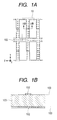
- FIG. 1A is a top view illustrating an etching mask pattern according to a first embodiment of the present invention
- FIG. 1B is a sectional view taken along a line 1B-1B of FIG. 1A .
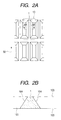
- FIG. 2A is a top view illustrating a structure according to the first embodiment
- FIG. 2B is a sectional view taken along a line 2B-2B of FIG. 2A .
- FIG. 3A is a top view illustrating an etching mask pattern as a formation unit of a structure according to the first embodiment
- FIG. 3B is a top view illustrating the structure according to the first embodiment.
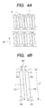
- FIG. 4A is a top view illustrating the structure formed when an alignment error occurs in the first embodiment
- FIG. 4B is an enlarged top view illustrating the structure formed when the alignment error occurs.
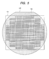
- FIG. 5 is a schematic top view illustrating a silicon wafer according to the present invention.
- FIG. 6A is a top view illustrating details of the etching mask pattern according to the first embodiment
- FIG. 6B is a top view illustrating an etching mask pattern in a related art.
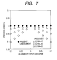
- FIG. 7 is a graph for comparing processing errors due to an alignment error in the present invention and the related art.
- FIG. 8A is a top view illustrating an etching mask pattern according to a modification of the first embodiment
- FIG. 8B is a top view illustrating an etching mask pattern according to another modification of the first embodiment.
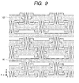
- FIG. 9 is a top view illustrating an etching mask pattern according to a second embodiment of the present invention.
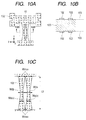
- FIG. 10A is a top view illustrating an etching mask pattern as a formation unit of a micro oscillator according to the second embodiment
- FIG. 10B is a sectional view taken along a line 10B-10B of FIG. 10A
- FIG. 10C is a top view illustrating an etching mask pattern as a formation unit of a structure according to the second embodiment.
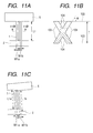
- FIG. 11A is a top view illustrating a micro oscillator manufactured by silicon processing in the second embodiment
- FIG. 11B is a sectional view taken along a line 11B-11B of FIG. 11A
- FIG. 11C is a top view illustrating the micro oscillator manufactured when an alignment error occurs in the second embodiment.
- FIG. 12A is a top view of a light deflector manufactured by silicon processing in the second embodiment
- FIG. 12B is a sectional view illustrating a movable section of the light deflector manufactured by silicon processing in the second embodiment
- FIG. 12C is a schematic perspective view illustrating an optical apparatus including a light deflector manufactured by silicon processing according to a third embodiment of the present invention.
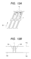
- FIG. 13A is a top view illustrating a structure according to a modification of the first embodiment
- FIG. 13B is a sectional view taken along a line 13B-13B of FIG. 13A .
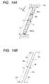
- FIG. 14A is a top view illustrating an etching mask pattern as a formation unit of a structure according to the modification of the first embodiment
- FIG. 14B is a top view illustrating the structure according to the modification of the first embodiment.
- Embodiments of the present invention are described below. What is important in a silicon processing method, a silicon substrate with etching mask, and the like according to the present invention is as described below.
- a determining section for determining width W1 of a structure is formed in an etching mask pattern to prevent the width of the etching mask pattern other than the determining section from being set smaller than the width of the determining section (to set the width of the etching mask pattern other than the determining section larger than the width of the determining section).
- basic embodiments of the silicon processing method, the silicon substrate with etching mask, and the like according to the present invention have configurations described below.
- a mask pattern is formed on a single-crystal silicon substrate, a principal plane of which is a (100) surface and a crystal surface equivalent thereto or a (110) surface and a crystal surface equivalent thereto.
- Crystal anisotropic etching is applied to the single-crystal silicon substrate to form a structure including a (111) surface and a crystal surface equivalent thereto or the like and having width W1 and length L1.
- the mask pattern has a determining section having the width W2 for determining the width W1 of the structure.
- the width of the mask pattern other than the determining section is larger than the width W2 over a length direction of the mask pattern.
- the determining section having the width W2 can be caused to present near the center of the length L1.
- the mask pattern can have a recess.
- the determining section having the width W2 can be formed by the recess.
- the width of the mask pattern can be increased over the length L1 direction in proportion to a distance from the determining section having the width W2.
- This form is adopted in an example illustrated in FIG. 8B and a second embodiment.
- a mask pattern corresponding to a target shape of a structure including a (111) surface and a crystal surface equivalent thereto or the like and having width W1 and length L1 is formed on a single-crystal silicon substrate.
- the single-crystal silicon substrate has a (100) surface and a crystal surface equivalent thereto or a (110) surface and a crystal surface equivalent thereto as a principal plane.
- the mask pattern has a determining section having width W2 for determining the width W1 of the structure.
- the width of the mask pattern other than the determining section is larger than the width W2 over a length direction of the mask pattern.
- the structure can be formed to be a torsion spring as described in detail in first and second embodiments later. It is possible to configure a micro oscillator including, together with the torsion spring, a supporting substrate and a movable section supported by the torsion spring to be capable of torsionally oscillating around a torsion axis with respect to the supporting substrate.
- the micro oscillator has at least one resonant frequency around the torsion axis.
- the structure is formed to be the torsion spring by the silicon processing method.
- an optical apparatus such as an image forming apparatus described in detail in a third embodiment later including a light deflector consisting of a micro oscillator manufactured by the method of manufacturing a micro oscillator a movable section of which oscillator is applied to the reflecting mirror.
- the light deflector reflects and deflects a light beam from a light source and makes at least a part of the light beam incident on a light irradiation target such as a photosensitive member.
- the width of the mask pattern other than the determining section is not smaller than the width of the determining section of the mask pattern for determining the width W1 of the structure, even if there in an alignment error between a crystal axis direction and an etching mask, a structure with less processing dimension error can be formed.
- a silicon processing method and a configuration example of a structure processed by the silicon processing method are described as a first embodiment of the present invention.
- FIG. 5 is a top view of a silicon wafer 100 used for the silicon processing method according to this embodiment.
- the silicon wafer 100 is a single crystal of silicon.
- a normal direction on a paper surface of FIG. 5 is a ⁇ 100> crystal axis direction.
- the silicon wafer 100 has an orientation flat 105 indicating a ⁇ 110> crystal axis direction.
- An etching mask pattern 101 is formed on the surface of the silicon wafer 100. Plural structures can be formed by one wafer. Even if the etching mask pattern 101 has an alignment error with respect to the ⁇ 110> crystal axis direction, a processing dimension error of a structure to be formed can be reduced by the silicon processing method according to this embodiment.
- FIGS. 1A and 1B to FIGS. 3A and 3B are enlarged diagrams of a part of the etching mask pattern 101 or a structure illustrated in FIG. 5 . A relation between an etching mask and a processed structure is described with reference to these figures.
- FIG. 1A is an enlarged top view of a part of the etching mask pattern 101.
- FIG. 1B is a sectional view taken along a line 1B-1B of FIG. 1A .
- the etching mask pattern 101 of silicon nitride is formed by photolithography.
- the etching mask pattern 101 according to this embodiment has a pattern of a silicon nitride film 102 illustrated in the figure in which a plurality of formation units 10 of a structure indicated by a broken line is arrayed.
- a coordinate of the etching mask pattern 101 is set in a direction illustrated in FIG. 1A .
- the etching mask pattern 101 is formed with the x direction aligned in the ⁇ 110> crystal axis direction indicated by the orientation flat 105 illustrated in FIG. 5 .
- a surface on which a pattern is formed in FIG. 1A is a (100) surface of the silicon wafer 100 and a crystal surface 103 equivalent thereto.
- a silicon nitride film 102 is uniformly formed on the rear surface.
- FIGS. 2A and 2B illustrate a state in which, after steps of FIGS. 1A and 1B , anisotropic etching is applied to the silicon wafer 100 with an alkali solution to remove the silicon nitride films on both sides of the silicon wafer 100.
- an alkali solution potassium hydroxide solution and the like can be used.
- FIG. 2A is a top view of a section same as that illustrated in FIG. 1A .
- FIG. 2B is a sectional view taken along a line 2B-2B of FIG. 2A .
- a single-crystal silicon structure 1 fixed at both ends is formed in the section of the formation unit 10 of the structure.
- the structure 1 has a trapezoidal section surrounded by a (111) surface and a crystal surface 104 equivalent thereto and the (100) surface and the crystal surface 103 equivalent thereto.
- an arrow 50 indicates the ⁇ 110> crystal axis direction.
- FIGS. 3A and 3B A correspondence relation between dimensions of the etching mask pattern 101 and the structure 1 described with reference to FIGS. 1A and 2A is described with reference to FIGS. 3A and 3B .
- Enlarged diagrams of the formation unit 10 of a structure illustrated in FIGS. 1A and 2A are respectively illustrated as FIGS. 3A and 3B .
- the etching mask pattern 101 has length L2 corresponding to the length L1 of the structure.
- an x direction of the coordinate is set in the length L2 direction.
- the etching mask pattern 101 has width W(x) in a coordinate y direction. In the present invention, the width W(x) is distributed over the coordinate x direction.
- the width W(x) is not fixed (for example, continuously changes as illustrated in FIG. 8B ) and the etching mask pattern 101 has the minimum width W2 in a range of the length L2.
- a recess 11 is formed in a section in the center of L2 to form the minimum width W2.
- the width W(x) of a section where the recess 11 is not formed is uniformly Wmax.
- the structure 1 is formed as illustrated in FIG. 3B .
- the formed structure 1 has the length L1 as illustrated in the figure.
- the structure 1 has the width W1 in a direction perpendicular to the length L1.
- W1 is determined by the (111) surface and the crystal surface 104 equivalent thereto and is substantially a fixed value over the length L1.
- FIG. 3B illustrates a state in which the coordinate x direction in FIG. 3A is ideally aligned with the ⁇ 110> crystal axis direction indicated by the orientation flat 105 of the silicon wafer 100.
- a second term of the right side of Expression 1 is an amount generally taken into account as an etching mask for performing anisotropic etching and is evident as a relation between a structure to be formed and the etching mask. Therefore, in the following description, this term is omitted.
- an etching amount of the (111) surface and the crystal surface 104 equivalent thereto is taken into account for an etching mask for forming dimensions determined by the (111) surface and the crystal surface 104 equivalent thereto and this term is omitted in the described relation.
- the width W2 of the etching mask pattern 101 is a section for determining W1 of the structure 1 to be formed. This is because silicon is etched on a surface other than the (111) surface and the crystal surface equivalent thereto by anisotropic etching until the width of silicon is reduced to the width W2. At the width W2, the (111) surface and the crystal surface equivalent thereto appear as illustrated in FIG. 3B .
- the width W1 of the structure 1 to be formed has a fixed value in the length L1 direction. Consequently, the width W1 is determined by the width W2, which is the minimum of W(x).
- a processing error of the width W1 due to an alignment error between the ⁇ 110> crystal axis direction and the coordinate x direction of the etching mask pattern 101 is described with reference to FIGS. 4A and 4B , FIGS. 6A and 6B and FIG. 7 .
- Major factors of such an alignment error include an error between the orientation flat 105 and the ⁇ 110> crystal axis direction and an error between the orientation flat 105 and the etching mask pattern 101. These errors typically appear as an angular error of about ⁇ 0.1°. However, in the figures, the angular error is emphasized to facilitate understanding.
- FIG. 4A is a top view of a section equivalent to the section illustrated in FIG. 2A at the time when an alignment error occurs between the coordinate x direction illustrated in FIG. 1A and the ⁇ 110> crystal axis direction 50.
- the structure 1 in FIG. 4A compared with FIG. 2A , the structure 1 is formed to be tilted by the alignment error.
- FIG. 4B is a further enlarged diagram of the formation unit 10 of a structure illustrated in FIG. 4A .
- the structure 1 surrounded by the (111) surface and the crystal surface 104 equivalent thereto has width W1' and length L1'.
- a direction of the length L1' is a direction along the structure 1 determined by the (111) surface and the crystal surface 104 equivalent thereto, i.e., along the ⁇ 110> crystal axis direction.
- a direction of the width W1' is a direction perpendicular to the length L1'. As it is understood from the figures, even when the alignment error occurs, the width of the structure 1 is determined by the (111) surface and the crystal surface 104 equivalent thereto and has a substantially fixed value W1' over the length L1' direction.
- FIGS. 6A and 6B are top views of the etching mask pattern 101 as the formation unit 10 of a structure.
- FIG. 6A illustrates an etching mask pattern according to this embodiment illustrated in FIG. 1A .
- FIG. 6B illustrates an etching mask pattern according to a related art.
- the etching mask pattern according to the related art has a shape illustrated in the figure having length L2 and width W4.
- the width W4 is fixed in the length L2 direction.
- FIGS. 6A and 6B illustrate, as explanation of occurrence of an alignment error, a processed surface 106 as a contour line of the structure 1 after anisotropic etching.
- the processed surface 106 is a line formed when the (111) surface and the crystal surface equivalent thereto, which remain after etching by an etching mask and the surface of a wafer, cross each other.
- the width W1' of the structure 1 to be formed is determined by a space in the ⁇ 110> crystal axis direction between two corners 12. This is because the (111) surface and the crystal surface equivalent thereto first appear in the places of the two corners 12 and, thereafter, etching on both sides of the silicon nitride film 102 having the width W4 and the length L2 stops respectively in a place where the (111) surface and the crystal surface equivalent thereto appears. The place is connected to the (111) surface and the crystal surface equivalent thereto. Therefore, compared with the width W4 of the structure 1 in the ideal state without an alignment error, the width W1' is small.
- the processing error ⁇ due to an alignment error is large. Therefore, in general, when a structure with a large value of L2/W4, for example, a beam, a spring, or an arrayed partition wall is formed by anisotropic etching, the processing error ⁇ is a main cause of a processing error in width.
- the etching mask pattern has the width W2 in the center of the length L2.
- the width W2 is set to a value equal to the width W4 of the structure 1 desired to be formed.
- Wmax is determined by an assumed alignment error ⁇ .
- Wmax is set according to a relation of the following expression: Wmax ⁇ W ⁇ 2 + 2 ⁇ L ⁇ 2 / 2 ⁇ tan ⁇ *
- the two corners 12 does not determine the width W1 of the structure to be formed.
- the processing error ⁇ with respect to the alignment error ⁇ can be reduced to an extremely small value.
- the processing error ⁇ does not depend on the length L2 of the structure. Therefore, even a structure shape, in which a processing error is large according to the related art, can be formed at high accuracy.
- a graph of FIG. 7 indicates relations between the alignment error ⁇ and the processing error ⁇ caused when the etching mask patterns according to the related art and this embodiment are used.
- the processing error ⁇ of this embodiment is about -6 ppm
- the processing error ⁇ is about -10%. In this way, in this embodiment, for a structure having any value of L2/W4, it is possible to reduce a processing error in width of the structure due to an alignment error.
- the silicon processing method by the etching mask according to this embodiment even if there is an alignment error between an actual crystal axis direction and the etching mask, a processing error of a structure due to anisotropic etching can be reduced. Since a smooth plane is obtained by silicon processing by the anisotropic etching, even a structure having small width and large length used as an elastic member can be formed in a form with high processing accuracy and less easily broken.
- a processing error in width of the structure caused by that portion can also be reduced.
- a section having the width W2 is formed by using a recess and an area of other sections having large width is increased, a probability of occurrence of a processing error in width of the structure due to these defects can be further reduced.
- a main shape of an etching mask pattern can be formed by a combination of rectangles. Therefore, when an etching mask pattern is formed by photolithography, the structure of a photomask can be simplified. Therefore, the etching mask pattern can be inexpensively formed.
- the etching mask according to the present invention can reduce a processing error even when the section having the width W2 is not located in the center of the length L2 unlike this embodiment.
- FIG. 8A illustrates a modification of the etching mask in which the section having the width W2 illustrated in FIG. 6A is not located in the center of the length L2.
- values of widths W5 and W6 other than the width W2 have the following relation: W ⁇ 5 ⁇ W ⁇ 2 + 2 ⁇ L ⁇ 6 ⁇ tan ⁇ * W ⁇ 6 ⁇ W ⁇ 2 + 2 ⁇ L ⁇ 7 ⁇ tan ⁇ *
- a processing error can be reduced as indicated by the graph of FIG. 7 .
- a maximum of the width W(x) of the etching mask can be reduced to a smallest value. Therefore, a difference between the maximum width of the etching mask and the width of a final shape formed by anisotropic etching can be reduced. Consequently, it is possible to reduce an etching amount until the (111) surface and the crystal surface equivalent thereto are exposed during etching and form a smooth etching surface. If the difference between the maximum width of the etching mask and the width of the final shape increases, an etching speed error is likely to be caused by update of liquid during etching, accumulation of generated air bubbles, and the like. However, it is possible to reduce the etching speed error. Further, the etching mask in a section where silicon is etched tends to be broken before removal. However, since an area of such a section can be reduced, a processing method with high reliability can be obtained.
- FIG. 8B illustrates another modification of the etching mask as the formation unit 10 of a structure. Components having functions same as those illustrated in FIG. 6A are denoted by the same reference numerals and signs.
- the section having the width W2 is located in the center of the length L2 as in FIG. 6A .
- the width W(x) monotonously increases to the section having the width Wmax over the length L2.
- FIGS. 11A to 11C a configuration example of a micro oscillator manufactured by the silicon processing method according to this embodiment is illustrated.
- FIG. 11A is a top view of the micro oscillator and
- FIG. 11B is a sectional view taken along line 11B-11B of FIG. 11A .
- FIGS. 12A to 12C are diagrams illustrating a light deflector including the micro oscillator according to this embodiment.
- FIG. 12A is a top view of the light deflector and FIG. 12B is a sectional view taken along a line 12B-12B of FIG. 12A .
- components having functions same as those in the first embodiment are denoted by the same reference numerals and signs.
- reference numeral 2 denotes a supporting section
- 3 denotes a fixing section
- 4 denotes a reflection surface
- 6 denotes a movable section
- 7 denotes a permanent magnet forming a driving unit
- 8 denotes a torsion axis.
- the micro oscillator illustrated in FIGS. 11A to 11C is formed as a light deflector that scans light.
- the micro oscillator when the micro oscillator is fixed to the fixing section 3, which is mechanically grounded, via the supporting section 2, the micro oscillator is a torsion oscillator including the structure 1 having the torsion axis 8 set as a torsion center.
- torque is generated by applying an AC magnetic flux 15 from a magnetic field generating unit (also forming the driving unit) not illustrated in the figure such as a coil and causing the AC magnetic flux 15 to act on the permanent magnet 7.
- the micro oscillator can be oscillated around the torsion axis 8 near a resonant frequency.
- the structure 1 of the micro oscillator according to this embodiment is formed by anisotropic etching of silicon by an alkali solution as in the first embodiment. Therefore, surfaces forming the structure 1 are, as illustrated in the figure, the (100) surface and the crystal surface equivalent thereto or the (111) surface and the crystal surface equivalent thereto. As illustrated in the figure, in the structure 1 according to this embodiment, two thin square sections are combined to form an X-shaped polygon.
- L1 2800 ⁇ m
- T 300 ⁇ m.
- f is about 2.7 kHz.
- the torsion spring constant K is proportional to a cube of the width W1a of the structure 1, a dimension error of W1a has a larger influence on a torsion spring constant error than the length L and the wafer thickness T.
- length L2/width W1a 33.
- the width of the structure 1 of such a shape has a large processing error due to an alignment error in the silicon processing method of the related art.
- a processing error of the width W1a of the structure 1 can be reduced.
- a spring constant error can be effectively reduced.
- FIG. 9 is an enlarged top view of the etching mask pattern 101 formed on the silicon wafer 100 illustrated in FIG. 5 .
- the etching mask pattern 101 is formed with the coordinate x direction in FIG. 9 aligned with the ⁇ 110> crystal axis direction indicated by the orientation flat 105 illustrated in FIG. 5 .
- a broken line section illustrated in FIG. 9 indicates a formation unit 16 of a micro oscillator.
- plural micro oscillators can be formed adjacent to one another.
- a structure formation planned section and an oscillator formation planned section of the silicon nitride film 102 are arranged close to each other in adjacent elements.
- FIG. 10A An enlarged top view of the formation unit 16 of a micro oscillator is illustrated in FIG. 10A .
- a sectional view along a line 10B-10B of FIG. 10A is illustrated in FIG. 10B .
- FIG. 10C An enlarged top view of the formation unit 10 of a structure is illustrated in FIG. 10C .
- the formation unit 10 of a structure according to this embodiment has a characteristic pattern in order to form the structure 1 having the X-shaped section illustrated in FIGS. 11A to 11C .
- the formation unit 10 generally has a shape formed by arranging a pair of the patterns illustrated in FIG. 8B .
- the pattern illustrated in FIG. 10A is also formed on a rear surface. Therefore, anisotropic etching by an alkali solution is also performed from both the front and rear surfaces of the wafer.
- the widths Wa(x) and Wb(x) of the etching mask pattern have distributions in the x direction.
- the etching mask pattern has widths W2a and W2b in the center of the length L2. Further away from the center, the widths Wa(x) and Wb(x) monotonously increase to reach a maximum Wmax.
- Wmax is set to have the following relation with respect to the assumed alignment error range ⁇ * under the same principle as Equation 7 described above: Wmax ⁇ W ⁇ 2 ⁇ a + 2 ⁇ L ⁇ 2 / 2 ⁇ tan ⁇ *
- the micro oscillator illustrated in FIGS. 11A to 11C is formed.
- the micro oscillator formed when the alignment error ⁇ occurs is described.
- the micro oscillator has a shape illustrated in the top view of FIG. 11C .
- a principle of occurrence of a processing error due to the alignment error ⁇ is the same as that in the first embodiment.
- the micro oscillator according to this embodiment has the X shape in section as illustrated in FIG. 11B , the width and the length of the structure 1 appear as lengths L1a and L2b and widths W1a' and W1b' illustrated in FIG. 11C .
- the length of the structure 1 an average of L1a and L2b only has to be set as representative length.
- the processing error ⁇ of width is set as (W1a'-W2a)/W2a.
- the single-crystal silicon substrate the principal plane of which is the (100) surface and the crystal surface equivalent thereto.
- the same processing can be performed by a single-crystal silicon substrate, a principal plane of which is the (110) surface and the crystal surface equivalent thereto.
- a mask pattern is formed on the principal plane of the single-crystal silicon substrate, the principal plane of which is the (110) surface and the crystal surface equivalent thereto, and subjected to crystal anisotropic etching. Consequently, as illustrated in FIGS. 13A and 13B corresponding to FIGS.
- the structure 1 having width and length including the (110) surface and the crystal surface 110 equivalent thereto and the (111) surface and the crystal surface 104 equivalent thereto perpendicular to the (110) surface and the crystal surface 110 equivalent thereto.
- an arrow 51 indicates a ⁇ 111> crystal axis direction.
- the width of a determining section for the width W1 of the structure is the width W2.
- the width of the mask pattern other than the determining section is larger than the width W2 over the length direction of the mask pattern.
- a section of the structure 1 of a form corresponding to the first embodiment is formed in a rectangular shape.
- a section of the structure 1 of a form corresponding to the second embodiment is formed in a shape in which two thin square sections are arranged in parallel.
- FIG. 12C is a schematic perspective view illustrating an optical apparatus according to the third embodiment in which the light deflector illustrated in FIGS. 12A to 12C in the second embodiment is used.
- reference numeral 3003 denotes the light deflector according to the second embodiment, which one-dimensionally scans incident light.
- Reference numeral 3001 denotes a laser beam source as a light source.
- Reference numeral 3002 denotes a lens or a lens group, 3004 denotes a writing lens or a writing lens group, and 3005 denotes a drum-like photosensitive member as a light irradiation target.
- a laser beam emitted from the laser beam source 3001 is subjected to predetermined intensity modulation related to timing for light deflection scanning.
- This intensity modulated light is one-dimensionally scanned by the optical scanning system (the light deflector) 3003 through the lens or the lens group 3002.
- the scanned laser beam forms an image on the photosensitive member 3005 through the writing lens or the writing lens group 3004.
- the photosensitive member 3005 rotated around a rotation axis in a direction perpendicular to a scanning direction is uniformly charged by a charger not illustrated in the figure.
- a charger not illustrated in the figure.
- an electrostatic latent image is formed on a scanned section of the photosensitive member 3005.
- a toner image is formed in an image section of the electrostatic latent image by a developing device not illustrated in the figure.
- An image is formed on a sheet by, for example, transferring the toner image onto a sheet not illustrated in the figure and fixing the toner image.
- a stable image can be formed at lower power consumption by the light deflector 3003 according to the second embodiment with less error of a resonant frequency.
- the light deflector can be used in other optical apparatuses.
- the light deflector reflects and deflects a light beam from a light source and makes at least a part of the light beam incident on a light irradiation target.
- optical apparatuses include, besides image forming apparatuses such as a laser beam printer, an image display apparatus and an apparatus that scans a light beam such as a barcode reader.
- the silicon processing method according to the present invention can be applied to manufacturing of micro structures of, besides the optical apparatuses, for example, an acceleration sensor and an angular velocity sensor manufactured by using the micro machine technique.
- a silicon processing method includes: forming a mask pattern on a principal plane of a single-crystal silicon substrate; and applying crystal anisotropic etching to the principal surface to form a structure including a (111) surface and a crystal surface equivalent thereto and having width W1 and length L1.
- the principal plane includes a (100) surface and a crystal surface equivalent thereto or a (110) surface and a crystal surface equivalent thereto.
- a determining section for determining the width W1 of the structure is formed in the mask pattern.
- the width of the determining section for the width W1 of the mask pattern is width W2.
- the width of the mask pattern other than the determining section is larger than the width W2 over a length direction of the mask pattern.
Landscapes
- Engineering & Computer Science (AREA)
- Manufacturing & Machinery (AREA)
- Microelectronics & Electronic Packaging (AREA)
- Physics & Mathematics (AREA)
- Geometry (AREA)
- Micromachines (AREA)
- Mechanical Optical Scanning Systems (AREA)
- Mechanical Light Control Or Optical Switches (AREA)
- Weting (AREA)
Abstract
A silicon processing method includes: forming a mask pattern on a principal plane of a single-crystal silicon substrate; and applying crystal anisotropic etching to the principal surface to form a structure including a (111) surface and a crystal surface equivalent thereto and having width W1 and length L1. The principal plane includes a (100) surface and a crystal surface equivalent thereto or a (110) surface and a crystal surface equivalent thereto. A determining section for determining the width W1 of the structure is formed in the mask pattern. The width of the determining section for the width W1 of the mask pattern is width W2. The width of the mask pattern other than the determining section is larger than the width W2 over a length direction of the mask pattern.
Description
- The present invention relates to a method of manufacturing a micro machine member and the like from a silicon wafer according to a semiconductor process, and, more particularly to a silicon processing method for manufacturing a silicon structure from a wafer, a silicon substrate with etching mask, and the like. The structure is used as, for example, an elastic member and configures a micro oscillator that performs oscillation. The oscillator can be used for optical apparatuses such as a light deflector and an image forming apparatus using the light deflector, sensors such as an acceleration sensor and an angular velocity sensor, and the like.
- Conventionally, micro machine members manufactured from a wafer according to a semiconductor process can be processed in a micrometer order. Various micro functional elements are realized by using the micro machine members (see, Japanese Patent Application Laid-Open No.
H06-232112 - In a silicon micro functional element, a structure subjected to stress is often used. With the anisotropic etching, a member having a smooth processed surface can be obtained. In particular, when the structure subjected to stress is formed, since the smooth surface can avoid stress concentration, a structure having satisfactory durability can be manufactured.
- A light deflector that performs optical scanning by torsionally oscillating a reflection surface with a micro oscillator formed by such a technique (see United States Patent No.
4,317,611 ) has, for example, the following characteristics compared with an optical scanning optical system that uses a rotary multisurface mirror such as a polygon mirror: the light deflector can be reduced in size and power consumption is small. In particular, power consumption can be further reduced by driving the light deflector near a resonant frequency of the torsional oscillation of the micro oscillator. - However, as one of problems of the method of manufacturing a structure from a wafer according to the anisotropic etching, an error occurs in a processing dimension between a formed etching mask and a crystal axis direction of the wafer because of an alignment error. For example, when such a structure is used as a spring to manufacture a micro oscillator, a spring constant error occurs because of the processing dimension error. This is likely to lead to a manufacturing error of a resonant frequency of the micro oscillator.
- In view of the problems, a silicon processing method according to the present invention has characteristics described below. The silicon processing method is a silicon processing method including forming a mask pattern on a principal plane of a single-crystal silicon substrate and applying crystal anisotropic etching to the principal surface to form a structure including a (111) surface and a crystal surface equivalent thereto and having width W1 and length L1. The principal plane is formed by one of a (100) surface and a crystal surface equivalent thereto (these are collectively referred to as (100) equivalent surface as well) and a (110) surface and a crystal surface equivalent thereto (these are collectively referred to as (110) equivalent surface as well). A determining section for determining the width W1 of the structure is formed in the mask pattern. The width of the determining section for the width W1 of the mask pattern is width W2. The width of the mask pattern other than the determining section is larger than the width W2 over a length direction of the mask pattern.
- The determining section having the width W2 can be caused to be present near the center of the length L1. The mask pattern can have a recess, and the determining section having the width W2 can be formed by the recess.
- The width of the mask pattern can be increased over the length L1 direction in proportion to a distance from the determining section having the width W2.
- In the silicon processing method, when an angle formed by the width W2 direction and the width W1 direction is represented as an angle θ, the width W2 can have a relation W1 = W2·cosθ.
- In the silicon processing method, when a distance from the determining section having the width W2 of the mask pattern is represented as x, a distribution of widths of the mask pattern over the length direction of the mask pattern is represented as W(x), and a maximum tolerance of the angle formed by the width W2 direction and the width W1 direction is represented as θ*, a relation W(x) ≥ W2 + 2·|x|·tanθ* can be satisfied.
- In view of the problems, a silicon substrate with etching mask according to the present invention has characteristics described below. A mask pattern corresponding to a target shape of a structure including a (111) surface and a crystal surface equivalent thereto and having width W1 and length L1 is formed on a single-crystal silicon substrate. The single-crystal silicon substrate has one of a (100) surface and a crystal surface equivalent thereto and a (110) surface and a crystal surface equivalent thereto as a principal plane. The mask pattern has a determining section for determining the width W1 of the structure. The width of the determining section for the width W1 of the mask pattern is the width W2. The width of the mask pattern other than the determining section is larger than the width W2 over a length direction of the mask pattern.
- In view of the problems, a method of manufacturing a micro oscillator according to the present invention has characteristics described below. The method is a method of manufacturing a micro oscillator including a supporting substrate, a torsion spring, and a movable section supported by the torsion spring to be capable of torsionally oscillating around a torsion axis with respect to the supporting substrate. The micro oscillator has at least one resonant frequency around the torsion axis. The structure is formed to be the torsion spring by the silicon processing method.
- In view of the problems, an optical apparatus such as an image forming apparatus according to the present invention includes a light deflector having a micro oscillator manufactured by the method of manufacturing a micro oscillator and a light deflecting element provided in the movable section. The light deflector reflects and deflects a light beam from a light source and makes at least a part of the light beam incident on a light irradiation target such as a photosensitive member.
- According to the present invention, the width of the mask pattern other than the determining section is set larger than the width of the determining section of the mask pattern for determining the width W1 of the structure. Therefore, even if there is an alignment error between a crystal axis direction and the etching mask, it is possible to realize silicon processing that can form a structure with less processing dimension error. Therefore, for example, if the structure formed by the silicon processing method according to the present invention is used as a spring of the micro oscillator, it is possible to reduce a spring constant error due to manufacturing.
- Further features of the present invention will become apparent from the following description of exemplary embodiments with reference to the attached drawings.
-
FIG. 1A is a top view illustrating an etching mask pattern according to a first embodiment of the present invention, andFIG. 1B is a sectional view taken along aline 1B-1B ofFIG. 1A . -
FIG. 2A is a top view illustrating a structure according to the first embodiment, andFIG. 2B is a sectional view taken along aline 2B-2B ofFIG. 2A . -
FIG. 3A is a top view illustrating an etching mask pattern as a formation unit of a structure according to the first embodiment, andFIG. 3B is a top view illustrating the structure according to the first embodiment. -
FIG. 4A is a top view illustrating the structure formed when an alignment error occurs in the first embodiment, andFIG. 4B is an enlarged top view illustrating the structure formed when the alignment error occurs. -
FIG. 5 is a schematic top view illustrating a silicon wafer according to the present invention. -
FIG. 6A is a top view illustrating details of the etching mask pattern according to the first embodiment, andFIG. 6B is a top view illustrating an etching mask pattern in a related art. -
FIG. 7 is a graph for comparing processing errors due to an alignment error in the present invention and the related art. -
FIG. 8A is a top view illustrating an etching mask pattern according to a modification of the first embodiment, andFIG. 8B is a top view illustrating an etching mask pattern according to another modification of the first embodiment. -
FIG. 9 is a top view illustrating an etching mask pattern according to a second embodiment of the present invention. -
FIG. 10A is a top view illustrating an etching mask pattern as a formation unit of a micro oscillator according to the second embodiment;FIG. 10B is a sectional view taken along aline 10B-10B ofFIG. 10A; and FIG. 10C is a top view illustrating an etching mask pattern as a formation unit of a structure according to the second embodiment. -
FIG. 11A is a top view illustrating a micro oscillator manufactured by silicon processing in the second embodiment;FIG. 11B is a sectional view taken along aline 11B-11B ofFIG. 11A; and FIG. 11C is a top view illustrating the micro oscillator manufactured when an alignment error occurs in the second embodiment. -
FIG. 12A is a top view of a light deflector manufactured by silicon processing in the second embodiment;FIG. 12B is a sectional view illustrating a movable section of the light deflector manufactured by silicon processing in the second embodiment; andFIG. 12C is a schematic perspective view illustrating an optical apparatus including a light deflector manufactured by silicon processing according to a third embodiment of the present invention. -
FIG. 13A is a top view illustrating a structure according to a modification of the first embodiment, andFIG. 13B is a sectional view taken along aline 13B-13B ofFIG. 13A . -
FIG. 14A is a top view illustrating an etching mask pattern as a formation unit of a structure according to the modification of the first embodiment, andFIG. 14B is a top view illustrating the structure according to the modification of the first embodiment. - Embodiments of the present invention are described below. What is important in a silicon processing method, a silicon substrate with etching mask, and the like according to the present invention is as described below. In order to make use of a characteristic of crystal anisotropic etching, a determining section for determining width W1 of a structure is formed in an etching mask pattern to prevent the width of the etching mask pattern other than the determining section from being set smaller than the width of the determining section (to set the width of the etching mask pattern other than the determining section larger than the width of the determining section). Based on this idea, basic embodiments of the silicon processing method, the silicon substrate with etching mask, and the like according to the present invention have configurations described below.
- In a basic embodiment of the silicon processing method, a mask pattern is formed on a single-crystal silicon substrate, a principal plane of which is a (100) surface and a crystal surface equivalent thereto or a (110) surface and a crystal surface equivalent thereto. Crystal anisotropic etching is applied to the single-crystal silicon substrate to form a structure including a (111) surface and a crystal surface equivalent thereto or the like and having width W1 and length L1. The mask pattern has a determining section having the width W2 for determining the width W1 of the structure. The width of the mask pattern other than the determining section is larger than the width W2 over a length direction of the mask pattern.
- In the embodiment, forms described below can be adopted. First, the determining section having the width W2 can be caused to present near the center of the length L1. The mask pattern can have a recess. The determining section having the width W2 can be formed by the recess. These forms are described in a first embodiment later.
- The width of the mask pattern can be increased over the length L1 direction in proportion to a distance from the determining section having the width W2. This form is adopted in an example illustrated in
FIG. 8B and a second embodiment. When an angle formed by the width W2 direction and the width W1 direction (i.e., an alignment error) is represented as an angle θ, the width W2 can be set to have a relation W1 = W2·cosθ. When a distance from the determining section of the mask pattern is represented as x, a distribution of widths of the mask pattern over the length direction of the mask pattern is represented as W(x), and a maximum tolerance of the angle formed by the width W2 direction and the width W1 direction is represented as θ*, a relation W(x) ≥ W2 + 2·|x|·tanθ* is satisfied. These forms are also described in detail in the first embodiment later. - In a basic embodiment of the silicon substrate with etching mask, a mask pattern corresponding to a target shape of a structure including a (111) surface and a crystal surface equivalent thereto or the like and having width W1 and length L1 is formed on a single-crystal silicon substrate. The single-crystal silicon substrate has a (100) surface and a crystal surface equivalent thereto or a (110) surface and a crystal surface equivalent thereto as a principal plane. The mask pattern has a determining section having width W2 for determining the width W1 of the structure. The width of the mask pattern other than the determining section is larger than the width W2 over a length direction of the mask pattern. The specific forms described above can be adopted.
- According to the silicon processing method, the structure can be formed to be a torsion spring as described in detail in first and second embodiments later. It is possible to configure a micro oscillator including, together with the torsion spring, a supporting substrate and a movable section supported by the torsion spring to be capable of torsionally oscillating around a torsion axis with respect to the supporting substrate. The micro oscillator has at least one resonant frequency around the torsion axis. The structure is formed to be the torsion spring by the silicon processing method.
- It is also possible to configure an optical apparatus such as an image forming apparatus described in detail in a third embodiment later including a light deflector consisting of a micro oscillator manufactured by the method of manufacturing a micro oscillator a movable section of which oscillator is applied to the reflecting mirror. The light deflector reflects and deflects a light beam from a light source and makes at least a part of the light beam incident on a light irradiation target such as a photosensitive member.
- In the embodiments, since the width of the mask pattern other than the determining section is not smaller than the width of the determining section of the mask pattern for determining the width W1 of the structure, even if there in an alignment error between a crystal axis direction and an etching mask, a structure with less processing dimension error can be formed.
- Embodiments of the present invention are described below with reference to the accompanying drawings.
- First embodiment
- A silicon processing method and a configuration example of a structure processed by the silicon processing method are described as a first embodiment of the present invention.
- First, the silicon processing method according to this embodiment is described with reference to
FIGS. 1A and 1B toFIG. 5. FIG. 5 is a top view of asilicon wafer 100 used for the silicon processing method according to this embodiment. Thesilicon wafer 100 is a single crystal of silicon. A normal direction on a paper surface ofFIG. 5 is a <100> crystal axis direction. Thesilicon wafer 100 has an orientation flat 105 indicating a <110> crystal axis direction. Anetching mask pattern 101 is formed on the surface of thesilicon wafer 100. Plural structures can be formed by one wafer. Even if theetching mask pattern 101 has an alignment error with respect to the <110> crystal axis direction, a processing dimension error of a structure to be formed can be reduced by the silicon processing method according to this embodiment. -
FIGS. 1A and 1B toFIGS. 3A and 3B are enlarged diagrams of a part of theetching mask pattern 101 or a structure illustrated inFIG. 5 . A relation between an etching mask and a processed structure is described with reference to these figures. -
FIG. 1A is an enlarged top view of a part of theetching mask pattern 101.FIG. 1B is a sectional view taken along aline 1B-1B ofFIG. 1A . After silicon nitride films are formed on both sides of thesilicon wafer 100, theetching mask pattern 101 of silicon nitride is formed by photolithography. As illustrated inFIG. 1A , theetching mask pattern 101 according to this embodiment has a pattern of asilicon nitride film 102 illustrated in the figure in which a plurality offormation units 10 of a structure indicated by a broken line is arrayed. With a longitudinal direction of thesilicon nitride film 102 represented by theformation unit 10 of a structure set as an x direction, a coordinate of theetching mask pattern 101 is set in a direction illustrated inFIG. 1A . Theetching mask pattern 101 is formed with the x direction aligned in the <110> crystal axis direction indicated by the orientation flat 105 illustrated inFIG. 5 . As illustrated inFIG. 1B , a surface on which a pattern is formed inFIG. 1A is a (100) surface of thesilicon wafer 100 and acrystal surface 103 equivalent thereto. On the other hand, asilicon nitride film 102 is uniformly formed on the rear surface. -
FIGS. 2A and 2B illustrate a state in which, after steps ofFIGS. 1A and 1B , anisotropic etching is applied to thesilicon wafer 100 with an alkali solution to remove the silicon nitride films on both sides of thesilicon wafer 100. As the alkali solution, potassium hydroxide solution and the like can be used.FIG. 2A is a top view of a section same as that illustrated inFIG. 1A .FIG. 2B is a sectional view taken along aline 2B-2B ofFIG. 2A . As illustrated inFIG. 2A , a single-crystal silicon structure 1 fixed at both ends is formed in the section of theformation unit 10 of the structure. According to the anisotropic etching by the alkali solution, as illustrated inFIG. 2B , thestructure 1 has a trapezoidal section surrounded by a (111) surface and acrystal surface 104 equivalent thereto and the (100) surface and thecrystal surface 103 equivalent thereto. InFIG. 2A , anarrow 50 indicates the <110> crystal axis direction. - A correspondence relation between dimensions of the
etching mask pattern 101 and thestructure 1 described with reference toFIGS. 1A and2A is described with reference toFIGS. 3A and 3B . Enlarged diagrams of theformation unit 10 of a structure illustrated inFIGS. 1A and2A are respectively illustrated asFIGS. 3A and 3B . As illustrated inFIG. 3A , theetching mask pattern 101 has length L2 corresponding to the length L1 of the structure. In a coordinate of theetching mask pattern 101, an x direction of the coordinate is set in the length L2 direction. Theetching mask pattern 101 has width W(x) in a coordinate y direction. In the present invention, the width W(x) is distributed over the coordinate x direction. In other words, the width W(x) is not fixed (for example, continuously changes as illustrated inFIG. 8B ) and theetching mask pattern 101 has the minimum width W2 in a range of the length L2. In this embodiment, in particular, as illustrated inFIG. 3A , arecess 11 is formed in a section in the center of L2 to form the minimum width W2. On the other hand, the width W(x) of a section where therecess 11 is not formed is uniformly Wmax. - According to the
etching mask pattern 101 illustrated inFIG. 3A , thestructure 1 is formed as illustrated inFIG. 3B . The formedstructure 1 has the length L1 as illustrated in the figure. Thestructure 1 has the width W1 in a direction perpendicular to the length L1. As illustrated inFIG. 2B , W1 is determined by the (111) surface and thecrystal surface 104 equivalent thereto and is substantially a fixed value over the length L1. -
FIG. 3B illustrates a state in which the coordinate x direction inFIG. 3A is ideally aligned with the <110> crystal axis direction indicated by the orientation flat 105 of thesilicon wafer 100. The width W1 and the width W2 have the following relation:
- A second term of the right side of
Expression 1 is an amount generally taken into account as an etching mask for performing anisotropic etching and is evident as a relation between a structure to be formed and the etching mask. Therefore, in the following description, this term is omitted. For example,Expression 1 is represented as follows:
- Concerning all other dimensions, unless specifically noted otherwise, an etching amount of the (111) surface and the
crystal surface 104 equivalent thereto is taken into account for an etching mask for forming dimensions determined by the (111) surface and thecrystal surface 104 equivalent thereto and this term is omitted in the described relation. - In the state in which the coordinate x direction is ideally aligned with the <110> crystal axis direction, the width W2 of the
etching mask pattern 101 is a section for determining W1 of thestructure 1 to be formed. This is because silicon is etched on a surface other than the (111) surface and the crystal surface equivalent thereto by anisotropic etching until the width of silicon is reduced to the width W2. At the width W2, the (111) surface and the crystal surface equivalent thereto appear as illustrated inFIG. 3B . - In this way, even if the width W(x) of the
etching mask pattern 101 has a distribution in the length L2 direction, the width W1 of thestructure 1 to be formed has a fixed value in the length L1 direction. Consequently, the width W1 is determined by the width W2, which is the minimum of W(x). - A processing error of the width W1 due to an alignment error between the <110> crystal axis direction and the coordinate x direction of the
etching mask pattern 101 is described with reference toFIGS. 4A and 4B ,FIGS. 6A and 6B andFIG. 7 . Major factors of such an alignment error include an error between the orientation flat 105 and the <110> crystal axis direction and an error between the orientation flat 105 and theetching mask pattern 101. These errors typically appear as an angular error of about ±0.1°. However, in the figures, the angular error is emphasized to facilitate understanding. -
FIG. 4A is a top view of a section equivalent to the section illustrated inFIG. 2A at the time when an alignment error occurs between the coordinate x direction illustrated inFIG. 1A and the <110>crystal axis direction 50. As indicated by thestructure 1 inFIG. 4A , compared withFIG. 2A , thestructure 1 is formed to be tilted by the alignment error.FIG. 4B is a further enlarged diagram of theformation unit 10 of a structure illustrated inFIG. 4A . As illustrated inFIG. 4B , thestructure 1 surrounded by the (111) surface and thecrystal surface 104 equivalent thereto has width W1' and length L1'. A direction of the length L1' is a direction along thestructure 1 determined by the (111) surface and thecrystal surface 104 equivalent thereto, i.e., along the <110> crystal axis direction. A direction of the width W1' is a direction perpendicular to the length L1'. As it is understood from the figures, even when the alignment error occurs, the width of thestructure 1 is determined by the (111) surface and thecrystal surface 104 equivalent thereto and has a substantially fixed value W1' over the length L1' direction. - A principle of reduction of a processing dimension error by the silicon processing method according to the present invention is described with reference to
FIGS. 6A and 6B andFIG. 7 .FIGS. 6A and 6B are top views of theetching mask pattern 101 as theformation unit 10 of a structure.FIG. 6A illustrates an etching mask pattern according to this embodiment illustrated inFIG. 1A . On the other hand,FIG. 6B illustrates an etching mask pattern according to a related art. The etching mask pattern according to the related art has a shape illustrated in the figure having length L2 and width W4. Like a coordinate of theetching mask pattern 101 according to this embodiment, when a coordinate with the length L2 direction set as the x direction is set, the width W4 is fixed in the length L2 direction. The width W4 and the length L2 are designed as follows such that thestructure 1 illustrated inFIG. 3B is formed in an ideal state without an alignment error:

-
FIGS. 6A and 6B illustrate, as explanation of occurrence of an alignment error, a processedsurface 106 as a contour line of thestructure 1 after anisotropic etching. The processedsurface 106 is a line formed when the (111) surface and the crystal surface equivalent thereto, which remain after etching by an etching mask and the surface of a wafer, cross each other. InFIGS. 6A and 6B , an angle θ formed by the <110> crystal axis direction and the coordinate x direction is illustrated as an amount of the alignment error (θ = 0 is an ideal state). - In a silicon processing method according to the related art illustrated in
FIG. 6B , when an alignment error occurs, the width W1' of thestructure 1 to be formed is determined by a space in the <110> crystal axis direction between twocorners 12. This is because the (111) surface and the crystal surface equivalent thereto first appear in the places of the twocorners 12 and, thereafter, etching on both sides of thesilicon nitride film 102 having the width W4 and the length L2 stops respectively in a place where the (111) surface and the crystal surface equivalent thereto appears. The place is connected to the (111) surface and the crystal surface equivalent thereto. Therefore, compared with the width W4 of thestructure 1 in the ideal state without an alignment error, the width W1' is small. A reduction amount of this width is larger as the length L1 of thestructure 1 desired to be formed is larger. W1' and W4 can be approximated in the following relation in an range of an assumed alignment error:
- When a processing error ε of width is set as (W1'-W4)/W4, in the related art, the processing error ε is represented by the following expression:

In the related art, as indicated byExpression 6, in the case of a shape with a large value of L2/W4, the processing error ε due to an alignment error is large. Therefore, in general, when a structure with a large value of L2/W4, for example, a beam, a spring, or an arrayed partition wall is formed by anisotropic etching, the processing error ε is a main cause of a processing error in width. - On the other hand, in an etching mask pattern according to this embodiment illustrated in
FIG. 6A , as described above, there is a distribution of the width W(x) along the coordinate x direction (i.e., the width W(x) is not fixed). As illustrated in the figure, the etching mask pattern has the width W2 in the center of the length L2. The width W2 is set to a value equal to the width W4 of thestructure 1 desired to be formed. In this embodiment, as described above, the width of the section other than therecess 11 is Wmax. Wmax is determined by an assumed alignment error θ. In the case of this embodiment, if an alignment error range in which a processing error is desired to be reduced is ±θ*, Wmax is set according to a relation of the following expression:
- In the etching mask pattern according to this embodiment, even if there is an alignment error, the two
corners 12 does not determine the width W1 of the structure to be formed. The width W2 determines the width W1. This is because the (111) surface and the crystal surface equivalent thereto first appear in places of both sides of the determining section for the width W2 and, thereafter, etching on both sides of other sections of thesilicon nitride film 102 having the length L2 stops respectively in a place where the (111) surface and the crystal surface equivalent thereto appears. The place is connected to the (111) surface and the crystal surface equivalent thereto. Therefore, the width W1' of a structure formed at this point and the processing error ε of the structure are represented by the following expressions:

- Therefore, in the etching mask pattern according to this embodiment, the processing error ε with respect to the alignment error θ can be reduced to an extremely small value. As it is seen from Expression 9, the processing error ε does not depend on the length L2 of the structure. Therefore, even a structure shape, in which a processing error is large according to the related art, can be formed at high accuracy.
- Further, as illustrated in
FIG. 6A , in the etching mask pattern according to the present invention including this embodiment, even if there is acrack 108, apinhole 107, or the like near an edge of the pattern, this does not affect a processing error in width. In the mask pattern of the related art illustrated inFIG. 6B , such a defect of the mask near the edge directly leads to a processing error in width. - A graph of
FIG. 7 indicates relations between the alignment error θ and the processing error ε caused when the etching mask patterns according to the related art and this embodiment are used. As described above, in a range of the alignment error θ ±0.1° that is likely to typically occur, whereas the processing error ε of this embodiment is about -6 ppm, in the related art, when L2/W4 = 60, the processing error ε is about -10%. In this way, in this embodiment, for a structure having any value of L2/W4, it is possible to reduce a processing error in width of the structure due to an alignment error. - As described above, according to the silicon processing method by the etching mask according to this embodiment, even if there is an alignment error between an actual crystal axis direction and the etching mask, a processing error of a structure due to anisotropic etching can be reduced. Since a smooth plane is obtained by silicon processing by the anisotropic etching, even a structure having small width and large length used as an elastic member can be formed in a form with high processing accuracy and less easily broken.
- Even if there are slight defects (a tear, a hole, etc.) in a contour of the etching mask, a processing error in width of the structure caused by that portion can also be reduced. In particular, as in the etching mask according to this embodiment, if a section having the width W2 is formed by using a recess and an area of other sections having large width is increased, a probability of occurrence of a processing error in width of the structure due to these defects can be further reduced.
- As in the etching mask according to this embodiment, if the section having the width W2 is formed by using the recess, a main shape of an etching mask pattern can be formed by a combination of rectangles. Therefore, when an etching mask pattern is formed by photolithography, the structure of a photomask can be simplified. Therefore, the etching mask pattern can be inexpensively formed.
- It goes without saying that the etching mask according to the present invention can reduce a processing error even when the section having the width W2 is not located in the center of the length L2 unlike this embodiment.
-
FIG. 8A illustrates a modification of the etching mask in which the section having the width W2 illustrated inFIG. 6A is not located in the center of the length L2. In this case, if an alignment error range in which a processing error is desired to be reduced is ±θ*, values of widths W5 and W6 other than the width W2 have the following relation:

In the modification illustrated inFIG. 8A , as in this embodiment, a processing error can be reduced as indicated by the graph ofFIG. 7 . - However, like the etching mask according to this embodiment, by locating the section having the width W2 in the center of the length L2, a maximum of the width W(x) of the etching mask can be reduced to a smallest value. Therefore, a difference between the maximum width of the etching mask and the width of a final shape formed by anisotropic etching can be reduced. Consequently, it is possible to reduce an etching amount until the (111) surface and the crystal surface equivalent thereto are exposed during etching and form a smooth etching surface. If the difference between the maximum width of the etching mask and the width of the final shape increases, an etching speed error is likely to be caused by update of liquid during etching, accumulation of generated air bubbles, and the like. However, it is possible to reduce the etching speed error. Further, the etching mask in a section where silicon is etched tends to be broken before removal. However, since an area of such a section can be reduced, a processing method with high reliability can be obtained.
- Further, by adopting a configuration illustrated in
FIG. 8B , it is possible to further reduce the difference between the maximum width of the etching mask and the width of the final shape formed by anisotropic etching.FIG. 8B illustrates another modification of the etching mask as theformation unit 10 of a structure. Components having functions same as those illustrated inFIG. 6A are denoted by the same reference numerals and signs. In the configuration illustrated inFIG. 8B , the section having the width W2 is located in the center of the length L2 as inFIG. 6A . On the other hand, unlikeFIG. 6A , the width W(x) monotonously increases to the section having the width Wmax over the length L2. By forming the etching mask in this way, it is possible to reduce the difference between the maximum width of the etching mask and the width of the final shape of the structure formed by anisotropic etching. - Furthermore, in the configuration illustrated in
FIG. 8B , it is also possible to set the section having the width W2 of the etching mask at one end of the length L2 and monotonously increase the width W(x) toward the section having the width Wmax. However, in such a form, the difference between the maximum width of the etching mask and the width of the final shape of the structure formed by anisotropic etching is relatively large. - Second Embodiment
- A second embodiment of the present invention is described. In
FIGS. 11A to 11C , a configuration example of a micro oscillator manufactured by the silicon processing method according to this embodiment is illustrated.FIG. 11A is a top view of the micro oscillator andFIG. 11B is a sectional view taken alongline 11B-11B ofFIG. 11A .FIGS. 12A to 12C are diagrams illustrating a light deflector including the micro oscillator according to this embodiment.FIG. 12A is a top view of the light deflector andFIG. 12B is a sectional view taken along aline 12B-12B ofFIG. 12A . In these figures, components having functions same as those in the first embodiment are denoted by the same reference numerals and signs. - In the micro oscillator illustrated in
FIGS. 11A to 11C and the light deflector illustrated inFIGS. 12A to 12C ,reference numeral 2 denotes a supporting section, 3 denotes a fixing section, 4 denotes a reflection surface, 6 denotes a movable section, 7 denotes a permanent magnet forming a driving unit, and 8 denotes a torsion axis. As illustrated inFIGS. 12A to 12C , when thereflection surface 4 is formed in themovable section 6 and thepermanent magnet 7 is set on a rear surface of a surface on which thereflection surface 4 is formed, the micro oscillator illustrated inFIGS. 11A to 11C is formed as a light deflector that scans light. In particular, when the micro oscillator is fixed to thefixing section 3, which is mechanically grounded, via the supportingsection 2, the micro oscillator is a torsion oscillator including thestructure 1 having thetorsion axis 8 set as a torsion center. As illustrated inFIG. 12B , torque is generated by applying an ACmagnetic flux 15 from a magnetic field generating unit (also forming the driving unit) not illustrated in the figure such as a coil and causing the ACmagnetic flux 15 to act on thepermanent magnet 7. The micro oscillator can be oscillated around thetorsion axis 8 near a resonant frequency. - The light deflector according to this embodiment has, with respect to the
torsion axis 8, a resonant frequency f in a relation of the following expression:
where, K represents a torsion spring constant around thetorsion axis 8 of thestructure 1 and I represents moment of inertia around thetorsion axis 8 of themovable section 6. - As illustrated in
FIG. 11B , thestructure 1 of the micro oscillator according to this embodiment is formed by anisotropic etching of silicon by an alkali solution as in the first embodiment. Therefore, surfaces forming thestructure 1 are, as illustrated in the figure, the (100) surface and the crystal surface equivalent thereto or the (111) surface and the crystal surface equivalent thereto. As illustrated in the figure, in thestructure 1 according to this embodiment, two thin square sections are combined to form an X-shaped polygon. - When dimensions W1a (= W1b) and L1, wafer thickness T, and an angle Φ (= 54.7°) formed by the (100) surface and the
crystal surface 103 equivalent thereto and the (111) surface and thecrystal surface 104 equivalent thereto are used, the torsion spring constant K of thestructure 1 having the sections can be approximated by the following expression:
- In this embodiment, W1a = W1b = 85 µm, L1 = 2800 µm and T = 300 µm. In the form illustrated in
FIGS. 12A to 12C , f is about 2.7 kHz. - As indicated by Expression 13, since the torsion spring constant K is proportional to a cube of the width W1a of the
structure 1, a dimension error of W1a has a larger influence on a torsion spring constant error than the length L and the wafer thickness T. In addition, length L2/width W1a = 33. The width of thestructure 1 of such a shape has a large processing error due to an alignment error in the silicon processing method of the related art. On the other hand, with the silicon processing method according to the present invention, a processing error of the width W1a of thestructure 1 can be reduced. Further, when thestructure 1 is used as a spring as in this embodiment, a spring constant error can be effectively reduced. - An etching mask pattern of the silicon processing method according to this embodiment is described with reference to
FIG. 9 andFIGS. 10A to 10C . Components having functions same as those in the first embodiment are denoted by the same reference numerals and signs.FIG. 9 is an enlarged top view of theetching mask pattern 101 formed on thesilicon wafer 100 illustrated inFIG. 5 . As in the first embodiment, theetching mask pattern 101 is formed with the coordinate x direction inFIG. 9 aligned with the <110> crystal axis direction indicated by the orientation flat 105 illustrated inFIG. 5 . - A broken line section illustrated in
FIG. 9 indicates aformation unit 16 of a micro oscillator. As illustrated in the figure, in the silicon processing method according to this embodiment, plural micro oscillators can be formed adjacent to one another. A structure formation planned section and an oscillator formation planned section of thesilicon nitride film 102 are arranged close to each other in adjacent elements. - An enlarged top view of the
formation unit 16 of a micro oscillator is illustrated inFIG. 10A . A sectional view along aline 10B-10B ofFIG. 10A is illustrated inFIG. 10B . An enlarged top view of theformation unit 10 of a structure is illustrated inFIG. 10C . Unlike the first embodiment, theformation unit 10 of a structure according to this embodiment has a characteristic pattern in order to form thestructure 1 having the X-shaped section illustrated inFIGS. 11A to 11C . As illustrated inFIGS. 10A to 10C , theformation unit 10 generally has a shape formed by arranging a pair of the patterns illustrated inFIG. 8B . As illustrated inFIG. 10B , the pattern illustrated inFIG. 10A is also formed on a rear surface. Therefore, anisotropic etching by an alkali solution is also performed from both the front and rear surfaces of the wafer. - On the other hand, as in the first embodiment, when the coordinate x direction is set in the length L2 direction, the widths Wa(x) and Wb(x) of the etching mask pattern have distributions in the x direction. The etching mask pattern has widths W2a and W2b in the center of the length L2. Further away from the center, the widths Wa(x) and Wb(x) monotonously increase to reach a maximum Wmax. In particular, W2a and W2b and W1a and W1b illustrated in
FIG. 11A have the following relation:
- Wmax is set to have the following relation with respect to the assumed alignment error range ±θ* under the same principle as
Equation 7 described above:
- With the etching mask pattern described above, the micro oscillator illustrated in
FIGS. 11A to 11C is formed. - The micro oscillator formed when the alignment error θ occurs is described. In this case, the micro oscillator has a shape illustrated in the top view of
FIG. 11C . A principle of occurrence of a processing error due to the alignment error θ is the same as that in the first embodiment. Since the micro oscillator according to this embodiment has the X shape in section as illustrated inFIG. 11B , the width and the length of thestructure 1 appear as lengths L1a and L2b and widths W1a' and W1b' illustrated inFIG. 11C . As the length of thestructure 1, an average of L1a and L2b only has to be set as representative length. Concerning the width of thestructure 1, the widths W1a' and W1b' are equal and have the following relation with the width W2a (= W2b) :

The processing error ε of width is set as (W1a'-W2a)/W2a. - In this way, in the
structure 1 having the X-shaped section as in this embodiment, it is possible to reduce the processing error ε of width with respect to the alignment error θ in a relation same as that described in the first embodiment. In this embodiment, a relation between wafer thickness and with width and the space of the two etching mask patterns arranged in parallel is appropriately set to realize thestructure 1 having the X-shaped section. - As described above, concerning the micro oscillator that performs torsional oscillation around the torsion axis as in this embodiment, since an error of a term of a cube of the width W1a in Expression 13 is reduced, an error of a spring constant can be effectively reduced. Therefore, further, an error of the resonant frequency f of
Expression 12 can also be reduced. When the light deflector illustrated inFIGS. 12A to 12C is formed, since an error of the resonance frequency f is reduced, a light deflector that can be driven at a desired frequency and saved power can be stably manufactured. - In the first and second embodiments, the single-crystal silicon substrate, the principal plane of which is the (100) surface and the crystal surface equivalent thereto, is described. However, the same processing can be performed by a single-crystal silicon substrate, a principal plane of which is the (110) surface and the crystal surface equivalent thereto. Specifically, a mask pattern is formed on the principal plane of the single-crystal silicon substrate, the principal plane of which is the (110) surface and the crystal surface equivalent thereto, and subjected to crystal anisotropic etching. Consequently, as illustrated in
FIGS. 13A and 13B corresponding toFIGS. 2A and 2B , it is possible to form thestructure 1 having width and length including the (110) surface and thecrystal surface 110 equivalent thereto and the (111) surface and thecrystal surface 104 equivalent thereto perpendicular to the (110) surface and thecrystal surface 110 equivalent thereto. InFIG. 13A , anarrow 51 indicates a <111> crystal axis direction. In this case, as illustrated inFIGS. 14A and 14B corresponding toFIGS. 3A and 3B , in the mask pattern, the width of a determining section for the width W1 of the structure is the width W2. The width of the mask pattern other than the determining section is larger than the width W2 over the length direction of the mask pattern. However, the (111) surface and the crystal surface equivalent thereto are perpendicular to the (110) surface and the crystal surface equivalent thereto. Therefore, a section of thestructure 1 of a form corresponding to the first embodiment is formed in a rectangular shape. A section of thestructure 1 of a form corresponding to the second embodiment is formed in a shape in which two thin square sections are arranged in parallel. - Third Embodiment
- A third embodiment of the present invention is described.
FIG. 12C is a schematic perspective view illustrating an optical apparatus according to the third embodiment in which the light deflector illustrated inFIGS. 12A to 12C in the second embodiment is used. - An image forming apparatus is illustrated as the optical apparatus. In
FIG. 12C ,reference numeral 3003 denotes the light deflector according to the second embodiment, which one-dimensionally scans incident light.Reference numeral 3001 denotes a laser beam source as a light source.Reference numeral 3002 denotes a lens or a lens group, 3004 denotes a writing lens or a writing lens group, and 3005 denotes a drum-like photosensitive member as a light irradiation target. - A laser beam emitted from the
laser beam source 3001 is subjected to predetermined intensity modulation related to timing for light deflection scanning. This intensity modulated light is one-dimensionally scanned by the optical scanning system (the light deflector) 3003 through the lens or thelens group 3002. The scanned laser beam forms an image on thephotosensitive member 3005 through the writing lens or the writinglens group 3004. - The
photosensitive member 3005 rotated around a rotation axis in a direction perpendicular to a scanning direction is uniformly charged by a charger not illustrated in the figure. When light is scanned over thephotosensitive member 3005, an electrostatic latent image is formed on a scanned section of thephotosensitive member 3005. Subsequently, a toner image is formed in an image section of the electrostatic latent image by a developing device not illustrated in the figure. An image is formed on a sheet by, for example, transferring the toner image onto a sheet not illustrated in the figure and fixing the toner image. - In this embodiment, a stable image can be formed at lower power consumption by the
light deflector 3003 according to the second embodiment with less error of a resonant frequency. - It goes without saying that the light deflector can be used in other optical apparatuses. In these apparatuses, the light deflector reflects and deflects a light beam from a light source and makes at least a part of the light beam incident on a light irradiation target. Examples of such optical apparatuses include, besides image forming apparatuses such as a laser beam printer, an image display apparatus and an apparatus that scans a light beam such as a barcode reader. The silicon processing method according to the present invention can be applied to manufacturing of micro structures of, besides the optical apparatuses, for example, an acceleration sensor and an angular velocity sensor manufactured by using the micro machine technique.
- While the present invention has been described with reference to exemplary embodiments, it is to be understood that the invention is not limited to the disclosed exemplary embodiments. The scope of the following claims is to be accorded the broadest interpretation so as to encompass all such modifications and equivalent structures and functions.
A silicon processing method includes: forming a mask pattern on a principal plane of a single-crystal silicon substrate; and applying crystal anisotropic etching to the principal surface to form a structure including a (111) surface and a crystal surface equivalent thereto and having width W1 and length L1. The principal plane includes a (100) surface and a crystal surface equivalent thereto or a (110) surface and a crystal surface equivalent thereto. A determining section for determining the width W1 of the structure is formed in the mask pattern. The width of the determining section for the width W1 of the mask pattern is width W2. The width of the mask pattern other than the determining section is larger than the width W2 over a length direction of the mask pattern.
Claims (9)
- A silicon processing method comprising:forming a mask pattern on a principal plane of a single-crystal silicon substrate, the principal plane including one of a (100) surface and a crystal surface equivalent thereto and a (110) surface and a crystal surface equivalent thereto; andapplying crystal anisotropic etching to the principal surface to form a structure including a (111) surface and a crystal surface equivalent thereto and having a width W1 and a length L1, whereina determining section for determining the width W1 of the structure is formed in the mask pattern,a width of the determining section for the width W1 of the mask pattern is a width W2, anda width of the mask pattern other than the determining section is larger than the width W2 over a length direction of the mask pattern.
- The silicon processing method according to claim 1, wherein the determining section having the width W2 is caused to be present near the center of the length L1.
- The silicon processing method according to claim 1 or 2, wherein
the mask pattern has a recess, and
the determining section having the width W2 is formed by the recess. - The silicon processing method according to any one of claims 1 to 3, wherein the width of the mask pattern is increased over the length L1 direction in proportion to a distance from the determining section having the width W2.
- The silicon processing method according to any one of claims 1 to 4, wherein, when an angle formed by the width W2 direction and the width W1 direction is represented as an angle θ, the width W2 has a relation W1 = W2·cosθ.
- The silicon processing method according to claim 5, wherein, when a distance from the determining section having the width W2 of the mask pattern is represented as x, a distribution of widths of the mask pattern over the length direction of the mask pattern is represented as W(x), and a maximum tolerance of the angle formed by the width W2 direction and the width W1 direction is represented as θ*, a relation W(x) ≥ W2 + 2·|x|·tanθ* is satisfied.
- A method of manufacturing a micro oscillator including a supporting substrate, a torsion spring, and a movable section supported by the torsion spring to be capable of torsionally oscillating around a torsion axis with respect to the supporting substrate, the micro oscillator having at least one resonant frequency around the torsion axis, the manufacturing method comprising forming the structure to be the torsion spring with the silicon processing method according to any one of claims 1 to 6.
- An optical apparatus comprising a light deflector having a micro oscillator manufactured by the method of manufacturing a micro oscillator according to claim 7 and a light deflecting element provided in the movable section, wherein
the light deflector reflects and deflects a light beam from a light source and makes at least a part of the light beam incident on a light irradiation target. - A silicon substrate with etching mask comprising, on a single-crystal silicon substrate, the single-crystal silicon substrate having one of a (100) surface and a crystal surface equivalent thereto and a (110) surface and a crystal surface equivalent thereto as a principal plane, a mask pattern corresponding to a target shape including a (111) surface and a crystal surface equivalent thereto and having a width W1 and a length L1 of a structure to be formed, wherein
the mask pattern has a determining section for determining the width W1 of the structure,
a width of the determining section for the width W1 of the mask pattern is a width W2, and
a width of the mask pattern other than the determining section is larger than the width W2 over a length direction of the mask pattern.
Applications Claiming Priority (1)
| Application Number | Priority Date | Filing Date | Title |
|---|---|---|---|
| JP2008221247A JP2010056379A (en) | 2008-08-29 | 2008-08-29 | Silicon processing method and silicon substrate with etching mask |
Publications (1)
| Publication Number | Publication Date |
|---|---|
| EP2159191A2 true EP2159191A2 (en) | 2010-03-03 |
Family
ID=41510795
Family Applications (1)
| Application Number | Title | Priority Date | Filing Date |
|---|---|---|---|
| EP09168828A Withdrawn EP2159191A2 (en) | 2008-08-29 | 2009-08-27 | Silicon processing method and silicon substrate with etching mask |
Country Status (4)
| Country | Link |
|---|---|
| US (1) | US8324113B2 (en) |
| EP (1) | EP2159191A2 (en) |
| JP (1) | JP2010056379A (en) |
| CN (1) | CN101659390A (en) |
Families Citing this family (4)
| Publication number | Priority date | Publication date | Assignee | Title |
|---|---|---|---|---|
| US8535544B2 (en) * | 2010-07-26 | 2013-09-17 | International Business Machines Corporation | Structure and method to form nanopore |
| JP5708290B2 (en) * | 2011-06-17 | 2015-04-30 | セイコーエプソン株式会社 | Manufacturing method of MEMS device, MEMS device, pressure sensor, and ultrasonic transducer |
| JP5624638B2 (en) * | 2013-02-18 | 2014-11-12 | キヤノン株式会社 | Silicon processing method and silicon substrate with etching mask |
| JP6354704B2 (en) * | 2015-08-25 | 2018-07-11 | 日亜化学工業株式会社 | Optical member manufacturing method, semiconductor laser device manufacturing method, and semiconductor laser device |
Citations (2)
| Publication number | Priority date | Publication date | Assignee | Title |
|---|---|---|---|---|
| US4317611A (en) | 1980-05-19 | 1982-03-02 | International Business Machines Corporation | Optical ray deflection apparatus |
| JPH06232112A (en) | 1993-02-08 | 1994-08-19 | Japan Aviation Electron Ind Ltd | Fine processing of silicon wafer |
Family Cites Families (8)
| Publication number | Priority date | Publication date | Assignee | Title |
|---|---|---|---|---|
| JP3770489B2 (en) * | 1996-03-01 | 2006-04-26 | 松下電器産業株式会社 | Method for forming semiconductor microstructure, semiconductor element formed using the method, method for manufacturing resonant tunneling element, and resonant tunneling element formed using the method |
| JPH09293703A (en) * | 1996-03-01 | 1997-11-11 | Matsushita Electric Ind Co Ltd | METHOD FOR FORMING SEMICONDUCTOR MICROSTRUCTURE, SEMICONDUCTOR ELEMENT FORMED BY THE SAME METHOD, METHOD FOR MANUFACTURING RESONANCE TUNNEL ELEMENT, AND RESONANCE TUNNEL ELEMENT FORMED BY THE METHOD |
| US5888852A (en) * | 1996-03-01 | 1999-03-30 | Matsushita Electric Industrial Co., Ltd. | Method for forming semiconductor microstructure, semiconductor device fabricated using this method, method for fabricating resonance tunneling device, and resonance tunnel device fabricated by this method |
| JPH10312985A (en) * | 1997-05-09 | 1998-11-24 | Matsushita Electric Ind Co Ltd | Method for forming semiconductor microstructure |
| JP4581215B2 (en) * | 2000-10-13 | 2010-11-17 | 株式会社デンソー | Manufacturing method of semiconductor device having thin film sensing section |
| JP2002321196A (en) * | 2001-02-22 | 2002-11-05 | Canon Inc | Micro structure, micro mechanical quantity sensor, micro actuator, micro optical deflector, optical scanning display, and manufacturing method thereof |
| JP2004037607A (en) * | 2002-07-01 | 2004-02-05 | Ricoh Co Ltd | Groove structure manufacturing method and Si substrate having groove structure |
| JP2008041676A (en) | 2006-08-01 | 2008-02-21 | Fuji Electric Holdings Co Ltd | Etching method of silicon semiconductor substrate and etching apparatus used in this method |
-
2008
- 2008-08-29 JP JP2008221247A patent/JP2010056379A/en active Pending
-
2009
- 2009-08-21 US US12/545,235 patent/US8324113B2/en not_active Expired - Fee Related
- 2009-08-25 CN CN200910167481A patent/CN101659390A/en active Pending
- 2009-08-27 EP EP09168828A patent/EP2159191A2/en not_active Withdrawn
Patent Citations (2)
| Publication number | Priority date | Publication date | Assignee | Title |
|---|---|---|---|---|
| US4317611A (en) | 1980-05-19 | 1982-03-02 | International Business Machines Corporation | Optical ray deflection apparatus |
| JPH06232112A (en) | 1993-02-08 | 1994-08-19 | Japan Aviation Electron Ind Ltd | Fine processing of silicon wafer |
Also Published As
| Publication number | Publication date |
|---|---|
| US20100051944A1 (en) | 2010-03-04 |
| CN101659390A (en) | 2010-03-03 |
| US8324113B2 (en) | 2012-12-04 |
| JP2010056379A (en) | 2010-03-11 |
Similar Documents
| Publication | Publication Date | Title |
|---|---|---|
| US7557972B2 (en) | Oscillator device, optical deflector and optical instrument using the same | |
| US7643197B2 (en) | Method of manufacturing oscillator device, and optical deflector and optical instrument having oscillator device | |
| US7423795B2 (en) | Optical deflector and optical instrument using the same | |
| US8422109B2 (en) | Optical reflection element | |
| US7656570B2 (en) | Optical deflector and optical instrument using the same | |
| KR101030847B1 (en) | Method for producing oscillator device | |
| US20120257235A1 (en) | Actuator, optical scanner, and image forming apparatus | |
| US8324113B2 (en) | Silicon processing method and silicon substrate with etching mask | |
| US7855820B2 (en) | Oscillator device, optical deflector and optical instrument using the same | |
| EP2028523B1 (en) | Oscillating device, light deflector, and image forming apparatus using the light deflector | |
| JP5640687B2 (en) | Actuator, actuator manufacturing method, optical scanner, and image forming apparatus | |
| US20090161189A1 (en) | Method of manufacturing a structure based on anisotropic etching, and silicon substrate with etching mask | |
| US8081366B2 (en) | Oscillating device, light deflector, and image forming apparatus using the same | |
| JP5624638B2 (en) | Silicon processing method and silicon substrate with etching mask | |
| US8809200B2 (en) | Method of manufacturing a structure based on anisotropic etching, and silicon substrate with etching mask | |
| JP5353761B2 (en) | Manufacturing method of optical deflector | |
| JP5171489B2 (en) | Method of manufacturing structure by anisotropic etching, and silicon substrate with etching mask | |
| JP2007183574A (en) | Oscillator device and optical deflector | |
| CN109946831B (en) | Actuator and manufacturing method thereof, and optical scanning device and manufacturing method thereof | |
| JP2004252048A (en) | Vibrating mirror, optical writing device, and image forming device |
Legal Events
| Date | Code | Title | Description |
|---|---|---|---|
| PUAI | Public reference made under article 153(3) epc to a published international application that has entered the european phase |
Free format text: ORIGINAL CODE: 0009012 |
|
| AK | Designated contracting states |
Kind code of ref document: A2 Designated state(s): AT BE BG CH CY CZ DE DK EE ES FI FR GB GR HR HU IE IS IT LI LT LU LV MC MK MT NL NO PL PT RO SE SI SK SM TR |
|
| AX | Request for extension of the european patent |
Extension state: AL BA RS |
|
| STAA | Information on the status of an ep patent application or granted ep patent |
Free format text: STATUS: THE APPLICATION HAS BEEN WITHDRAWN |
|
| 18W | Application withdrawn |
Effective date: 20110701 |