EP2154771A1 - Circuit and method for reducing electromagnetic interference - Google Patents
Circuit and method for reducing electromagnetic interference Download PDFInfo
- Publication number
- EP2154771A1 EP2154771A1 EP08162315A EP08162315A EP2154771A1 EP 2154771 A1 EP2154771 A1 EP 2154771A1 EP 08162315 A EP08162315 A EP 08162315A EP 08162315 A EP08162315 A EP 08162315A EP 2154771 A1 EP2154771 A1 EP 2154771A1
- Authority
- EP
- European Patent Office
- Prior art keywords
- power supply
- circuit
- oscillator
- oscillating signal
- load
- Prior art date
- Legal status (The legal status is an assumption and is not a legal conclusion. Google has not performed a legal analysis and makes no representation as to the accuracy of the status listed.)
- Granted
Links
Images

Classifications
-
- H—ELECTRICITY
- H02—GENERATION; CONVERSION OR DISTRIBUTION OF ELECTRIC POWER
- H02M—APPARATUS FOR CONVERSION BETWEEN AC AND AC, BETWEEN AC AND DC, OR BETWEEN DC AND DC, AND FOR USE WITH MAINS OR SIMILAR POWER SUPPLY SYSTEMS; CONVERSION OF DC OR AC INPUT POWER INTO SURGE OUTPUT POWER; CONTROL OR REGULATION THEREOF
- H02M1/00—Details of apparatus for conversion
- H02M1/44—Circuits or arrangements for compensating for electromagnetic interference in converters or inverters
Definitions
- This disclosure relates to reducing electromagnetic interference (EMI).
- EMI electromagnetic interference
- the disclosure was devised with specific attention paid to its possible use in reducing EMI as generated e.g. by converters for feeding lighting equipment.
- Power supplies with a variable operating frequency are an experimented approach in solving EMI problems in conjunction with off-line switching power supplies.
- a variable operating frequency leads to the noise spectrum being spread over a range of frequencies, thus reducing the peak values around a fixed frequency.
- the control loop will continuously modify the working frequency in order to keep the output constant.
- a first solution involves using large EMI filters operating in the range of the resulting EMI noise.
- bleeder resistor arranged at the input or the output side of the power supply device. This resistor can be arranged either across the input capacitor or across the output capacitor of the device.
- the bleeder resistor reduces extensively the efficiency in the presence of light loads and may require to be disconnected in the presence of heavy loads to provide acceptable operation. Also, solutions based on a bleeder resistor exhibit further disadvantages such as:
- Still another solution is based on "burst mode" operation: when the working frequency reaches a maximum or minimum limit value (depending on the topology implemented and the working mode) the controller stops for a certain time emitting driving commands to the electronic switches (e.g. power mosfets) in the converter.
- the limit frequency remains the same while the driving commands appear only for a short (usually pre-defined) time.
- the driving pulses to the mosfets are discontinued. As a consequence, they appear approximately only for 50% of the time.
- the result is a sort of a mixed pulse-plus-frequency modulation which is intrinsically non-dissipative when compared in terms of efficiency to the solutions considered previously.
- burst mode operation reduces the EMI noise because the power stages stop for a certain time.
- the limit frequency is in any case fixed and if this frequency (or a multiple of it) represents the source of noise, it is less “captured” by any device exposed to EMI. This may lead to an improvement, but the noise energy still remains concentrated at a given frequency. So, burst mode operation is unable to solve EMI problems if the device is a small power device (less than 20 Watts) and may be generally unable to solve the problem even for larger powers without resorting to an EMI filter.
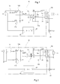
- FIGS 1 and 2 are examples of such types of arrangements.
- Both arrangements shown in figures 1 and 2 include a power stage 10 intended to feed an output voltage to a load L.
- the power stage 10 includes a pair of electronic switches 12a, 12b - typically in the form of power mosfets - which are driven on and off alternatively (see the logic inverter 14 associated to the power switch 12a, in the example shown).
- the two switches in question are connected in a half-bridge arrangement to two capacitors C1, C2 or Cres in order to alternatively connect to an input voltage Vin (having possibly associated an input capacitor Cin, in the layout of figure 2 ) the primary winding T1 of an insulating transformer T.
- the output winding T2 of the transformer T drives via two diodes 16a, 16b the load L via a low pass LC filter 20.
- the primary inductor comprised of the sum of the resonant inductor Lres and leakage inductor Llkg of the transformer T resonates with an output capacitor Cres connected across the secondary winding T2.
- the magnetisizing inductor LM of the transformer T is caused to resonate with the two capacitors Cres associated with the switches 12a and 12b.
- a voltage divider including two resistors R1 and R2 is connected across the load L as a sensor to sense the load L.
- the output signal from the divider R1, R2 is fed (with a negative sign) to a summing node 22 which in turn receives (with a positive sign) a reference voltage Vref.
- the output of the summation node drives a controller.
- the controller includes a voltage controlled oscillator (VCO) 24 whose output drives the electronic switches 12a, 12b.
- VCO 24 is driven by controller unit 26 - e.g. a Proportional/Integral (PI) or Proportional/Integral/Differential (PID) controller.
- PI Proportional/Integral
- PID Proportional/Integral/Differential
- the object of the present invention is to provide such an improved arrangement. According to the invention, that object is achieved by means of an arrangement having the features set forth in the claims that follow.
- the invention also relates to a corresponding method.
- the claims are an integral part of the disclosure of the invention provided herein.
- topologies such as those illustrated in figures 1 and 2 exhibit a voltage gain v. frequency behaviour where, starting from the resonant frequency, the gain (normalised with respect to the starting maximum value) eventually becomes almost flat.
- a constant voltage (e.g. 24 Volt) power supply which currently handles loads between 100% and 10% of the nominal value by varying the frequency between 90KHz and 110KHz may reach an operating frequency of about 200KHz when working at no load. This means that if one causes the system to vary its output even of a small amount, one may obtain a significant variation in the output frequency.
- An embodiment of the improved arrangement described herein is thus based on the concept of injecting a small disturbance at the output side of a device as those illustrated in the foregoing (or any resonant circuit topology based on the same operating principle).
- the disturbance is injected at the point where an output voltage divider provides a feedback signal representative of the output signal to be compared with a reference voltage Vref.
- the disturbance can be generated by a low frequency square wave oscillator that slightly "affects" the voltage feedback, for instance via a diode and a resistor.
- the arrangement described herein provides an effective spread in the EMI spectrum which represents a viable solution to the problem of suppressing any obnoxious interference.
- reference numeral 10 is used to denote the corresponding set of components described in detail with reference to figures 1 and 2 . For that reasons, the various elements included in the blocks labelled 10 in figures 1 and 2 will not be described again.
- R1 denotes the voltage divider arranged at the output of the power stage 10 to provide the feedback signal representative of the output voltage on the load L to be fed back to the summing node 22 to provide (for instance via the PI/PID controller 26 and the VCO 24) the feedback signal towards the electronic switches 12a, 12b.
- the capacitor Cout in the low pass filter 20 (which is in fact included in the block 10) has been represented as a separate element. This was done in order to emphasize the role played by the capacitor Cout in defining, together with the load L, the time constant of the output filter.
- FIG. 3 and 4 Cf schematically denotes the capacitor element(s) included in the integrator of the PI/PID controller 26.
- an oscillator 30 is present which produces a square wave with a period T and a duty cycle of e.g. 50%.
- the square wave is injected (e.g. via a resistor R3 and a diode D1) as a small "disturbance" signal at the partition point of the voltage divider R1, R2.
- the small disturbance signal is a low frequency signal (e.g. 300 Hz): this is substantially lower than the switching frequency at which the switches 12a, 12b are driven - this is typically in the tens of KHz range and as such is the source of EMI.
- This low frequency disturbance signal is thus fed into the feedback loop of the controller and causes the output frequency of the VCO to be correspondingly swept thus producing the desired spreading of the EMI produced by the converter.
- the disturbance injected into the feedback loop via the series connection of the resistor R3 and the diode D1 (and thus the resulting EMI sweep) is non-symmetrical.
- the series connection of the resistor R3 and the diode D1 is connected in parallel to a further resistor R4.
- the values of the resistors R3 and R4 are selected in such a way that the output voltage of the oscillator 30 affects in the same way the feedback voltage during the high and the low state of the oscillator 30. In that way, the disturbance injected into the feedback loop (and the resulting EMI sweep) is symmetrical.
- the impedance Rload exhibited by the load L (a purely resistive value of the load impedance is assumed here for the sake of simplicity) will be high and the time constant of the output filter, namely Rload.Cout, will be larger than the period T of the injected noise.
- the ripple induced on the converter output by the noise injected into the feedback loop will in any case be negligible while producing an effective variation (i.e. spread) of the EMI produced by the switching behaviour of the converter.
- the output voltage will remain constant in the case of a symmetric disturbance being injected (i.e. the embodiment of figure 4 ).
- the voltage will be affected to a very minor amount (e.g. 200 - 300 mV).
- an enable/disable EMI correction switch 32 (which can be either set manually or operated automatically by a circuit sensing the value of the load L) will act on an electronic switch such as a transistor 34 to disable the low frequency oscillator 30 (for instance by a short-circuiting the output thereof).
- a high impedance device 36 such as a conventional three-state buffer is used to disconnect the oscillator 30: in fact, in the case of figure 4 , an arrangement including just the transistor 34 as shown in figure 3 may not produce the desired result because the resistor R4 of the arrangement changes the structure of the voltage divider R1, R2.
- Figure 5 is an example of an arrangement essentially akin to the arrangement of figure 4 in so far the elements R1, R2, Cout, D1, R3 and R4 are concerned.
- FIG. 5 takes into account the possible availability of a microcontroller 38 which may be present in the controller 10 for other purposes (for instance as a part of a dimmer).
- reference 40 denotes a pin of the microcontroller 38 that drives an electronic switch 42 such as e.g. a power mosfet to perform the dimming action proper.
- the function of the oscillator 30 of figures 3 and 4 can be easily obtained by toggling the output of e.g. a three-state logic port 44 of the microcontroller 38, thus producing a PWM output with a duty cycle which can be fixed at 50%.
- the microcontroller 38 will be generally "aware" of the value of the load L, the microcontroller 38 will be in a position to disable the function of the port 44 as an oscillator (for instance by placing the port 44 at a high impedance state).
Landscapes
- Physics & Mathematics (AREA)
- Electromagnetism (AREA)
- Engineering & Computer Science (AREA)
- Power Engineering (AREA)
- Dc-Dc Converters (AREA)
Abstract
Description
- This disclosure relates to reducing electromagnetic interference (EMI).
- The disclosure was devised with specific attention paid to its possible use in reducing EMI as generated e.g. by converters for feeding lighting equipment.
- Power supplies with a variable operating frequency are an experimented approach in solving EMI problems in conjunction with off-line switching power supplies. A variable operating frequency leads to the noise spectrum being spread over a range of frequencies, thus reducing the peak values around a fixed frequency.
- Such an approach is satisfactory in the presence of heavy or medium loads. The input voltage, coming directly from the rectified AC mains voltage or from a PFC (Power Factor Correction) input stage is not perfectly stabilized, and low frequency ripple (100Hz in the case of 50Hz mains as used in Europe) is eliminated by the feedback loop that changes the working frequency in order to keep the output voltage (in the case of constant voltage devices) or the output current (in the case of constant current devices) constant irrespective of input fluctuations. This operation is performed by the switching controller that varies the working frequency so that the device can produce more or less power depending on the load connected thereto.
- For the same reasons, if the input voltage is fixed, but the load changes continuously, for example if the output of the power supply is connected to a low voltage dimmer, the control loop will continuously modify the working frequency in order to keep the output constant.
- The benefits of frequency variation are well visible by observing an EMI spectrum as measured with a spectrum analyzer especially in the range of the "conducted noise" (from 9KHz to 30 MHz for European lighting equipment). These benefits can be best appreciated by comparing two power supplies, the former working with a variable frequency (for example a series resonant converter based on a half-bridge topology), and the latter working at a fixed frequency (for instance, a standard hard-switching half-bridge converter).
- Such an approach may not be satisfactory in the presence of light loads or under "no load" conditions (i.e. little or no current absorption), namely when the dimming level is close to 0% due to a dimming action performed by a dimmer or when the load is completely disconnected. In that case, the input voltage is completely fixed and the input capacitor (which stores the energy during the period - for instance 10ms - of the ac mains input) is only slightly discharged or remains completely charged at the maximum value since the load absorbs only a very small amount of energy to be supplied. This situation also occurs if the device is connected to a dimmer: the switching controller tries to react to the load connection but, in the presence of light load, in order to keep the output stable, it has to produce only a small variation of the working frequency. As a consequence of this, observing the EMI spectrum indicates only a small reduction of the spikes.
- A number of solutions have been proposed in the past to overcome this drawback.
- A first solution involves using large EMI filters operating in the range of the resulting EMI noise.
- While effective, these filters exhibit a number of intrinsic disadvantages, in that they i.a.:
- add to the cost (and thus to the price) of the device,
- increase the size of the device, and
- may strongly decrease the efficiency of the device.
- Another known approach involves using a so-called "bleeder" resistor arranged at the input or the output side of the power supply device. This resistor can be arranged either across the input capacitor or across the output capacitor of the device.
- The bleeder resistor reduces extensively the efficiency in the presence of light loads and may require to be disconnected in the presence of heavy loads to provide acceptable operation. Also, solutions based on a bleeder resistor exhibit further disadvantages such as:
- when no load is connected to the device or the power adsorbed by the load is very small (for instance, when the device is at standby) the bleeder resistor undesirably absorbs power;
- the bleeder resistor inevitably needs to be of relatively high value. To obtain acceptable results (that is, an acceptable frequency variation) a certain amount of power must be dissipated (typically 5-10% of the nominal power); this requires a resistor having a certain size, which reduces the power/volume (Watt/cm3) ratio in the device.
- Still another solution is based on "burst mode" operation: when the working frequency reaches a maximum or minimum limit value (depending on the topology implemented and the working mode) the controller stops for a certain time emitting driving commands to the electronic switches (e.g. power mosfets) in the converter. By adopting this technique, the limit frequency remains the same while the driving commands appear only for a short (usually pre-defined) time. By way of example, if a minimum working frequency of 10KHz is reached, the driving pulses to the mosfets are discontinued. As a consequence, they appear approximately only for 50% of the time. The result is a sort of a mixed pulse-plus-frequency modulation which is intrinsically non-dissipative when compared in terms of efficiency to the solutions considered previously.
- Rather than leading to a spreading of the noise spectrum, "burst mode" operation reduces the EMI noise because the power stages stop for a certain time. The limit frequency is in any case fixed and if this frequency (or a multiple of it) represents the source of noise, it is less "captured" by any device exposed to EMI. This may lead to an improvement, but the noise energy still remains concentrated at a given frequency. So, burst mode operation is unable to solve EMI problems if the device is a small power device (less than 20 Watts) and may be generally unable to solve the problem even for larger powers without resorting to an EMI filter.
- The possibility also exists of reducing the number of pulses in a group thus increasing the burst period by limiting the maximum or minimum frequency to a higher or lower value. This however has the disadvantage of leading to an unacceptable audio noise due to the distance between two consecutive groups of pulses. In fact, the burst period may easily fall into the audio frequency range for which EMI protection is sought.
- Modifications to parallel/series resonant converter topologies may lead, with the addition of a small amount of components, to dispensing with a number of the drawbacks considered in the foregoing, thus leading to arrangements that:
- no longer require the use of (large) EMI filters, thus avoiding any variation in efficiency (especially the starting efficiency) with varying line or load conditions,
- distribute the noise spectrum over a wide range, excepting however the audio frequency range,
- lead to solutions adapted to be implemented with very cheap components.
- These solutions may involve resonant converter arrangements where the primary inductor comprised of the sum of the resonant and the leakage inductor of the insulating transformer resonates with an output resonant capacitor as well as arrangements where the magnetizing inductor of the insulating transformer resonates with two capacitors arranged in parallel.
-
Figures 1 and 2 are examples of such types of arrangements. - Both arrangements shown in
figures 1 and 2 include apower stage 10 intended to feed an output voltage to a load L. - The
power stage 10 includes a pair ofelectronic switches logic inverter 14 associated to thepower switch 12a, in the example shown). The two switches in question are connected in a half-bridge arrangement to two capacitors C1, C2 or Cres in order to alternatively connect to an input voltage Vin (having possibly associated an input capacitor Cin, in the layout offigure 2 ) the primary winding T1 of an insulating transformer T. The output winding T2 of the transformer T drives via twodiodes pass LC filter 20. - In the embodiment of
figure 1 , the primary inductor comprised of the sum of the resonant inductor Lres and leakage inductor Llkg of the transformer T resonates with an output capacitor Cres connected across the secondary winding T2. In the arrangement offigure 2 , the magnetisizing inductor LM of the transformer T is caused to resonate with the two capacitors Cres associated with theswitches - In both
figures 1 and 2 , a voltage divider including two resistors R1 and R2 is connected across the load L as a sensor to sense the load L. The output signal from the divider R1, R2 is fed (with a negative sign) to asumming node 22 which in turn receives (with a positive sign) a reference voltage Vref. - The output of the summation node drives a controller. In the embodiment illustrated, the controller includes a voltage controlled oscillator (VCO) 24 whose output drives the
electronic switches - The preceding description indicates that the need is felt for improved arrangements to dispense with the drawbacks intrinsic to the various arrangements discussed in the foregoing.
- The object of the present invention is to provide such an improved arrangement. According to the invention, that object is achieved by means of an arrangement having the features set forth in the claims that follow. The invention also relates to a corresponding method. The claims are an integral part of the disclosure of the invention provided herein.
- In brief, the inventors have noted that topologies such as those illustrated in
figures 1 and 2 (and, generally, any arrangement including a switched power supply with a sensor for sensing a load fed by the power supply and a feedback path controlling the switching frequency of the switched power supply as a function of the load) exhibit a voltage gain v. frequency behaviour where, starting from the resonant frequency, the gain (normalised with respect to the starting maximum value) eventually becomes almost flat. For instance, a constant voltage (e.g. 24 Volt) power supply which currently handles loads between 100% and 10% of the nominal value by varying the frequency between 90KHz and 110KHz may reach an operating frequency of about 200KHz when working at no load. This means that if one causes the system to vary its output even of a small amount, one may obtain a significant variation in the output frequency. - An embodiment of the improved arrangement described herein is thus based on the concept of injecting a small disturbance at the output side of a device as those illustrated in the foregoing (or any resonant circuit topology based on the same operating principle). In an embodiment, the disturbance is injected at the point where an output voltage divider provides a feedback signal representative of the output signal to be compared with a reference voltage Vref.
- In an embodiment, the disturbance can be generated by a low frequency square wave oscillator that slightly "affects" the voltage feedback, for instance via a diode and a resistor.
- The arrangement described herein provides an effective spread in the EMI spectrum which represents a viable solution to the problem of suppressing any obnoxious interference.
- Experiments carried out by the applicant indicate that a disturbance with a frequency in the range 100 Hz - 1KHz with an amplitude of the order of 2-3% of the output voltage is effective in generating a satisfactory spread in the EMI spectrum.
- These values (and especially the frequency) may be properly adapted depending on the specific operational needs.
- The invention will now be described, by way of example only, with reference to the annexed views, wherein:
-
figures 1 and 2 have already been discussed in the foregoing, -
figure 3 is illustrative of a first embodiment of the arrangement described herein, -
figure 4 is illustrative of a second embodiment of the arrangement described herein, and -
figure 5 is illustrative of a third embodiment of the arrangement described herein. - In the following description, numerous specific details are given to provide a thorough understanding of embodiments. The embodiments can be practiced without one or more of the specific details, or with other methods, components, materials, etc. In other instances, well-known structures, materials, or operations are not shown or described in detail to avoid obscuring aspects of the embodiments.
- Reference throughout this specification to "one embodiment" or "an embodiment" means that a particular feature, structure, or characteristic described in connection with the embodiment is included in at least one embodiment. Thus, the appearances of the phrases "in one embodiment" or "in an embodiment" in various places throughout this specification are not necessarily all referring to the same embodiment. Furthermore, the particular features, structures, or characteristics may be combined in any suitable manner in one or more embodiments.
- The headings provided herein are for convenience only and do not interpret the scope or meaning of the embodiments.
- Throughout
figures 3 to 5 ,reference numeral 10 is used to denote the corresponding set of components described in detail with reference tofigures 1 and 2 . For that reasons, the various elements included in the blocks labelled 10 infigures 1 and 2 will not be described again. - This schematic representation (as used in
figures 3 to 5 ) is representative of the fact that the arrangement described herein may be applied also to converter arrangements that do not correspond exactly to those exemplified infigures 1 and 2 , provided these are based on the same operating principles. - It will be appreciated that throughout
figures 3 to 5 R1, R2 denotes the voltage divider arranged at the output of thepower stage 10 to provide the feedback signal representative of the output voltage on the load L to be fed back to the summingnode 22 to provide (for instance via the PI/PID controller 26 and the VCO 24) the feedback signal towards theelectronic switches - In
figures 3 to 5 , the capacitor Cout in the low pass filter 20 (which is in fact included in the block 10) has been represented as a separate element. This was done in order to emphasize the role played by the capacitor Cout in defining, together with the load L, the time constant of the output filter. - In
figures 3 and 4 Cf schematically denotes the capacitor element(s) included in the integrator of the PI/PID controller 26. - In both embodiments of
figures 3 and 4 , anoscillator 30 is present which produces a square wave with a period T and a duty cycle of e.g. 50%. The square wave is injected (e.g. via a resistor R3 and a diode D1) as a small "disturbance" signal at the partition point of the voltage divider R1, R2. The small disturbance signal is a low frequency signal (e.g. 300 Hz): this is substantially lower than the switching frequency at which theswitches - This low frequency disturbance signal is thus fed into the feedback loop of the controller and causes the output frequency of the VCO to be correspondingly swept thus producing the desired spreading of the EMI produced by the converter.
- In the embodiment of
figure 3 , the disturbance injected into the feedback loop via the series connection of the resistor R3 and the diode D1 (and thus the resulting EMI sweep) is non-symmetrical. - In the embodiment of
figure 4 the series connection of the resistor R3 and the diode D1 is connected in parallel to a further resistor R4. The values of the resistors R3 and R4 are selected in such a way that the output voltage of theoscillator 30 affects in the same way the feedback voltage during the high and the low state of theoscillator 30. In that way, the disturbance injected into the feedback loop (and the resulting EMI sweep) is symmetrical. - In the presence of a light load - i.e. low current absorption - the impedance Rload exhibited by the load L (a purely resistive value of the load impedance is assumed here for the sake of simplicity) will be high and the time constant of the output filter, namely Rload.Cout, will be larger than the period T of the injected noise. In these conditions the ripple induced on the converter output by the noise injected into the feedback loop will in any case be negligible while producing an effective variation (i.e. spread) of the EMI produced by the switching behaviour of the converter.
- Specifically, the output voltage will remain constant in the case of a symmetric disturbance being injected (i.e. the embodiment of
figure 4 ). In the case of an asymmetric disturbance, the voltage will be affected to a very minor amount (e.g. 200 - 300 mV). - In the presence of a "heavy" load - i.e. high current absorption - the fluctuations can be visible and thus not acceptable.
- For that reason, an enable/disable EMI correction switch 32 (which can be either set manually or operated automatically by a circuit sensing the value of the load L) will act on an electronic switch such as a
transistor 34 to disable the low frequency oscillator 30 (for instance by a short-circuiting the output thereof). - In the embodiment of
figure 4 , ahigh impedance device 36 such as a conventional three-state buffer is used to disconnect the oscillator 30: in fact, in the case offigure 4 , an arrangement including just thetransistor 34 as shown infigure 3 may not produce the desired result because the resistor R4 of the arrangement changes the structure of the voltage divider R1, R2. -
Figure 5 is an example of an arrangement essentially akin to the arrangement offigure 4 in so far the elements R1, R2, Cout, D1, R3 and R4 are concerned. - The arrangement of
figure 5 takes into account the possible availability of amicrocontroller 38 which may be present in thecontroller 10 for other purposes (for instance as a part of a dimmer). In the block diagram offigure 5 reference 40 denotes a pin of themicrocontroller 38 that drives anelectronic switch 42 such as e.g. a power mosfet to perform the dimming action proper. - In such a case, the function of the
oscillator 30 offigures 3 and 4 can be easily obtained by toggling the output of e.g. a three-state logic port 44 of themicrocontroller 38, thus producing a PWM output with a duty cycle which can be fixed at 50%. - As the
microcontroller 38 will be generally "aware" of the value of the load L, themicrocontroller 38 will be in a position to disable the function of theport 44 as an oscillator (for instance by placing theport 44 at a high impedance state). - Experiments carried out by the applicant have demonstrated satisfactory operation of the arrangement of
figure 5 in the case of a power supply with integrated dimmer and two-wire digital interface (TX-RX). Such an arrangement has been tested under "no load" conditions first without applying any EMI correction, then applying a non-symmetrical disturbance (according to the basic layout offigure 3 ) obtained from a 300 Hz, 50% duty cycle square wave. This was used to create a small perturbation at the feedback node of the power stage (output resistor divider R1, R2). In the specific experimental arrangement tested a value of 23.7 KOhm was selected for the resistor R3. Vout was 24 volt and the reference voltage was 2.5 volt. R1 was selected at 2.7 KOhm and R2 was selected at 47 Kohm. The square wave amplitude was 3.3 volts and the current coming from the feedback resistor R2 was about 900µA, while the current coming from the compensation circuit was about 10µA i.e. 1.1% of the feedback current. - By using such an arrangement an effective spread of EMI noise over the range 0.15 to 3 MHz was observed. This is considered acceptable for a wide range of applications related to lighting equipment.
- Without prejudice to the underlying principles of the invention, the details and embodiments may vary, even significantly, with respect to what has been described herein by way of example only, without departing from the scope of the invention as defined in the annexed claims.
Claims (12)
- A circuit arrangement for reducing electromagnetic interference from a switched power supply (10) including a sensor (R1, R2) to sense a load (L) fed by the power supply (10) and a feedback path (22, 24, 26) to control the switching frequency of the switched power supply (10) as a function of said load (L) as sensed by said sensor (R1, R2), the arrangement including an oscillator (30, 38) to inject into said feedback path (22, 24, 26) an oscillating signal, said oscillating signal producing a spread in the spectrum of the electromagnetic noise produced by the switched power supply (10).
- The circuit of Claim 1, wherein said oscillating signal is a low frequency signal having a frequency substantially lower than the switching frequency of said switched power supply (10).
- The circuit of either of Claims 1 or 2, including a switch (34, 36) to selectively switch off said oscillating signal to prevent fluctuations in the output of said power supply (10).
- The circuit of any of the preceding claims, wherein said oscillator (30, 38) is a square wave oscillator.
- The circuit of any of the preceding claims, wherein said oscillator (30, 38) produces an oscillating signal in the form of 50% duty cycle square wave.
- The circuit of any of the preceding claims, wherein said oscillator (30) injects into said feedback path (22, 24, 26) an oscillating signal with a non-symmetrical waveform.
- The circuit of claim 6, wherein said oscillator (30) is coupled to said feedback path (22, 24, 26) via a resistor (R3) and a diode (D1).
- The circuit of any of claims 1 to 5, wherein said oscillator (30) injects into said feedback path (22, 24, 26) an oscillating signal with a symmetrical waveform.
- The circuit of claim 8, wherein said oscillator (30) is coupled to said feedback path (22, 24, 26) via the parallel connection of:- the series connection of a resistor (R3) and a diode (D1); and- a further resistor (R4).
- The circuit of any of the preceding claims, wherein said sensor is a voltage divider (R1, R2).
- The circuit of any of the preceding claims, wherein said oscillator is included in a microcontroller (38) associated with said power supply (10).
- A method of reducing electromagnetic interference from a switched power supply (10) including sensing (R1, R2) a load (L) fed by the power supply (10) and controlling via a feedback path (22, 24, 26) the switching frequency of the switched power supply (10) as a function of said load (L) as sensed, the method including injecting into said feedback path (22, 24, 26) an oscillating signal, said oscillating signal producing a spread in the spectrum of the electromagnetic noise produced by the switched power supply (10).
Priority Applications (4)
| Application Number | Priority Date | Filing Date | Title |
|---|---|---|---|
| EP08162315A EP2154771B1 (en) | 2008-08-13 | 2008-08-13 | Circuit and method for reducing electromagnetic interference |
| AT08162315T ATE531119T1 (en) | 2008-08-13 | 2008-08-13 | CIRCUIT AND METHOD FOR REDUCING ELECTROMAGNETIC INTERFERENCE |
| KR1020090073712A KR20100020914A (en) | 2008-08-13 | 2009-08-11 | Circuit and method for reducing electromagnetic interference |
| CN200910164861.2A CN101651410B (en) | 2008-08-13 | 2009-08-11 | Circuits and methods for reducing electromagnetic interference |
Applications Claiming Priority (1)
| Application Number | Priority Date | Filing Date | Title |
|---|---|---|---|
| EP08162315A EP2154771B1 (en) | 2008-08-13 | 2008-08-13 | Circuit and method for reducing electromagnetic interference |
Publications (2)
| Publication Number | Publication Date |
|---|---|
| EP2154771A1 true EP2154771A1 (en) | 2010-02-17 |
| EP2154771B1 EP2154771B1 (en) | 2011-10-26 |
Family
ID=40214590
Family Applications (1)
| Application Number | Title | Priority Date | Filing Date |
|---|---|---|---|
| EP08162315A Active EP2154771B1 (en) | 2008-08-13 | 2008-08-13 | Circuit and method for reducing electromagnetic interference |
Country Status (4)
| Country | Link |
|---|---|
| EP (1) | EP2154771B1 (en) |
| KR (1) | KR20100020914A (en) |
| CN (1) | CN101651410B (en) |
| AT (1) | ATE531119T1 (en) |
Cited By (4)
| Publication number | Priority date | Publication date | Assignee | Title |
|---|---|---|---|---|
| US9148052B2 (en) | 2011-03-23 | 2015-09-29 | Samsung Electronics Co., Ltd. | Switching regulator with reduced EMI |
| DE102015202245A1 (en) * | 2015-02-09 | 2016-08-11 | Tridonic Gmbh & Co Kg | Down converter with frequency modulated switch control |
| EP2503695A3 (en) * | 2011-03-24 | 2016-12-07 | LG Innotek Co., Ltd. | A circuit for mitigating electromagnetic interference in input stage of a driver IC |
| AT15401U1 (en) * | 2012-12-28 | 2017-08-15 | Tridonic Gmbh & Co Kg | Operation of bulbs with a resonant converter |
Families Citing this family (3)
| Publication number | Priority date | Publication date | Assignee | Title |
|---|---|---|---|---|
| US9203293B2 (en) * | 2012-06-11 | 2015-12-01 | Power Systems Technologies Ltd. | Method of suppressing electromagnetic interference emission |
| US9203292B2 (en) * | 2012-06-11 | 2015-12-01 | Power Systems Technologies Ltd. | Electromagnetic interference emission suppressor |
| JP6497144B2 (en) * | 2015-03-13 | 2019-04-10 | 富士電機株式会社 | Switching power supply control circuit and switching power supply |
Citations (3)
| Publication number | Priority date | Publication date | Assignee | Title |
|---|---|---|---|---|
| US5640315A (en) * | 1994-03-18 | 1997-06-17 | Nippon Steel Corporation | Switching regulator |
| US20050110473A1 (en) * | 2003-11-20 | 2005-05-26 | Nakada Mitsuo | Switching signal modulation circuit |
| EP1791399A1 (en) * | 2005-11-22 | 2007-05-30 | Patent-Treuhand-Gesellschaft für elektrische Glühlampen mbH | A LED driving arrangement |
Family Cites Families (1)
| Publication number | Priority date | Publication date | Assignee | Title |
|---|---|---|---|---|
| JP2007043565A (en) * | 2005-08-04 | 2007-02-15 | Fuji Electric Holdings Co Ltd | Signal transmission method |
-
2008
- 2008-08-13 AT AT08162315T patent/ATE531119T1/en not_active IP Right Cessation
- 2008-08-13 EP EP08162315A patent/EP2154771B1/en active Active
-
2009
- 2009-08-11 CN CN200910164861.2A patent/CN101651410B/en not_active Expired - Fee Related
- 2009-08-11 KR KR1020090073712A patent/KR20100020914A/en not_active Ceased
Patent Citations (3)
| Publication number | Priority date | Publication date | Assignee | Title |
|---|---|---|---|---|
| US5640315A (en) * | 1994-03-18 | 1997-06-17 | Nippon Steel Corporation | Switching regulator |
| US20050110473A1 (en) * | 2003-11-20 | 2005-05-26 | Nakada Mitsuo | Switching signal modulation circuit |
| EP1791399A1 (en) * | 2005-11-22 | 2007-05-30 | Patent-Treuhand-Gesellschaft für elektrische Glühlampen mbH | A LED driving arrangement |
Non-Patent Citations (1)
| Title |
|---|
| SANTOLARIA A ET AL: "EMI reduction in switched power converters by means of spread spectrum modulation techniques", POWER ELECTRONICS SPECIALISTS CONFERENCE, 2004. PESC 04. 2004 IEEE 35T H ANNUAL AACHEN, GERMANY 20-25 JUNE 2004, PISCATAWAY, NJ, USA,IEEE, US, 20 June 2004 (2004-06-20), pages 292 - 296Vol.1, XP010738006, ISBN: 978-0-7803-8399-9 * |
Cited By (5)
| Publication number | Priority date | Publication date | Assignee | Title |
|---|---|---|---|---|
| US9148052B2 (en) | 2011-03-23 | 2015-09-29 | Samsung Electronics Co., Ltd. | Switching regulator with reduced EMI |
| EP2503695A3 (en) * | 2011-03-24 | 2016-12-07 | LG Innotek Co., Ltd. | A circuit for mitigating electromagnetic interference in input stage of a driver IC |
| AT15401U1 (en) * | 2012-12-28 | 2017-08-15 | Tridonic Gmbh & Co Kg | Operation of bulbs with a resonant converter |
| DE102015202245A1 (en) * | 2015-02-09 | 2016-08-11 | Tridonic Gmbh & Co Kg | Down converter with frequency modulated switch control |
| DE102015202245B4 (en) * | 2015-02-09 | 2024-09-19 | Tridonic Gmbh & Co Kg | Step-down converter with frequency modulated switch control |
Also Published As
| Publication number | Publication date |
|---|---|
| EP2154771B1 (en) | 2011-10-26 |
| KR20100020914A (en) | 2010-02-23 |
| ATE531119T1 (en) | 2011-11-15 |
| CN101651410B (en) | 2014-05-21 |
| CN101651410A (en) | 2010-02-17 |
Similar Documents
| Publication | Publication Date | Title |
|---|---|---|
| US8581518B2 (en) | Triac dimmer compatible switching mode power supply and method thereof | |
| CN112117890B (en) | Switching power supply control circuit and method | |
| CN102282522B (en) | Improved Linearity in LED Dimming Control | |
| CN102203690B (en) | Current ripple reduction circuit for leds | |
| US20100207536A1 (en) | High efficiency light source with integrated ballast | |
| CN102273327B (en) | Dimmer-controlled LEDs using flyback converter with high power factor | |
| RU2427953C2 (en) | Adaptive circuit for control of conversion circuit | |
| TWI442676B (en) | Dimmer control leakage pull down using main power device in flyback converter | |
| JP4474562B2 (en) | Light emitting diode drive device | |
| RU2479955C2 (en) | Device and method of lighting based on led with high capacity ratio | |
| US7990070B2 (en) | LED power source and DC-DC converter | |
| EP2154771B1 (en) | Circuit and method for reducing electromagnetic interference | |
| CN105703640A (en) | Control method and device employing primary side regulation in a quasi-resonant ac/dc flyback converter | |
| CN101347046B (en) | LED driver | |
| CN201839477U (en) | LED drive circuit and lamp | |
| EP1580638A1 (en) | Transition mode power factor correction device in switching power supplies | |
| US7019988B2 (en) | Switching-type power converter | |
| CN104349550A (en) | Solid state lighting control | |
| TW201301936A (en) | A cascade boost and inverting buck converter with independent control | |
| CN102573208B (en) | Dimming device and lighting apparatus using same | |
| KR100952920B1 (en) | Single Stage LED Driver | |
| CN113661784B (en) | Converter for driving load, LED driver and LED lighting device | |
| Moriconi | Designing a high power factor switching preregulator with the L4981 continuous mode | |
| KR19980059503U (en) | EL lamp power supply. |
Legal Events
| Date | Code | Title | Description |
|---|---|---|---|
| PUAI | Public reference made under article 153(3) epc to a published international application that has entered the european phase |
Free format text: ORIGINAL CODE: 0009012 |
|
| AK | Designated contracting states |
Kind code of ref document: A1 Designated state(s): AT BE BG CH CY CZ DE DK EE ES FI FR GB GR HR HU IE IS IT LI LT LU LV MC MT NL NO PL PT RO SE SI SK TR |
|
| AX | Request for extension of the european patent |
Extension state: AL BA MK RS |
|
| 17P | Request for examination filed |
Effective date: 20100726 |
|
| AKX | Designation fees paid |
Designated state(s): AT BE BG CH CY CZ DE DK EE ES FI FR GB GR HR HU IE IS IT LI LT LU LV MC MT NL NO PL PT RO SE SI SK TR |
|
| GRAP | Despatch of communication of intention to grant a patent |
Free format text: ORIGINAL CODE: EPIDOSNIGR1 |
|
| GRAS | Grant fee paid |
Free format text: ORIGINAL CODE: EPIDOSNIGR3 |
|
| RAP1 | Party data changed (applicant data changed or rights of an application transferred) |
Owner name: OSRAM AG Owner name: OSRAM S.P.A. - SOCIETA' RIUNITE OSRAM EDISON CLERI |
|
| GRAA | (expected) grant |
Free format text: ORIGINAL CODE: 0009210 |
|
| AK | Designated contracting states |
Kind code of ref document: B1 Designated state(s): AT BE BG CH CY CZ DE DK EE ES FI FR GB GR HR HU IE IS IT LI LT LU LV MC MT NL NO PL PT RO SE SI SK TR |
|
| REG | Reference to a national code |
Ref country code: GB Ref legal event code: FG4D |
|
| REG | Reference to a national code |
Ref country code: CH Ref legal event code: EP |
|
| REG | Reference to a national code |
Ref country code: IE Ref legal event code: FG4D |
|
| REG | Reference to a national code |
Ref country code: DE Ref legal event code: R096 Ref document number: 602008010780 Country of ref document: DE Effective date: 20120105 |
|
| REG | Reference to a national code |
Ref country code: NL Ref legal event code: VDEP Effective date: 20111026 |
|
| LTIE | Lt: invalidation of european patent or patent extension |
Effective date: 20111026 |
|
| REG | Reference to a national code |
Ref country code: AT Ref legal event code: MK05 Ref document number: 531119 Country of ref document: AT Kind code of ref document: T Effective date: 20111026 |
|
| PG25 | Lapsed in a contracting state [announced via postgrant information from national office to epo] |
Ref country code: IS Free format text: LAPSE BECAUSE OF FAILURE TO SUBMIT A TRANSLATION OF THE DESCRIPTION OR TO PAY THE FEE WITHIN THE PRESCRIBED TIME-LIMIT Effective date: 20120226 Ref country code: LT Free format text: LAPSE BECAUSE OF FAILURE TO SUBMIT A TRANSLATION OF THE DESCRIPTION OR TO PAY THE FEE WITHIN THE PRESCRIBED TIME-LIMIT Effective date: 20111026 Ref country code: BE Free format text: LAPSE BECAUSE OF FAILURE TO SUBMIT A TRANSLATION OF THE DESCRIPTION OR TO PAY THE FEE WITHIN THE PRESCRIBED TIME-LIMIT Effective date: 20111026 Ref country code: NO Free format text: LAPSE BECAUSE OF FAILURE TO SUBMIT A TRANSLATION OF THE DESCRIPTION OR TO PAY THE FEE WITHIN THE PRESCRIBED TIME-LIMIT Effective date: 20120126 |
|
| PG25 | Lapsed in a contracting state [announced via postgrant information from national office to epo] |
Ref country code: LV Free format text: LAPSE BECAUSE OF FAILURE TO SUBMIT A TRANSLATION OF THE DESCRIPTION OR TO PAY THE FEE WITHIN THE PRESCRIBED TIME-LIMIT Effective date: 20111026 Ref country code: SE Free format text: LAPSE BECAUSE OF FAILURE TO SUBMIT A TRANSLATION OF THE DESCRIPTION OR TO PAY THE FEE WITHIN THE PRESCRIBED TIME-LIMIT Effective date: 20111026 Ref country code: PL Free format text: LAPSE BECAUSE OF FAILURE TO SUBMIT A TRANSLATION OF THE DESCRIPTION OR TO PAY THE FEE WITHIN THE PRESCRIBED TIME-LIMIT Effective date: 20111026 Ref country code: GR Free format text: LAPSE BECAUSE OF FAILURE TO SUBMIT A TRANSLATION OF THE DESCRIPTION OR TO PAY THE FEE WITHIN THE PRESCRIBED TIME-LIMIT Effective date: 20120127 Ref country code: SI Free format text: LAPSE BECAUSE OF FAILURE TO SUBMIT A TRANSLATION OF THE DESCRIPTION OR TO PAY THE FEE WITHIN THE PRESCRIBED TIME-LIMIT Effective date: 20111026 Ref country code: NL Free format text: LAPSE BECAUSE OF FAILURE TO SUBMIT A TRANSLATION OF THE DESCRIPTION OR TO PAY THE FEE WITHIN THE PRESCRIBED TIME-LIMIT Effective date: 20111026 Ref country code: PT Free format text: LAPSE BECAUSE OF FAILURE TO SUBMIT A TRANSLATION OF THE DESCRIPTION OR TO PAY THE FEE WITHIN THE PRESCRIBED TIME-LIMIT Effective date: 20120227 Ref country code: HR Free format text: LAPSE BECAUSE OF FAILURE TO SUBMIT A TRANSLATION OF THE DESCRIPTION OR TO PAY THE FEE WITHIN THE PRESCRIBED TIME-LIMIT Effective date: 20111026 |
|
| PG25 | Lapsed in a contracting state [announced via postgrant information from national office to epo] |
Ref country code: CY Free format text: LAPSE BECAUSE OF FAILURE TO SUBMIT A TRANSLATION OF THE DESCRIPTION OR TO PAY THE FEE WITHIN THE PRESCRIBED TIME-LIMIT Effective date: 20111026 |
|
| PG25 | Lapsed in a contracting state [announced via postgrant information from national office to epo] |
Ref country code: SK Free format text: LAPSE BECAUSE OF FAILURE TO SUBMIT A TRANSLATION OF THE DESCRIPTION OR TO PAY THE FEE WITHIN THE PRESCRIBED TIME-LIMIT Effective date: 20111026 Ref country code: DK Free format text: LAPSE BECAUSE OF FAILURE TO SUBMIT A TRANSLATION OF THE DESCRIPTION OR TO PAY THE FEE WITHIN THE PRESCRIBED TIME-LIMIT Effective date: 20111026 Ref country code: EE Free format text: LAPSE BECAUSE OF FAILURE TO SUBMIT A TRANSLATION OF THE DESCRIPTION OR TO PAY THE FEE WITHIN THE PRESCRIBED TIME-LIMIT Effective date: 20111026 Ref country code: BG Free format text: LAPSE BECAUSE OF FAILURE TO SUBMIT A TRANSLATION OF THE DESCRIPTION OR TO PAY THE FEE WITHIN THE PRESCRIBED TIME-LIMIT Effective date: 20120126 Ref country code: CZ Free format text: LAPSE BECAUSE OF FAILURE TO SUBMIT A TRANSLATION OF THE DESCRIPTION OR TO PAY THE FEE WITHIN THE PRESCRIBED TIME-LIMIT Effective date: 20111026 |
|
| PG25 | Lapsed in a contracting state [announced via postgrant information from national office to epo] |
Ref country code: RO Free format text: LAPSE BECAUSE OF FAILURE TO SUBMIT A TRANSLATION OF THE DESCRIPTION OR TO PAY THE FEE WITHIN THE PRESCRIBED TIME-LIMIT Effective date: 20111026 Ref country code: IT Free format text: LAPSE BECAUSE OF FAILURE TO SUBMIT A TRANSLATION OF THE DESCRIPTION OR TO PAY THE FEE WITHIN THE PRESCRIBED TIME-LIMIT Effective date: 20111026 |
|
| PLBE | No opposition filed within time limit |
Free format text: ORIGINAL CODE: 0009261 |
|
| STAA | Information on the status of an ep patent application or granted ep patent |
Free format text: STATUS: NO OPPOSITION FILED WITHIN TIME LIMIT |
|
| 26N | No opposition filed |
Effective date: 20120727 |
|
| REG | Reference to a national code |
Ref country code: DE Ref legal event code: R097 Ref document number: 602008010780 Country of ref document: DE Effective date: 20120727 |
|
| PG25 | Lapsed in a contracting state [announced via postgrant information from national office to epo] |
Ref country code: AT Free format text: LAPSE BECAUSE OF FAILURE TO SUBMIT A TRANSLATION OF THE DESCRIPTION OR TO PAY THE FEE WITHIN THE PRESCRIBED TIME-LIMIT Effective date: 20111026 |
|
| REG | Reference to a national code |
Ref country code: CH Ref legal event code: PL Ref country code: DE Ref legal event code: R081 Ref document number: 602008010780 Country of ref document: DE Owner name: OSRAM GMBH, DE Free format text: FORMER OWNER: OSRAM AG, 81543 MUENCHEN, DE Effective date: 20130205 |
|
| PG25 | Lapsed in a contracting state [announced via postgrant information from national office to epo] |
Ref country code: MC Free format text: LAPSE BECAUSE OF NON-PAYMENT OF DUE FEES Effective date: 20120831 |
|
| PG25 | Lapsed in a contracting state [announced via postgrant information from national office to epo] |
Ref country code: ES Free format text: LAPSE BECAUSE OF FAILURE TO SUBMIT A TRANSLATION OF THE DESCRIPTION OR TO PAY THE FEE WITHIN THE PRESCRIBED TIME-LIMIT Effective date: 20120206 Ref country code: LI Free format text: LAPSE BECAUSE OF NON-PAYMENT OF DUE FEES Effective date: 20120831 Ref country code: CH Free format text: LAPSE BECAUSE OF NON-PAYMENT OF DUE FEES Effective date: 20120831 |
|
| REG | Reference to a national code |
Ref country code: IE Ref legal event code: MM4A |
|
| PG25 | Lapsed in a contracting state [announced via postgrant information from national office to epo] |
Ref country code: FI Free format text: LAPSE BECAUSE OF FAILURE TO SUBMIT A TRANSLATION OF THE DESCRIPTION OR TO PAY THE FEE WITHIN THE PRESCRIBED TIME-LIMIT Effective date: 20111026 |
|
| PG25 | Lapsed in a contracting state [announced via postgrant information from national office to epo] |
Ref country code: IE Free format text: LAPSE BECAUSE OF NON-PAYMENT OF DUE FEES Effective date: 20120813 |
|
| REG | Reference to a national code |
Ref country code: DE Ref legal event code: R081 Ref document number: 602008010780 Country of ref document: DE Owner name: OSRAM GMBH, DE Free format text: FORMER OWNER: OSRAM GMBH, 81543 MUENCHEN, DE Effective date: 20130823 |
|
| PG25 | Lapsed in a contracting state [announced via postgrant information from national office to epo] |
Ref country code: MT Free format text: LAPSE BECAUSE OF FAILURE TO SUBMIT A TRANSLATION OF THE DESCRIPTION OR TO PAY THE FEE WITHIN THE PRESCRIBED TIME-LIMIT Effective date: 20111026 |
|
| PG25 | Lapsed in a contracting state [announced via postgrant information from national office to epo] |
Ref country code: TR Free format text: LAPSE BECAUSE OF FAILURE TO SUBMIT A TRANSLATION OF THE DESCRIPTION OR TO PAY THE FEE WITHIN THE PRESCRIBED TIME-LIMIT Effective date: 20111026 |
|
| PG25 | Lapsed in a contracting state [announced via postgrant information from national office to epo] |
Ref country code: LU Free format text: LAPSE BECAUSE OF NON-PAYMENT OF DUE FEES Effective date: 20120813 |
|
| PG25 | Lapsed in a contracting state [announced via postgrant information from national office to epo] |
Ref country code: HU Free format text: LAPSE BECAUSE OF FAILURE TO SUBMIT A TRANSLATION OF THE DESCRIPTION OR TO PAY THE FEE WITHIN THE PRESCRIBED TIME-LIMIT Effective date: 20080813 |
|
| PGFP | Annual fee paid to national office [announced via postgrant information from national office to epo] |
Ref country code: FR Payment date: 20140821 Year of fee payment: 7 Ref country code: GB Payment date: 20140820 Year of fee payment: 7 |
|
| GBPC | Gb: european patent ceased through non-payment of renewal fee |
Effective date: 20150813 |
|
| REG | Reference to a national code |
Ref country code: FR Ref legal event code: ST Effective date: 20160429 |
|
| PG25 | Lapsed in a contracting state [announced via postgrant information from national office to epo] |
Ref country code: GB Free format text: LAPSE BECAUSE OF NON-PAYMENT OF DUE FEES Effective date: 20150813 |
|
| PG25 | Lapsed in a contracting state [announced via postgrant information from national office to epo] |
Ref country code: FR Free format text: LAPSE BECAUSE OF NON-PAYMENT OF DUE FEES Effective date: 20150831 |
|
| REG | Reference to a national code |
Ref country code: DE Ref legal event code: R081 Ref document number: 602008010780 Country of ref document: DE Owner name: INVENTRONICS GMBH, DE Free format text: FORMER OWNER: OSRAM GMBH, 80807 MUENCHEN, DE Ref country code: DE Ref legal event code: R081 Ref document number: 602008010780 Country of ref document: DE Owner name: OPTOTRONIC GMBH, DE Free format text: FORMER OWNER: OSRAM GMBH, 80807 MUENCHEN, DE |
|
| REG | Reference to a national code |
Ref country code: DE Ref legal event code: R081 Ref document number: 602008010780 Country of ref document: DE Owner name: INVENTRONICS GMBH, DE Free format text: FORMER OWNER: OPTOTRONIC GMBH, 85748 GARCHING, DE |
|
| PGFP | Annual fee paid to national office [announced via postgrant information from national office to epo] |
Ref country code: DE Payment date: 20250819 Year of fee payment: 18 |