EP2154717A2 - Materials for adhesion enhancement of copper film on diffusion barriers - Google Patents
Materials for adhesion enhancement of copper film on diffusion barriers Download PDFInfo
- Publication number
- EP2154717A2 EP2154717A2 EP09167949A EP09167949A EP2154717A2 EP 2154717 A2 EP2154717 A2 EP 2154717A2 EP 09167949 A EP09167949 A EP 09167949A EP 09167949 A EP09167949 A EP 09167949A EP 2154717 A2 EP2154717 A2 EP 2154717A2
- Authority
- EP
- European Patent Office
- Prior art keywords
- carbon atoms
- layer
- groups
- chromium
- group
- Prior art date
- Legal status (The legal status is an assumption and is not a legal conclusion. Google has not performed a legal analysis and makes no representation as to the accuracy of the status listed.)
- Withdrawn
Links
Images


Classifications
-
- H—ELECTRICITY
- H01—ELECTRIC ELEMENTS
- H01L—SEMICONDUCTOR DEVICES NOT COVERED BY CLASS H10
- H01L21/00—Processes or apparatus adapted for the manufacture or treatment of semiconductor or solid state devices or of parts thereof
- H01L21/70—Manufacture or treatment of devices consisting of a plurality of solid state components formed in or on a common substrate or of parts thereof; Manufacture of integrated circuit devices or of parts thereof
- H01L21/71—Manufacture of specific parts of devices defined in group H01L21/70
- H01L21/768—Applying interconnections to be used for carrying current between separate components within a device comprising conductors and dielectrics
- H01L21/76838—Applying interconnections to be used for carrying current between separate components within a device comprising conductors and dielectrics characterised by the formation and the after-treatment of the conductors
- H01L21/76841—Barrier, adhesion or liner layers
- H01L21/76843—Barrier, adhesion or liner layers formed in openings in a dielectric
- H01L21/76846—Layer combinations
-
- H—ELECTRICITY
- H01—ELECTRIC ELEMENTS
- H01L—SEMICONDUCTOR DEVICES NOT COVERED BY CLASS H10
- H01L21/00—Processes or apparatus adapted for the manufacture or treatment of semiconductor or solid state devices or of parts thereof
- H01L21/02—Manufacture or treatment of semiconductor devices or of parts thereof
- H01L21/04—Manufacture or treatment of semiconductor devices or of parts thereof the devices having at least one potential-jump barrier or surface barrier, e.g. PN junction, depletion layer or carrier concentration layer
- H01L21/18—Manufacture or treatment of semiconductor devices or of parts thereof the devices having at least one potential-jump barrier or surface barrier, e.g. PN junction, depletion layer or carrier concentration layer the devices having semiconductor bodies comprising elements of Group IV of the Periodic System or AIIIBV compounds with or without impurities, e.g. doping materials
- H01L21/28—Manufacture of electrodes on semiconductor bodies using processes or apparatus not provided for in groups H01L21/20 - H01L21/268
-
- C—CHEMISTRY; METALLURGY
- C22—METALLURGY; FERROUS OR NON-FERROUS ALLOYS; TREATMENT OF ALLOYS OR NON-FERROUS METALS
- C22C—ALLOYS
- C22C1/00—Making non-ferrous alloys
Definitions
- US 6271131 discloses a method of forming a rhodium (Rh) containing layer such as platinum-rhodium (Pt-Rh) alloy as diffusion barrier via chemical vapor deposition.
- Rh rhodium
- Pt-Rh platinum-rhodium
- Ti-Ta titanium-tantalum
- the Ti rich/Ta deficient portion provides good adhesion to the dielectric film and the Ta rich/Ti deficient portion forms a hetero-epitaxial interface with the interconnect film and suppresses the formation of intermetallic compounds.
- US 5942799 discloses a multilayer diffusion barrier comprising a refractory metal such as tungsten (W), titanium (Ti), tantalum (Ta), molybdenum (Mo); and a refractory metal nitride such as WN x , TiN, TaN; and a second sublayer formed from a refractory metal nitride, a refractory metal silicon nitride such as TiSi x N y , TaSi x N y , WSi x N y .
- a refractory metal such as tungsten (W), titanium (Ti), tantalum (Ta), molybdenum (Mo)
- a refractory metal nitride such as WN x , TiN, TaN
- a second sublayer formed from a refractory metal nitride, a refractory metal silicon nitride such as TiSi x N y
- US 20050070097 discloses a very thin multilayer diffusion barrier for a semiconductor device and fabrication method thereof.
- the multilayer diffusion barrier is fabricated by forming a very thin, multilayer diffusion barrier composed of even thinner sub-layers, where the sub-layers are only a few atoms thick.
- US 2006001306 reveals a method to enhance thermal stability and reliability by forming a hybrid type nanocomposite diffusion barrier deposited by atomic layer deposition using precursors composing of a Ti precursor and a Ta precursor.
- WO 2006115476 covers the ruthenium alloy as copper diffusion barrier comprising of ruthenium and at least one element from groups IV, V, or VI of the Periodic Table or a combination thereof.
- US 20070264816 discloses a method for forming a metal interconnect to use a Cu-Al alloy layer on the barrier layer.
- the Cu--Al alloy layer may be formed by sequential ALD or CVD deposition of an aluminum layer and a copper layer followed by an annealing process. Alternately, the Cu--Al alloy layer may be formed in-situ by co-pulsing the aluminum and copper precursors.
- US 20070123043 describes a tin and nickel-containing copper alloy as diffusion barrier in a copper interconnect.
- the tin and nickel-containing copper alloy may be formed in a gaseous ambient on the basis of tin hydride and nickel, carbon monoxide in a thermally driven reaction.
- the state-of-the-art computational chemistry techniques have been used to identify adhesion promoting layer materials that provide good adhesion of metal seed layer to the adhesion promoting layer and the adhesion promoting layer to the barrier layer.
- Methods of controlling agglomeration and improving adhesion, a semiconductor device structure having controlled agglomeration and improving adhesion, and a chromium precursor for making chromium alloys as the adhesion promoting layer material have also been disclosed.
- a method comprising:
- the method according to the first or second aspect is for producing a semiconductor device.
- On advantage of such methods is that agglomeration of atoms in a metal seed layer of the semiconductor device is controlled and adhesion between the metal seed layer and a diffusion barrier layer is improved.
- the method according to the first or second aspect is preferably for controlling agglomeration and improving adhesion of a semiconductor device.
- a semiconductor device structure comprises:
- a chromium containing complex of a polydentate ⁇ -ketoiminate is selected from the group consisting of structure A , and structure B; wherein:
- a chromium alloy to control agglomeration in a conductive metal seed layer provided on a barrier layer in a semiconductor device and/or improve adherence of said metal seed layer to said barrier layer.
- Copper adhesion to barrier layers and electromigration resistance are extremely important properties affecting device yield and device lifetimes.
- the state-of-the-art computational chemistry techniques have been used to identify adhesion promoting layer materials that provide good adhesion of metal seed layer to the adhesion promoting layer and the adhesion promoting layer to the barrier layer.
- adhesion promoting layer or a "glue” layer, is applied directly to a barrier layer to improve the adhesion of the subsequently deposited metal seed layer.
- Suitable barrier layers comprise a material selected from the group consisting of: tantalum (Ta), tantalum-nitride (TaN), tantalum-silicon-nitride (TaSiN), titanium (Ti), titanium-nitride (TiN), and mixtures thereof.
- Suitable metal seed layer is selected from a copper layer, a copper alloy layer, and combinations thereof.
- Suitable chromium alloys including chromium and about 10 % to about 90% atomic weight percentage of an alloying element.
- the chromium alloys include chromium-copper (Cr x Cu y ), chromium-silver (Cr x Ag y ), chromium-ruthenium (Cr x Ru y ), chromium-vanadium (Cr x V y ), chromium-tantalum (Cr x Ta y ), chromium-titanium (Cr x Ti y ), chromium-zirconium (Cr x Zr y ) and chromium-niobium (Cr x Nb y ); where x is in the range of 10% to 90%.
- the adhesion promoting layer may be deposited by a process selected from the group consisting of Atomic Layer Deposition (ALD), Plasma Enhanced Atomic Layer Deposition (PEALD), Chemical Vapor Deposition(CVD), and Plasma Enhanced Chemical Vapor Deposition(PECVD), Low Pressure Chemical Vapor Deposition(LPCVD), Sub Atmospheric Chemical Vapor Deposition(SACVD), UV assisted Chemical Vapor Deposition, Filament assisted Chemical Vapor Deposition (FACVD), and Atmospheric Pressure Chemical Vapor Deposition (APCVD ).
- ALD Atomic Layer Deposition
- PEALD Plasma Enhanced Atomic Layer Deposition
- CVD Chemical Vapor Deposition
- PECVD Plasma Enhanced Chemical Vapor Deposition
- LPCVD Low Pressure Chemical Vapor Deposition
- SACVD Sub Atmospheric Chemical Vapor Deposition
- FACVD Filament assisted Chemical Vapor Deposition
- APCVD Atmospheric Pressure Chemical Vapor Deposition
- Suitable chromium containing precursors for depositing the chromium alloys are chromium containing complexes of a polydentate ⁇ -ketoiminate represented by the following structures A and B: wherein:
- the TaN(111) surface is described with a slab model containing four alternating layers with Ta (tantalum) and N (nitrogen) with N on top ( Figure 1 ).
- Density functional theory (DFT) calculations under the generalized gradient approximation were performed using the exchange-correlation functional proposed by Perdew-Wang ( Perdew, J. P. and Wang, Y.; Phys. Rev. B; 1992, 45, 13244 ).
- the projector augmented wave (“PAW”) pseudopotentials are used to represent the core electrons, while the valence orbitals are described by a plane wave basis set with 400 electon volts (“eV”) energy cut-off, which is sufficient to produce well-converged results.
- the electronically open-shell system was treated with a spin polarization scheme.
- the Brillouin zone integration was performed using the Monkhorst and Pack scheme ( Monkhorst, H. J. and Pack, J.
- the inventors subsequently performed ab initio molecular dynamics ("MD") simulations for duration of 3.5 picoseconds (“ps”) with a time step of 1 femtosecond (“fs”) at 500 K to study the dynamic behavior of a Cu monolayer on the barrier surface in a canonical ensemble using the Nose thermostat for temperature control. All calculations were carried out using the VASP, or the Vienna Ab-initio simulation package.
- MD ab initio molecular dynamics
- Figure 2 displays several selected snapshots of the MD trajectory.
- the Cu monolayer is well aligned and commensurate with the substrate.
- Cu atoms are then quickly disassembled and move away from their equilibrium positions through surface diffusion upon MD run.
- Further MD runs prompt Cu atoms to move continuously, forming surface islands of various shapes, but no wetting of copper clusters on the surface was observed.
- the calculated adhesion energy of Cu monolayer on TaN(111) is 2.65 eV.
- Ru (Ruthenium) as an adhesion promoting material
- Figure 3(a) displays a fully equilibrated structure upon 4 ps MD simulation. No agglomeration of Cu atoms, other than simple thermal motion, was observed. Placing the same monolayer on several layers of Ru, as shown in Fig. 3(b) , results in no agglomeration of Cu atoms.
- the calculated adhesion energy of Cu monolayer on the Ru monolayer is 3.50 eV and the calculated adhesion energy of Ru monolayer on TaN(111) is 5.01 eV, significantly larger than the adhesion energy of Cu monolayer on TaN(111).
- the results suggest that Cu monolayer will not agglomerate on the Ru adhesion promoting layer.
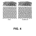
- Ta Ta (Tantalum) as an adhesion promoting material
- Figure 4 displays a fully equilibrated structure upon 4 ps MD simulation. No agglomeration of Cu atoms, other than simple thermal motion, was observed. Placing the same monolayer on multi-layers of Ta results in no agglomeration of Cu atoms.
- the calculated adhesion energy of Cu monolayer on the Ta monolayer is 3.84 eV and the calculated adhesion energy of Ta monolayer on TaN(111) is 7.72 eV, significantly larger than the adhesion energy of Cu monolayer on TaN(111).
- the results suggest that Cu monolayer will not agglomerate on the Ta adhesion promoting layer.
- Figure 5 displays a fully equilibrated structure upon 4 ps MD simulation. No agglomeration of Cu atoms, other than simple thermal motion, was observed. Placing the same monolayer on multi-layers of Cr results in no agglomeration of Cu atoms.
- the calculated adhesion energy of Cu monolayer on the Cr monolayer is 3.52 eV and the calculated adhesion energy of Ta monolayer on TaN(111) is 5.10 eV, significantly larger than the adhesion energy of Cu monolayer on TaN(111). The results suggest that Cu monolayer will not agglomerate on the Cr adhesion promoting layer.
- Figure 6 displays equilibrated structures upon 4 ps MD simulation.
- Figure 6(a) displays a fully equilibrium structure of CrV adhesion promoting layer on TaN(111) surface with top view and side view.
- Figure 6(b) displays a fully equilibrium structure of Cu monolayer on the CrV adhesion promoting layer on TaN(111) surface with top view and side view.
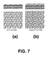
- Figure 7 displays equilibrated structures upon 4 ps MD simulation.
- Figure 7(a) displays the equilibrium structure of CrTi adhesion promoting layer on TaN(111) surface with top view and side view.
- Figure 7(b) displays the equilibrium structure of Cu monolayer on the CrTi adhesion promoting layer on TaN(111) surface with top view and side view.
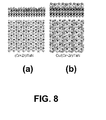
- Figure 8 displays equilibrated structures upon 4 ps MD simulation.
- Figure 8(a) displays the equilibrium structure of CrZr adhesion promoting layer on TaN(111) surface with top view and side view.
- Figure 8(b) displays the equilibrium structure of Cu monolayer on the CrZr adhesion promoting layer on TaN(111) surface with top view and side view.
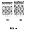
- Figure 9 displays equilibrated structures upon 4 ps MD simulation.
- Figure 9(a) displays the equilibrium structure of CrNb adhesion promoting layer on TaN(111) surface with top view and side view.
- Figure 9(b) displays the equilibrium structure of Cu monolayer on the CrNb adhesion promoting layer on TaN(111) surface with top view and side view.
- the inventors have identified factors responsible for providing good adhesion of copper layer on various metallic surfaces and circumstances under which agglomeration of copper film occur.
- the adhesion energy of the adhesion promoting layer on the barrier layer should be higher than the adhesion energy of copper on the barrier layer.
- the adhesion energy of the copper seed layer on the adhesion promoting layer should be higher than the adhesion energy of copper on the barrier layer (otherwise, the copper seed layer would agglomerate on the glue layer);
- the adhesion energy of adhesion promoting layer on the barrier layer should be higher than the adhesion energy of the copper seed layer on the glue layer.
- Chromium containing complexes of a polydentate ⁇ -ketoiminate have been identified as chromium containing precursors to make the chromium alloys used for the adhesion promoting layer.
Abstract
State-of-the-art computational chemistry techniques have been used to identify adhesion promoting layer materials that provide good adhesion of a metal seed layer, e.g. a copper seed layer, to a barrier layer. Factors responsible for providing good adhesion of copper layer on various metallic surfaces and circumstances under which agglomeration of copper film occurs have been identified. Several promising adhesion promoting layer materials based on ruthenium, tantalum, chromium and chromium alloys have been predicted to be able to significantly enhance the adhesion of copper films. Chromium containing complexes of a polydentate β-ketoiminate have been identified as chromium containing precursors to make the alloys with chromium.
Description
- In the fabrication of semiconductor devices, increased density and speed has caused a shift in the metallization system from aluminum (Al) to copper (Cu) to reduce the resistance of the conductor. To reduce the capacitive coupling between adjacent metal lines, materials having low k dielectric constant are used to form dielectric layers between adjacent metal lines. Furthermore, to prevent diffusion of copper containing materials into the surrounding low k dielectric layers, diffusion barrier layers are incorporated between metal layers and dielectric layers.
- However, due to reliability issues of electromigration resistance and void formation, adhesion between copper and the diffusion barrier layer is a major concern. With typical copper diffusion barrier layers now available, copper has less than desirable adhesion to the barrier layers and has a tendency to agglomerate for future technology nodes such as 22 nm and beyond future size.
-
US 6271131 discloses a method of forming a rhodium (Rh) containing layer such as platinum-rhodium (Pt-Rh) alloy as diffusion barrier via chemical vapor deposition. However Pt and Rh are very expensive noble metals which makes it impossible to adopt in the semi-conductor industries. -
US 6331484 describes a titanium-tantalum (Ti-Ta) barrier layer film for use in conjunction with an interconnect film such as Cu. The Ti rich/Ta deficient portion provides good adhesion to the dielectric film and the Ta rich/Ti deficient portion forms a hetero-epitaxial interface with the interconnect film and suppresses the formation of intermetallic compounds. -
US 5942799 discloses a multilayer diffusion barrier comprising a refractory metal such as tungsten (W), titanium (Ti), tantalum (Ta), molybdenum (Mo); and a refractory metal nitride such as WNx, TiN, TaN; and a second sublayer formed from a refractory metal nitride, a refractory metal silicon nitride such as TiSixNy, TaSixNy, WSixNy. -
US 20050070097 discloses a very thin multilayer diffusion barrier for a semiconductor device and fabrication method thereof. The multilayer diffusion barrier is fabricated by forming a very thin, multilayer diffusion barrier composed of even thinner sub-layers, where the sub-layers are only a few atoms thick. -
US 2006001306 reveals a method to enhance thermal stability and reliability by forming a hybrid type nanocomposite diffusion barrier deposited by atomic layer deposition using precursors composing of a Ti precursor and a Ta precursor. -
WO 2006115476 covers the ruthenium alloy as copper diffusion barrier comprising of ruthenium and at least one element from groups IV, V, or VI of the Periodic Table or a combination thereof. -
US 20070264816 discloses a method for forming a metal interconnect to use a Cu-Al alloy layer on the barrier layer. The Cu--Al alloy layer may be formed by sequential ALD or CVD deposition of an aluminum layer and a copper layer followed by an annealing process. Alternately, the Cu--Al alloy layer may be formed in-situ by co-pulsing the aluminum and copper precursors. -
US 20070123043 describes a tin and nickel-containing copper alloy as diffusion barrier in a copper interconnect. The tin and nickel-containing copper alloy may be formed in a gaseous ambient on the basis of tin hydride and nickel, carbon monoxide in a thermally driven reaction. - Maury, F. and F. Ossola (1992). "Evaluation of Tetra-Alkylchromium Precursors for Organometallic Chemical Vapor-Deposition .2. Unusual Low-Temperature Chromium Carbide Deposition from Cr[C(CH3)3]4." Thin Solid Films 219(1-2): 24-29
- Ossola, F. and F. Maury (1997). "MOCVD route to chromium carbonitride thin films using Cr(NEt2)(4) as single-source precursor: Growth and mechanism." Chemical Vapor Deposition 3(3): 137-143.
- Accordingly, there remains a need for an improved adhesion process, or metallization process, which controls the agglomeration of copper, and improves the adhesion between barrier layers and subsequently deposited metal layers. There is also a need for an adhesion-promoting materials, or glue layer materials, which promote adhesion between barrier layers and subsequently deposited metal layers.
- In the present invention, the state-of-the-art computational chemistry techniques have been used to identify adhesion promoting layer materials that provide good adhesion of metal seed layer to the adhesion promoting layer and the adhesion promoting layer to the barrier layer. Methods of controlling agglomeration and improving adhesion, a semiconductor device structure having controlled agglomeration and improving adhesion, and a chromium precursor for making chromium alloys as the adhesion promoting layer material have also been disclosed.
- According to a first aspect of the present invention, there is provided a method comprising:
- providing a substrate comprising at least one patterned dielectric layer and at least one barrier layer;
- depositing an adhesion promoting layer comprising a chromium alloy on the at least one barrier layer; and
- depositing a metal seed layer on the adhesion promoting layer;
- wherein adhesion energy between the adhesion promoting layer and the barrier layer is higher than adhesion energy between the adhesion promoting layer and the metal seed layer.
- According to a second aspect of the present invention, there is provided a method comprising:
- providing a substrate comprising the at least one barrier layer on the top of at least one patterned dielectric layer;
- depositing an adhesion promoting layer comprising a chromium alloy on the at least one barrier layer, and
- depositing the copper layer on the adhesion promoting layer;
- wherein adhesion energy between the adhesion promoting layer and the barrier layer is higher than adhesion energy between the adhesion promoting layer and the copper layer.
- The method according to the first or second aspect is for producing a semiconductor device. On advantage of such methods is that agglomeration of atoms in a metal seed layer of the semiconductor device is controlled and adhesion between the metal seed layer and a diffusion barrier layer is improved.
- The method according to the first or second aspect is preferably for controlling agglomeration and improving adhesion of a semiconductor device.
- According to a third aspect of the present invention, there is provided a semiconductor device structure comprises:
- at least one patterned dielectric layer and at least one barrier layer covering the at least one patterned dielectric layer;
- an adhesion promoting layer deposited on the at least one barrier layer, said adhesion promoting layer consisting essentially of a chromium alloy; and
- a conductive metal seed layer covering the adhesion promoting layer.
- According to a fourth aspect of the present invention, there is provided a chromium containing complex of a polydentate β-ketoiminate is selected from the group consisting of structure A ,


- each R1 is a branched, e.g. bulky, alkyl group containing 3 to 6 carbon atoms;
- each R2 is selected from the group consisting of hydrogen, alkyl groups having from 1 to 6 carbon atoms, alkoxy groups having from 1 to 6 carbon atoms, cycloaliphatic groups having from 3 to 6 carbon atoms, and aryl groups having from 6 to 10 carbon atoms;
- each R3 is linear or branched, selected from the group consisting of alkyl groups having from 1 to 6 carbon atoms, alkoxy groups having from 1 to 6 carbon atoms, cycloaliphatic groups having from 3 to 6 carbon atoms, and aryl groups having from 6 to 10 carbon atoms;
- each R4 is a linear or branched bridging group selected from the group consisting of alkyl groups having from 1 to 6 carbon atoms, alkoxy groups having from 1 to 6 carbon atoms, cycloaliphatic groups having from 3 to 6 carbon atoms, and aryl groups having from 6 to 10 carbon atoms
- each of R5-6 is linear or branched, individually selected from the group consisting of linear alkyl groups having from 1 to 6 carbon atoms, fluoroalkyl groups having from 1 to 6 carbon atoms, cycloaliphatic groups having from 3 to 10 carbon atoms, aryl groups having from 6 to 10 carbon atoms, and heterocyclic groups containing either oxygen, or nitrogen atoms; and
- L is monodentate donor ligand, e.g. hydroxyl.
- According to a fifth aspect of the present invention, there is provided use of a chromium alloy to control agglomeration in a conductive metal seed layer provided on a barrier layer in a semiconductor device and/or improve adherence of said metal seed layer to said barrier layer.
- Copper adhesion to barrier layers and electromigration resistance are extremely important properties affecting device yield and device lifetimes.
- In the present invention, the state-of-the-art computational chemistry techniques have been used to identify adhesion promoting layer materials that provide good adhesion of metal seed layer to the adhesion promoting layer and the adhesion promoting layer to the barrier layer.
- In accordance with embodiments of the present invention, adhesion promoting layer, or a "glue" layer, is applied directly to a barrier layer to improve the adhesion of the subsequently deposited metal seed layer.
- Suitable barrier layers comprise a material selected from the group consisting of: tantalum (Ta), tantalum-nitride (TaN), tantalum-silicon-nitride (TaSiN), titanium (Ti), titanium-nitride (TiN), and mixtures thereof.
- Suitable metal seed layer is selected from a copper layer, a copper alloy layer, and combinations thereof.
- Several adhesion promoting layer materials based on chromium alloys have been shown to be able to significantly enhance the adhesion of the copper seed layer. The adhesion promoting layer, or a "glue" layer, comprises a chromium alloy having a formulation of CrxMy, where M is a group 4 to 12 metal, such as, copper (Cu), silver (Ag), ruthenium (Ru), vanadium (V), tantalum (Ta), titanium (Ti), zirconium ( Zr) and niobium (Nb), x is the atomic weight percentage of Cr, y is the atomic weight percentage of M, and x+y =100%.
- Suitable chromium alloys including chromium and about 10 % to about 90% atomic weight percentage of an alloying element. As examples, the chromium alloys include chromium-copper (CrxCuy), chromium-silver (CrxAgy), chromium-ruthenium (CrxRuy), chromium-vanadium (CrxVy), chromium-tantalum (CrxTay), chromium-titanium (CrxTiy), chromium-zirconium (CrxZry) and chromium-niobium (CrxNby); where x is in the range of 10% to 90%.
- The adhesion promoting layer may be deposited by a process selected from the group consisting of Atomic Layer Deposition (ALD), Plasma Enhanced Atomic Layer Deposition (PEALD), Chemical Vapor Deposition(CVD), and Plasma Enhanced Chemical Vapor Deposition(PECVD), Low Pressure Chemical Vapor Deposition(LPCVD), Sub Atmospheric Chemical Vapor Deposition(SACVD), UV assisted Chemical Vapor Deposition, Filament assisted Chemical Vapor Deposition (FACVD), and Atmospheric Pressure Chemical Vapor Deposition (APCVD ).
- Suitable chromium containing precursors for depositing the chromium alloys are chromium containing complexes of a polydentate β-ketoiminate represented by the following structures A and B:


- each R1 is a branched, e.g. bulky, alkyl group containing 3 to 6 carbon atoms;
- each R2 is selected from the group consisting of hydrogen, alkyl groups having from 1 to 6 carbon atoms, alkoxy groups having from 1 to 6 carbon atoms, cycloaliphatic groups having from 3 to 6 carbon atoms, and aryl groups having from 6 to 10 carbon atoms;
- each R3 is linear or branched, selected from the group consisting of alkyl groups having from 1 to 6 carbon atoms, alkoxy groups having from 1 to 6 carbon atoms, cycloaliphatic groups having from 3 to 6 carbon atoms, and aryl groups having from 6 to 10 carbon atoms;
- each R4 is a linear or branched bridging group selected from the group consisting of alkyl groups having from 1 to 6 carbon atoms, alkoxy groups having from 1 to 6 carbon atoms, cycloaliphatic groups having from 3 to 6 carbon atoms, and aryl groups having from 6 to 10 carbon atoms;
- each of R5-6 is linear or branched, individually selected from the group consisting of linear alkyl groups having from 1 to 6 carbon atoms, fluoroalkyl groups having from 1 to 6 carbon atoms, cycloaliphatic groups having from 3 to 10 carbon atoms, aryl groups having from 6 to 10 carbon atoms, and heterocyclic groups containing either oxygen, or nitrogen atoms; and
- L is monodentate donor ligand, e.g. hydroxyl.
- Additional objects, advantages, and novel features of this invention will become apparent to those skilled in the art upon examination of the following embodiments thereof, which are not intended to be limiting.
- Examples of the invention will now be described with reference to the following figures:
-
Figure 1 Structure of tantalum-nitride TaN(111) surface: (a) side view; (b) top view; -
Figure 2 Snapshot of the molecular dynamics ("MD") trajectory; -
Figure 3(a) Copper (Cu) monolayer on top of a ruthenium (Ru) monolayer commensurate to the TaN(111) substrate; -
Figure 3(b) initial and equilibrium structures of a Cu monolayer on Ru slab; -
Figure 4 Cu monolayer on top of a tantalum (Ta) monolayer commensurate to the TaN(111) substrate; -
Figure 5 Cu monolayer on top of a chromium (Cr) monolayer commensurate to the TaN(111) substrate; -
Figure 6(a) The equilibrium structure of Chromium binary with Vanadium (CrV) adhesion promoting layer on TaN(111) surface with top view and side view; -
Figure 6(b) The equilibrium structure of Cu monolayer on the CrV adhesion promoting layer on TaN(111) surface with top view and side view; -
Figure 7(a) The equilibrium structure of Chromium binary with Titanium (CrTi) adhesion promoting layer on TaN(111) surface with top view and side view; -
Figure 7(b) The equilibrium structure of Cu monolayer on the CrTi adhesion promoting layer on TaN(111) surface with top view and side view; -
Figure 8(a) The equilibrium structure of Chromium binary with Zirconium (CrZr) adhesion promoting layer on TaN(111) surface with top view and side view; -
Figure 8(b) The equilibrium structure of Cu monolayer on the CrZr adhesion promoting layer on TaN(111) surface with top view and side view; -
Figure 9(a) The equilibrium structure of Chromium binary with Niobium (CrNb) adhesion promoting layer on TaN(111) surface with top view and side view; -
Figure 9(b) The equilibrium structure of Cu monolayer on the CrNb adhesion promoting layer on TaN(111) surface with top view and side view; and -
Figure 10 Crystal structure of bis(2,2-dimethyl-5-(dimethylaminoethyl-imino)-3-hexanonato-N,O,N')(hydroxyl)chromium. - The TaN(111) surface is described with a slab model containing four alternating layers with Ta (tantalum) and N (nitrogen) with N on top (
Figure 1 ). The selected unit cell contains 32 Ta and 32 N atoms and the surface cell parameters were fully optimized (a=12.416Å, b=10.7533Å, alpha=90°). In between slabs there is an approximately 24 Å vacuum space to prevent effective interaction between slabs. The bottom two layers are kept fixed and the top two layers as well as the Cu adatoms are fully relaxed. - Density functional theory (DFT) calculations under the generalized gradient approximation were performed using the exchange-correlation functional proposed by Perdew-Wang (Perdew, J. P. and Wang, Y.; Phys. Rev. B; 1992, 45, 13244). The projector augmented wave ("PAW") pseudopotentials are used to represent the core electrons, while the valence orbitals are described by a plane wave basis set with 400 electon volts ("eV") energy cut-off, which is sufficient to produce well-converged results. The electronically open-shell system was treated with a spin polarization scheme. The Brillouin zone integration was performed using the Monkhorst and Pack scheme (Monkhorst, H. J. and Pack, J. D.; Phys Rev. B; 1976, 13, 5188) with 2×2×1 k-points. Calculations with higher k-points (4×4×2) were also performed for dimer formation on the TaN(111) surface and the results were found to be virtually identical to those obtained with 2×2×1 k-points.
- All structures were first optimized using the conjugate gradient algorithm (Numerical Recipes in C; W. H. Press, S. A. Teukolsky, W. T. Vetterling and B. P. Falnnery; Cambridge University Press; New York, 1992) and the computational accuracy was tested by calculating the cohesive energy of bulk copper. The calculated cohesive energy is 0.05 eV higher than the experimental value of 3.49 eV, suggesting that the method used in the present study is very accurate.
- The inventors subsequently performed ab initio molecular dynamics ("MD") simulations for duration of 3.5 picoseconds ("ps") with a time step of 1 femtosecond ("fs") at 500 K to study the dynamic behavior of a Cu monolayer on the barrier surface in a canonical ensemble using the Nose thermostat for temperature control. All calculations were carried out using the VASP, or the Vienna Ab-initio simulation package.
- Ab initio molecular dynamics simulation (MD) was performed on the fully equilibrated TaN(111) surface with a Cu monolayer at 500 K, which is in a typical atomic layer deposition ("ALD") temperature range.
-
Figure 2 displays several selected snapshots of the MD trajectory. - Initially, the Cu monolayer is well aligned and commensurate with the substrate. Cu atoms are then quickly disassembled and move away from their equilibrium positions through surface diffusion upon MD run. At t=1 ps, some of the Cu atoms start moving upward to grow 3-dimensionally. At t=3 ps, the Cu atoms are aggregated together, forming surface islands, and the perfectly ordered monolayer structure becomes significantly disordered. Further MD runs prompt Cu atoms to move continuously, forming surface islands of various shapes, but no wetting of copper clusters on the surface was observed.
- The calculated adhesion energy of Cu monolayer on TaN(111) is 2.65 eV.
- Ab initio molecular dynamics simulation was performed on the fully equilibrated surface with a Cu monolayer on top of a monolayer of Ru commensurate with TaN(111) surface at 500 K.
-
Figure 3(a) displays a fully equilibrated structure upon 4 ps MD simulation. No agglomeration of Cu atoms, other than simple thermal motion, was observed. Placing the same monolayer on several layers of Ru, as shown inFig. 3(b) , results in no agglomeration of Cu atoms. - The calculated adhesion energy of Cu monolayer on the Ru monolayer is 3.50 eV and the calculated adhesion energy of Ru monolayer on TaN(111) is 5.01 eV, significantly larger than the adhesion energy of Cu monolayer on TaN(111). The results suggest that Cu monolayer will not agglomerate on the Ru adhesion promoting layer.
- Ab initio molecular dynamics simulation was performed on the fully equilibrated surface with a Cu monolayer on top of a monolayer of Ta commensurate with TaN(111) surface at 500 K.
-
Figure 4 displays a fully equilibrated structure upon 4 ps MD simulation. No agglomeration of Cu atoms, other than simple thermal motion, was observed. Placing the same monolayer on multi-layers of Ta results in no agglomeration of Cu atoms. - The calculated adhesion energy of Cu monolayer on the Ta monolayer is 3.84 eV and the calculated adhesion energy of Ta monolayer on TaN(111) is 7.72 eV, significantly larger than the adhesion energy of Cu monolayer on TaN(111). The results suggest that Cu monolayer will not agglomerate on the Ta adhesion promoting layer.
- Ab initio molecular dynamics simulation was performed on the fully equilibrated surface with a Cu monolayer on top of a monolayer of Cr commensurate with TaN(111) surface at 500 K.
-
Figure 5 displays a fully equilibrated structure upon 4 ps MD simulation. No agglomeration of Cu atoms, other than simple thermal motion, was observed. Placing the same monolayer on multi-layers of Cr results in no agglomeration of Cu atoms. The calculated adhesion energy of Cu monolayer on the Cr monolayer is 3.52 eV and the calculated adhesion energy of Ta monolayer on TaN(111) is 5.10 eV, significantly larger than the adhesion energy of Cu monolayer on TaN(111). The results suggest that Cu monolayer will not agglomerate on the Cr adhesion promoting layer. - Ab initio molecular dynamics simulation was performed on the fully equilibrated surface with a Cu monolayer on top of a monolayer of CrxVy alloy with x:y = 1:1 commensurate with TaN(111) surface at 500 K.
-
Figure 6 displays equilibrated structures upon 4 ps MD simulation.Figure 6(a) displays a fully equilibrium structure of CrV adhesion promoting layer on TaN(111) surface with top view and side view.Figure 6(b) displays a fully equilibrium structure of Cu monolayer on the CrV adhesion promoting layer on TaN(111) surface with top view and side view. - No agglomeration of Cu atoms, other than simple thermal motion, was observed. The calculated adhesion energy of Cu monolayer on the CrV alloy monolayer is 3.65 eV and the calculated adhesion energy of CrV monolayer on TaN(111) is 5.03 eV, significantly larger than the adhesion energy of Cu monolayer on TaN(111). The results suggest that Cu monolayer will not agglomerate on the CrV adhesion promoting layer.
- Ab initio molecular dynamics simulation was performed on the fully equilibrated surface with a Cu monolayer on top of a monolayer of CrxTiy alloy with x:y = 1:1 commensurate with TaN(111) surface at 500 K.
-
Figure 7 displays equilibrated structures upon 4 ps MD simulation.Figure 7(a) displays the equilibrium structure of CrTi adhesion promoting layer on TaN(111) surface with top view and side view.Figure 7(b) displays the equilibrium structure of Cu monolayer on the CrTi adhesion promoting layer on TaN(111) surface with top view and side view. - No agglomeration of Cu atoms, other than simple thermal motion, was observed. The calculated adhesion energy of Cu monolayer on the CrTi alloy monolayer is 3.67 eV and the calculated adhesion energy of CrTi monolayer on TaN(111) is 5.51 eV, significantly larger than the adhesion energy of Cu monolayer on TaN(111). The results suggest that Cu monolayer will not agglomerate on the CrTi adhesion promoting layer.
- Ab initio molecular dynamics simulation was performed on the fully equilibrated surface with a Cu monolayer on top of a monolayer of CrxZry alloy with x:y = 1:1 commensurate with TaN(111) surface at 500 K.
-
Figure 8 displays equilibrated structures upon 4 ps MD simulation.Figure 8(a) displays the equilibrium structure of CrZr adhesion promoting layer on TaN(111) surface with top view and side view.Figure 8(b) displays the equilibrium structure of Cu monolayer on the CrZr adhesion promoting layer on TaN(111) surface with top view and side view. - No agglomeration of Cu atoms, other than simple thermal motion, was observed. The calculated adhesion energy of Cu monolayer on the CrZr alloy monolayer is 3.75 eV and the calculated adhesion energy of CrZr monolayer on TaN(111) is 6.09 eV, significantly larger than the adhesion energy of Cu monolayer on TaN(111). The results suggest that Cu monolayer will not agglomerate on the CrZr adhesion promoting layer.
- Ab initio molecular dynamics simulation was performed on the fully equilibrated surface with a Cu monolayer on top of a monolayer of CrxNby alloy with x:y = 1:1 commensurate with TaN(111) surface at 500 K.
-
Figure 9 displays equilibrated structures upon 4 ps MD simulation.Figure 9(a) displays the equilibrium structure of CrNb adhesion promoting layer on TaN(111) surface with top view and side view.Figure 9(b) displays the equilibrium structure of Cu monolayer on the CrNb adhesion promoting layer on TaN(111) surface with top view and side view. - No agglomeration of Cu atoms, other than simple thermal motion, was observed. The calculated adhesion energy of Cu monolayer on the CrNb alloy monolayer is 3.77 eV and the calculated adhesion energy of CrNb monolayer on TaN(111) is 5.64 eV, significantly larger than the adhesion energy of Cu monolayer on TaN(111). The results suggest that Cu monolayer will not agglomerate on the CrNb adhesion promoting.
- To a slushy solution of 3.45 (16.27 mmol) 2,2-dimethyl-5-(dimethylamine-ethylamine)-3-hexanone in 25 mL hexanes at -40°C was added 6.51 mL (16.27 mmol) 2.5M n-BuLi in hexanes drop wise. Warmed yellow-green solution to room temperature and left to stir for 30 minutes. Evaporated off hexanes under vacuum and residual was taken up in 25 mL THF. This solution was added to a suspension of 1.00 g (8.14 mmol) CrCl2 in 10 mL THF at room temperature via canula. Heated to 60°C for 16 hours. Evaporated off volatiles under vacuum to a dark brown oil that was taken up in hot hexanes and filtered. Isolated 2.12g of crude product that was sublimed at 100°C under 90 mTorr (12 Pa) vacuum over a period of 16 hours. Needle-like crystals were grown from pentane from sublimed material. 55% crude yield.
- Crystal structure of bis(2,2-dimethyl-5-(dimethylaminoethyl-imino)-3-hexanonato-N,O,N')(hydroxyl)chromium is shown in
figure 10 . - In summary, several adhesion promoting layer materials based on chromium alloys have been identified to be able to significantly enhance the adhesion of copper films. Table I summarizes the adhesion energy between the barrier layer TaN(111) and the adhesion promoting layer (ΔEAB), and the adhesion energy between the copper seed layer and the adhesion promoting layer (ΔECuA) (unit: eV).
Table 1. The calculated Adhesion Energy (eV) TaN(111) Cu Ru Ta Cr CrTi CrNb CrZr ΔEAB 2.65 5.01 7.72 5.10 5.51 5.64 6.09 ΔECuA 3.50 3.84 3.52 3.67 3.77 3.75 - The inventors have identified factors responsible for providing good adhesion of copper layer on various metallic surfaces and circumstances under which agglomeration of copper film occur.
- To stabilize the adhesion promoting layer and prevent the agglomeration, the adhesion energy of the adhesion promoting layer on the barrier layer should be higher than the adhesion energy of copper on the barrier layer.
- To stabilize the copper film and prevent the agglomeration, the adhesion energy of the copper seed layer on the adhesion promoting layer should be higher than the adhesion energy of copper on the barrier layer (otherwise, the copper seed layer would agglomerate on the glue layer);
- To prevent diffusion of adhesion promoting layer atoms into the copper layer, the adhesion energy of adhesion promoting layer on the barrier layer should be higher than the adhesion energy of the copper seed layer on the glue layer.
- Chromium containing complexes of a polydentate β-ketoiminate have been identified as chromium containing precursors to make the chromium alloys used for the adhesion promoting layer.
- The embodiments of this invention listed above, including the working example, are exemplary of numerous embodiments that may be made of this invention. It is contemplated that numerous other configurations of the process may be used, and the materials used in the process may be elected from numerous materials other than those specifically disclosed.
Claims (15)
- A method for producing a semiconductor device, said method comprising:providing a substrate comprising at least one patterned dielectric layer and at least one barrier layer;depositing an adhesion promoting layer comprising a chromium alloy on the at least one barrier layer; anddepositing a metal seed layer on the adhesion promoting layer;wherein adhesion energy between the adhesion promoting layer and the barrier layer is higher than adhesion energy between the adhesion promoting layer and the metal seed layer.
- A method as claimed in Claim 1 wherein the adhesion promotion layer consists essentially of said chromium alloy.
- A method as claimed in Claim 1 or Claim 2, wherein the chromium alloy has a formulation of CrxMy, wherein M is a metal selected from Group 4 to Group 12 of the periodic table, x is the atomic weight percentage of Cr, y is the atomic weight percentage of M, and x+y =100%.
- A method as claimed in Claim 3 wherein M is selected from the group consisting of copper (Cu), silver (Ag), ruthenium (Ru), vanadium (V), tantalum (Ta), titanium (Ti), zirconium (Zr) and niobium (Nb).
- A method as claimed in any of the preceding claims, wherein the chromium alloy is selected from the group consisting of chromium-copper (CrxCuy), chromium-silver (CrxAgy), chromium-ruthenium (CrxRuy), chromium-vanadium (CrxVy), chromium-tantalum(CrxTay), chromium-titanium (CrxTiy), chromium-zirconium (CrxZry) and chromium-niobium (CrxNby); and wherein x is in the range of 10% to 90%.
- A method as claimed in any of the preceding claims, wherein the chromium alloy is deposited from a chromium containing precursor having complexes of a polydentate β-ketoiminate selected from the group consisting of structure A;

 each R1 is a branched alkyl group containing 3 to 6 carbon atoms;each R2 is selected from the group consisting of hydrogen, alkyl groups having from 1 to 6 carbon atoms, alkoxy groups having from 1 to 6 carbon atoms, cycloaliphatic groups having from 3 to 6 carbon atoms, and aryl groups having from 6 to 10 carbon atoms;each R3 is linear or branched, selected from the group consisting of alkyl groups having from 1 to 6 carbon atoms, alkoxy groups having from 1 to 6 carbon atoms, cycloaliphatic groups having from 3 to 6 carbon atoms, and aryl groups having from 6 to 10 carbon atoms;each R4 is a linear or branched bridging group selected from the group consisting of alkyl groups having from 1 to 6 carbon atoms, alkoxy groups having from 1 to 6 carbon atoms, cycloaliphatic groups having from 3 to 6 carbon atoms, and aryl groups having from 6 to 10 carbon atoms;each of R5-6 is linear or branched, individually selected from the group consisting of linear alkyl groups having from 1 to 6 carbon atoms, fluoroalkyl groups having from 1 to 6 carbon atoms, cycloaliphatic groups having from 3 to 10 carbon atoms, aryl groups having from 6 to 10 carbon atoms, and heterocyclic groups containing either oxygen, or nitrogen atoms; andL is monodentate donor ligand.
 - A method as claimed in any of the preceding claims, wherein the barrier layer comprises a material selected from the group consisting of: tantalum (Ta), tantalum-nitride (TaN), tantalum-silicon-nitride (TaSiN), titanium (Ti), titanium-nitride (TiN), and mixtures thereof.
- A method as claimed in any of the preceding claims, wherein the metal seed layer is selected from the group consisting of a copper layer, a copper alloy layer, and combinations thereof.
- A method as claimed in any of the preceding claims, wherein the adhesion promoting layer is deposed by a process selected from the group consisting of Atomic Layer Deposition (ALD), Plasma Enhanced Atomic Layer Deposition (PEALD), Chemical Vapor Deposition(CVD), and Plasma Enhanced Chemical Vapor Deposition(PECVD), Low Pressure Chemical Vapor Deposition(LPCVD), Sub Atmospheric Chemical Vapor Deposition(SACVD), UV assisted Chemical Vapor Deposition, Filament assisted Chemical Vapor Deposition (FACVD), and Atmospheric Pressure Chemical Vapor Deposition (APCVD ).
- A method as claimed in any of the preceding claims, wherein at least one barrier layer is provided on the top of at least one patterned dielectric layer; an adhesion promoting layer comprising a chromium alloy is deposited on the at least one barrier layer, and a copper layer is deposited on the adhesion promoting layer.
- A semiconductor device structure comprising:at least one patterned dielectric layer and at least one barrier layer covering the at least one patterned dielectric layer;an adhesion promoting layer deposited on the at least one barrier layer, said adhesion promoting layer consisting essentially of a chromium alloy; anda conductive metal seed layer covering the adhesion promoting layer.
- A semiconductor device structure as claimed in Claim 11 wherein the structure is as defined in any of Claims 2 to 10.
- A chromium containing complex of a polydentate β-ketoiminate selected from the group consisting of structure A ,

 each R1 is a branched alkyl group containing 3 to 6 carbon atoms;each R2 is selected from the group consisting of hydrogen, alkyl groups having from 1 to 6 carbon atoms, alkoxy groups having from 1 to 6 carbon atoms, cycloaliphatic groups having from 3 to 6 carbon atoms, and aryl groups having from 6 to 10 carbon atoms;each R3 is linear or branched, selected from the group consisting of alkyl groups having from 1 to 6 carbon atoms, alkoxy groups having from 1 to 6 carbon atoms, cycloaliphatic groups having from 3 to 6 carbon atoms, and aryl groups having from 6 to 10 carbon atoms;each R4 is a linear or branched bridging group selected from the group consisting of alkyl groups having from 1 to 6 carbon atoms, alkoxy groups having from 1 to 6 carbon atoms, cycloaliphatic groups having from 3 to 6 carbon atoms, and aryl groups having from 6 to 10 carbon atoms;each of R5-6 is linear or branched, individually selected from the group consisting of linear alkyl groups having from 1 to 6 carbon atoms, fluoroalkyl groups having from 1 to 6 carbon atoms, cycloaliphatic groups having from 3 to 10 carbon atoms, aryl groups having from 6 to 10 carbon atoms, and heterocyclic groups containing either oxygen, or nitrogen atoms;andL is monodentate donor ligand.
 - Use of a chromium alloy to control agglomeration in a conductive metal seed layer provided on a barrier layer in a semiconductor device and/or improve adherence of said metal seed layer to said barrier layer.
- Use as claimed in Claim 14 wherein the chromium alloy is as defined in any of Claim 3 to 5.
Applications Claiming Priority (1)
| Application Number | Priority Date | Filing Date | Title |
|---|---|---|---|
| US12/192,603 US7919409B2 (en) | 2008-08-15 | 2008-08-15 | Materials for adhesion enhancement of copper film on diffusion barriers |
Publications (1)
| Publication Number | Publication Date |
|---|---|
| EP2154717A2 true EP2154717A2 (en) | 2010-02-17 |
Family
ID=41319973
Family Applications (1)
| Application Number | Title | Priority Date | Filing Date |
|---|---|---|---|
| EP09167949A Withdrawn EP2154717A2 (en) | 2008-08-15 | 2009-08-14 | Materials for adhesion enhancement of copper film on diffusion barriers |
Country Status (6)
| Country | Link |
|---|---|
| US (1) | US7919409B2 (en) |
| EP (1) | EP2154717A2 (en) |
| JP (1) | JP2010062555A (en) |
| KR (1) | KR20100021379A (en) |
| CN (1) | CN101673706A (en) |
| TW (1) | TW201007844A (en) |
Cited By (1)
| Publication number | Priority date | Publication date | Assignee | Title |
|---|---|---|---|---|
| US20140377948A1 (en) * | 2006-12-19 | 2014-12-25 | Spansion Llc | Method of depositing copper using physical vapor deposition |
Families Citing this family (2)
| Publication number | Priority date | Publication date | Assignee | Title |
|---|---|---|---|---|
| US20090237209A1 (en) * | 2008-03-20 | 2009-09-24 | Brian William Seal | Communicating keychain |
| KR100973277B1 (en) * | 2008-08-29 | 2010-07-30 | 주식회사 하이닉스반도체 | Metal wiring of semiconductor device and method for forming the same |
Citations (8)
| Publication number | Priority date | Publication date | Assignee | Title |
|---|---|---|---|---|
| US5942799A (en) | 1997-11-20 | 1999-08-24 | Novellus Systems, Inc. | Multilayer diffusion barriers |
| US6271131B1 (en) | 1998-08-26 | 2001-08-07 | Micron Technology, Inc. | Methods for forming rhodium-containing layers such as platinum-rhodium barrier layers |
| US6331484B1 (en) | 1999-03-29 | 2001-12-18 | Lucent Technologies, Inc. | Titanium-tantalum barrier layer film and method for forming the same |
| US20050070097A1 (en) | 2003-09-29 | 2005-03-31 | International Business Machines Corporation | Atomic laminates for diffusion barrier applications |
| US20060001306A1 (en) | 2004-07-02 | 2006-01-05 | C. Rob. Hammerstein Gmbh & Co. Kg | Automotive vehicle seat with a lengthwise adjustment device, a seat carrier and rear rockers |
| WO2006115476A2 (en) | 2005-04-21 | 2006-11-02 | Honeywell International Inc. | Ruthenium-based materials and ruthenium alloys |
| US20070123043A1 (en) | 2005-11-30 | 2007-05-31 | Christof Streck | A semiconductor device comprising a copper alloy as a barrier layer in a copper metallization layer |
| US20070264816A1 (en) | 2006-05-12 | 2007-11-15 | Lavoie Adrien R | Copper alloy layer for integrated circuit interconnects |
Family Cites Families (29)
| Publication number | Priority date | Publication date | Assignee | Title |
|---|---|---|---|---|
| US5668054A (en) | 1996-01-11 | 1997-09-16 | United Microelectronics Corporation | Process for fabricating tantalum nitride diffusion barrier for copper matallization |
| US6153519A (en) | 1997-03-31 | 2000-11-28 | Motorola, Inc. | Method of forming a barrier layer |
| US6287965B1 (en) | 1997-07-28 | 2001-09-11 | Samsung Electronics Co, Ltd. | Method of forming metal layer using atomic layer deposition and semiconductor device having the metal layer as barrier metal layer or upper or lower electrode of capacitor |
| SG70654A1 (en) * | 1997-09-30 | 2000-02-22 | Ibm | Copper stud structure with refractory metal liner |
| US6140231A (en) | 1999-02-12 | 2000-10-31 | Taiwan Semiconductor Manufacturing Company | Robust diffusion barrier for Cu metallization |
| US6627542B1 (en) | 1999-07-12 | 2003-09-30 | Applied Materials, Inc. | Continuous, non-agglomerated adhesion of a seed layer to a barrier layer |
| AU1208201A (en) | 1999-10-15 | 2001-04-30 | Asm America, Inc. | Method for depositing nanolaminate thin films on sensitive surfaces |
| US6596888B2 (en) | 2000-05-15 | 2003-07-22 | University Of Florida | MOCVD of WNx thin films using imido precursors |
| US6194310B1 (en) | 2000-06-01 | 2001-02-27 | Sharp Laboratories Of America, Inc. | Method of forming amorphous conducting diffusion barriers |
| US6797608B1 (en) | 2000-06-05 | 2004-09-28 | Taiwan Semiconductor Manufacturing Company, Ltd. | Method of forming multilayer diffusion barrier for copper interconnections |
| US6539625B2 (en) * | 2001-01-11 | 2003-04-01 | International Business Machines Corporation | Chromium adhesion layer for copper vias in low-k technology |
| US6607976B2 (en) | 2001-09-25 | 2003-08-19 | Applied Materials, Inc. | Copper interconnect barrier layer structure and formation method |
| JP2003298203A (en) * | 2002-03-29 | 2003-10-17 | Nippon Zeon Co Ltd | Printed wiring board and manufacturing method thereof |
| JP4228270B2 (en) * | 2002-07-02 | 2009-02-25 | 富士通株式会社 | Method for forming conductor pattern and mounting circuit board |
| US20050274621A1 (en) | 2004-06-10 | 2005-12-15 | Zhi-Wen Sun | Method of barrier layer surface treatment to enable direct copper plating on barrier metal |
| US6989321B2 (en) | 2003-09-30 | 2006-01-24 | Tokyo Electron Limited | Low-pressure deposition of metal layers from metal-carbonyl precursors |
| US20050167837A1 (en) | 2004-01-21 | 2005-08-04 | International Business Machines Corporation | Device with area array pads for test probing |
| KR101050863B1 (en) | 2004-06-30 | 2011-07-20 | 매그나칩 반도체 유한회사 | Method of forming diffusion barrier in semiconductor device |
| JP4322189B2 (en) * | 2004-09-02 | 2009-08-26 | 株式会社ルネサステクノロジ | Semiconductor device |
| US7223695B2 (en) | 2004-09-30 | 2007-05-29 | Intel Corporation | Methods to deposit metal alloy barrier layers |
| US7034169B1 (en) * | 2004-12-30 | 2006-04-25 | Air Products And Chemicals, Inc. | Volatile metal β-ketoiminate complexes |
| US7205422B2 (en) * | 2004-12-30 | 2007-04-17 | Air Products And Chemicals, Inc. | Volatile metal β-ketoiminate and metal β-diiminate complexes |
| FR2883287A1 (en) | 2005-03-16 | 2006-09-22 | Air Liquide | Preparing organometallic precursor molecules comprises introducing reagents in reactor, reacting to obtain solid-liquid phase mixture, filtering to recover liquid phase and removing solvents present in liquid phase by distillation |
| US7220671B2 (en) | 2005-03-31 | 2007-05-22 | Intel Corporation | Organometallic precursors for the chemical phase deposition of metal films in interconnect applications |
| JP2007103834A (en) * | 2005-10-07 | 2007-04-19 | Taiyo Yuden Co Ltd | Semiconductor device and method for manufacturing the same |
| US7723225B2 (en) * | 2006-02-07 | 2010-05-25 | Stats Chippac Ltd. | Solder bump confinement system for an integrated circuit package |
| US7947814B2 (en) * | 2006-04-25 | 2011-05-24 | Air Products And Chemicals, Inc. | Metal complexes of polydentate beta-ketoiminates |
| US8168811B2 (en) * | 2008-07-22 | 2012-05-01 | Advanced Technology Materials, Inc. | Precursors for CVD/ALD of metal-containing films |
| CN101838210B (en) * | 2009-03-11 | 2014-05-28 | 气体产品与化学公司 | Method for preparing metal complexes of polydentate beta-ketoiminates |
-
2008
- 2008-08-15 US US12/192,603 patent/US7919409B2/en not_active Expired - Fee Related
-
2009
- 2009-08-12 TW TW098127186A patent/TW201007844A/en unknown
- 2009-08-14 EP EP09167949A patent/EP2154717A2/en not_active Withdrawn
- 2009-08-14 JP JP2009188053A patent/JP2010062555A/en active Pending
- 2009-08-14 KR KR1020090075179A patent/KR20100021379A/en active IP Right Grant
- 2009-08-14 CN CN200910173396A patent/CN101673706A/en active Pending
Patent Citations (8)
| Publication number | Priority date | Publication date | Assignee | Title |
|---|---|---|---|---|
| US5942799A (en) | 1997-11-20 | 1999-08-24 | Novellus Systems, Inc. | Multilayer diffusion barriers |
| US6271131B1 (en) | 1998-08-26 | 2001-08-07 | Micron Technology, Inc. | Methods for forming rhodium-containing layers such as platinum-rhodium barrier layers |
| US6331484B1 (en) | 1999-03-29 | 2001-12-18 | Lucent Technologies, Inc. | Titanium-tantalum barrier layer film and method for forming the same |
| US20050070097A1 (en) | 2003-09-29 | 2005-03-31 | International Business Machines Corporation | Atomic laminates for diffusion barrier applications |
| US20060001306A1 (en) | 2004-07-02 | 2006-01-05 | C. Rob. Hammerstein Gmbh & Co. Kg | Automotive vehicle seat with a lengthwise adjustment device, a seat carrier and rear rockers |
| WO2006115476A2 (en) | 2005-04-21 | 2006-11-02 | Honeywell International Inc. | Ruthenium-based materials and ruthenium alloys |
| US20070123043A1 (en) | 2005-11-30 | 2007-05-31 | Christof Streck | A semiconductor device comprising a copper alloy as a barrier layer in a copper metallization layer |
| US20070264816A1 (en) | 2006-05-12 | 2007-11-15 | Lavoie Adrien R | Copper alloy layer for integrated circuit interconnects |
Non-Patent Citations (5)
| Title |
|---|
| MAURY, F.; F. OSSOLA: "Evaluation of Tetra-Alkylchromium Precursors for Organometallic Chemical Vapor-Deposition 2. Unusual Low-Temperature Chromium Carbide Deposition from Cr[C(CH3)3]4", THIN SOLID FILMS, vol. 219, no. 1-2, 1992, pages 24 - 29 |
| MONKHORST, H. J.; PACK, J. D., PHYS REV. B, vol. 13, 1976, pages 5188 |
| OSSOLA, F.; F. MAURY: "MOCVD route to chromium carbonitride thin films using Cr(NEt2)(4) as single-source precursor: Growth and mechanism", CHEMICAL VAPOR DEPOSITION, vol. 3, no. 3, 1997, pages 137 - 143 |
| PERDEW, J. P; WANG, Y., PHYS. REV. B, vol. 45, 1992, pages 13244 |
| W. H. PRESS ET AL.: "Numerical Recipes", 1992, CAMBRIDGE UNIVERSITY PRESS |
Cited By (2)
| Publication number | Priority date | Publication date | Assignee | Title |
|---|---|---|---|---|
| US20140377948A1 (en) * | 2006-12-19 | 2014-12-25 | Spansion Llc | Method of depositing copper using physical vapor deposition |
| US9728414B2 (en) | 2006-12-19 | 2017-08-08 | Cypress Semiconductor Corporation | Method of depositing copper using physical vapor deposition |
Also Published As
| Publication number | Publication date |
|---|---|
| US7919409B2 (en) | 2011-04-05 |
| CN101673706A (en) | 2010-03-17 |
| JP2010062555A (en) | 2010-03-18 |
| TW201007844A (en) | 2010-02-16 |
| US20100038785A1 (en) | 2010-02-18 |
| KR20100021379A (en) | 2010-02-24 |
Similar Documents
| Publication | Publication Date | Title |
|---|---|---|
| US11155919B2 (en) | ALD of metal-containing films using cyclopentadienyl compounds | |
| Chang et al. | Structural and thermodynamic factors of suppressed interdiffusion kinetics in multi-component high-entropy materials | |
| Kwon et al. | Atomic layer deposition of ruthenium thin films for copper glue layer | |
| Kalutarage et al. | Low-temperature atomic layer deposition of copper films using borane dimethylamine as the reducing co-reagent | |
| TWI300098B (en) | Method for increasing deposition rates of metal layers from metal-carbonyl precursors | |
| CN101278387B (en) | Amine-free deposition of metal-nitride films | |
| Ma et al. | Uptake of copper acetamidinate ALD precursors on nickel surfaces | |
| KR101067364B1 (en) | Conductive film forming method, thin film transistor, panel with thin film transistor and thin film transistor manufacturing method | |
| JP2008013848A5 (en) | ||
| Bhandari et al. | Chemical vapor deposition of cobalt nitride and its application as an adhesion-enhancing layer for advanced copper interconnects | |
| EP2154717A2 (en) | Materials for adhesion enhancement of copper film on diffusion barriers | |
| US6337148B1 (en) | Copper source reagent compositions, and method of making and using same for microelectronic device structures | |
| WO2005124847A1 (en) | Semiconductor device and manufacturing method thereof | |
| Chen et al. | Interdiffusion reliability and resistivity scaling of intermetallic compounds as advanced interconnect materials | |
| Lee et al. | Atomic layer deposition of Pt thin films using dimethyl (N, N-dimethyl-3-butene-1-amine-N) platinum and O2 reactant | |
| TW440937B (en) | Iridium conductive electrode/barrier structure and method for same | |
| JP6043835B1 (en) | Chemical vapor deposition material comprising heterogeneous binuclear complex and chemical vapor deposition method using the chemical vapor deposition material | |
| Wong et al. | Prospective development in diffusion barrier layers for copper metallization in LSI | |
| EP2253589A1 (en) | Thin film of metal silicon compound and process for producing the thin film of metal silicon compound | |
| Shin et al. | Growth of ultrathin films of amorphous ruthenium− phosphorus alloys using a single source CVD precursor | |
| Sari et al. | Improvement of the Diffusion Barrier Performance of Ru by Incorporating a WN x Thin Film for Direct-Plateable Cu Interconnects | |
| Bhaskaran et al. | Low-Pressure Chemical Vapor Deposition of Cu− Pd Films: Alloy Growth Kinetics | |
| CN101819944A (en) | Method for forming copper contact interconnection structure | |
| JP2010095795A (en) | Ruthenium-containing thin film and method for production thereof | |
| US7834206B2 (en) | Organic-metal precursor material and method of manufacturing metal thin film using the same |
Legal Events
| Date | Code | Title | Description |
|---|---|---|---|
| PUAI | Public reference made under article 153(3) epc to a published international application that has entered the european phase |
Free format text: ORIGINAL CODE: 0009012 |
|
| AK | Designated contracting states |
Kind code of ref document: A2 Designated state(s): AT BE BG CH CY CZ DE DK EE ES FI FR GB GR HR HU IE IS IT LI LT LU LV MC MK MT NL NO PL PT RO SE SI SK SM TR |
|
| AX | Request for extension of the european patent |
Extension state: AL BA RS |
|
| STAA | Information on the status of an ep patent application or granted ep patent |
Free format text: STATUS: THE APPLICATION HAS BEEN WITHDRAWN |
|
| 18W | Application withdrawn |
Effective date: 20111116 |