EP2153475B1 - Light-guide solar panel and method of fabrication thereof - Google Patents
Light-guide solar panel and method of fabrication thereof Download PDFInfo
- Publication number
- EP2153475B1 EP2153475B1 EP08748233.7A EP08748233A EP2153475B1 EP 2153475 B1 EP2153475 B1 EP 2153475B1 EP 08748233 A EP08748233 A EP 08748233A EP 2153475 B1 EP2153475 B1 EP 2153475B1
- Authority
- EP
- European Patent Office
- Prior art keywords
- light
- optical
- stage
- solar panel
- optical waveguide
- Prior art date
- Legal status (The legal status is an assumption and is not a legal conclusion. Google has not performed a legal analysis and makes no representation as to the accuracy of the status listed.)
- Active
Links
- 238000004519 manufacturing process Methods 0.000 title description 9
- 230000003287 optical effect Effects 0.000 claims description 245
- 238000003780 insertion Methods 0.000 claims description 66
- 239000000463 material Substances 0.000 claims description 61
- 238000002347 injection Methods 0.000 claims description 14
- 239000007924 injection Substances 0.000 claims description 14
- 238000005253 cladding Methods 0.000 claims description 11
- 230000037431 insertion Effects 0.000 claims description 10
- 238000011144 upstream manufacturing Methods 0.000 claims description 5
- 239000011810 insulating material Substances 0.000 claims description 2
- 239000010410 layer Substances 0.000 description 53
- 238000000034 method Methods 0.000 description 16
- 238000013459 approach Methods 0.000 description 12
- 229910052782 aluminium Inorganic materials 0.000 description 10
- XAGFODPZIPBFFR-UHFFFAOYSA-N aluminium Chemical compound [Al] XAGFODPZIPBFFR-UHFFFAOYSA-N 0.000 description 10
- 239000012141 concentrate Substances 0.000 description 9
- 239000007789 gas Substances 0.000 description 9
- XLYOFNOQVPJJNP-UHFFFAOYSA-N water Substances O XLYOFNOQVPJJNP-UHFFFAOYSA-N 0.000 description 9
- 238000003306 harvesting Methods 0.000 description 8
- 230000008901 benefit Effects 0.000 description 7
- 229920003229 poly(methyl methacrylate) Polymers 0.000 description 7
- 239000004926 polymethyl methacrylate Substances 0.000 description 7
- 229920001296 polysiloxane Polymers 0.000 description 7
- 230000009977 dual effect Effects 0.000 description 6
- 239000011521 glass Substances 0.000 description 6
- 230000007246 mechanism Effects 0.000 description 6
- 239000000758 substrate Substances 0.000 description 6
- 239000004593 Epoxy Substances 0.000 description 5
- 230000000694 effects Effects 0.000 description 5
- 238000000465 moulding Methods 0.000 description 5
- -1 poly(methyl-methacrylate) Polymers 0.000 description 5
- 230000001902 propagating effect Effects 0.000 description 5
- XKRFYHLGVUSROY-UHFFFAOYSA-N Argon Chemical compound [Ar] XKRFYHLGVUSROY-UHFFFAOYSA-N 0.000 description 4
- 239000000853 adhesive Substances 0.000 description 4
- 230000001070 adhesive effect Effects 0.000 description 4
- 230000005611 electricity Effects 0.000 description 4
- 239000008393 encapsulating agent Substances 0.000 description 4
- 229920000642 polymer Polymers 0.000 description 4
- 230000008569 process Effects 0.000 description 4
- 201000009310 astigmatism Diseases 0.000 description 3
- 230000000295 complement effect Effects 0.000 description 3
- 230000008878 coupling Effects 0.000 description 3
- 238000010168 coupling process Methods 0.000 description 3
- 238000005859 coupling reaction Methods 0.000 description 3
- 238000013461 design Methods 0.000 description 3
- 239000005038 ethylene vinyl acetate Substances 0.000 description 3
- 239000000835 fiber Substances 0.000 description 3
- 238000009434 installation Methods 0.000 description 3
- 239000007788 liquid Substances 0.000 description 3
- RYGMFSIKBFXOCR-UHFFFAOYSA-N Copper Chemical compound [Cu] RYGMFSIKBFXOCR-UHFFFAOYSA-N 0.000 description 2
- 241000950638 Symphysodon discus Species 0.000 description 2
- 238000009825 accumulation Methods 0.000 description 2
- 229910052786 argon Inorganic materials 0.000 description 2
- 230000000712 assembly Effects 0.000 description 2
- 238000000429 assembly Methods 0.000 description 2
- 230000008859 change Effects 0.000 description 2
- 238000000748 compression moulding Methods 0.000 description 2
- 229910052802 copper Inorganic materials 0.000 description 2
- 239000010949 copper Substances 0.000 description 2
- 239000000428 dust Substances 0.000 description 2
- 239000012530 fluid Substances 0.000 description 2
- 238000009432 framing Methods 0.000 description 2
- 238000013007 heat curing Methods 0.000 description 2
- 238000010438 heat treatment Methods 0.000 description 2
- HOQADATXFBOEGG-UHFFFAOYSA-N isofenphos Chemical compound CCOP(=S)(NC(C)C)OC1=CC=CC=C1C(=O)OC(C)C HOQADATXFBOEGG-UHFFFAOYSA-N 0.000 description 2
- 239000002346 layers by function Substances 0.000 description 2
- 238000012552 review Methods 0.000 description 2
- 230000001932 seasonal effect Effects 0.000 description 2
- 238000005476 soldering Methods 0.000 description 2
- 239000000243 solution Substances 0.000 description 2
- 238000001228 spectrum Methods 0.000 description 2
- 239000004812 Fluorinated ethylene propylene Substances 0.000 description 1
- VYPSYNLAJGMNEJ-UHFFFAOYSA-N Silicium dioxide Chemical compound O=[Si]=O VYPSYNLAJGMNEJ-UHFFFAOYSA-N 0.000 description 1
- 238000004026 adhesive bonding Methods 0.000 description 1
- 239000002390 adhesive tape Substances 0.000 description 1
- 230000002411 adverse Effects 0.000 description 1
- 230000004075 alteration Effects 0.000 description 1
- 238000005219 brazing Methods 0.000 description 1
- DQXBYHZEEUGOBF-UHFFFAOYSA-N but-3-enoic acid;ethene Chemical compound C=C.OC(=O)CC=C DQXBYHZEEUGOBF-UHFFFAOYSA-N 0.000 description 1
- 239000011248 coating agent Substances 0.000 description 1
- 238000000576 coating method Methods 0.000 description 1
- 230000001427 coherent effect Effects 0.000 description 1
- 238000009749 continuous casting Methods 0.000 description 1
- 230000008602 contraction Effects 0.000 description 1
- 238000005260 corrosion Methods 0.000 description 1
- 230000007797 corrosion Effects 0.000 description 1
- 238000001723 curing Methods 0.000 description 1
- 230000007423 decrease Effects 0.000 description 1
- 230000003247 decreasing effect Effects 0.000 description 1
- 239000002274 desiccant Substances 0.000 description 1
- 238000010586 diagram Methods 0.000 description 1
- 238000004049 embossing Methods 0.000 description 1
- 125000003700 epoxy group Chemical group 0.000 description 1
- HQQADJVZYDDRJT-UHFFFAOYSA-N ethene;prop-1-ene Chemical group C=C.CC=C HQQADJVZYDDRJT-UHFFFAOYSA-N 0.000 description 1
- 239000000284 extract Substances 0.000 description 1
- 238000001125 extrusion Methods 0.000 description 1
- 239000005350 fused silica glass Substances 0.000 description 1
- 239000003365 glass fiber Substances 0.000 description 1
- 239000008236 heating water Substances 0.000 description 1
- 238000001746 injection moulding Methods 0.000 description 1
- 238000005304 joining Methods 0.000 description 1
- 238000003475 lamination Methods 0.000 description 1
- 229910052751 metal Inorganic materials 0.000 description 1
- 239000002184 metal Substances 0.000 description 1
- 238000012986 modification Methods 0.000 description 1
- 230000004048 modification Effects 0.000 description 1
- 238000012856 packing Methods 0.000 description 1
- 238000000059 patterning Methods 0.000 description 1
- 229920009441 perflouroethylene propylene Polymers 0.000 description 1
- 230000000737 periodic effect Effects 0.000 description 1
- 229920001200 poly(ethylene-vinyl acetate) Polymers 0.000 description 1
- 229920000647 polyepoxide Polymers 0.000 description 1
- 230000000644 propagated effect Effects 0.000 description 1
- 230000009467 reduction Effects 0.000 description 1
- 238000007789 sealing Methods 0.000 description 1
- 229920002379 silicone rubber Polymers 0.000 description 1
- 239000004945 silicone rubber Substances 0.000 description 1
- 229910000679 solder Inorganic materials 0.000 description 1
Images


Classifications
-
- H—ELECTRICITY
- H01—ELECTRIC ELEMENTS
- H01L—SEMICONDUCTOR DEVICES NOT COVERED BY CLASS H10
- H01L31/00—Semiconductor devices sensitive to infrared radiation, light, electromagnetic radiation of shorter wavelength or corpuscular radiation and specially adapted either for the conversion of the energy of such radiation into electrical energy or for the control of electrical energy by such radiation; Processes or apparatus specially adapted for the manufacture or treatment thereof or of parts thereof; Details thereof
- H01L31/04—Semiconductor devices sensitive to infrared radiation, light, electromagnetic radiation of shorter wavelength or corpuscular radiation and specially adapted either for the conversion of the energy of such radiation into electrical energy or for the control of electrical energy by such radiation; Processes or apparatus specially adapted for the manufacture or treatment thereof or of parts thereof; Details thereof adapted as photovoltaic [PV] conversion devices
- H01L31/054—Optical elements directly associated or integrated with the PV cell, e.g. light-reflecting means or light-concentrating means
-
- G—PHYSICS
- G02—OPTICS
- G02B—OPTICAL ELEMENTS, SYSTEMS OR APPARATUS
- G02B19/00—Condensers, e.g. light collectors or similar non-imaging optics
- G02B19/0004—Condensers, e.g. light collectors or similar non-imaging optics characterised by the optical means employed
-
- F—MECHANICAL ENGINEERING; LIGHTING; HEATING; WEAPONS; BLASTING
- F21—LIGHTING
- F21S—NON-PORTABLE LIGHTING DEVICES; SYSTEMS THEREOF; VEHICLE LIGHTING DEVICES SPECIALLY ADAPTED FOR VEHICLE EXTERIORS
- F21S11/00—Non-electric lighting devices or systems using daylight
-
- G—PHYSICS
- G02—OPTICS
- G02B—OPTICAL ELEMENTS, SYSTEMS OR APPARATUS
- G02B19/00—Condensers, e.g. light collectors or similar non-imaging optics
- G02B19/0004—Condensers, e.g. light collectors or similar non-imaging optics characterised by the optical means employed
- G02B19/0019—Condensers, e.g. light collectors or similar non-imaging optics characterised by the optical means employed having reflective surfaces only (e.g. louvre systems, systems with multiple planar reflectors)
-
- G—PHYSICS
- G02—OPTICS
- G02B—OPTICAL ELEMENTS, SYSTEMS OR APPARATUS
- G02B19/00—Condensers, e.g. light collectors or similar non-imaging optics
- G02B19/0004—Condensers, e.g. light collectors or similar non-imaging optics characterised by the optical means employed
- G02B19/0028—Condensers, e.g. light collectors or similar non-imaging optics characterised by the optical means employed refractive and reflective surfaces, e.g. non-imaging catadioptric systems
-
- H—ELECTRICITY
- H01—ELECTRIC ELEMENTS
- H01L—SEMICONDUCTOR DEVICES NOT COVERED BY CLASS H10
- H01L31/00—Semiconductor devices sensitive to infrared radiation, light, electromagnetic radiation of shorter wavelength or corpuscular radiation and specially adapted either for the conversion of the energy of such radiation into electrical energy or for the control of electrical energy by such radiation; Processes or apparatus specially adapted for the manufacture or treatment thereof or of parts thereof; Details thereof
- H01L31/02—Details
- H01L31/0232—Optical elements or arrangements associated with the device
- H01L31/02327—Optical elements or arrangements associated with the device the optical elements being integrated or being directly associated to the device, e.g. back reflectors
-
- H—ELECTRICITY
- H01—ELECTRIC ELEMENTS
- H01L—SEMICONDUCTOR DEVICES NOT COVERED BY CLASS H10
- H01L31/00—Semiconductor devices sensitive to infrared radiation, light, electromagnetic radiation of shorter wavelength or corpuscular radiation and specially adapted either for the conversion of the energy of such radiation into electrical energy or for the control of electrical energy by such radiation; Processes or apparatus specially adapted for the manufacture or treatment thereof or of parts thereof; Details thereof
- H01L31/04—Semiconductor devices sensitive to infrared radiation, light, electromagnetic radiation of shorter wavelength or corpuscular radiation and specially adapted either for the conversion of the energy of such radiation into electrical energy or for the control of electrical energy by such radiation; Processes or apparatus specially adapted for the manufacture or treatment thereof or of parts thereof; Details thereof adapted as photovoltaic [PV] conversion devices
- H01L31/054—Optical elements directly associated or integrated with the PV cell, e.g. light-reflecting means or light-concentrating means
- H01L31/0547—Optical elements directly associated or integrated with the PV cell, e.g. light-reflecting means or light-concentrating means comprising light concentrating means of the reflecting type, e.g. parabolic mirrors, concentrators using total internal reflection
-
- G—PHYSICS
- G02—OPTICS
- G02B—OPTICAL ELEMENTS, SYSTEMS OR APPARATUS
- G02B6/00—Light guides; Structural details of arrangements comprising light guides and other optical elements, e.g. couplings
- G02B6/0001—Light guides; Structural details of arrangements comprising light guides and other optical elements, e.g. couplings specially adapted for lighting devices or systems
- G02B6/0011—Light guides; Structural details of arrangements comprising light guides and other optical elements, e.g. couplings specially adapted for lighting devices or systems the light guides being planar or of plate-like form
- G02B6/0033—Means for improving the coupling-out of light from the light guide
- G02B6/0035—Means for improving the coupling-out of light from the light guide provided on the surface of the light guide or in the bulk of it
- G02B6/0038—Linear indentations or grooves, e.g. arc-shaped grooves or meandering grooves, extending over the full length or width of the light guide
-
- G—PHYSICS
- G02—OPTICS
- G02B—OPTICAL ELEMENTS, SYSTEMS OR APPARATUS
- G02B6/00—Light guides; Structural details of arrangements comprising light guides and other optical elements, e.g. couplings
- G02B6/0001—Light guides; Structural details of arrangements comprising light guides and other optical elements, e.g. couplings specially adapted for lighting devices or systems
- G02B6/0011—Light guides; Structural details of arrangements comprising light guides and other optical elements, e.g. couplings specially adapted for lighting devices or systems the light guides being planar or of plate-like form
- G02B6/0075—Arrangements of multiple light guides
- G02B6/0078—Side-by-side arrangements, e.g. for large area displays
-
- Y—GENERAL TAGGING OF NEW TECHNOLOGICAL DEVELOPMENTS; GENERAL TAGGING OF CROSS-SECTIONAL TECHNOLOGIES SPANNING OVER SEVERAL SECTIONS OF THE IPC; TECHNICAL SUBJECTS COVERED BY FORMER USPC CROSS-REFERENCE ART COLLECTIONS [XRACs] AND DIGESTS
- Y02—TECHNOLOGIES OR APPLICATIONS FOR MITIGATION OR ADAPTATION AGAINST CLIMATE CHANGE
- Y02E—REDUCTION OF GREENHOUSE GAS [GHG] EMISSIONS, RELATED TO ENERGY GENERATION, TRANSMISSION OR DISTRIBUTION
- Y02E10/00—Energy generation through renewable energy sources
- Y02E10/50—Photovoltaic [PV] energy
- Y02E10/52—PV systems with concentrators
-
- Y—GENERAL TAGGING OF NEW TECHNOLOGICAL DEVELOPMENTS; GENERAL TAGGING OF CROSS-SECTIONAL TECHNOLOGIES SPANNING OVER SEVERAL SECTIONS OF THE IPC; TECHNICAL SUBJECTS COVERED BY FORMER USPC CROSS-REFERENCE ART COLLECTIONS [XRACs] AND DIGESTS
- Y10—TECHNICAL SUBJECTS COVERED BY FORMER USPC
- Y10T—TECHNICAL SUBJECTS COVERED BY FORMER US CLASSIFICATION
- Y10T29/00—Metal working
- Y10T29/49—Method of mechanical manufacture
- Y10T29/49826—Assembling or joining
Definitions
- the present invention relates generally to solar panels. More particularly, the present invention relates to light-guiding concentrator solar panels.
- PV cell material is expensive and solutions have been sought to reduce the amount of PV cell material required in solar panels.
- One of these solutions makes use of concentrating optical elements, such as lenses and mirrors, to concentrate sunlight on a smaller surface area occupied by a correspondingly smaller PV cell.
- the concentrating optical elements all have a non-zero focal length, they make for concentrated photovoltaic (CPV) modules that are typically bulkier than their non-concentrating counterparts. This bulkiness is disadvantageous not only in terms of the handling of the CPV modules, but also in terms of material costs. It is possible to obtain less bulky CPV modules while maintaining the same concentration factor by reducing the size of the PV cell; however, dicing PV cells into smaller cells increases the complexity and cost of the modules.
- present CPV modules typically require that the concentrating optical elements be secured in a complex structural enclosure to hold all the elements in place. This invariably adds to the weight and cost of the CPV modules, and makes for either stricter shipping requirements to mitigate risk of breakage of the assembled CPV modules or, requires that the CPV modules be shipped disassembled to their destination, thereby requiring assembly time and effort at the receiving destination.
- Document US 2002/148497 A1 describes a generic concentrating module having a guide tube device with a plurality of entrance faces directed to optical concentrating elements to focus sunlight beams to a plurality of curved guide tubes coupled to a conical trunk portion.
- Document US 3,780,722 A discloses a concentrating solar collector having a plurality of fibre optic boules made of a bundle of glass fibres having an enlarged upper portion to passively concentrate and deliver sunlight to a thermoelectric generator.
- the present invention provides a light-guide solar panel operable in conjunction with a solar energy collector, the light-guide solar panel comprising:
- the solar panel can have the optical elements spaced-apart from each other along substantially parallel lines and the output surface can be substantially non-orthogonal to the input surface.
- the solar panel can have the optical elements spaced-apart from each other along substantially concentric circle arcs, and the output surface can be shaped as a circle arc substantially concentric with the optical elements.
- the solar panel can have the optical elements include at least one of parabolic reflectors, cubic reflectors, hyperbolic reflectors, elliptical reflectors, flat reflectors, and round reflectors.
- the solar panel can have the optical waveguide stage wedge-shaped.
- the solar panel can have the optical waveguide stage at least partially cone-shaped.
- the solar panel has the optical waveguide stage including a first surface off of which the light received from the at least one optical output aperture goes through a first total internal reflection.
- the solar panel as claimed can have at least one of the input surface and the first surface with a cladding layer formed thereon.
- the solar panel as claimed has the optical waveguide section with a plurality of reflector elements formed opposite the first surface, the plurality of reflector elements for receiving totally internally reflected light from the first surface and for reflecting the totally internally reflected light towards the first surface.
- the plurality of reflector elements can include planar reflectors.
- the planar reflectors can be substantially parallel to the first surface.
- Said plurality of reflector elements have total internal reflection surfaces.
- the at least one optical output aperture is located in between adjacent reflector elements.
- the solar panel as claimed is such that substantially no light is coupled from the optical waveguide stage to the light-insertion stage through the at least one optical output aperture.
- the solar panel is such that the optical waveguide stage guides the light towards the output surface through a series of total internal reflections.
- the solar panel is such that the input surface has a light input area and the output surface has a light collecting area, the light collecting area being smaller than the light input area.
- the solar panel can comprise a solar energy collector optically coupled to the output surface.
- the solar energy collector can include at least one of a photovoltaic solar cell and a heat collector.
- the solar panel can further comprise an optical prism for optically coupling the output surface to the solar energy collector.
- the solar panel can be such that the optical waveguide stage has at least one parabolically-shaped interface adjacent the output surface, the at least one parabolically-shaped interface for concentrating the light on the output surface.
- the solar panel can comprise a tapered optical element adjacent the output surface, the tapered optical element for spacing the solar energy collector from the optical waveguide stage and for concentrating the light onto the solar energy collector.
- the tapered optical element can have a refractive index different than that of the optical waveguide stage.
- the solar panel can have the optical waveguide stage include a plurality of waveguides, each waveguide being optically coupled to one of the at least one optical output aperture, each waveguide for receiving the light from a corresponding optical output aperture and for propagating the light along the waveguide in a direction determined at least by the optical elements.
- Each waveguide can have a waveguide output surface, the waveguide stage output surface comprising the waveguide output surface of each waveguide.
- the optical elements can direct the light to propagate in only one direction along each waveguide or in two opposite directions along each waveguide.
- the optical elements can include a volume phase hologram.
- the optical elements can include a plurality of prismatic ridges.
- the solar panel can be such that the light-insertion stage can include a plurality of tapered light channels and the optical waveguide stage can include a plurality of waveguides, at least one of the tapered light channels being optically coupled to at least one waveguide through one of the at least one optical output aperture, each waveguide for guiding the light along the waveguide in a propagation direction determined at least by the optical elements.
- the at least one waveguide can include waveguides of different diameters.
- the optical elements can include at least one of a volume phase hologram and prismatic ridges for imparting the propagation direction to the light.
- the optical elements can further include at least one of parabolic reflectors, cubic reflectors, hyperbolic reflectors, elliptical reflectors, flat reflectors and round reflectors.
- the light-insertion stage is formed in a first slab of optically transmissive material and the optical waveguide stage is formed in a second slab of optically transmissive material.
- the first slab includes the input surface and the optical elements, and has an output profiled surface opposite the input surface.
- the second slab includes an input profiled surface adjacent the output profiled surface, with the output profiled surface of the first slab and the input profiled surface of the second slab being complementary to each other and defining the at least one optical output aperture.
- the solar panel can be such that the light-insertion stage is formed in first and second layers of optically transmissive material, and the optical waveguide stage is formed in a third layer of optically transmissive material.
- the first layer can include the input surface and further include a first profiled surface opposite the input surface.
- the second layer can include a second profiled surface adjacent and complementary to the first profiled surface, with the second layer further including a third profiled surface opposite the second profiled surface.
- the third layer can include a fourth profiled surface adjacent and complementary to the third profiled surface, the third profiled surface and the fourth profiled surface defining the at least one optical output aperture.
- the solar panel can be such that the light-insertion stage and the optical waveguide stage are formed in a same optically transmissive material.
- the solar panel can be such that the light insertion stage has a first section having a first set of optical elements spaced-apart from each other along a first set of substantially concentric circle arcs and a second section having a second set of optical elements spaced-apart from each other along a second set of substantially concentric circle arcs.
- the first set of optical elements can direct a first portion of the light in a first direction and the second set of optical elements can direct a second portion of the light in a second direction distinct from the first direction.
- the second direction can be opposite the first direction.
- the first section of the light-insertion stage can have at least one first section optical output aperture and the second section of the light-insertion stage can have at least one second section optical output aperture, the optical waveguide stage having a first section optically coupled to the at least one first section optical aperture and a second section optically coupled to the at least one second section optical aperture.
- a light-guide solar panel that comprises a light-insertion stage having an input surface for receiving light, optical elements and at least one optical output aperture, the optical elements being formed between the input surface and the at least one optical output aperture to direct the light from the input surface to the at least one optical output aperture; an optical waveguide stage having an output surface, the optical waveguide stage being optically coupled to the at least one optical output aperture to receive the light therefrom, the optical waveguide stage for guiding the light towards the output surface; and a photovoltaic cell optically coupled to the output surface.
- a method of fabricating a light-guide solar panel comprises steps of forming a light-insertion stage having an input surface for receiving light, optical elements and at least one optical output aperture, the optical elements being disposed between the input surface and the at least one optical output aperture to direct the light from the input surface to the at least one optical output aperture; forming an optical waveguide stage having an output surface; and optically coupling the optical waveguide stage to the at least one optical output aperture to receive the light therefrom, the optical waveguide stage for guiding the light towards the output surface.
- the present invention provides a solar energy system that uses a light-guide solar panel (LGSP) to trap light inside a dielectric or other transparent panel and propagates the light to one of the panel edges for harvesting by a solar energy collector (SEC).
- LGSP light-guide solar panel
- SEC solar energy collector
- This allows for very thin modules whose thickness is comparable to the height of the SEC, which can be, for example, a PV cell, at the edge of the module, thus eliminating the depth requirements inherent in traditional solar energy systems such as CPV systems.
- Light striking the LGSP is redirected and trapped internally so that it exits the panel through one of its edges where a SEC receives it.
- LGSPs of the present invention can be combined in clusters to make modules.
- the LGSP optics can be designed structurally to be largely self-supporting, meaning that they do not require any substantial external enclosure to maintain their shape and orientation. A full enclosure can be added to the LGSP.
- LGSP modules can be supported by an axle-and-rib configuration.
- Concentrated sunlight may be harnessed for a purpose other than creating electricity with (PV) cells.
- PV electricity with
- One alternate use is the heating of an element.
- the modules can also be configured to heat water while simultaneously generating electricity. It is also possible to couple the concentrated light into a fiber optic or other light-guide to propagate it to another location for some other use, such as to a lighting fixture to provide solar lighting.
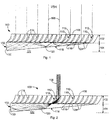
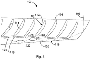
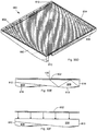
- Figs. 1 and 2 show a cross-sectional view of a first embodiment of a LGSP 100 of the present invention.
- the panel 100 has a light-insertion stage 102 and an optical waveguide stage 104, which can both be made of any suitable optically transmissive material.
- the light-insertion stage 102 receives sunlight 106 at its input surface 108 and from there, the sunlight 106 is guided towards optical elements such as, for example, a series of reflectors 110.
- the reflectors 110 are defined by the interfaces 112 between the optically transmissive material of the light insertion stage 102 and the material making up areas 114.
- the angle at which the interfaces 112 lie with respect to the impinging sunlight 106 and the ratio of the refractive index of the optically transmissive material of the light-insertion stage 102 to the refractive index of the material of areas 114, are chosen such that the sunlight 106 impinging on the interfaces 112 goes through total internal reflection.
- the material 114 is air or any other suitable gas; however, any other suitable material can also make up the material 114.
- the materials of the light-insertion stage 102 and of the optical waveguide stage 104 can include, for example, any type of polymer or acrylic glass such as poly(methyl-methacrylate) (PMMA), which has a refractive index of about 1.49 for the visible part of the optical spectrum. Any other suitable material can also be used.
- the angle at which the interfaces 112 lie with respect to the impinging sunlight 106 ranges from the critical angle to 90°, as measured from the surface normal of the interface 112 (e.g., for a PMMA-air interface, the angle is comprised substantially between about 42.5° and 90°).
- the wall 118 has a first surface 120 between the optically transmissive material of the optical waveguide stage 104 and the material 122, which lies on the other side of the wall 118.
- the angle at which the interface 118 can lie with respect to the horizontal is in the range of 1-5°; however, any other suitable angle will also work.
- the orientation of the wall 118 with respect to the sunlight 106 coming from the apertures 116, and the ratio of the refractive index of the optically transmissive material of the optical waveguide stage 104 to the refractive index of the material 122, are chosen such that the sunlight 106 impinging on the first surface 120 goes through total internal reflection.
- the material 122 can be air or any other suitable gas; however, any other material having a refractive index lower than that of the optical waveguide stage 104 can also make up the material 122.
- the materials of the light-insertion stage 102 and of the optical waveguide stage 104 can include, for example, any type of polymer or acrylic glass such as PMMA. Any other suitable material can also be used.
- each reflecting element 124 is defined by an interface 126 between the optically transmissive material of the optical waveguide stage 104 and the material making up area 128, which can be the same material as that of areas 114.
- the orientation of the reflecting elements 124 with respect to the sunlight 106 coming from the first surface 120, and the ratio of the refractive index of the optically transmissive material of the optical waveguide stage 104 to the refractive index of the material 128, are chosen such that the sunlight 106 impinging on reflecting elements 124 goes through total internal reflection.
- each reflecting element 124 is planar and lies at a non-parallel angle (e,g., 1-5°) to the input surface 108. Additionally, each reflecting element 124 lies at a substantially same distance from the input surface 108 and is substantially parallel to the first surface 120.
- the optical waveguide stage 104 as shown at Figs. 1-3 , generally has the shape of a wedge, which acts to propagate the sunlight 106 being input in the optical waveguide stage 104 through the optical output apertures 116 in the direction where the wedge widens, which is referred to as the downstream direction.
- the optical waveguide stage 104 is such that after multiple successive total internal reflections at the first surface 120 and at the reflecting elements 124, the sunlight 106 reaches an output surface 130 ( Figs. 1 and 2 ), which is part of a sidewall 132, where a SEC (not shown) of any suitable type can be disposed to harvest the energy carried by the sunlight 106.
- Figs. 1 and 2 show the sidewall 132 as being non-perpendicular to the input surface 108; however, the sidewall 132 can lie at any suitable angle from the input surface 108. Further, as will be understood by the skilled worker, the LGSP 100 can have any suitable number of reflecting elements 124 and any suitable number of output optical apertures 116.
- Fig. 3 shows the embodiment where each reflecting element 114 is parallel to the wall 118.
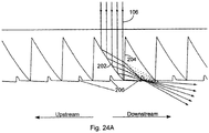
- the angle of incidence remains constant as a ray of sunlight 106 propagates in the downstream direction.
- Fig. 4 shows that the reflecting elements 124 can be formed such that sunlight 106 coming from the first surface 120 ( Fig. 1 ) and propagating towards the light-insertion stage 102 will be reflected off a reflecting element 124 and not impinge on an output optical aperture 116.
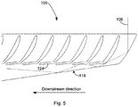
- Fig. 5 shows another embodiment of the present invention where the angle between the wall 118 and the reflecting elements 124 is not parallel but opens in the downstream direction. In this embodiment, it can be shown that the sunlight 106 will remain trapped in the optical waveguide stage 104.
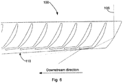
- Fig. 6 shows an embodiment where the angle between the wall 118 and the reflecting elements closes in the downstream direction. In this embodiment, it can be shown that the sunlight 106 eventually transmits out of the optical waveguide stage 104.
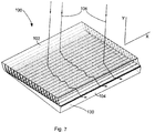
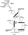
- Fig. 7 shows a perspective view of a LGSP 100 that can have the cross-section shown at Fig. 1 .
- the LGSP 100 of Fig. 7 concentrates the sunlight 106 on the sidewall 132.
- the embodiment of the LGSP 100 of Fig. 7 can be referred to as having a linear geometry since the reflectors 110 all lie along parallel lines.
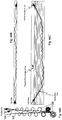
- the performance of the LGSP 100 of Fig. 7 is substantially invariant to changes in the angle of incidence of the sunlight 106 in the plane defined by the X and Y axes. This invariance is shown at Figs. 8A-8C where rays 134 and 136, respectively incident on the input surface 108 at 30° and 45° are directed to the optical waveguide stage 104 by the light-insertion stage 102, and propagate downstream in the optical waveguide stage 104 towards the output surface 130. Because of this invariance to angle of incidence in the X-Y plane, the LGSP 100 of Fig. 7 can be used in conjunction with any suitable single axis sun tracker to effectively concentrate the sunlight 106 to an edge of the panel, i.e., to the output surface 130. As will be understood by the skilled worker, a single axis tracker keeps the panel in a constant alignment with the sun so as to maximize the amount of sunlight captured by the LGSP 100.
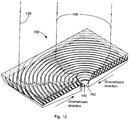
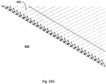
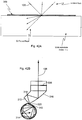
- Fig. 9 shows a perspective view of another LGSP 100 that can have the cross-section shown at Fig. 1 .
- the LGSP 100 of Fig. 9 is substantially shaped as a discus 138 and concentrates the sunlight on an inner wall 140 formed in the hub region of the discus 138, the inner wall 140 acting as an output surface 142, which can be optically coupled, through any suitable way, to any suitable SEC. Examples of how the sunlight 106 can be coupled to a SEC are discussed further below.
- the embodiment of the LGSP 100 of Fig. 9 can be referred to as having a revolved geometry since the reflectors 110 lie on concentric circles.
- SECs include, for example, photovoltaic detectors, solar cells, fiber-optic collectors which gather incident sunlight and transmit it by fiber-optics to the interior of a building for use in lighting fixtures and thermal collectors such as for heating water, or any combination thereof.
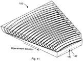
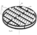
- the LGSP 100 of Fig. 9 can be sectioned off in rectangular panes, as shown at Fig. 10 , or in angular slices, as shown at Fig. 11 , or in any other suitable shape, in order to adapt to any desirable mounting bracket or structure (not shown).
- the LGSPs 100 shown at Figs. 7-11 can be mounted to any suitable type of sun tracking systems such as, for example, single axis tracking systems and dual axis tracking systems.
- design tradeoffs can be made between concentration and angular sunlight acceptance, which in turn determine the required alignment and tracking precision.
- the LGSP 100 of Fig. 7 can achieve, for example, concentrations of 20-50 suns and require single axis solar tracking of approximately 1°.
- the LGSP 100 of Fig. 10 can achieve, for example, concentrations of approximately 500-1000 suns and require dual axis tracking of approximately 1°. Having a larger hub region at the center of the LGSP 100 of Fig. 10 , i.e., having a larger opening at center of the LGSP 100, will produce less concentration than if the hub region were smaller and will require less accurate tracking.
- the ratio of the width of the optical output aperture 116 to the horizontal span of the reflector 110 determines the concentration. If the ratio is made very small, such that the optical output aperture 116 is extremely tight then the concentration can be made very high however the angular acceptance will be very small.
- the ratio between the width of 116 and the horizontal span of 110 also affects the angle of the first surface 120, as a tighter aperture allows for the angle between the surfaces 118 and 108 to be smaller, such as, for example, 1°. This in turn can lead to a smaller sidewall 132, and hence a smaller SEC.
- the light-insertion stage 102 and the optical waveguide stage 104 form distinct layers as shown at Fig. 12 .
- the exit face 144 and the injection face 146 need not be parallel or flat.
- the exit face 144 and the injection face 146 are part of the optical output aperture 116.
- Fig. 13 shows a cross-section of an embodiment of a LGSP not being part of the present invention.
- the sunlight 106 bounces off a first reflector 148, a second reflector 150 and a third reflector 152 before being input into the optical waveguide stage 104 at the output optical aperture 116.
- the first, second and third reflectors are optical elements and can have any suitable shape such as, for example, flat, parabolic, hyperbolic, elliptical and round surfaces.
- any suitable optical elements such as, for example, lenses, Fresnel lenses, parabolic troughs, Cassegrain optics, Winston cones and tapered prisms can also be included in the light-insertion stage 102.
- the optical elements need only be able to deliver the sunlight 106 to the optical output apertures 116 in the general downstream direction of the optical waveguide stage.
- the optical waveguide stage 104 can be independent of the embodiment of the light-insertion stage 102, i.e., a same optical waveguide stage 104 can be used for different embodiments of the light-insertion stage 102.
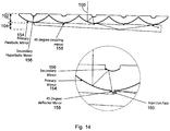
- Fig. 14 shows an embodiment not being part of the invention of the light-insertion stage 102 having a Cassegrain optic design.
- a parabolic primary mirror 154 and a hyperbolic secondary mirror 156 are used to focus and direct the sunlight 106 at a flat reflector 158.
- the sunlight 106 reflects off the reflector 158 and enters the optical waveguide stage 104 at the injection face 160, which acts as an optical output aperture of the light-insertion stage 102.
- the embodiment of Fig. 14 can be used in a linear or revolved geometry LGSP.
- the Cassegrain optics of Fig. 14 require mirrored surfaces on the primary and secondary mirrors (154 and 156 respectively), as well as on the flat reflector 158.
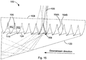
- Fig. 15 shows a light-insertion stage 102 not being part of the invention having a series of Winston cones 162 defined by the interfaces 164A and 164B that lie between the optically transmissive material of the light-insertion stage 102 and the material 166, which can be air or any other suitable gas; however, any other suitable material can also make up the material 166.
- the geometry of the interfaces 164 with respect to the impinging sunlight 106 and ratio of the refractive index of the optically transmissive material of the light-insertion stage 102 to that of the refractive index of the material 166, are chosen such that the sunlight 106 impinging on the interfaces 164 goes through total internal reflection.
- the sunlight 106 impinging on the interface 164A is reflected towards a reflector 168, which in turn directs the sunlight 106 at the optical output aperture 116.
- the sunlight 106 impinging on the interface 164B depending on where on the interface 164B it reflects, it will either be reflected directly to the optical output aperture 116 or to the reflector 168, which will reflect it towards the optical output aperture 116.
- the sunlight 106 impinging directly on the reflector 168 it is also directed at the output optical aperture 116.
- the sunlight 106 After having entered the optical waveguide stage 104 through the optical output aperture 116, the sunlight 106 can either impinge on the first surface 120 or on the reflecting element 124, either way, the sunlight 106 undergoes total internal reflection and is propagated in the downstream direction.
- the reflector 168 can have any suitable geometry such as, for example, a rounded geometry, and can include any suitable type of mirrored coating.
- the light-insertion stage 102 of Fig. 15 can be used in a linear or revolved geometry LGSP.
- the light-insertion layer 102 of Fig. 15 can be used in non-tracking solar panels due to its relatively wide sunlight acceptance angle.
- increased concentration can be obtained by reducing the height of the optical waveguide stage 104 adjacent the output optical aperture of the optical waveguide stage.
- the optical waveguide stage 104 propagates the sunlight 106 by total internal reflection of the sunlight.
- the sunlight will escape from the optical waveguide stage.
- this limitation does not apply to the last reflection within the optical waveguide stage since at this point, the sunlight is about to exit the optical waveguide stage 104.
- the sunlight can be reflected at any suitable angle provided it still reaches the optical output aperture of the optical waveguide stage.
- the SEC will harvest the sunlight, the angle of incidence of the light matters less and, as such, the light can be pinched, or concentrated further, immediately prior to being harvested.
- the additional concentration achievable in this way depends upon the angular spread of the sunlight 106 within the optical waveguide stage 104, with greater concentration being achievable the more collimated the light within the light guide layer is.
- the extra concentration can range, for example, between 1.5 times and 2 times.
- the simplest way to add this extra concentration is to taper the light-guide layer close to the SEC.
- a good taper for concentration is a Winston Cone, which is an off-axis paraboloid, an example of which is shown at reference numeral 170 at Fig. 16 .
- the inclusion of such a Winston cone 170 introduces dead space (defined as LGSP surface exposed to sunlight which does not capture and transmit light to the SEC) in the LGSP 100 because light incident on the Winston cone from above is substantially not captured.
- dead space defined as LGSP surface exposed to sunlight which does not capture and transmit light to the SEC
- a compromise between extra concentration and dead space can be achieved by using a half Winston Cone 172 shown at Fig. 17 .
- a flat faceted taper 174 as shown at Fig. 18 , can be used to approximate the effect of a Winston cone.
- the flat faceted taper does not provide the same additional concentration that can be provided by a Winston cone.
- the approach shown at Fig 18 can be interesting.
- the increased concentration described above can be achieved using a separate optical element, a pinch, which is made of an optically transmissive material and can be secured between the optical waveguide stage and the SEC (not shown). Such a pinch is shown at reference numeral 176 at Fig. 18 . If the refractive index of the pinch 176 is greater than that of the optical waveguide stage, then further additional concentration can be gained. The additional concentration occurs because sunlight deflection occurs at the interface 180 between the optical waveguide stage and the pinch 176, and because the critical angle with a high index material (pinch 176) is lower.
- An advantage of placing an optical element such as, for example, a pinch 176, between the optical waveguide stage and the SEC is that it can insulate the optical waveguide stage against heat accumulation at the SEC. This becomes important if the SEC becomes hotter than what can be withstood by the material of which the optical waveguide stage is made during worst-case operation.
- FIG. 19 Another embodiment of the LGSP 100 of the present invention is shown at Fig. 19 .
- This embodiment allows the optical waveguide stage 104 to provide sunlight to a series of SECs secured to a series of walls 182 defined by the optical waveguide stage 104.
- the use the plurality of walls 182 make for a thinner optical waveguide stage 104.
- a cladding layer 184 can be applied to the input surface and/or to first surface.
- the cladding layer can have a refractive index lower that the refractive index of the light-insertion stage and lower than that of the optical waveguide stage. Further, the cladding layer 184 can also be applied to all spaces within the LGSP 100 that are usually occupied by air or gas.
- the advantage of having such a cladding layer 184 is that it can protect the integrity of the LGSP. With such a cladding layer 184 present, the outer surface of the cladding may become dirty or scratched without compromising the function of the LGSP.
- the cladding layer 184 can be made of any suitable material such as, for example, fluorinated ethylene propylene. As will be understood by the skilled worker, the thickness of the cladding layer can relatively thin and still be effective.
- the LGSP embodiments presented above are scalable. That is, their dimensions can all change by a common factor without affecting the functioning of the optics, provided that the optics do not become so small that interference effects dominate. Such interference effects can become important when the spacing between staggered optical elements is on a scale comparable to the optical wavelengths.
- the most energetic wavelength portion of the solar spectrum is between 0.2 microns and 3 microns. Accordingly, the staggering period of the optical elements and the apertures as well as the size of the apertures can be kept larger than 3 microns to mitigate interference effects.
- the thickness of the optical waveguide stage will largely be limited by the size of the SECs (e.g., the size of PV cell strips) disposed to harvest the sunlight. In the case of PV cell strips, their size can vary, for example, from 1 millimeter to 1 centimeter, although larger or smaller PV cells would work equally well.
- the light-insertion stage (insertion layer) on the other hand can be made as thin as interference effects and fabrication methods can allow.
- the LGSPs of the present invention can be fabricated by molding techniques such as injection molding, compression molding, injection-compression molding or by any other suitable methods. Generally speaking, parts made by molding cannot have undercuts, and as such it is not possible to mold the entire light-guide panels described above at once using conventional molding. However, the LGSP can be manufactured by dividing them into sections that can be molded individually. Two exemplary approaches for sectioning a LGSP for purposes of manufacturing are described below.
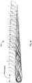
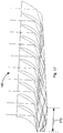
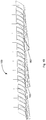
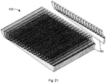
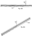
- a first approach is to manufacture thin vertical sections, or slices, of the LGSP and assemble them side by side as shown at Fig. 21 .
- the separate slices 190 of the panel can be held together by an external bracing (not shown), or they can be glued or otherwise bonded together.
- This first approach (slice approach) is suitable for the linear geometry LGSPs.
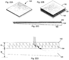
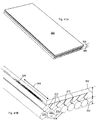
- a second approach is to fabricate horizontal slabs that can be stacked one on top of the other to make a LGSP.
- Such panels can be self-supporting, requiring little in the way of framing and enclosures, and can be such that no gluing or bonding is necessary.
- the slabs make up the functional layers previously described (light-insertion stage and optical waveguide stage); however, a given functional layer can be made up of any number of slabs.
- Figs. 22A-22D show one way to divide the LGSP 100 into three sheets with no undercuts.
- the top two sheets 192 and 194 act in concert to form the insertion layer (light-insertion stage 102), and the bottom sheet 196 forms the light-guide layer (optical waveguide stage 104).
- the embodiment shown at Figs. 22A-22D is similar to that shown at Fig. 13 .
- the sunlight 106 reflects by total internal reflection (TIR) off a parabolic reflector, it then exits the top slab 192 and enters the middle slab 194, then reflects by TIR off two flat facets before exiting the middle slab 194 and entering the bottom slab 196, which acts as the light-guide layer (optical waveguide stage 104).
- TIR total internal reflection
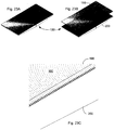
- Figs. 23A-23C show another potential division of the LGSP 100 into two slabs 198 and 200.
- the insertion layer and the light-guide layer are made with one slab each, slabs 198 and 200 respectively.
- sunlight 106 totally internally reflects off a parabolic surface 202 and then exits through a flat facet (exit surface) 204 into the air before encountering an injection face 206 of the light-guide layer (optical waveguide stage).
- Deflection at the exit surface 204 of the insertion layer slab alters the focal point of the parabolic reflector; it moves the focal point slightly upstream, which in turn requires moving the apertures of the light guide layer upstream.
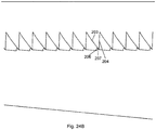
- Fig. 24B shows another embodiment of a light-guide solar panel similar to the one of Fig. 24A but instead with a cubic surface 203 abutting the projection 207 formed by the injection face 206.
- Fig. 24C shows exemplary dimensions for the periodic unit of the light-insertion stage of Fig. 24B , the unit in question comprising the cubic reflector 203, the flat facet 204, the injection face 206 and the projection 207.
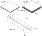
- Figs. 25A-25C shows yet another division of the LGSP 100 into two slabs 208 and 210 which improves on the limitation of the embodiment of Fig. 24A with respect to non-optimal single axis tracking, and allows for the fabrication of a linear geometry LGSP that does not use deflection to concentrate sunlight.
- sunlight 106 is totally internally reflected off the parabolic reflector 212, but in this embodiment it exits the insertion layer slab at an exit face 214 that is the arc of a circle centered on the focus of the parabolic reflector 212.
- the sunlight rays that are converging on the focus of the parabolic reflector each encounter the arc exit face at substantially a right angle, and so no deflection occurs.
- All the above-mentioned slabs can be molded with assembly features that ease the alignment between them when they are assembled into LGSPs.
- the assembly features can have minimal or no interference with the optical performance.
- embodiments of the LGSP of the present invention can be designed so that the backside of upstream apertures rests against the bottom of parabolic reflectors; this is the embodiment shown at Fig. 25C .
- Other assembly features can include small nubs, scattered over the surface of the light-guide layer, which hold the parabolic reflectors in place with respect to the optical waveguide stage 104.
- the space between the slabs should substantially clear of dust and moisture.
- the slabs can be sealed to each other using silicone or any other suitable material, or by using a gasket or any other suitable seal.
- a small amount of desiccant can be added between the slabs to absorb moisture.
- a dust jacket or full envelope can be added to the LGSP to keep it clean and allow for color matching with architecture.
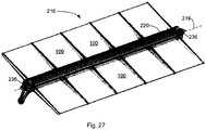
- a single axis tracking solar panel system 216 is shown at Fig. 27 .
- the solar panel system 216 can use LGSPs 100 manufactured using the two-slab approach described above, and can be assembled to tilt about the axis 218.
- the LGSPs 100 can be made in squares, 125 millimeters each side.
- the light-guide layer (optical weveguide stage) can use a half Winston Cone to concentrate the light onto PV cells that are 3 mm tall. The optical concentration of such a system is roughly 30 suns.
- the system 216 is formed using several solar panels 100, for example 10, arranged in two parallel rows on either side of a heat sink 220, which can be made of aluminum of any other suitable material, and in such a way as to concentrate light towards the inner edge of the panels where they connect to the heat sink 220. PV cells are placed between the optical panels 100 and the heat sink 220.
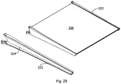
- the solar panels 100 can be kept in alignment, for example, by ribs 222 shows at Fig. 28 .
- the ribs can be made of injection-molded polymer, although machined aluminum or any other material can be used.
- the ribs 222 mechanically hold the panels 100 in position against the heat sink 220 and features on both the ribs 222 and the heat sink 220 can be included to facilitate assembly. Such features (e.g., recess 224) and details of the rib 222 and heat sink 220 are shown at Figs. 28 and 29 respectively.
- the ribs 222 can be held in place against the heat sink using mechanical fasteners, adhesives, or any other suitable means.
- This heat sink 220 can serve two functions: (1) it aids in dissipating heat from the PV cells and (2) it creates a rigid supporting axel for the LGSPs 100.
- the weight of the panels is balanced on either side of the heat sink 220 and the heat sink 220 is where the panel connects to an external supporting frame.
- the heat sink 220 can have fins 226 made of a folded aluminum piece bonded between two extruded aluminum rails 228. The fins are connected to the two rails and create vertical air channels 230 in heat sink 220.
- the bond between the fins and the two rails can be made by brazing, epoxy, swaging or by any other means.
- This open heat-sink embodiment allows heat to be dissipated by natural convection as hot air can rise out of the heat-sink 220 and cooler air may enter into the heat-sink 220 from below.
- PV cells used in the system 216 can be of any size, such as 125 millimeters by 125 millimeters, and can be cut into strips of any height, for example, 3 mm tall for use with this embodiment.
- the PV cells can be encapsulated in any conventional way. For example, they can be soldered together in series and then encapsulated with ethylene vinyl acetate (EVA) or any other suitable material. Alternately, the electrical connections of the PV cells can be made by soldering, adhering or bonding the PV cells to a patterned circuit on a thermally conductive dielectric substrate. Insulated metal substrates (IMSs) such as those sold by The Bergquist Company of Chanhassen Minnesota would be appropriate.
- Fig. 30 shows an IMS substrate 232 soldered to a PV cell 234; the solder layer is shown at 235.
- the IMS 232 can be connected to the aluminum heat sink 220 by epoxy or adhesive, or by any other suitable means.
- a typical IMS 232 has electrical patterning of copper on top of a polymer insulating layer which is bonded to an aluminum or copper base. It is possible to forgo the base and affix the electrically patterned polymer-insulating layer directly to the heat sink 220. This process can be done in an oven by heat curing. An advantage of this approach is that it eliminates the base element and can reduce costs.
- the PV cell 234 can be bonded to the IMS 232 through a conductive ribbon or mesh that is connected to the entire length of the topside connector (not shown) of the PV cell 232.
- the backside connector of the PV cell 232 can be bonded over its entire length and/or surface as well. For PV cells 232 that are long and narrow and fragile, using the connection method described above allow the PC cells to break in sections without losing their functionality or substantially affecting the power production.
- PV cells can be encapsulated to protect against moisture to avoid corrosion. This can be done using any suitable encapsulant such as, for example, ethylene vinyl acetate (EVA).
- EVA ethylene vinyl acetate
- EVA requires heat curing and so, the parts requiring sealing need to be placed in an oven.
- Another approach is to use an encapsulant, which cures in place at room temperature.
- Certain optically clear adhesives such as the silicone Sylgard184 by Dow Corning, can serve this purpose and can be poured in a thin layer on top of the PV cells after soldering.
- the panels can be fixed in place before the silicone has begun curing. This seals the space between the panels and the PV cells and creates an optical bond between them. The optical bond between the optical panels and the PV cells diminishes Fresnel losses at the exit edge of the optical panel.
- the LGSPs can be arranged on a mounting frame to form a solar power system.
- the heat sinks can connect with bearings on the mounting frame, which allows for free rotation of the pane! about the axel made by the heat-sink 220 (see axis 218 at Fig. 27 ).
- the heat sink 220 can connect to the bearings by way of injection molded end caps (236, Fig. 27 ), which are joined to the ends of the heat sink 220.
- These end caps 236 can have any suitable features that allow connection to the bearings on the frame.
- the end caps 236 can be joined to the heat-sink either mechanically, with epoxies, adhesives, with adhesive tape, or through any other suitable means.
- the end caps 236 of the heat-sink 220 are also coupled to a mechanism that allows an actuator to control the rotation of the LGSPs 100.
- a mechanism that allows an actuator to control the rotation of the LGSPs 100 For example, as shown at Fig. 31 , three bar linkages can connect all the modules to a single rail 238 that is driven by a linear actuator 240.
- each LGSP can have a pinion gear which attaches to a rack, which is again driven by a linear actuator.
- a single linear actuator moving the single rail can drive the motion of all the panels, so that they will tilt in unison and maintain alignment.
- Full sunlight tracking solar panel systems can be made using LGSPS having a revolved geometry and manufactured using the two-layer approach exemplified at Figs. 23A-23C .
- the external appearance of such full tracking systems can be similar to those described for the single axis tracking system above in that LGSPs can be arranged along either side of a central heat-sink and supported by ribs.
- the external dimensions of the panels can be 125 millimeters by 250 millimeters.
- Sunlight is concentrated to a line 242 at the center of the inner edge of the LGSP as shown at Figs. 32A and 32B .
- Sunlight exits the solar panel 100 at a half cylindrical facet 244 and enters an air gap. While in principle a thin PV cell could be placed along the line 242, such an arrangement would have limited angular acceptance.
- a wider angular acceptance is achieved by placing a 90° roof prism 246 into the half cylindrical facet, as shown at Figs. 33A-33C .
- This roof prism 246 can be made of glass or of any other suitable material, and can have an index of refraction greater than 1.4.
- High efficiency PV cells such as triple-junction cells, can be bonded optically to the base 248 of the roof prism using a silicone encapsulant or another optical epoxy.
- Figs. 33D-33G show how a rectangular light-guide solar panel 800 can be made using two light-insertion stage sections 802 and 804 each having a revolved geometry and a corresponding optical waveguide stage section 806 and 808.
- Sunlight impinging on the light-insertion stage 802 is coupled to the optical waveguide stage 806, which propagates the sunlight to the surface 810.
- the optical waveguide stage 808 which propagates the sunlight to the surface 812.
- the surfaces 810 and 812 can be flat surfaces and any suitable SECs can be secured thereto. By not having to use a prism to couple the light exiting from the optical waveguide stages 806 and 808, Fresnel reflections losses can be avoided.
- the optical waveguides 806 and 808 can have half-Winston cone profiles 816 and 818 such as shown at Fig. 33E. Fig.
- Fig. 33F shows that the light-guide solar panel 800 can be made in a two-layer process by laying the light-insertion stages 802 and 804 over the optical waveguide stages 806 and 808.
- Fig. 33G shows an exploded view of the assembly of Fig. 33E . Given that sunlight emerges from both sides of the optic, heat sinks can be placed on respective opposite sides of the panel. Because this panel of Figs. 33D does not have a coupling prism, the portion of the optical waveguide stages 806 and 808 that is adjacent the surface 810 and 812 can be made of an insulating material, which can withstand more heat, such as, for example, fused silica, while the remainder is made out of PMMA.
- LGSPs using a revolved geometry and designed for high solar concentration offer better performance when used in conjunction with full tracking of the sun, maintaining the sun's rays parallel to the normal vector of input surface of the solar panel to within +/-1°.
- the full tracking can be achieved several ways, but two methods in particular lend themselves to the system.
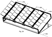
- the first full tracking method is shown at Fig. 34 where the LGSPs 100 are mounted in a frame 249 to tilt about a first series of axes 250 and the frame 249 can tilt about an axis 252, which is substantially orthogonal to the axes 250.
- the LGSP can roll east-west to track the sun's movement over the course of the day and the frame can tilt north-south to adapt to the seasonal variation of the sun.
- the LGSPs 100 can be arranged in frames 254 or 256 and can tilt about the axes 258 and 260 respectively. Further, the frames 254 and 256 can be made to rotate about the axes 262 and 264 respectively.
- Fig. 37 shows a variant of the LGSP employing Winston cones in the insertion layer (light-insertion stage 102), as shown at Fig. 15 .
- the embodiment of Fig. 37 which is a linear geometry embodiment, is well suited for non-tracking applications because it has a wide angular acceptance because of the Winston cones.
- a bifacial PV cell 266 positioned between two optical panels; this embodiment doubles the concentration.
- the LGSP 100 of Fig. 37 can be made in a two part stack, but rather than molding a solar panel for each PV cell strip, a cluster of panels can be molded, a cluster of optical panels being a grouping of a number of concentrator optics into fewer pieces.
- Fig. 38 shows how a cluster LGSP 268 can be made to accommodate four PV cells 266.
- the slab 270 that forms light-guide layers can have grooves 272 molded into it to accommodate bifacial PV cells 266.
- the PV cells 266 can be soldered and then encapsulated before being placed in the groove, or they can be only soldered together to form a circuit and then placed in the groove and encapsulated in place using a cast in place encapsulant such as clear silicone or any other optical epoxy.
- Attaching a number of cluster panels together makes for a full solar panel module.
- One method is to use an aluminum framing grill to tie all the panels together.
- Another method is to array and bond the optical panels by any suitable means onto a stiff superstrate of glass or of any other suitable material.
- the non-tracking LGSP 268 will generally not have 180° of angular acceptance in the cross sectional plane of the optics as seen at Fig. 37 .
- the cone of acceptance of the LGSP 268 can be +/-30° from the normal of the panel, which is sufficient to accommodate the seasonal variation of the sun's position in the sky.
- the non-tracking LGSP 168 should be installed at a tilt which matches the latitude of the installation location; this would ensures that the normal to the panel's input surface is parallel with the sun's rays at equinox.
- this does limit the installation configurations of the non-tracking LGSP 268.
- the LGSP 268 can be designed with their cone of acceptance tilted off the normal as shown at Fig. 39 for northern hemisphere locations.
- a finite number of non-tracking LGSPs 268 series can be designed to accommodate any installation configuration.
- roll-to-roll continuous casting or embossing can be used to fabricate the light-insertion stage optics as films. It is possible to use roll-to-roll manufacturing methods because all of the above solar panels are composed of a stack of slabs that have no undercuts.
- the wedge-shaped light-guide layer optical waveguide stage
- the light-insertion stage can be applied to the optical waveguide stage using a lamination process or any other suitable process.
- the light-insertion layer 102 of the LGSP of the present invention can also use any suitable type of lenses as optical elements instead of just the focusing TIR interfaces described above.
- Fig. 40 shows a LGSP 100 not being part of the present invention having a series of lenses 274 that focus and optically couple the sunlight 106 to the optical waveguide stage 104.
- the LGSP 300 has an insertion layer (light-insertion stage 302) and a light-guide layer (optical waveguide stage 304).
- the light-insertion stage 302 has optical elements in the form of a deflector section 306 and reflector sections 312.
- the deflector section 306 deflects impinging sunlight 106 in one or both of the directions indicated by the double-arrow 308.
- the deflected sunlight is directed towards the optical elements that are the reflector sections 312, which are shaped as a series of focusing tapered light channels.
- the tapered light channels are optically coupled, through a series of optical output apertures 313 to a series of waveguides 314 that form the optical waveguide stage 304.
- the deflector section 306 can include an optical directing layer in the form of a Volume Phase Hologram (VPH). Fringes in the VPH hologram are formed in any suitable manner, using the interference between two coherent UV light sources. The fringe spacing and angle can be designed such one or more modes of diffraction can fall within 45 degrees of the plane of the solar panel 300.
- Fig. 42A shows an example of how such a VPH 309 operates. The resulting deflection is exemplified at Figs. 42B to 42D .
- the deflector section 306 can also be made using non-interference optics, such as, for example, flat faceted optics like prisms. For instance, an array of 60° prisms arranged in an interlocking manner with a small air gap in between them would split light incident into the plane of the panel in two directions. This bi-directional deflection would lead to light accumulating on two opposite edges of the solar panel 300. Such directing optics are shown at Fig. 43 .
- the optical waveguide stage 304 has a linear geometry and can have a plurality of waveguides 314 that receive light from their respective tapered light channels (reflector section 312) and that trap light by total internal reflection.
- the waveguides 314 act as delay lines whereby light enters from above, at optical output apertures 313, travels for some distance and then can exits out the top through the optical output apertures 313.
- a potential channel embodiment is shown at Figs. 42A-42C .
- Light entering a tapered light channel (reflector section 312) is reflected off a first parabolic section 316, then off a flat face 318 and off a second parabolic section 320 before entering into a cylindrical section, which defines the waveguide 314.
- the light can travel within the waveguide 314 in a spiral manner for some distance before escaping out.
- the length of the waveguide 314 is less than the mean travel distance of the trapped light rays, light coupled into the waveguide 314 will emerge concentrated from the end of the channel where it can be harvested by any suitable SEC.
- the optical waveguide stage 104 is 1 cm tall, and the waveguides 314 are 150 cm long then 75% of the light incident on the LGSP 300 will reach the two ends of the waveguide for harvesting by an SEC. If light is incident evenly on the LGSP 300 then light will be distributed evenly between the two ends of the waveguide channel.
- the LGSP 300 can include any number of waveguides 314 and tapered light channels 312 and each waveguide 314 can form a unit with a respective tapered light channel 312.
- the units formed by the tapered light channel 312 and their respective waveguides 314 can be made by molding.
- each waveguide 314 has an output surface 315, and the sum of the output surface 315 form the total output surface of the optical waveguide stage 304.
- Any suitable SEC can be placed at the output of the plurality of optical output apertures 315 to harvest the sunlight 106.
- Figs. 44A-44C shows a tapered light channel 322 having a plurality of waveguides 326 formed thereon, with the diameter of the waveguide decreasing as the width of the tapered light channel decreases.
- the staggering of the waveguides vertically allows for two or more channels to be positioned closely side by side with little dead space in between them.
- the heat sink 220 previously described can be used in conjunction with single axis tracking systems and the full tracking high concentrator systems to shed excess heat from the SEC (e.g., PV cells) into the surrounding air. However, the excess heat can instead be used to heat water. This functionality can be accomplished with the heat sink 400 shown at Figs. 45A and 45B .
- the heat sink 400 can be made of aluminum or any other suitable material.
- the heat sink 400 has one or more channels 402 for flowing water which extracts excess heat generated at the SECs.
- end caps 403 can be affixed to the heat sink 400 and serve the dual purpose of securing LGSPs to a mounting frame via bearings, and they also serve as inlet and outlets to a heat exchanger (not shown).
- Water could either flow straight through a heat sink 400, with an inlet on one end cap and an outlet on the other, or it could flow in and out of the heat sink 400 through the same end-cap, with the opposite end cap serving as a u-bend.
- This embodiment can simplify hose routing between many modules in an extended system. The number of channels in the extrusion could be increased so as to have a larger surface area of contact between the water and the aluminum of the heat sink 400.
- the rate of water flow through the heat sink 400 can be used to control the temperature of the SECs and be used to keep the LGSPs within their operating temperature range.
- a system using heat sinks 400 interconnected through hoses 406 is shown at Fig. 46 .
- a heat exchange fluid other than water can be used in the system of Fig. 46 .
- Sunlight captured by the LGSP of the present invention can be used in a solar thermal system that does not use PV cells.
- An example of such a solar thermal system 500 is shown at Fig. 47 .
- the system 500 can use a double walled tube 502 that has its outermost tube transparent.
- An insulating gas, such as argon, would separate the inner tube from the outer tube.
- the inner tube can be black so as to absorb incident sunlight.
- a heat absorbing liquid such as water, oil, or any other suitable liquid flows.
- the tube 502 is placed in the position previously occupied by heat sinks in the above-described embodiments.
- the concentrated sunlight passes through the clear outer tube, and the insulating gas layer, and is absorbed by the inner tube. This causes the liquid in the inner tube to heat.
- the fluid carrying tubes can remain fixed in position while the optics rotate about them.
- the LGSP of the present invention is relatively insensitive to thermal expansion or contraction. This is possible because all the optical components of the solar panels are made of similar, if not the same, materials. Because of this, they will expand by the same degree and the function of the optical element will not change significantly. Specifically, as the reflectors 110 expand, so too will the waveguide section 104. This maintains the same focus for light 106 reflecting of 110 and focusing on 116 from figure 1 as the unit expands and contracts with changes in temperature.
- the panel is tilted to maintain alignment in one plane with incident sunlight. It is also possible to add an optical device on top of the optics that preconditions the light, altering the angle of the incident light to align the incident light to the optics. Such preconditioning optics could employ moving mirrors, prisms, or electro-optics.
- Tracking can be accomplished manually by occasionally tilting the single axis tracking panel, or the non-tracking panel.
- a manual-tracking panel would be one with a wide enough angular acceptance, say, for example, plus or minus 5 degrees in the cross-sectional plane, so that it would only need to be re-aligned slightly by hand every few weeks.
- Electronic alignment sensors could assist in the alignment, but actuators would not be needed.
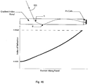
- a LGSP using a different mechanism can be made using a panel with a gradient index of refraction.
- the refractive index gradient increases in the downstream direction of the LGSP, so that light incident on the panel would deflect towards the downstream direction. If the gradient was sufficient to cause enough deflection for TIR to occur at the bottom face of the panel then the light would be trapped and would become conducted down to the edge of the panel as shown at Fig. 48 .
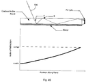
- a mirror may be required for the first reflection if light exits the bottom face of the panel, and further deflection while traveling back up through the panel to the top surface would increase the angle of incidence on the top face enough for TIR to occur. This is shown at Fig. 49 .
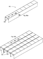
- Figs. 50A and 50B shows how light-guide solar panels such as the light-guide solar panel 800 of Fig. 33D can be grouped together.
- the light-guide solar panels 800 can be placed between two vertically oriented aluminum heat sinks 900 to form a linear assembly 902 of light-guide solar panels 800. Larger groups of light-guide solar panels 800 can be assembled by joining together the linear assemblies 902.
- the present invention is that of a solar energy system that uses a LGSP to trap light inside a dielectric or other transparent panel and propagates the light to one of the panel edges for harvesting by a SEC.
- This allows for very thin modules whose thickness is comparable to the height of the SEC, for example a PV cell, at the edge of the module, thus eliminating the depth requirements inherent in traditional solar energy systems such as CPV systems.
- Light striking the LGSP is redirected and trapped internally so that it exits the panel through one of its edges where a SEC receives it.
- LGSPs can be combined in clusters to make modules.
- the LGSP optics can be designed structurally to be largely self-supporting, meaning that they do not require an external enclosure to maintain their shape and orientation. A full enclosure can be added to the embodiment.
- LGSP modules can be supported by a minimal axle-and-rib configuration.
- Concentrated sunlight may be harnessed for a purpose other than creating electricity with PV cells.
- One alternate use is the heating of an element.
- the modules can also be configured to heat water while simultaneously generating electricity. It is also possible to couple the concentrated light into a fiber optic or other light-guide to propagate it to another location for some other use, such as to a lighting fixture to provide solar lighting.
- the LGSP optics of the present invention can be used to reduce the thickness of optics in a other applications including, for example, lamps and lighting.
Priority Applications (1)
| Application Number | Priority Date | Filing Date | Title |
|---|---|---|---|
| EP13164469.2A EP2645426A1 (en) | 2007-05-01 | 2008-05-01 | Light-guide solar panel and method of fabrication thereof |
Applications Claiming Priority (4)
| Application Number | Priority Date | Filing Date | Title |
|---|---|---|---|
| US91520707P | 2007-05-01 | 2007-05-01 | |
| US94274507P | 2007-06-08 | 2007-06-08 | |
| US95177507P | 2007-07-25 | 2007-07-25 | |
| PCT/CA2008/000831 WO2008131561A1 (en) | 2007-05-01 | 2008-05-01 | Light-guide solar panel and method of fabrication thereof |
Related Child Applications (1)
| Application Number | Title | Priority Date | Filing Date |
|---|---|---|---|
| EP13164469.2A Division-Into EP2645426A1 (en) | 2007-05-01 | 2008-05-01 | Light-guide solar panel and method of fabrication thereof |
Publications (3)
| Publication Number | Publication Date |
|---|---|
| EP2153475A1 EP2153475A1 (en) | 2010-02-17 |
| EP2153475A4 EP2153475A4 (en) | 2010-07-28 |
| EP2153475B1 true EP2153475B1 (en) | 2017-07-12 |
Family
ID=39925147
Family Applications (4)
| Application Number | Title | Priority Date | Filing Date |
|---|---|---|---|
| EP14001744.3A Withdrawn EP2767754A3 (en) | 2007-05-01 | 2008-05-01 | Illumination device |
| EP08748249A Ceased EP2174058A4 (en) | 2007-05-01 | 2008-05-01 | ILLUMINATION DEVICE |
| EP13164469.2A Withdrawn EP2645426A1 (en) | 2007-05-01 | 2008-05-01 | Light-guide solar panel and method of fabrication thereof |
| EP08748233.7A Active EP2153475B1 (en) | 2007-05-01 | 2008-05-01 | Light-guide solar panel and method of fabrication thereof |
Family Applications Before (3)
| Application Number | Title | Priority Date | Filing Date |
|---|---|---|---|
| EP14001744.3A Withdrawn EP2767754A3 (en) | 2007-05-01 | 2008-05-01 | Illumination device |
| EP08748249A Ceased EP2174058A4 (en) | 2007-05-01 | 2008-05-01 | ILLUMINATION DEVICE |
| EP13164469.2A Withdrawn EP2645426A1 (en) | 2007-05-01 | 2008-05-01 | Light-guide solar panel and method of fabrication thereof |
Country Status (10)
| Country | Link |
|---|---|
| US (6) | US7873257B2 (zh) |
| EP (4) | EP2767754A3 (zh) |
| JP (2) | JP5837746B2 (zh) |
| KR (1) | KR101487896B1 (zh) |
| CN (2) | CN101681949B (zh) |
| AU (1) | AU2008243623B2 (zh) |
| CA (2) | CA2685103C (zh) |
| ES (1) | ES2642209T3 (zh) |
| IL (1) | IL201786A (zh) |
| WO (2) | WO2008131566A1 (zh) |
Families Citing this family (192)
| Publication number | Priority date | Publication date | Assignee | Title |
|---|---|---|---|---|
| US20100024868A1 (en) * | 2006-12-13 | 2010-02-04 | Pythagoras Solar Inc. | Solar radiation collector |
| US9040808B2 (en) * | 2007-05-01 | 2015-05-26 | Morgan Solar Inc. | Light-guide solar panel and method of fabrication thereof |
| US9337373B2 (en) | 2007-05-01 | 2016-05-10 | Morgan Solar Inc. | Light-guide solar module, method of fabrication thereof, and panel made therefrom |
| EP2767754A3 (en) * | 2007-05-01 | 2015-02-18 | Morgan Solar Inc. | Illumination device |
| US7672549B2 (en) * | 2007-09-10 | 2010-03-02 | Banyan Energy, Inc. | Solar energy concentrator |
| US8412010B2 (en) * | 2007-09-10 | 2013-04-02 | Banyan Energy, Inc. | Compact optics for concentration and illumination systems |
| CN101809377B (zh) * | 2007-09-10 | 2013-07-24 | 榕树能量公司 | 用于光能的集中、聚集和照明的紧凑光学装置 |
| ES2326456B1 (es) * | 2008-01-30 | 2010-05-25 | Abengoa Solar New Technologies S.A. | Planta de baja concentracion solar y metodo para maximizar la produccion de energia electrica de sus modulos fotovoltaicos. |
| US20110094563A9 (en) | 2008-05-16 | 2011-04-28 | Baker James T | Solar systems that include one or more shade-tolerant wiring schemes |
| US20100024805A1 (en) * | 2008-07-29 | 2010-02-04 | Genie Lens Technologies, Llc | Solar panels for concentrating, capturing, and transmitting solar energy in conversion systems |
| MX2011002993A (es) | 2008-09-19 | 2011-05-30 | Univ California | Sistema y metodo para captura de energia solar y metodo relacionado de fabricacion. |
| US8730179B2 (en) * | 2008-09-30 | 2014-05-20 | Apple Inc. | Integrated touch sensor and solar assembly |
| US20120024374A1 (en) * | 2008-10-02 | 2012-02-02 | Raydyne Energy, Inc. | Solar energy concentrator |
| AU2008363098A1 (en) * | 2008-10-15 | 2010-04-22 | Kuldip Singh Virk | Solar panels |
| ES2364665B1 (es) * | 2008-11-12 | 2012-05-23 | Abengoa Solar New Technologies, S.A. | Sistema de captación y concentración de luz. |
| JP2010141297A (ja) * | 2008-11-14 | 2010-06-24 | Nippon Leiz Co Ltd | 導光体および光電変換器ならびに平面光電変換装置 |
| TW201023379A (en) * | 2008-12-03 | 2010-06-16 | Ind Tech Res Inst | Light concentrating module |
| US20100165495A1 (en) * | 2008-12-29 | 2010-07-01 | Murtha R Michael | Collection optic for solar concentrating wedge |
| US8327839B2 (en) * | 2009-01-07 | 2012-12-11 | Pratt & Whitney Rocketdyne, Inc. | Air instrumentation system for concentrated solar power generation systems |
| US8266819B2 (en) * | 2009-01-07 | 2012-09-18 | Pratt & Whitney Rocketdyne, Inc. | Air drying system for concentrated solar power generation systems |
| US7968790B2 (en) * | 2009-01-16 | 2011-06-28 | Genie Lens Technologies, Llc | Photovoltaic (PV) enhancement films for enhancing optical path lengths and for trapping reflected light |
| US8338693B2 (en) * | 2009-01-16 | 2012-12-25 | Genie Lens Technology, LLC | Solar arrays and other photovoltaic (PV) devices using PV enhancement films for trapping light |
| US8048250B2 (en) * | 2009-01-16 | 2011-11-01 | Genie Lens Technologies, Llc | Method of manufacturing photovoltaic (PV) enhancement films |
| US7904871B2 (en) * | 2009-01-16 | 2011-03-08 | Genie Lens Technologies, Llc | Computer-implemented method of optimizing refraction and TIR structures to enhance path lengths in PV devices |
| US9105783B2 (en) * | 2009-01-26 | 2015-08-11 | The Aerospace Corporation | Holographic solar concentrator |
| KR101057790B1 (ko) | 2009-02-03 | 2011-08-19 | 테라웨이브 주식회사 | 집광형 태양광 발전 모듈 |
| US20100224248A1 (en) * | 2009-02-20 | 2010-09-09 | John Kenney | Solar Modules Including Spectral Concentrators and Related Manufacturing Methods |
| US20100212716A1 (en) * | 2009-02-20 | 2010-08-26 | Scott Lerner | Solar radiation collection using dichroic surface |
| US8774573B2 (en) | 2009-02-20 | 2014-07-08 | OmniPV, Inc. | Optical devices including resonant cavity structures |
| US20100212717A1 (en) * | 2009-02-20 | 2010-08-26 | Whitlock John P | Solar collector with optical waveguide |
| US20100236625A1 (en) * | 2009-02-20 | 2010-09-23 | John Kenney | Solar Modules Including Spectral Concentrators and Related Manufacturing Methods |
| US20100218807A1 (en) * | 2009-02-27 | 2010-09-02 | Skywatch Energy, Inc. | 1-dimensional concentrated photovoltaic systems |
| WO2010101644A1 (en) * | 2009-03-05 | 2010-09-10 | James Rosa | 3-d non-imaging radiant energy concentrator |
| JP2010212280A (ja) * | 2009-03-06 | 2010-09-24 | Sumitomo Electric Ind Ltd | 太陽電池の導光構造、太陽電池ユニット及び太陽電池モジュール |
| CA2658193A1 (en) * | 2009-03-12 | 2010-09-12 | Morgan Solar Inc. | Stimulated emission luminescent light-guide solar concentrators |
| US8290318B2 (en) * | 2009-04-21 | 2012-10-16 | Svv Technology Innovations, Inc. | Light trapping optical cover |
| US9256007B2 (en) * | 2009-04-21 | 2016-02-09 | Svv Technology Innovations, Inc. | Light collection and illumination systems employing planar waveguide |
| EP2430741A4 (en) * | 2009-05-14 | 2017-06-21 | Sunboost Ltd. | Light collection system and method |
| US20100319684A1 (en) * | 2009-05-26 | 2010-12-23 | Cogenra Solar, Inc. | Concentrating Solar Photovoltaic-Thermal System |
| US8189970B2 (en) * | 2009-06-24 | 2012-05-29 | University Of Rochester | Light collecting and emitting apparatus, method, and applications |
| US7817885B1 (en) | 2009-06-24 | 2010-10-19 | University Of Rochester | Stepped light collection and concentration system, components thereof, and methods |
| US9246038B2 (en) | 2009-06-24 | 2016-01-26 | University Of Rochester | Light collecting and emitting apparatus, method, and applications |
| EP2446306A4 (en) * | 2009-06-24 | 2014-09-10 | Univ Rochester | ATTENUATED LIGHT COLLECTION AND CONCENTRATION SYSTEM, COMPONENTS THEREOF AND METHODS |
| TWI409967B (zh) * | 2009-07-13 | 2013-09-21 | Epistar Corp | 一種太陽能電池模組及其製作方法 |
| TWI482995B (zh) * | 2009-07-20 | 2015-05-01 | Ind Tech Res Inst | 集光裝置及照明設備 |
| WO2011022631A2 (en) | 2009-08-20 | 2011-02-24 | Light Prescriptions Innovators, Llc | Stepped flow-line concentrators and collimators |
| JP5443494B2 (ja) * | 2009-08-21 | 2014-03-19 | 株式会社東芝 | 光学素子および表示装置 |
| JP2011059323A (ja) * | 2009-09-09 | 2011-03-24 | Leiz Advanced Technology Corp | 集光モジュールおよびこれを用いた集光ユニット |
| WO2011038127A2 (en) * | 2009-09-24 | 2011-03-31 | Genie Lens Technologies Llc | Tracking fiber optic wafer concentrator |
| WO2011039356A1 (en) * | 2009-10-01 | 2011-04-07 | Danmarks Tekniske Universitet | Solar energy harvesting system |
| KR20110048406A (ko) * | 2009-11-02 | 2011-05-11 | 엘지이노텍 주식회사 | 태양전지 및 이의 제조방법 |
| US20110017267A1 (en) * | 2009-11-19 | 2011-01-27 | Joseph Isaac Lichy | Receiver for concentrating photovoltaic-thermal system |
| US8937242B2 (en) | 2009-11-24 | 2015-01-20 | Industrial Technology Research Institute | Solar energy system |
| EP2504859A4 (en) * | 2009-11-25 | 2015-05-27 | Banyan Energy Inc | SOLAR PANEL CONSTRUCTION |
| US20110162712A1 (en) | 2010-01-07 | 2011-07-07 | Martin David Tillin | Non-tracked low concentration solar apparatus |
| US20110232719A1 (en) * | 2010-02-17 | 2011-09-29 | Freda Robert M | Solar power system |
| ES2364310B1 (es) | 2010-02-19 | 2012-04-02 | Abengoa Solar New Technologies, S.A | Sistema de concentracion solar fotovoltaica |
| US8673186B2 (en) * | 2010-03-02 | 2014-03-18 | Microsoft Corporation | Fabrication of an optical wedge |
| US20110220173A1 (en) * | 2010-03-09 | 2011-09-15 | Michael Lebby | Active solar concentrator with multi-junction devices |
| WO2011114240A2 (en) * | 2010-03-19 | 2011-09-22 | Morgan Solar Inc. | Solar-light concentration apparatus |
| CN102918660B (zh) * | 2010-04-01 | 2015-11-25 | 摩根阳光公司 | 集成光伏模块 |
| US20110271999A1 (en) | 2010-05-05 | 2011-11-10 | Cogenra Solar, Inc. | Receiver for concentrating photovoltaic-thermal system |
| US8686279B2 (en) | 2010-05-17 | 2014-04-01 | Cogenra Solar, Inc. | Concentrating solar energy collector |
| US8669462B2 (en) | 2010-05-24 | 2014-03-11 | Cogenra Solar, Inc. | Concentrating solar energy collector |
| US8642937B1 (en) * | 2010-05-27 | 2014-02-04 | Exelis, Inc. | Full-aperture, back-illuminated, uniform-scene for remote sensing optical payload calibration |
| US8624612B2 (en) * | 2010-06-15 | 2014-01-07 | Electronic Testing Services, Llc | RF non-contact thin film measurement using two port waveguide |
| US8735791B2 (en) | 2010-07-13 | 2014-05-27 | Svv Technology Innovations, Inc. | Light harvesting system employing microstructures for efficient light trapping |
| CN103038577B (zh) * | 2010-07-30 | 2015-11-25 | 摩根阳光公司 | 光导太阳能模块及其制造方法和由其制成的电池板 |
| DE102010034020A1 (de) * | 2010-08-11 | 2012-02-16 | Fraunhofer-Gesellschaft zur Förderung der angewandten Forschung e.V. | Oberflächenstruktur sowie Fresnel-Linse und Werkzeug zur Herstellung einer Oberflächenstruktur |
| JP2013543215A (ja) * | 2010-09-21 | 2013-11-28 | コーニンクレッカ フィリップス エヌ ヴェ | 狭ビームサイズと高ルーメン出力とを有するセグメント化スポットライト |
| ES2399254B1 (es) | 2010-09-27 | 2013-11-11 | Abengoa Solar New Technologies S.A | Sistema reflexivo de concentracion solar fotovoltaica |
| US8798432B2 (en) | 2010-10-21 | 2014-08-05 | Microsoft Corporation | Fabrication of a laminated optical wedge |
| CA2815671C (en) | 2010-10-28 | 2016-12-13 | Banyan Energy, Inc. | Redirecting optics for concentration and illumination systems |
| CN102544172B (zh) * | 2010-12-30 | 2015-10-21 | 财团法人工业技术研究院 | 聚焦型太阳能导光模块 |
| US8885995B2 (en) | 2011-02-07 | 2014-11-11 | Morgan Solar Inc. | Light-guide solar energy concentrator |
| US9246230B2 (en) | 2011-02-11 | 2016-01-26 | AMI Research & Development, LLC | High performance low profile antennas |
| US9806425B2 (en) * | 2011-02-11 | 2017-10-31 | AMI Research & Development, LLC | High performance low profile antennas |
| DE102011004349A1 (de) * | 2011-02-17 | 2012-08-23 | Automotive Lighting Reutlingen Gmbh | Beleuchtungseinrichtung eines Kraftfahrzeugs |
| US8928988B1 (en) | 2011-04-01 | 2015-01-06 | The Regents Of The University Of California | Monocentric imaging |
| US8791355B2 (en) * | 2011-04-20 | 2014-07-29 | International Business Machines Corporation | Homogenizing light-pipe for solar concentrators |
| US9263605B1 (en) * | 2011-04-20 | 2016-02-16 | Morgan Solar Inc. | Pulsed stimulated emission luminescent photovoltaic solar concentrator |
| JP2012248776A (ja) * | 2011-05-31 | 2012-12-13 | Dainippon Printing Co Ltd | 集光素子及び太陽電池システム |
| ITMI20110994A1 (it) * | 2011-05-31 | 2012-12-01 | Andrea Cincotto | Apparato fotovoltaico |
| US20140183960A1 (en) | 2011-06-22 | 2014-07-03 | Morgan Solar Inc. | Photovoltaic power generation system |
| WO2013011613A1 (ja) * | 2011-07-15 | 2013-01-24 | パナソニック株式会社 | 集光型レンズアレイおよびそれを備えた太陽電池 |
| US8847142B2 (en) | 2011-07-20 | 2014-09-30 | Hong Kong Applied Science and Technology Research Institute, Co. Ltd. | Method and device for concentrating, collimating, and directing light |
| US9108369B2 (en) | 2011-07-25 | 2015-08-18 | Microsoft Technology Licensing, Llc | Wedge light guide |
| JP5569484B2 (ja) * | 2011-07-27 | 2014-08-13 | 三菱電機株式会社 | 集光器および集光器を備えた太陽電池 |
| JP6040242B2 (ja) | 2011-08-15 | 2016-12-07 | モーガン ソーラー インコーポレーテッド | 自己安定型の太陽光追尾装置 |
| KR101347785B1 (ko) * | 2011-08-29 | 2014-01-10 | 정재헌 | 타원체 거울 집속 광 가이드 |
| US9482871B2 (en) | 2011-08-30 | 2016-11-01 | Hong Kong Applied Science And Technology Research Institute Co. Ltd. | Light concentration and energy conversion system |
| US20130071716A1 (en) * | 2011-09-16 | 2013-03-21 | General Electric Company | Thermal management device |
| KR101282197B1 (ko) * | 2011-10-10 | 2013-07-04 | (주) 비제이파워 | 렌즈를 이용한 태양광 집광모듈 시스템 |
| KR101282192B1 (ko) * | 2011-10-10 | 2013-07-04 | (주) 비제이파워 | 반사광을 이용한 태양광 집광모듈 시스템 |
| JPWO2013058381A1 (ja) | 2011-10-19 | 2015-04-02 | 株式会社ニコン | 集光装置、光発電装置及び光熱変換装置 |
| JP2013110273A (ja) * | 2011-11-21 | 2013-06-06 | Sharp Corp | 半導体発光装置 |
| US8328403B1 (en) | 2012-03-21 | 2012-12-11 | Morgan Solar Inc. | Light guide illumination devices |
| BR112014027326A2 (pt) | 2012-05-02 | 2017-06-27 | 3M Innovative Properties Co | mecanismo de luz montado em prateleira, sistema de iluminação e sistema de iluminação para centro de dados. |
| US10720541B2 (en) | 2012-06-26 | 2020-07-21 | Lockheed Martin Corporation | Foldable solar tracking system, assembly and method for assembly, shipping and installation of the same |
| US9496822B2 (en) | 2012-09-24 | 2016-11-15 | Lockheed Martin Corporation | Hurricane proof solar tracker |
| WO2014052902A1 (en) * | 2012-09-30 | 2014-04-03 | Taber William Stevens Jr | Radiation collection utilizing total internal reflection and other techniques for the purpose of dispatchble electricity generation and other uses |
| US20140124014A1 (en) | 2012-11-08 | 2014-05-08 | Cogenra Solar, Inc. | High efficiency configuration for solar cell string |
| TWI468737B (zh) * | 2012-11-08 | 2015-01-11 | Univ Nat Taiwan Science Tech | 漸層型集光圓盤 |
| CN105283621A (zh) * | 2012-12-03 | 2016-01-27 | 特罗皮格拉斯科技有限公司 | 光谱选择性面板 |
| US9318636B2 (en) | 2012-12-11 | 2016-04-19 | International Business Machines Corporation | Secondary optic for concentrating photovoltaic device |
| WO2014105093A2 (en) * | 2012-12-31 | 2014-07-03 | Leo Didomenico | Concentrating solar panel with integrated tracker |
| US9575244B2 (en) | 2013-01-04 | 2017-02-21 | Bal Makund Dhar | Light guide apparatus and fabrication method thereof |
| US9270225B2 (en) | 2013-01-14 | 2016-02-23 | Sunpower Corporation | Concentrating solar energy collector |
| WO2014112620A1 (ja) * | 2013-01-21 | 2014-07-24 | 合同会社Holomedia | 集光機構、太陽光発電装置、窓構造及び窓ガラス |
| WO2014116498A1 (en) | 2013-01-23 | 2014-07-31 | Dow Global Technologies Llc | Solar waveguide concentrator |
| JP6517154B2 (ja) * | 2013-01-30 | 2019-05-22 | クリー インコーポレイテッドCree Inc. | 光導波体およびこれを用いた照明器具 |
| US9690029B2 (en) | 2013-01-30 | 2017-06-27 | Cree, Inc. | Optical waveguides and luminaires incorporating same |
| US9581751B2 (en) | 2013-01-30 | 2017-02-28 | Cree, Inc. | Optical waveguide and lamp including same |
| US9869432B2 (en) | 2013-01-30 | 2018-01-16 | Cree, Inc. | Luminaires using waveguide bodies and optical elements |
| US9625638B2 (en) | 2013-03-15 | 2017-04-18 | Cree, Inc. | Optical waveguide body |
| US9442243B2 (en) | 2013-01-30 | 2016-09-13 | Cree, Inc. | Waveguide bodies including redirection features and methods of producing same |
| US9366396B2 (en) | 2013-01-30 | 2016-06-14 | Cree, Inc. | Optical waveguide and lamp including same |
| US10422944B2 (en) * | 2013-01-30 | 2019-09-24 | Ideal Industries Lighting Llc | Multi-stage optical waveguide for a luminaire |
| US9291320B2 (en) | 2013-01-30 | 2016-03-22 | Cree, Inc. | Consolidated troffer |
| EP2962149B8 (en) * | 2013-02-28 | 2018-05-16 | 1930106 Ontario Limited | Light-concentrating lens assembly for a solar energy recovery system |
| US9194607B2 (en) * | 2013-03-13 | 2015-11-24 | R. Michael Murtha | Solar concentrating wedge, compact and ventilated |
| US9581750B2 (en) | 2013-03-15 | 2017-02-28 | Cree, Inc. | Outdoor and/or enclosed structure LED luminaire |
| US10502899B2 (en) | 2013-03-15 | 2019-12-10 | Ideal Industries Lighting Llc | Outdoor and/or enclosed structure LED luminaire |
| US10436970B2 (en) | 2013-03-15 | 2019-10-08 | Ideal Industries Lighting Llc | Shaped optical waveguide bodies |
| US10400984B2 (en) | 2013-03-15 | 2019-09-03 | Cree, Inc. | LED light fixture and unitary optic member therefor |
| US9366799B2 (en) | 2013-03-15 | 2016-06-14 | Cree, Inc. | Optical waveguide bodies and luminaires utilizing same |
| US9513424B2 (en) | 2013-03-15 | 2016-12-06 | Cree, Inc. | Optical components for luminaire |
| US9632295B2 (en) | 2014-05-30 | 2017-04-25 | Cree, Inc. | Flood optic |
| MX348456B (es) | 2013-03-15 | 2017-06-14 | Morgan Solar Inc | Dispositivo recolector y concentrador de luz solar. |
| US10379278B2 (en) | 2013-03-15 | 2019-08-13 | Ideal Industries Lighting Llc | Outdoor and/or enclosed structure LED luminaire outdoor and/or enclosed structure LED luminaire having outward illumination |
| US10209429B2 (en) | 2013-03-15 | 2019-02-19 | Cree, Inc. | Luminaire with selectable luminous intensity pattern |
| US9960303B2 (en) | 2013-03-15 | 2018-05-01 | Morgan Solar Inc. | Sunlight concentrating and harvesting device |
| US9714756B2 (en) | 2013-03-15 | 2017-07-25 | Morgan Solar Inc. | Illumination device |
| US9798072B2 (en) | 2013-03-15 | 2017-10-24 | Cree, Inc. | Optical element and method of forming an optical element |
| US9920901B2 (en) | 2013-03-15 | 2018-03-20 | Cree, Inc. | LED lensing arrangement |
| US9435934B2 (en) | 2013-03-15 | 2016-09-06 | Morgan Solar Inc. | Optics for solar concentrators |
| CA2906109A1 (en) | 2013-03-15 | 2014-09-18 | Morgan Solar Inc. | Light panel, optical assembly with improved interface and light panel with improved manufacturing tolerances |
| US9595627B2 (en) | 2013-03-15 | 2017-03-14 | John Paul Morgan | Photovoltaic panel |
| JP6093963B2 (ja) * | 2013-05-21 | 2017-03-15 | パナソニックIpマネジメント株式会社 | 照明装置 |
| US9212968B1 (en) * | 2013-08-28 | 2015-12-15 | Exelis, Inc. | Onboard calibration source for spectral calibraton of a radiometer |
| WO2015028991A1 (en) * | 2013-09-01 | 2015-03-05 | Varun Akur Venkatesan | Optical device for light collection |
| WO2015038815A2 (en) * | 2013-09-11 | 2015-03-19 | Segal Edward | Capturing reflected solar emr energy |
| WO2015073586A1 (en) * | 2013-11-12 | 2015-05-21 | Nitto Denko Corporation | Solar energy collection systems utilizing holographic optical elements useful for building integrated photovoltaics |
| CN103672720B (zh) * | 2013-12-10 | 2015-11-18 | 杭州奕华能源科技有限公司 | 全内反射集光装置 |
| JP6269069B2 (ja) * | 2014-01-07 | 2018-01-31 | 株式会社ニコン | 集光装置、光発電装置、集光装置の製造方法 |
| ES2493740B1 (es) * | 2014-01-27 | 2015-10-08 | Universidad De Jaén | Sistema de concentración de haces de rayos de luz |
| PL3209929T3 (pl) * | 2014-03-06 | 2020-09-21 | Ortana Elektronik Yazilim Taah. San. ve Tic. A.S. | Sygnalizacja światła do kontroli ruchu |
| TWI554734B (zh) * | 2014-03-13 | 2016-10-21 | 國立臺灣師範大學 | 太陽光集光系統 |
| US11655950B2 (en) * | 2014-03-15 | 2023-05-23 | Ideal Industries Lighting Llc | Lighting devices having optical waveguides for controlled light distribution |
| US11302832B2 (en) | 2014-05-01 | 2022-04-12 | Sec Optics Llc | Optical solar enhancer |
| US10144533B2 (en) | 2014-05-14 | 2018-12-04 | California Institute Of Technology | Large-scale space-based solar power station: multi-scale modular space power |
| WO2015179214A2 (en) | 2014-05-14 | 2015-11-26 | California Institute Of Technology | Large-scale space-based solar power station: power transmission using steerable beams |
| DE112015002580T5 (de) * | 2014-05-30 | 2017-04-06 | Cree, Inc. | Optische komponenten für leuchten |
| KR102244427B1 (ko) * | 2014-06-02 | 2021-04-27 | 엘지이노텍 주식회사 | 조명 장치 |
| WO2015187739A1 (en) * | 2014-06-02 | 2015-12-10 | California Institute Of Technology | Large-scale space-based solar power station: efficient power generation tiles |
| JP2016004809A (ja) * | 2014-06-13 | 2016-01-12 | Tdk株式会社 | 太陽電池 |
| US10330845B2 (en) * | 2014-09-24 | 2019-06-25 | Rebo Lighting & Electronics, Llc | Waveguide for controlled light distribution |
| US20160238388A1 (en) * | 2015-02-17 | 2016-08-18 | Vivint Solar, Inc. | Solar system installation |
| EP3325347B1 (en) | 2015-07-22 | 2021-06-16 | California Institute of Technology | Large-area structures for compact packaging |
| JP6918776B2 (ja) | 2015-08-10 | 2021-08-11 | カリフォルニア インスティチュート オブ テクノロジー | 大規模宇宙太陽光発電所において太陽センサを用いて形状推定を実行するシステム及び方法 |
| US10992253B2 (en) | 2015-08-10 | 2021-04-27 | California Institute Of Technology | Compactable power generation arrays |
| WO2017061448A1 (ja) * | 2015-10-09 | 2017-04-13 | 国立大学法人北海道大学 | 光導波装置、光電変換装置、建築物、電子機器および発光装置 |
| JP6694127B2 (ja) * | 2015-12-10 | 2020-05-13 | 峰生 松山 | 太陽光発電システム |
| DE102015122055B4 (de) * | 2015-12-17 | 2018-08-30 | Carl Zeiss Ag | Optisches System sowie Verfahren zum Übertragen eines Quellbildes |
| US10541643B2 (en) | 2015-12-21 | 2020-01-21 | Raydyne Energy, Inc. | Two-axis solar concentrator system |
| US11719882B2 (en) | 2016-05-06 | 2023-08-08 | Ideal Industries Lighting Llc | Waveguide-based light sources with dynamic beam shaping |
| US10416377B2 (en) | 2016-05-06 | 2019-09-17 | Cree, Inc. | Luminaire with controllable light emission |
| WO2018027331A1 (en) | 2016-08-12 | 2018-02-15 | Bigz Tech Inc. | Light collection device |
| CN109891286A (zh) | 2016-11-03 | 2019-06-14 | 巴斯夫欧洲公司 | 日光照明系统 |
| US10283659B2 (en) | 2016-11-06 | 2019-05-07 | Jitsen Chang | Configurations for solar cells, solar panels, and solar panel systems |
| WO2018138548A1 (en) | 2017-01-25 | 2018-08-02 | Morgan Solar Inc. | Solar concentrator apparatus and solar collector array |
| US20200185557A1 (en) | 2017-05-16 | 2020-06-11 | Morgan Solar Inc. | Device for harvesting sunlight |
| KR101940921B1 (ko) | 2017-08-18 | 2019-01-22 | 주식회사 포스코 | 패턴글라스 및 이를 포함하는 태양광 발전모듈 |
| US11227964B2 (en) | 2017-08-25 | 2022-01-18 | California Institute Of Technology | Luminescent solar concentrators and related methods of manufacturing |
| JP7270252B2 (ja) * | 2017-09-22 | 2023-05-10 | 国立大学法人北海道大学 | 光導波装置、光電変換装置、建築物、電子機器、移動体および電磁波導波装置 |
| US10490682B2 (en) | 2018-03-14 | 2019-11-26 | National Mechanical Group Corp. | Frame-less encapsulated photo-voltaic solar panel supporting solar cell modules encapsulated within multiple layers of optically-transparent epoxy-resin materials |
| US11362229B2 (en) | 2018-04-04 | 2022-06-14 | California Institute Of Technology | Epitaxy-free nanowire cell process for the manufacture of photovoltaics |
| US11634240B2 (en) | 2018-07-17 | 2023-04-25 | California Institute Of Technology | Coilable thin-walled longerons and coilable structures implementing longerons and methods for their manufacture and coiling |
| WO2020041522A1 (en) * | 2018-08-21 | 2020-02-27 | California Institute Of Technology | Windows implementing effectively transparent conductors and related methods of manufacturing |
| US10739513B2 (en) | 2018-08-31 | 2020-08-11 | RAB Lighting Inc. | Apparatuses and methods for efficiently directing light toward and away from a mounting surface |
| US10801679B2 (en) | 2018-10-08 | 2020-10-13 | RAB Lighting Inc. | Apparatuses and methods for assembling luminaires |
| US10483906B1 (en) | 2018-10-17 | 2019-11-19 | Orenko Limited | Photovoltaic solar conversion |
| US10578795B1 (en) | 2018-10-17 | 2020-03-03 | Orenko Limited | Light collection housing |
| US10393407B1 (en) | 2018-10-17 | 2019-08-27 | Orenko Limited | Heat transfer and thermal storage apparatus |
| US11772826B2 (en) | 2018-10-31 | 2023-10-03 | California Institute Of Technology | Actively controlled spacecraft deployment mechanism |
| TWI693787B (zh) * | 2019-01-25 | 2020-05-11 | 國立臺灣師範大學 | 平板式集光裝置 |
| WO2020205800A1 (en) | 2019-03-29 | 2020-10-08 | California Institute Of Technology | Apparatus and systems for incorporating effective transparent catalyst for photoelectrochemical application |
| DE102020100960A1 (de) * | 2019-12-23 | 2021-06-24 | Bergische Universität Wuppertal | Lichtkonzentrator |
| US11496090B2 (en) * | 2020-02-20 | 2022-11-08 | National Taiwan Normal University | Light-modulating device |
| CN111063749B (zh) * | 2020-03-16 | 2021-12-31 | 徐闻京能新能源有限公司 | 一种太阳能电池 |
| RS1666U1 (sr) | 2020-06-03 | 2020-11-30 | Inst Za Nuklearne Nauke Vinca | Optički sistem za hlađenje, manipulaciju svetla i poboljšanje fotonaponskog odaziva komercijalnih solarnih panela |
| TWI730850B (zh) * | 2020-07-22 | 2021-06-11 | 茂林光電科技股份有限公司 | 導光條 |
Citations (1)
| Publication number | Priority date | Publication date | Assignee | Title |
|---|---|---|---|---|
| US20050057828A1 (en) * | 2003-09-16 | 2005-03-17 | Read Robert Lee | Half-round total internal reflection magnifying prism |
Family Cites Families (203)
| Publication number | Priority date | Publication date | Assignee | Title |
|---|---|---|---|---|
| US3780722A (en) * | 1972-04-26 | 1973-12-25 | Us Navy | Fiber optical solar collector |
| US4037096A (en) * | 1974-08-09 | 1977-07-19 | American Sterilizer Company | Illuminator apparatus using optical reflective methods |
| US4151582A (en) * | 1974-12-26 | 1979-04-24 | Izon Corporation | Point array sheet lighting apparatus |
| CA1115156A (en) | 1975-11-03 | 1981-12-29 | Roland Winston | Radiant energy collecting and transmitting device |
| US4074704A (en) * | 1976-05-28 | 1978-02-21 | Gellert Donald P | Process of and apparatus for solar heating and the like |
| US4357486A (en) * | 1978-03-16 | 1982-11-02 | Atlantic Richfield Company | Luminescent solar collector |
| US4261335A (en) * | 1978-10-16 | 1981-04-14 | Balhorn Alan C | Solar energy apparatus |
| US4252416A (en) * | 1978-10-23 | 1981-02-24 | Societe Suisse Pour L'industrie Horlogere Management Services S.A. | Optical instrument for gathering and distribution of light |
| US4199376A (en) * | 1978-11-06 | 1980-04-22 | Atlantic Richfield Company | Luminescent solar collector |
| US4282862A (en) * | 1979-11-09 | 1981-08-11 | Soleau Bertrand S | Thin-line collectors |
| FR2472135A1 (fr) * | 1979-12-20 | 1981-06-26 | Cibie Projecteurs | Projecteur, notamment pour vehicules automobiles |
| US4257401A (en) * | 1980-01-02 | 1981-03-24 | Daniels Ronald M | Solar heat collector |
| US4292959A (en) * | 1980-02-25 | 1981-10-06 | Exxon Research & Engineering Co. | Solar energy collection system |
| US4529830A (en) * | 1980-08-18 | 1985-07-16 | Maurice Daniel | Apparatus for collecting, distributing and utilizing solar radiation |
| US4411490A (en) * | 1980-08-18 | 1983-10-25 | Maurice Daniel | Apparatus for collecting, distributing and utilizing solar radiation |
| US4344417A (en) * | 1980-10-21 | 1982-08-17 | Jan Malecek | Solar energy collector |
| US4496211A (en) * | 1980-12-05 | 1985-01-29 | Maurice Daniel | Lightpipe network with optical devices for distributing electromagnetic radiation |
| US4379613A (en) * | 1981-02-23 | 1983-04-12 | Exxon Research And Engineering Co. | Solar energy collector |
| FR2514105A1 (fr) * | 1981-10-05 | 1983-04-08 | Cibie Projecteurs | Projecteur a conduit de lumiere pour vehicules automobiles |
| US4863224A (en) * | 1981-10-06 | 1989-09-05 | Afian Viktor V | Solar concentrator and manufacturing method therefor |
| US4691994A (en) * | 1981-10-06 | 1987-09-08 | Afian Viktor V | Method for a solar concentrator manufacturing |
| US4505264A (en) * | 1983-12-27 | 1985-03-19 | Universite Laval | Electromagnetic wave concentrator |
| FR2566925B1 (fr) * | 1984-06-29 | 1987-11-27 | Blanc Michel | Dispositif concentrateur de radiations multidirectionnel non imageur |
| US4539625A (en) * | 1984-07-31 | 1985-09-03 | Dhr, Incorporated | Lighting system combining daylight concentrators and an artificial source |
| US4798448A (en) * | 1988-02-16 | 1989-01-17 | General Electric Company | High efficiency illumination system for display devices |
| JPH0635203Y2 (ja) * | 1988-09-27 | 1994-09-14 | アルプス電気株式会社 | 照光用導光体 |
| US5005108A (en) * | 1989-02-10 | 1991-04-02 | Lumitex, Inc. | Thin panel illuminator |
| JPH0325983A (ja) * | 1989-06-23 | 1991-02-04 | Yoshikazu Iwamoto | 太陽光集光分配応用装置の、最大出力を目的とする運用基本構成論理回路と技術応用 |
| US5280557A (en) * | 1989-07-10 | 1994-01-18 | Nwasokwa Daniel C | Nonmaterial deflector-enhanced collector (NDC) |
| US5089055A (en) * | 1989-12-12 | 1992-02-18 | Takashi Nakamura | Survivable solar power-generating systems for use with spacecraft |
| US5202950A (en) * | 1990-09-27 | 1993-04-13 | Compaq Computer Corporation | Backlighting system with faceted light pipes |
| US5050946A (en) * | 1990-09-27 | 1991-09-24 | Compaq Computer Corporation | Faceted light pipe |
| US5269851A (en) * | 1991-02-25 | 1993-12-14 | United Solar Technologies, Inc. | Solar energy system |
| US5220462A (en) * | 1991-11-15 | 1993-06-15 | Feldman Jr Karl T | Diode glazing with radiant energy trapping |
| JP3098835B2 (ja) * | 1992-01-13 | 2000-10-16 | 本田技研工業株式会社 | 太陽電池の被覆体 |
| US5528720A (en) * | 1992-03-23 | 1996-06-18 | Minnesota Mining And Manufacturing Co. | Tapered multilayer luminaire devices |
| US5806955A (en) * | 1992-04-16 | 1998-09-15 | Tir Technologies, Inc. | TIR lens for waveguide injection |
| US5197792A (en) * | 1992-04-21 | 1993-03-30 | General Motors Corporation | Illuminator device for a display panel |
| US5438485A (en) * | 1993-01-07 | 1995-08-01 | Ford Motor Company | Illuminator for use with a remote light source |
| JPH06314069A (ja) * | 1993-03-03 | 1994-11-08 | Fujitsu Ltd | 照明装置 |
| JPH06275859A (ja) * | 1993-03-24 | 1994-09-30 | Omron Corp | 太陽電池用集光装置 |
| US5357592A (en) * | 1993-08-17 | 1994-10-18 | Martin Marietta Corporation | Optical energy concentrator/reflector |
| US5485354A (en) * | 1993-09-09 | 1996-01-16 | Precision Lamp, Inc. | Flat panel display lighting system |
| US5428468A (en) * | 1993-11-05 | 1995-06-27 | Alliedsignal Inc. | Illumination system employing an array of microprisms |
| US6129439A (en) * | 1993-11-05 | 2000-10-10 | Alliedsignal Inc. | Illumination system employing an array of multi-faceted microprisms |
| US5396350A (en) * | 1993-11-05 | 1995-03-07 | Alliedsignal Inc. | Backlighting apparatus employing an array of microprisms |
| US5521725A (en) * | 1993-11-05 | 1996-05-28 | Alliedsignal Inc. | Illumination system employing an array of microprisms |
| US5390085A (en) * | 1993-11-19 | 1995-02-14 | Motorola, Inc. | Light diffuser for a liquid crystal display |
| US5485291A (en) * | 1994-02-22 | 1996-01-16 | Precision Lamp, Inc. | Uniformly thin, high efficiency large area lighting panel with two facet grooves that are spaced apart and have light source facing facets with smaller slopes than the facets facing away from the light source |
| US5719649A (en) * | 1994-06-08 | 1998-02-17 | Kabushiki Kaisha Toshiba | Light guide and liquid crystal display device using it |
| US5498297A (en) | 1994-09-15 | 1996-03-12 | Entech, Inc. | Photovoltaic receiver |
| US5540216A (en) * | 1994-11-21 | 1996-07-30 | Rasmusson; James K. | Apparatus and method for concentrating radiant energy emanated by a moving energy source |
| WO1996017207A1 (en) * | 1994-11-29 | 1996-06-06 | Precision Lamp, Inc. | Edge light for panel display |
| US5839812A (en) * | 1995-07-18 | 1998-11-24 | Gl Displays, Inc. | Flat parallel light source |
| US5877874A (en) | 1995-08-24 | 1999-03-02 | Terrasun L.L.C. | Device for concentrating optical radiation |
| DE69636109T2 (de) * | 1995-11-06 | 2006-09-21 | Seiko Epson Corp. | Beleuchtungsvorrichtung, diese beinhaltende Flüssigkristallanzeige und elektronisches Gerät |
| US5838403A (en) * | 1996-02-14 | 1998-11-17 | Physical Optics Corporation | Liquid crystal display system with internally reflecting waveguide for backlighting and non-Lambertian diffusing |
| US6072551A (en) * | 1996-02-14 | 2000-06-06 | Physical Optics Corporation | Backlight apparatus for illuminating a display with controlled light output characteristics |
| US5926601A (en) * | 1996-05-02 | 1999-07-20 | Briteview Technologies, Inc. | Stacked backlighting system using microprisms |
| US5914760A (en) * | 1996-06-21 | 1999-06-22 | Casio Computer Co., Ltd. | Surface light source device and liquid crystal display device using the same |
| JPH10221528A (ja) * | 1996-12-05 | 1998-08-21 | Toyota Motor Corp | 太陽電池装置 |
| US6473554B1 (en) | 1996-12-12 | 2002-10-29 | Teledyne Lighting And Display Products, Inc. | Lighting apparatus having low profile |
| PT1005619E (pt) * | 1997-08-12 | 2002-05-31 | Breault Res Organization Inc | Elemento de lente birreflectora |
| US6021007A (en) * | 1997-10-18 | 2000-02-01 | Murtha; R. Michael | Side-collecting lightguide |
| US6057505A (en) * | 1997-11-21 | 2000-05-02 | Ortabasi; Ugur | Space concentrator for advanced solar cells |
| US6819687B1 (en) * | 1997-12-10 | 2004-11-16 | Nellcor Puritan Bennett Incorporated | Non-imaging optical corner turner |
| US6224223B1 (en) * | 1997-12-22 | 2001-05-01 | Casio Computer Co., Ltd. | Illumination panel and display device using the same |
| JP3174549B2 (ja) * | 1998-02-26 | 2001-06-11 | 株式会社日立製作所 | 太陽光発電装置及び太陽光発電モジュール並びに太陽光発電システムの設置方法 |
| US6036340A (en) * | 1998-03-03 | 2000-03-14 | Ford Global Technologies, Inc. | Dimpled manifold optical element for a vehicle lighting system |
| JPH11259007A (ja) * | 1998-03-10 | 1999-09-24 | Sony Corp | 反射型表示装置 |
| JPH11284803A (ja) * | 1998-03-27 | 1999-10-15 | Citizen Electronics Co Ltd | 線状光源ユニット |
| US6139176A (en) * | 1998-07-02 | 2000-10-31 | Federal-Mogul World Wide, Inc. | Optical waveguide structure with raised or embedded waveguides |
| US6201246B1 (en) * | 1998-07-31 | 2001-03-13 | Infocus Corporation | Non-imaging optical concentrator for use in infrared remote control systems |
| WO2000050808A1 (en) * | 1999-02-24 | 2000-08-31 | 3M Innovative Properties Company | Illumination device for producing predetermined intensity patterns |
| GB9905642D0 (en) * | 1999-03-11 | 1999-05-05 | Imperial College | Light concentrator for PV cells |
| DE19937448A1 (de) | 1999-08-07 | 2001-02-08 | Steigerwald Niluh Kusani | Statischer Konzentrator |
| US6623132B2 (en) * | 1999-08-11 | 2003-09-23 | North American Lighting, Inc. | Light coupler hingedly attached to a light guide for automotive lighting |
| US6570710B1 (en) * | 1999-11-12 | 2003-05-27 | Reflexite Corporation | Subwavelength optical microstructure light collimating films |
| US6440769B2 (en) * | 1999-11-26 | 2002-08-27 | The Trustees Of Princeton University | Photovoltaic device with optical concentrator and method of making the same |
| ES2157846B1 (es) * | 1999-12-02 | 2002-03-01 | Univ Madrid Politecnica | Dispositivo con lente discontinua de reflexion total interna y dioptrico asferico para concentracion o colimacion de energia radiante. |
| US6347874B1 (en) * | 2000-02-16 | 2002-02-19 | 3M Innovative Properties Company | Wedge light extractor with risers |
| WO2001069300A2 (en) * | 2000-03-16 | 2001-09-20 | Led Products, Inc. | High efficiency non-imaging optics |
| JP2001289515A (ja) | 2000-04-07 | 2001-10-19 | Masahiro Nishikawa | 太陽光の面集光装置 |
| US6543911B1 (en) * | 2000-05-08 | 2003-04-08 | Farlight Llc | Highly efficient luminaire having optical transformer providing precalculated angular intensity distribution and method therefore |
| DE10059455A1 (de) | 2000-11-30 | 2002-06-06 | Steigerwald Niluh Kusani | Statischer Konzentrator |
| JP3944816B2 (ja) * | 2001-01-31 | 2007-07-18 | ミネベア株式会社 | 面状照明装置 |
| US6541694B2 (en) * | 2001-03-16 | 2003-04-01 | Solar Enterprises International, Llc | Nonimaging light concentrator with uniform irradiance |
| JP2002289900A (ja) * | 2001-03-23 | 2002-10-04 | Canon Inc | 集光型太陽電池モジュール及び集光型太陽光発電システム |
| US6607286B2 (en) * | 2001-05-04 | 2003-08-19 | Lumileds Lighting, U.S., Llc | Lens and lens cap with sawtooth portion for light emitting diode |
| US6425391B1 (en) * | 2001-05-23 | 2002-07-30 | Jeffrey A. Davoren | Electromagnetic radiation collector system |
| US6576887B2 (en) * | 2001-08-15 | 2003-06-10 | 3M Innovative Properties Company | Light guide for use with backlit display |
| WO2003027569A1 (en) * | 2001-09-26 | 2003-04-03 | Koninklijke Philips Electronics N.V. | Waveguide, edge-lit illumination arrangement and display comprising such |
| US6637921B2 (en) * | 2001-09-28 | 2003-10-28 | Osram Sylvania Inc. | Replaceable LED bulb with interchangeable lens optic |
| US6804062B2 (en) | 2001-10-09 | 2004-10-12 | California Institute Of Technology | Nonimaging concentrator lens arrays and microfabrication of the same |
| US6717045B2 (en) * | 2001-10-23 | 2004-04-06 | Leon L. C. Chen | Photovoltaic array module design for solar electric power generation systems |
| JP2003258291A (ja) | 2001-12-27 | 2003-09-12 | Daido Steel Co Ltd | 集光式太陽光発電装置 |
| US7369735B2 (en) | 2002-02-15 | 2008-05-06 | Biosynergetics, Inc. | Apparatus for the collection and transmission of electromagnetic radiation |
| US6959138B2 (en) * | 2002-05-17 | 2005-10-25 | Nanoventions, Inc. | Planar optical waveguide |
| TW594108B (en) * | 2002-06-24 | 2004-06-21 | Mitsubishi Rayon Co | Light source device and light deflection element |
| JP4162935B2 (ja) * | 2002-07-04 | 2008-10-08 | 株式会社小糸製作所 | 車両用灯具 |
| JP2004047220A (ja) * | 2002-07-10 | 2004-02-12 | Koito Mfg Co Ltd | 車両用灯具 |
| JP2004047753A (ja) * | 2002-07-12 | 2004-02-12 | Bridgestone Corp | 集光素子付き太陽電池 |
| US20040022071A1 (en) * | 2002-08-02 | 2004-02-05 | Delta Electronic, Inc. | Optical energy collection system to provide economical light source |
| KR100472468B1 (ko) | 2002-08-07 | 2005-03-10 | 삼성전자주식회사 | 광가이드 및 이를 적용한 화상형성장치 |
| EP1408362A1 (de) * | 2002-10-10 | 2004-04-14 | FER Fahrzeugelektrik GmbH | Leuchte, insbesondere Fahrzeugleuchte |
| DE10249113B4 (de) * | 2002-10-22 | 2010-04-08 | Odelo Gmbh | Fahrzeugleuchte, insbesondere Heckleuchte, vorzugsweise für Kraftfahrzeuge |
| GB0227718D0 (en) * | 2002-11-28 | 2003-01-08 | Eastman Kodak Co | A photovoltaic device and a manufacturing method hereof |
| US7377671B2 (en) * | 2003-02-04 | 2008-05-27 | Light Prescriptions Innovators, Llc | Etendue-squeezing illumination optics |
| US7020364B2 (en) | 2003-03-31 | 2006-03-28 | Sioptical Inc. | Permanent light coupling arrangement and method for use with thin silicon optical waveguides |
| US7976169B2 (en) * | 2003-05-14 | 2011-07-12 | Sun Innovations, Inc. | Waveguide display |
| JP2007027150A (ja) * | 2003-06-23 | 2007-02-01 | Hitachi Chem Co Ltd | 集光型光発電システム |
| JP2005019587A (ja) * | 2003-06-25 | 2005-01-20 | Kuraray Co Ltd | 採光装置および光発電装置 |
| JP2005123036A (ja) | 2003-10-16 | 2005-05-12 | Takao Mori | 太陽光集光装置 |
| JP2005158362A (ja) * | 2003-11-21 | 2005-06-16 | Stanley Electric Co Ltd | 車両用灯具 |
| CA2457266A1 (fr) | 2004-02-11 | 2005-08-11 | Dbm Reflex Enterprises Inc. | Procede d'injection de prismes retroreflecteurs de grandes dimensions |
| JP4262113B2 (ja) | 2004-02-13 | 2009-05-13 | シチズン電子株式会社 | バックライト |
| US20050185416A1 (en) | 2004-02-24 | 2005-08-25 | Eastman Kodak Company | Brightness enhancement film using light concentrator array |
| CN101076744B (zh) | 2004-04-23 | 2010-05-12 | 光处方革新有限公司 | 用于发光二极管的光学歧管 |
| TWI245931B (en) | 2004-05-07 | 2005-12-21 | Ace T Corp | Light guide panel whose structure is like a triangular prism |
| US7160017B2 (en) * | 2004-06-03 | 2007-01-09 | Eastman Kodak Company | Brightness enhancement film using a linear arrangement of light concentrators |
| FR2872256B1 (fr) | 2004-06-24 | 2008-12-12 | Valeo Vision Sa | Dispositif d'eclairage et/ou de signalisation a guide optique pour vehicule automobile |
| US7083313B2 (en) * | 2004-06-28 | 2006-08-01 | Whelen Engineering Company, Inc. | Side-emitting collimator |
| KR101136587B1 (ko) * | 2004-07-27 | 2012-04-18 | 돌비 레버러토리즈 라이쎈싱 코오포레이션 | 광원 어레이로부터의 광을 위한 확산기 및 그와 일체화되는디스플레이 |
| KR100677136B1 (ko) | 2004-09-25 | 2007-02-02 | 삼성전자주식회사 | 백라이트 유닛 및 이를 채용한 액정표시장치 |
| JP4155361B2 (ja) * | 2004-09-27 | 2008-09-24 | 株式会社デュエラ | シート状集光器及びこれを用いた太陽電池シート |
| US20060072222A1 (en) | 2004-10-05 | 2006-04-06 | Lichy Joseph I | Asymetric, three-dimensional, non-imaging, light concentrator |
| DE502004003296D1 (de) * | 2004-10-28 | 2007-05-03 | Delphi Tech Inc | Fahrzeugleuchte |
| CN101163932A (zh) * | 2004-12-17 | 2008-04-16 | 环球生物传感器有限公司 | 电磁辐射收集器 |
| JP4986865B2 (ja) * | 2005-02-16 | 2012-07-25 | コーニンクレッカ フィリップス エレクトロニクス エヌ ヴィ | 発光体およびその利用 |
| US7298941B2 (en) | 2005-02-16 | 2007-11-20 | Applied Materials, Inc. | Optical coupling to IC chip |
| JP4442767B2 (ja) * | 2005-02-28 | 2010-03-31 | 株式会社エンプラス | 導光板、該導光板を備えた面光源装置、及び該面光源装置を備えた表示装置 |
| US20060207650A1 (en) | 2005-03-21 | 2006-09-21 | The Regents Of The University Of California | Multi-junction solar cells with an aplanatic imaging system and coupled non-imaging light concentrator |
| US20080087323A1 (en) | 2005-05-09 | 2008-04-17 | Kenji Araki | Concentrator Solar Photovoltaic Power Generating Apparatus |
| KR101289633B1 (ko) | 2005-05-26 | 2013-07-30 | 다우 코닝 코포레이션 | 소형 형상 성형을 위한 방법 및 실리콘 캡슐화제 조성물 |
| US20060283495A1 (en) | 2005-06-06 | 2006-12-21 | Solaria Corporation | Method and system for integrated solar cell using a plurality of photovoltaic regions |
| JP4671344B2 (ja) | 2005-08-03 | 2011-04-13 | シチズン電子株式会社 | 導光板及びそれを用いたバックライト装置 |
| CN100585270C (zh) * | 2005-08-12 | 2010-01-27 | 夏普株式会社 | 背光单元和液晶显示装置 |
| GB2431513B (en) | 2005-10-21 | 2008-06-04 | Imp College Innovations Ltd | Solar concentrators |
| US20080184989A1 (en) | 2005-11-14 | 2008-08-07 | Mecham Travis W | Solar blackbody waveguide for high pressure and high temperature applications |
| KR101293043B1 (ko) * | 2005-11-14 | 2013-08-05 | 코닌클리즈케 필립스 일렉트로닉스 엔.브이. | 얇고 효율적인 광 콜리메이션 장치, 발광 장치 및디스플레이 장치 |
| US7160010B1 (en) | 2005-11-15 | 2007-01-09 | Visteon Global Technologies, Inc. | Light manifold for automotive light module |
| US7438454B2 (en) * | 2005-11-29 | 2008-10-21 | Visteon Global Technologies, Inc. | Light assembly for automotive lighting applications |
| US7467879B2 (en) * | 2006-04-21 | 2008-12-23 | Xerox Corporation | Document illuminator with stepped optical element |
| US20070246040A1 (en) | 2006-04-25 | 2007-10-25 | Applied Optical Materials | Wide angle solar concentrator |
| US7855335B2 (en) | 2006-04-26 | 2010-12-21 | Palo Alto Research Center Incorporated | Beam integration for concentrating solar collector |
| IL176618A0 (en) | 2006-06-29 | 2006-10-31 | Zalman Schwartzman | A solar cocentrating device for photovoltaic energy generation |
| KR101469736B1 (ko) | 2006-06-30 | 2014-12-05 | 코닌클리케 필립스 엔.브이. | 스포트라이트 제어 장치의 근접 감지에 의해 조명 시스템을제어하는 장치 및 방법, 및 스포트라이트 제어 장치 |
| CA2552023A1 (fr) | 2006-07-14 | 2008-01-14 | Dbm Reflex Enterprises Inc. | Procede d'injection plastique de lentilles avec elements optiques ou/et prismes retroreflecteurs non juxtaposes |
| WO2008012777A2 (en) | 2006-07-28 | 2008-01-31 | Brown, Keith Edwin Frank | Non-tracking solar collectors |
| US20080048102A1 (en) | 2006-08-22 | 2008-02-28 | Eastman Kodak Company | Optically enhanced multi-spectral detector structure |
| FR2905448B1 (fr) | 2006-09-01 | 2015-05-01 | Valeo Vision | Dispositif d'eclairage ou de signalisation d'aspect guide de lumiere haute performance pour vehicule. |
| DE102006044603A1 (de) | 2006-09-19 | 2008-03-27 | Solar Dynamics Gmbh | Solarer Mehrstufenkonzentrator |
| WO2008050392A1 (fr) | 2006-10-24 | 2008-05-02 | Daido Steel Co., Ltd | Appareil photovoltaïque à concentration |
| US20080128016A1 (en) | 2006-11-08 | 2008-06-05 | Silicon Valley Solar, Inc. | Parallel Aperture Prismatic Light Concentrator |
| US20100024868A1 (en) | 2006-12-13 | 2010-02-04 | Pythagoras Solar Inc. | Solar radiation collector |
| WO2008085957A2 (en) | 2007-01-10 | 2008-07-17 | Xtreme Energetics Inc. | Non-imaging facet based optics |
| DE102007005091B4 (de) | 2007-02-01 | 2011-07-07 | Leonhard Kurz GmbH & Co. KG, 90763 | Solarzelle |
| US20080245401A1 (en) | 2007-02-23 | 2008-10-09 | The Regents Of The University Of California | Concentrating photovoltaic system using a fresnel lens and nonimaging secondary optics |
| JP2008218018A (ja) * | 2007-02-28 | 2008-09-18 | Sony Corp | 光源装置および液晶表示装置 |
| EP2122268A4 (en) | 2007-03-14 | 2014-02-19 | Light Prescriptions Innovators | OPTICAL CONCENTRATOR, ESPECIALLY FOR PHOTOVOLTAICS |
| US20080314436A1 (en) | 2007-03-30 | 2008-12-25 | O'connell Dan | Solar augmentation system |
| FR2914754B1 (fr) | 2007-04-05 | 2009-07-17 | Commissariat Energie Atomique | Dispositif de concentration de lumiere plan a epaisseur reduite |
| US20080257408A1 (en) | 2007-04-23 | 2008-10-23 | Atomic Energy Council - Institute Of Nuclear Energy Research | Solar light concentrator |
| WO2008137002A2 (en) | 2007-04-30 | 2008-11-13 | Xiaoyuan Chen | Guided -wave photovoltaic devices |
| US9040808B2 (en) | 2007-05-01 | 2015-05-26 | Morgan Solar Inc. | Light-guide solar panel and method of fabrication thereof |
| EP2767754A3 (en) | 2007-05-01 | 2015-02-18 | Morgan Solar Inc. | Illumination device |
| US9337373B2 (en) | 2007-05-01 | 2016-05-10 | Morgan Solar Inc. | Light-guide solar module, method of fabrication thereof, and panel made therefrom |
| WO2009001106A2 (en) | 2007-06-25 | 2008-12-31 | Sunsense Ltd. | System and methods of utilizing solar energy |
| US7724998B2 (en) | 2007-06-28 | 2010-05-25 | Draka Comteq B.V. | Coupling composition for optical fiber cables |
| EP2009416A1 (en) | 2007-06-29 | 2008-12-31 | Interuniversitair Microelektronica Centrum Vzw | Optical probe |
| CN101652606A (zh) * | 2007-08-29 | 2010-02-17 | 夏普株式会社 | 发光元件和具备它的显示装置 |
| WO2009030037A1 (en) | 2007-09-07 | 2009-03-12 | Quadra Solar Corporation | Concentrated solar system |
| US7672549B2 (en) | 2007-09-10 | 2010-03-02 | Banyan Energy, Inc. | Solar energy concentrator |
| US8412010B2 (en) | 2007-09-10 | 2013-04-02 | Banyan Energy, Inc. | Compact optics for concentration and illumination systems |
| CN101809377B (zh) * | 2007-09-10 | 2013-07-24 | 榕树能量公司 | 用于光能的集中、聚集和照明的紧凑光学装置 |
| WO2009041330A1 (ja) | 2007-09-26 | 2009-04-02 | Sharp Kabushiki Kaisha | 太陽電池、集光型太陽光発電モジュール、集光型太陽光発電ユニット、および太陽電池製造方法 |
| US8119905B2 (en) | 2007-11-03 | 2012-02-21 | Solfocus, Inc. | Combination non-imaging concentrator |
| WO2009063416A2 (en) | 2007-11-13 | 2009-05-22 | Koninklijke Philips Electronics, N.V. | Thin and efficient collecting optics for solar system |
| US20090126792A1 (en) | 2007-11-16 | 2009-05-21 | Qualcomm Incorporated | Thin film solar concentrator/collector |
| EP2223169A4 (en) | 2007-12-10 | 2011-05-25 | Artificial Muscle Inc | OPTICAL LENS IMAGE STABILIZATION SYSTEMS |
| US20090165842A1 (en) | 2007-12-28 | 2009-07-02 | Mcdonald Mark | Solid concentrator with total internal secondary reflection |
| WO2009129599A1 (en) | 2008-04-22 | 2009-10-29 | Mihai Grumazescu | Optical assembly for concentrating photovoltaics |
| CN103149623A (zh) | 2008-05-28 | 2013-06-12 | 高通Mems科技公司 | 具有光转向微结构的光导面板、其制造方法和显示装置 |
| WO2010025550A1 (en) * | 2008-09-04 | 2010-03-11 | Morgan Solar Inc. | Staggered light collectors for concentrator solar panels |
| US20100065120A1 (en) | 2008-09-12 | 2010-03-18 | Solfocus, Inc. | Encapsulant with Modified Refractive Index |
| MX2011002993A (es) | 2008-09-19 | 2011-05-30 | Univ California | Sistema y metodo para captura de energia solar y metodo relacionado de fabricacion. |
| US20120024374A1 (en) | 2008-10-02 | 2012-02-02 | Raydyne Energy, Inc. | Solar energy concentrator |
| WO2010040053A1 (en) | 2008-10-02 | 2010-04-08 | Richard Morris Knox | Solar energy concentrator |
| ES2364665B1 (es) | 2008-11-12 | 2012-05-23 | Abengoa Solar New Technologies, S.A. | Sistema de captación y concentración de luz. |
| US20100165495A1 (en) | 2008-12-29 | 2010-07-01 | Murtha R Michael | Collection optic for solar concentrating wedge |
| US9105783B2 (en) * | 2009-01-26 | 2015-08-11 | The Aerospace Corporation | Holographic solar concentrator |
| DE102009045033A1 (de) * | 2009-03-12 | 2010-10-07 | Georg-Simon-Ohm Hochschule für angewandte Wissenschaften Fachhochschule Nürnberg | Nachführeinheit für einen Sonnenkollektor |
| US9256007B2 (en) | 2009-04-21 | 2016-02-09 | Svv Technology Innovations, Inc. | Light collection and illumination systems employing planar waveguide |
| CN102421597A (zh) | 2009-05-08 | 2012-04-18 | 康宁股份有限公司 | 具有聚合物包覆模制体的玻璃制品以及该玻璃制品的形成方法 |
| US20120204566A1 (en) | 2009-10-26 | 2012-08-16 | Hartzell Andrew K | Fresnel lens |
| US8137001B2 (en) | 2009-11-02 | 2012-03-20 | Harris Corporation | Repeatable optical waveguide interconnection including an index matching elastomeric solid layer and related methods |
| EP2504859A4 (en) | 2009-11-25 | 2015-05-27 | Banyan Energy Inc | SOLAR PANEL CONSTRUCTION |
| US20110162712A1 (en) | 2010-01-07 | 2011-07-07 | Martin David Tillin | Non-tracked low concentration solar apparatus |
| WO2011114240A2 (en) | 2010-03-19 | 2011-09-22 | Morgan Solar Inc. | Solar-light concentration apparatus |
| US20120006382A1 (en) | 2010-06-07 | 2012-01-12 | Hypersolar, Inc. | Thin and flat solar collector-concentrator |
| US8450603B2 (en) | 2010-08-16 | 2013-05-28 | Btpatent Llc | Solar cell concentrator |
| US8561878B2 (en) | 2010-09-27 | 2013-10-22 | Banyan Energy, Inc. | Linear cell stringing |
| US8328403B1 (en) * | 2012-03-21 | 2012-12-11 | Morgan Solar Inc. | Light guide illumination devices |
-
2008
- 2008-05-01 EP EP14001744.3A patent/EP2767754A3/en not_active Withdrawn
- 2008-05-01 CN CN2008800143629A patent/CN101681949B/zh not_active Expired - Fee Related
- 2008-05-01 EP EP08748249A patent/EP2174058A4/en not_active Ceased
- 2008-05-01 WO PCT/CA2008/000847 patent/WO2008131566A1/en active Application Filing
- 2008-05-01 EP EP13164469.2A patent/EP2645426A1/en not_active Withdrawn
- 2008-05-01 WO PCT/CA2008/000831 patent/WO2008131561A1/en active Application Filing
- 2008-05-01 US US12/113,705 patent/US7873257B2/en active Active
- 2008-05-01 US US12/597,648 patent/US8152339B2/en active Active
- 2008-05-01 CA CA2685103A patent/CA2685103C/en active Active
- 2008-05-01 CA CA2685108A patent/CA2685108C/en active Active
- 2008-05-01 CN CN200880014534.2A patent/CN101680631B/zh active Active
- 2008-05-01 ES ES08748233.7T patent/ES2642209T3/es active Active
- 2008-05-01 KR KR1020097024905A patent/KR101487896B1/ko active IP Right Grant
- 2008-05-01 EP EP08748233.7A patent/EP2153475B1/en active Active
- 2008-05-01 AU AU2008243623A patent/AU2008243623B2/en not_active Ceased
- 2008-05-01 JP JP2010504407A patent/JP5837746B2/ja active Active
-
2009
- 2009-10-27 IL IL201786A patent/IL201786A/en active IP Right Grant
-
2011
- 2011-01-17 US US13/007,910 patent/US7991261B2/en active Active
- 2011-02-16 US US13/028,976 patent/US20110310633A1/en not_active Abandoned
- 2011-02-16 US US13/028,957 patent/US20120019942A1/en not_active Abandoned
-
2013
- 2013-04-30 US US13/873,521 patent/US9335530B2/en active Active
-
2014
- 2014-02-26 JP JP2014035886A patent/JP2014160824A/ja active Pending
Patent Citations (1)
| Publication number | Priority date | Publication date | Assignee | Title |
|---|---|---|---|---|
| US20050057828A1 (en) * | 2003-09-16 | 2005-03-17 | Read Robert Lee | Half-round total internal reflection magnifying prism |
Non-Patent Citations (1)
| Title |
|---|
| CHAVES J ET AL: "Ultra flat ideal concentrators of high concentration", SOLAR ENERGY, PERGAMON PRESS. OXFORD, GB, vol. 69, no. 4, 1 January 2000 (2000-01-01), pages 269 - 281, XP004217380, ISSN: 0038-092X, DOI: 10.1016/S0038-092X(00)00106-7 * |
Also Published As
Similar Documents
| Publication | Publication Date | Title |
|---|---|---|
| EP2153475B1 (en) | Light-guide solar panel and method of fabrication thereof | |
| US9040808B2 (en) | Light-guide solar panel and method of fabrication thereof | |
| US8119905B2 (en) | Combination non-imaging concentrator | |
| CA2816065C (en) | Compact optics for concentration and illumination systems | |
| US9337373B2 (en) | Light-guide solar module, method of fabrication thereof, and panel made therefrom | |
| US20130104984A1 (en) | Monolithic photovoltaic solar concentrator | |
| US8885995B2 (en) | Light-guide solar energy concentrator | |
| WO2012014088A2 (en) | Light-guide solar module, method of fabrication thereof, and panel made therefrom | |
| US20110100418A1 (en) | Solid Linear Solar Concentrator Optical System With Micro-Faceted Mirror Array | |
| US20120024374A1 (en) | Solar energy concentrator | |
| US8723016B2 (en) | Low profile solar concentrator | |
| WO2010041249A1 (en) | High concentration "reverse bulb" solar photovoltaic module | |
| WO2009134208A1 (en) | Solar energy collector apparatus lens and method of fabrication thereof and solar cell and method of fabrication thereof | |
| KR101130765B1 (ko) | 측면 태양광 집광기 | |
| WO2014116498A1 (en) | Solar waveguide concentrator | |
| WO2011087194A1 (ko) | 태양광 집광장치 | |
| WO2024079731A1 (en) | Lightguide concentrating device | |
| WO2013095120A1 (en) | Solar concentrator system |
Legal Events
| Date | Code | Title | Description |
|---|---|---|---|
| PUAI | Public reference made under article 153(3) epc to a published international application that has entered the european phase |
Free format text: ORIGINAL CODE: 0009012 |
|
| 17P | Request for examination filed |
Effective date: 20091130 |
|
| AK | Designated contracting states |
Kind code of ref document: A1 Designated state(s): AT BE BG CH CY CZ DE DK EE ES FI FR GB GR HR HU IE IS IT LI LT LU LV MC MT NL NO PL PT RO SE SI SK TR |
|
| AX | Request for extension of the european patent |
Extension state: AL BA MK RS |
|
| TPAC | Observations filed by third parties |
Free format text: ORIGINAL CODE: EPIDOSNTIPA |
|
| A4 | Supplementary search report drawn up and despatched |
Effective date: 20100630 |
|
| DAX | Request for extension of the european patent (deleted) | ||
| TPAC | Observations filed by third parties |
Free format text: ORIGINAL CODE: EPIDOSNTIPA |
|
| 17Q | First examination report despatched |
Effective date: 20110411 |
|
| REG | Reference to a national code |
Ref country code: DE Ref legal event code: R079 Ref document number: 602008051069 Country of ref document: DE Free format text: PREVIOUS MAIN CLASS: H01L0031052000 Ipc: H01L0031054000 |
|
| GRAP | Despatch of communication of intention to grant a patent |
Free format text: ORIGINAL CODE: EPIDOSNIGR1 |
|
| RIC1 | Information provided on ipc code assigned before grant |
Ipc: H01L 31/054 20140101AFI20150409BHEP Ipc: G02B 19/00 20060101ALI20150409BHEP |
|
| INTG | Intention to grant announced |
Effective date: 20150511 |
|
| INTC | Intention to grant announced (deleted) | ||
| GRAP | Despatch of communication of intention to grant a patent |
Free format text: ORIGINAL CODE: EPIDOSNIGR1 |
|
| INTG | Intention to grant announced |
Effective date: 20170109 |
|
| GRAS | Grant fee paid |
Free format text: ORIGINAL CODE: EPIDOSNIGR3 |
|
| GRAA | (expected) grant |
Free format text: ORIGINAL CODE: 0009210 |
|
| AK | Designated contracting states |
Kind code of ref document: B1 Designated state(s): AT BE BG CH CY CZ DE DK EE ES FI FR GB GR HR HU IE IS IT LI LT LU LV MC MT NL NO PL PT RO SE SI SK TR |
|
| REG | Reference to a national code |
Ref country code: GB Ref legal event code: FG4D |
|
| REG | Reference to a national code |
Ref country code: CH Ref legal event code: EP |
|
| REG | Reference to a national code |
Ref country code: AT Ref legal event code: REF Ref document number: 909105 Country of ref document: AT Kind code of ref document: T Effective date: 20170715 |
|
| REG | Reference to a national code |
Ref country code: IE Ref legal event code: FG4D |
|
| REG | Reference to a national code |
Ref country code: DE Ref legal event code: R096 Ref document number: 602008051069 Country of ref document: DE |
|
| REG | Reference to a national code |
Ref country code: NL Ref legal event code: FP |
|
| REG | Reference to a national code |
Ref country code: ES Ref legal event code: FG2A Ref document number: 2642209 Country of ref document: ES Kind code of ref document: T3 Effective date: 20171115 |
|
| REG | Reference to a national code |
Ref country code: LT Ref legal event code: MG4D |
|
| REG | Reference to a national code |
Ref country code: AT Ref legal event code: MK05 Ref document number: 909105 Country of ref document: AT Kind code of ref document: T Effective date: 20170712 |
|
| PG25 | Lapsed in a contracting state [announced via postgrant information from national office to epo] |
Ref country code: AT Free format text: LAPSE BECAUSE OF FAILURE TO SUBMIT A TRANSLATION OF THE DESCRIPTION OR TO PAY THE FEE WITHIN THE PRESCRIBED TIME-LIMIT Effective date: 20170712 Ref country code: HR Free format text: LAPSE BECAUSE OF FAILURE TO SUBMIT A TRANSLATION OF THE DESCRIPTION OR TO PAY THE FEE WITHIN THE PRESCRIBED TIME-LIMIT Effective date: 20170712 Ref country code: SE Free format text: LAPSE BECAUSE OF FAILURE TO SUBMIT A TRANSLATION OF THE DESCRIPTION OR TO PAY THE FEE WITHIN THE PRESCRIBED TIME-LIMIT Effective date: 20170712 Ref country code: LT Free format text: LAPSE BECAUSE OF FAILURE TO SUBMIT A TRANSLATION OF THE DESCRIPTION OR TO PAY THE FEE WITHIN THE PRESCRIBED TIME-LIMIT Effective date: 20170712 Ref country code: FI Free format text: LAPSE BECAUSE OF FAILURE TO SUBMIT A TRANSLATION OF THE DESCRIPTION OR TO PAY THE FEE WITHIN THE PRESCRIBED TIME-LIMIT Effective date: 20170712 Ref country code: NO Free format text: LAPSE BECAUSE OF FAILURE TO SUBMIT A TRANSLATION OF THE DESCRIPTION OR TO PAY THE FEE WITHIN THE PRESCRIBED TIME-LIMIT Effective date: 20171012 |
|
| PG25 | Lapsed in a contracting state [announced via postgrant information from national office to epo] |
Ref country code: BG Free format text: LAPSE BECAUSE OF FAILURE TO SUBMIT A TRANSLATION OF THE DESCRIPTION OR TO PAY THE FEE WITHIN THE PRESCRIBED TIME-LIMIT Effective date: 20171012 Ref country code: LV Free format text: LAPSE BECAUSE OF FAILURE TO SUBMIT A TRANSLATION OF THE DESCRIPTION OR TO PAY THE FEE WITHIN THE PRESCRIBED TIME-LIMIT Effective date: 20170712 Ref country code: IS Free format text: LAPSE BECAUSE OF FAILURE TO SUBMIT A TRANSLATION OF THE DESCRIPTION OR TO PAY THE FEE WITHIN THE PRESCRIBED TIME-LIMIT Effective date: 20171112 Ref country code: GR Free format text: LAPSE BECAUSE OF FAILURE TO SUBMIT A TRANSLATION OF THE DESCRIPTION OR TO PAY THE FEE WITHIN THE PRESCRIBED TIME-LIMIT Effective date: 20171013 Ref country code: PL Free format text: LAPSE BECAUSE OF FAILURE TO SUBMIT A TRANSLATION OF THE DESCRIPTION OR TO PAY THE FEE WITHIN THE PRESCRIBED TIME-LIMIT Effective date: 20170712 |
|
| REG | Reference to a national code |
Ref country code: DE Ref legal event code: R097 Ref document number: 602008051069 Country of ref document: DE |
|
| PG25 | Lapsed in a contracting state [announced via postgrant information from national office to epo] |
Ref country code: RO Free format text: LAPSE BECAUSE OF FAILURE TO SUBMIT A TRANSLATION OF THE DESCRIPTION OR TO PAY THE FEE WITHIN THE PRESCRIBED TIME-LIMIT Effective date: 20170712 Ref country code: CZ Free format text: LAPSE BECAUSE OF FAILURE TO SUBMIT A TRANSLATION OF THE DESCRIPTION OR TO PAY THE FEE WITHIN THE PRESCRIBED TIME-LIMIT Effective date: 20170712 Ref country code: DK Free format text: LAPSE BECAUSE OF FAILURE TO SUBMIT A TRANSLATION OF THE DESCRIPTION OR TO PAY THE FEE WITHIN THE PRESCRIBED TIME-LIMIT Effective date: 20170712 |
|
| PLBE | No opposition filed within time limit |
Free format text: ORIGINAL CODE: 0009261 |
|
| STAA | Information on the status of an ep patent application or granted ep patent |
Free format text: STATUS: NO OPPOSITION FILED WITHIN TIME LIMIT |
|
| REG | Reference to a national code |
Ref country code: FR Ref legal event code: PLFP Year of fee payment: 11 |
|
| PG25 | Lapsed in a contracting state [announced via postgrant information from national office to epo] |
Ref country code: EE Free format text: LAPSE BECAUSE OF FAILURE TO SUBMIT A TRANSLATION OF THE DESCRIPTION OR TO PAY THE FEE WITHIN THE PRESCRIBED TIME-LIMIT Effective date: 20170712 Ref country code: SK Free format text: LAPSE BECAUSE OF FAILURE TO SUBMIT A TRANSLATION OF THE DESCRIPTION OR TO PAY THE FEE WITHIN THE PRESCRIBED TIME-LIMIT Effective date: 20170712 |
|
| 26N | No opposition filed |
Effective date: 20180413 |
|
| PG25 | Lapsed in a contracting state [announced via postgrant information from national office to epo] |
Ref country code: SI Free format text: LAPSE BECAUSE OF FAILURE TO SUBMIT A TRANSLATION OF THE DESCRIPTION OR TO PAY THE FEE WITHIN THE PRESCRIBED TIME-LIMIT Effective date: 20170712 |
|
| REG | Reference to a national code |
Ref country code: CH Ref legal event code: PL |
|
| GBPC | Gb: european patent ceased through non-payment of renewal fee |
Effective date: 20180501 |
|
| REG | Reference to a national code |
Ref country code: BE Ref legal event code: MM Effective date: 20180531 |
|
| PG25 | Lapsed in a contracting state [announced via postgrant information from national office to epo] |
Ref country code: MC Free format text: LAPSE BECAUSE OF FAILURE TO SUBMIT A TRANSLATION OF THE DESCRIPTION OR TO PAY THE FEE WITHIN THE PRESCRIBED TIME-LIMIT Effective date: 20170712 |
|
| REG | Reference to a national code |
Ref country code: IE Ref legal event code: MM4A |
|
| PG25 | Lapsed in a contracting state [announced via postgrant information from national office to epo] |
Ref country code: CH Free format text: LAPSE BECAUSE OF NON-PAYMENT OF DUE FEES Effective date: 20180531 Ref country code: LI Free format text: LAPSE BECAUSE OF NON-PAYMENT OF DUE FEES Effective date: 20180531 |
|
| PG25 | Lapsed in a contracting state [announced via postgrant information from national office to epo] |
Ref country code: LU Free format text: LAPSE BECAUSE OF NON-PAYMENT OF DUE FEES Effective date: 20180501 |
|
| PG25 | Lapsed in a contracting state [announced via postgrant information from national office to epo] |
Ref country code: IE Free format text: LAPSE BECAUSE OF NON-PAYMENT OF DUE FEES Effective date: 20180501 Ref country code: GB Free format text: LAPSE BECAUSE OF NON-PAYMENT OF DUE FEES Effective date: 20180501 |
|
| PG25 | Lapsed in a contracting state [announced via postgrant information from national office to epo] |
Ref country code: BE Free format text: LAPSE BECAUSE OF NON-PAYMENT OF DUE FEES Effective date: 20180531 |
|
| REG | Reference to a national code |
Ref country code: DE Ref legal event code: R082 Ref document number: 602008051069 Country of ref document: DE Representative=s name: ZWICKER SCHNAPPAUF & PARTNER PATENTANWAELTE PA, DE |
|
| PG25 | Lapsed in a contracting state [announced via postgrant information from national office to epo] |
Ref country code: MT Free format text: LAPSE BECAUSE OF NON-PAYMENT OF DUE FEES Effective date: 20180501 |
|
| PG25 | Lapsed in a contracting state [announced via postgrant information from national office to epo] |
Ref country code: HU Free format text: LAPSE BECAUSE OF FAILURE TO SUBMIT A TRANSLATION OF THE DESCRIPTION OR TO PAY THE FEE WITHIN THE PRESCRIBED TIME-LIMIT; INVALID AB INITIO Effective date: 20080501 Ref country code: PT Free format text: LAPSE BECAUSE OF FAILURE TO SUBMIT A TRANSLATION OF THE DESCRIPTION OR TO PAY THE FEE WITHIN THE PRESCRIBED TIME-LIMIT Effective date: 20170712 |
|
| PG25 | Lapsed in a contracting state [announced via postgrant information from national office to epo] |
Ref country code: CY Free format text: LAPSE BECAUSE OF FAILURE TO SUBMIT A TRANSLATION OF THE DESCRIPTION OR TO PAY THE FEE WITHIN THE PRESCRIBED TIME-LIMIT Effective date: 20170712 |
|
| PGFP | Annual fee paid to national office [announced via postgrant information from national office to epo] |
Ref country code: ES Payment date: 20200601 Year of fee payment: 13 Ref country code: FR Payment date: 20200525 Year of fee payment: 13 Ref country code: NL Payment date: 20200526 Year of fee payment: 13 Ref country code: DE Payment date: 20200528 Year of fee payment: 13 Ref country code: TR Payment date: 20200421 Year of fee payment: 13 |
|
| PGFP | Annual fee paid to national office [announced via postgrant information from national office to epo] |
Ref country code: IT Payment date: 20200522 Year of fee payment: 13 |
|
| REG | Reference to a national code |
Ref country code: DE Ref legal event code: R119 Ref document number: 602008051069 Country of ref document: DE |
|
| REG | Reference to a national code |
Ref country code: NL Ref legal event code: MM Effective date: 20210601 |
|
| PG25 | Lapsed in a contracting state [announced via postgrant information from national office to epo] |
Ref country code: DE Free format text: LAPSE BECAUSE OF NON-PAYMENT OF DUE FEES Effective date: 20211201 |
|
| PG25 | Lapsed in a contracting state [announced via postgrant information from national office to epo] |
Ref country code: NL Free format text: LAPSE BECAUSE OF NON-PAYMENT OF DUE FEES Effective date: 20210601 Ref country code: FR Free format text: LAPSE BECAUSE OF NON-PAYMENT OF DUE FEES Effective date: 20210531 |
|
| REG | Reference to a national code |
Ref country code: ES Ref legal event code: FD2A Effective date: 20220729 |
|
| PG25 | Lapsed in a contracting state [announced via postgrant information from national office to epo] |
Ref country code: ES Free format text: LAPSE BECAUSE OF NON-PAYMENT OF DUE FEES Effective date: 20210502 |
|
| PG25 | Lapsed in a contracting state [announced via postgrant information from national office to epo] |
Ref country code: IT Free format text: LAPSE BECAUSE OF NON-PAYMENT OF DUE FEES Effective date: 20200501 |