EP2148438A1 - Stacked bandpass filter - Google Patents
Stacked bandpass filter Download PDFInfo
- Publication number
- EP2148438A1 EP2148438A1 EP08752671A EP08752671A EP2148438A1 EP 2148438 A1 EP2148438 A1 EP 2148438A1 EP 08752671 A EP08752671 A EP 08752671A EP 08752671 A EP08752671 A EP 08752671A EP 2148438 A1 EP2148438 A1 EP 2148438A1
- Authority
- EP
- European Patent Office
- Prior art keywords
- electrode
- electrodes
- capacitor
- inductor
- pass filter
- Prior art date
- Legal status (The legal status is an assumption and is not a legal conclusion. Google has not performed a legal analysis and makes no representation as to the accuracy of the status listed.)
- Withdrawn
Links
Images


Classifications
-
- H—ELECTRICITY
- H01—ELECTRIC ELEMENTS
- H01P—WAVEGUIDES; RESONATORS, LINES, OR OTHER DEVICES OF THE WAVEGUIDE TYPE
- H01P1/00—Auxiliary devices
- H01P1/20—Frequency-selective devices, e.g. filters
- H01P1/201—Filters for transverse electromagnetic waves
- H01P1/203—Strip line filters
- H01P1/20327—Electromagnetic interstage coupling
- H01P1/20336—Comb or interdigital filters
- H01P1/20345—Multilayer filters
-
- H—ELECTRICITY
- H01—ELECTRIC ELEMENTS
- H01P—WAVEGUIDES; RESONATORS, LINES, OR OTHER DEVICES OF THE WAVEGUIDE TYPE
- H01P1/00—Auxiliary devices
- H01P1/20—Frequency-selective devices, e.g. filters
- H01P1/201—Filters for transverse electromagnetic waves
- H01P1/203—Strip line filters
-
- H—ELECTRICITY
- H01—ELECTRIC ELEMENTS
- H01P—WAVEGUIDES; RESONATORS, LINES, OR OTHER DEVICES OF THE WAVEGUIDE TYPE
- H01P1/00—Auxiliary devices
- H01P1/20—Frequency-selective devices, e.g. filters
- H01P1/201—Filters for transverse electromagnetic waves
- H01P1/205—Comb or interdigital filters; Cascaded coaxial cavities
-
- H—ELECTRICITY
- H01—ELECTRIC ELEMENTS
- H01P—WAVEGUIDES; RESONATORS, LINES, OR OTHER DEVICES OF THE WAVEGUIDE TYPE
- H01P7/00—Resonators of the waveguide type
- H01P7/08—Strip line resonators
-
- H—ELECTRICITY
- H03—ELECTRONIC CIRCUITRY
- H03H—IMPEDANCE NETWORKS, e.g. RESONANT CIRCUITS; RESONATORS
- H03H7/00—Multiple-port networks comprising only passive electrical elements as network components
- H03H7/01—Frequency selective two-port networks
- H03H7/09—Filters comprising mutual inductance
-
- H—ELECTRICITY
- H03—ELECTRONIC CIRCUITRY
- H03H—IMPEDANCE NETWORKS, e.g. RESONANT CIRCUITS; RESONATORS
- H03H7/00—Multiple-port networks comprising only passive electrical elements as network components
- H03H7/01—Frequency selective two-port networks
- H03H7/17—Structural details of sub-circuits of frequency selective networks
- H03H7/1708—Comprising bridging elements, i.e. elements in a series path without own reference to ground and spanning branching nodes of another series path
-
- H—ELECTRICITY
- H03—ELECTRONIC CIRCUITRY
- H03H—IMPEDANCE NETWORKS, e.g. RESONANT CIRCUITS; RESONATORS
- H03H7/00—Multiple-port networks comprising only passive electrical elements as network components
- H03H7/01—Frequency selective two-port networks
- H03H7/17—Structural details of sub-circuits of frequency selective networks
- H03H7/1741—Comprising typical LC combinations, irrespective of presence and location of additional resistors
- H03H7/1775—Parallel LC in shunt or branch path
-
- H—ELECTRICITY
- H03—ELECTRONIC CIRCUITRY
- H03H—IMPEDANCE NETWORKS, e.g. RESONANT CIRCUITS; RESONATORS
- H03H1/00—Constructional details of impedance networks whose electrical mode of operation is not specified or applicable to more than one type of network
- H03H2001/0021—Constructional details
- H03H2001/0085—Multilayer, e.g. LTCC, HTCC, green sheets
Definitions
- the present invention relates to a laminated band-pass filter in which a plurality of dielectric layers and electrode layers are laminated.
- a traditional high-frequency band-pass filter suited for reducing its size and cost is one in which a plurality of LC resonators is disposed in a laminated structure of dielectric layers and electrode layers. Examples of such a laminated band-pass filter are disclosed in Patent Documents 1 to 4.
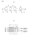
- FIG. 1 The configuration of the laminated band-pass filter in Patent Document 1 is described with reference to Fig. 1 .
- the illustration (A) of Fig. 1 is a circuit diagram thereof, and the illustration (B) of Fig. 1 is a cross-sectional view thereof.
- a plurality of LC parallel resonant circuits are inductively coupled (magnetically coupled).
- Inductors L1, L2, L3, ..., and Ln and capacitors C1, C2, C3, ..., and Cn form a plurality of parallel resonators, and the inductors of neighboring resonators are magnetically coupled.
- a capacitor electrode pattern 12 and an inductor pattern 13 are formed by printing in each of a first layer 10-1, a second layer 10-2, and a third layer 10-3, and these layers form resonators. That is, a capacitor is formed between a ground electrode 11 and the capacitor electrode 12, and the inductor patterns 13 of two layers are electrically connected to each other via a blind through hole 14.
- a plurality of layers forming such resonators are laminated as a fourth layer 10-4 and its underlying layers, thus magnetically coupling neighboring inductors.
- Patent Document 2 describes a laminated band-pass filter in which a plurality of LC resonators is disposed inside a laminated structure of dielectric layers and electrode layers.
- the plurality of LC resonators are made up of a plurality of capacitances formed by a plurality of capacitance forming electrodes and inductances included in the plurality of capacitance forming electrodes.
- the neighboring LC resonators of the LC resonators are disposed inside the laminate structure at different height positions in the thickness direction of the laminated structure and electromagnetically coupled.
- the arrangement in which the plurality of LC resonators are disposed in the laminated structure at different height positions in the thickness directions of the laminated structure can reduce the part size while a physical distance necessary in the design of a band-pass filter is retained between the LC resonators.
- the laminated band-pass filter in Patent Document 3 is the one that includes a filter element in which first and second filter lines each including a pair of parallel lines disposed in part of a wiring layer are opposed to different circuit layers and are electrically connected at one end and the pair of lines is folded through a dielectric layer.
- the laminated band-pass filter in Patent Document 4 is the one in which two strip lines forming a resonator are disposed in the same layer at a specified interval and thereby electromagnetically coupled.
- the inductor included in each of the LC parallel resonators is made up of a two-layer inductor pattern, so a problem arises in which magnetic coupling between the LC parallel resonators is large.
- the inductor made up of the two-layer inductor pattern causes a problem in which a decrease in the Q value of the inductor increases the insertion loss of the laminated band-pass filter.
- the laminated band-pass filter of Patent Document 2 uses self resonance of the capacitor.
- the capacitance component of each of the capacitor electrodes and the inductance component of the capacitor electrode form an LC resonator. Because of this, the resonator cannot have a desired inductance, and characteristics of low insertion loss of the laminated band-pass filter are unobtainable.
- the laminated band-pass filter of each of Patent Documents 3 and 4 can achieve a small size and low insertion loss.
- a multilayer resonator is used to achieve sharp attenuation characteristics from a passband to a range outside the passband, two-stage filters are laminated in the direction of the lamination and strip lines are coupled in the direction of the thickness. This results in a problem in which the multilayer filter has a large thickness.
- an object of the present invention is to solve the above problems and provide a small-sized and loss-loss laminated band-pass filter that has stable passband characteristics having sharp attenuation from a passband to a range outside the passband.
- a laminated band-pass filter includes, as an element assembly, a laminated structure including a plurality of dielectric layers and a plurality of electrode layers, the plurality of electrode layers each having a capacitor electrode and/or an inductor electrode.
- the capacitor electrodes and the inductor electrodes form an even number of LC parallel resonators including neighboring LC parallel resonators being coupled.
- the laminated band-pass filter further includes an input electrode connected to an input-side LC parallel resonator of the even number of LC parallel resonators and an output electrode connected to an output-side LC parallel resonator of the even number of LC parallel resonators.
- the inductor electrode of each of the even number of LC parallel resonators forms a loop starting from a connection between a first end of the inductor electrode and the capacitor electrode.
- the loops formed by the inductor electrodes of at least two of the coupling LC parallel resonators have opposite directions.
- the capacitor electrodes of the even number of LC parallel resonators have a shape and distribution having point symmetry in plan view.
- the inductor electrodes, the input electrode, and the output electrode have a shape and distribution (arrangement) having point symmetry in plan view (when the center of symmetry is a common point in plan), as well as the capacitor electrodes.
- Each of the inductor electrodes is coiled and includes a via electrode disposed in a direction in which the dielectric layers are laminated and a line electrode at least disposed along a direction perpendicular to the direction in which the dielectric layers are laminated.
- the inductor electrodes and the capacitor electrodes are arranged in a direction perpendicular to the direction in which the dielectric layers and the electrode layers are laminated.
- Each of the capacitor electrodes forms a capacitance between the capacitor electrode and a common ground electrode extending over an area where the capacitor electrodes are arranged, and the capacitor electrodes are disposed in the same electrode layer.
- Each of the capacitor electrodes forms a capacitance between the capacitor electrode and a common ground electrode extending over an area where the capacitor electrodes are arranged, and the capacitor electrodes sandwich the ground electrode in a thickness direction and are disposed on opposite sides of the ground electrode.
- each of the inductor electrodes for even number of LC parallel resonators forms the loop and, when viewed from the direction in which the inductor electrodes are arranged, the surfaces of the loops formed by the inductor electrodes of the coupling LC parallel resonators overlap each other at least in part, the degree of coupling (inductive coupling) between neighboring LC parallel resonators can be increased and the pass band can be widened.
- the inductor electrode can be provided separately from the capacitor electrode, the inductor can have a high Q value and the insertion loss can be reduced.
- the resonator does not use self resonance, the resonator can have a desired inductance and a reduction in the insertion loss can be achieved in a desired passband.
- the input and the output have substantially the same impedance characteristics (reflection characteristics), so the passband characteristics of the filter can be stable.
- the laminated band-pass filter can be used as a non-directional band-pass filter.
- the capacitor electrodes are arranged to form capacitance between the common ground electrode extending over the area of the capacitor electrodes, and the neighboring capacitor electrodes produce a capacitance between each other, too.
- a capacitive element for coupling in a LC parallel resonance period which is traditionally required as an independent element, can be omitted, and the Q value of the resonator can be improved. Even if a shift occurs in a layer where a capacitor electrode is disposed during lamination or printing, there is no change in a capacitance between the capacitor electrode and the ground electrode and in a capacitance between the neighboring capacitor electrodes, so variations that would be caused by such a change can be suppressed.
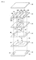
- FIG. 2 is an exploded perspective view of a laminated band-pass filter according to the first embodiment
- Fig. 3 is an external perspective view thereof.
- a ground electrode 109 is disposed on the upper surface of a ground electrode formation layer 103.
- Capacitor electrodes 111 and 114 are disposed in a capacitor electrode formation layer 102.
- Capacitor electrodes 112 and 113 are disposed in a capacitor electrode formation layer 104.
- Input/output electrodes 121 and 122 are disposed in an input/output electrode formation layer 101.
- Line electrodes 116 to 119 are disposed in a line electrode formation layer 105.
- An external layer 106 is disposed above the line electrode formation layer 105.
- the laminated band-pass filter forms a laminated structure including six dielectric layers and five electrode layers and having terminal electrodes disposed on end faces.
- a laminated structure 100 is the above laminated structure including the dielectric layers and electrode layers. Input/output terminals 7 and 8 are disposed on two side surfaces (end faces) opposing each other of four side surfaces of the laminated structure 100, and a ground terminal 6 is disposed on the remaining two side surfaces. In this way, a laminated band-pass filter 1 is configured.
- the laminated structure 100 has a size of 1.6 mm ⁇ 0.8 mm and a height of 0.5 mm.
- LTCC low temperature co-fired ceramics
- a material having a relative dielectric constant in the range from 6 to 80 can be used.
- the electrode layer containing the line electrodes and the dielectric layer laminated thereon, that is, the line electrode formation layer 105 and external layer 106 have a relative dielectric constant in the range from 6 to 80.
- the relative dielectric constant of the capacitor electrode formation layers is equal to or larger than 20.
- Each of the dielectric layers can be, for example, low temperature co-fired ceramics made of a glass component and at least one component of titanium oxide, barium oxide, and alumina.
- the above-described material of which each dielectric layer is made is also applicable to that in another embodiment described below.
- the ground electrode 109 extending over an area slightly smaller than the plane external shape of the ground electrode formation layer 103 and ground connection electrodes 151 and 152 are disposed in the ground electrode formation layer 103.
- the ground connection electrodes 151 and 152 are electrically connected to the ground electrode 109 and extend to two side surfaces of the ground electrode formation layer 103.
- the two ground connection electrodes 151 and 152 are electrically connected to the ground terminal 6, which is illustrated in Fig. 3 .
- the capacitor electrodes 111 and 114 disposed in the capacitor electrode formation layer 102 are substantially rectangular and parallel to each other.
- the capacitor electrodes 112 and 113 disposed in the capacitor electrode formation layer 104 are rectangular and parallel to each other.
- a capacitance is formed between the ground electrode 109 and each of these capacitor electrodes 111 to 114.
- a capacitance is also formed between the neighboring capacitor electrodes.
- the input/output electrodes 121 and 122 disposed in the input/output electrode formation layer 101 are in contact with the two shorter sides thereof and substantially rectangular.
- the two input/output electrodes 121 and 122 are electrically connected to the input/output terminals 7 and 8, respectively, which are illustrated in Fig. 3 .
- the line electrodes 116 to 119 disposed in the line electrode formation layer 105 are parallel to one another and have a linear shape.
- Via electrodes 131 to 138 are disposed in the input/output electrode formation layer 101, the capacitor electrode formation layers 102 and 104, the ground electrode formation layer 103, and the line electrode formation layer 105.
- the via electrodes 131 to 138 extend along the direction of the lamination of these layers.
- the via electrode 131 is electrically connected to a first end 116A of the line electrode 116, the capacitor electrode 111, and the input/output electrode 121.
- the via electrode 132 is electrically connected to a second end 116B of the line electrode 116 and the ground electrode 109.
- the via electrode 133 is electrically connected to a first end 117A of the line electrode 117 and the ground electrode 109.
- the via electrode 134 is electrically connected to a second end 117B of the line electrode 117 and the capacitor electrode 112.
- the via electrode 135 is electrically connected to a first end 118A of the line electrode 118 and the capacitor electrode 113.
- the via electrode 136 is electrically connected to a second end 118B of the line electrode 118 and the ground electrode 109.
- the via electrode 137 is electrically connected to a first end 119A of the line electrode 119 and the ground electrode 109.
- the via electrode 138 is electrically connected to a second end 119B of the line electrode 119, the capacitor electrode 114, and the input/output electrode 122.
- the inductor electrodes made up of the via electrodes and line electrodes and the directions of the loops thereof have a relationship described below.
- a "loop" formed by an inductor electrode is formed by a path of the inductor electrode starting from a connection between a capacitor electrode and the inductor electrode. That is, a loop starts from a connection between a capacitor electrode and a via electrode and is formed by a connection path of the via electrode, a line electrode, and another via electrode.
- a "loop direction” is the direction in which a loop is wound from the starting point of the loop viewed from one direction of the direction in which the line electrodes are arranged.
- a first inductor electrode forms a loop of the connection path from the connection (starting point) between the capacitor electrode 111 and the via electrode 131 to the via electrode 131 to the line electrode 116 to the via electrode 132.
- the loop direction of the first inductor electrode is left-handed.
- a second inductor electrode forms a loop of the connection path from the connection (starting point) between the capacitor electrode 112 and the via electrode 134 to the via electrode 134 to the line electrode 117 to the via electrode 133.
- the loop direction of the second inductor electrode is right-handed.
- a loop can have only two directions of left-handed and right-handed; one direction is represented by "1" and the other is represented by "0.”
- a laminated structure made up of a plurality of dielectric layers and a plurality of electrode layers each including at least one of a capacitor electrode and an inductor electrode, an even number of LC parallel resonators including neighboring LC parallel resonators being coupled using a capacitor electrode and an inductor electrode are configured.
- the polarities of coupling between the four (four-stage) LC parallel resonators shown in Table 1 can be represented as ⁇ 1010> when expressed in sequence from the input side to the output side of the band-pass filter.
- the laminated band-pass filter illustrated in the present embodiment has a characteristic configuration described below.
- the inductor electrodes made up of the via electrodes 131 to 138 extending in the direction in which the dielectric layers are laminated and the line electrodes 116 to 119 extending at least perpendicular to the direction in which the dielectric layers are laminated are coiled.
- the inductor electrodes and capacitor electrodes are arranged perpendicular to the direction in which the dielectric layers and the electrode layers are arranged.
- a capacitance is formed between the common ground electrode 109, which extends over the area where the plurality of capacitor electrodes 111 to 114 are arranged, and each of these capacitor electrodes.
- the capacitor electrodes 111 and 114 are disposed in the same electrode layer, and the capacitor electrodes 112 and 113 are disposed in the same electrode layer.
- Each of the capacitor electrodes is an electrode that forms a capacitance between the electrode and the ground electrode 109, which extends over the area where the plurality of capacitor electrodes 111 to 114 are arranged.
- the capacitor electrodes 111 to 114 sandwich the ground electrode 109 in the direction of the thickness and are disposed on the opposite sides of the ground electrode 109.
- the via electrode 131 connecting to the capacitor electrode 111 and the via electrode 138 connecting to the capacitor electrode 114, the capacitor electrodes 111 and 114 being included in the LC parallel resonators of the input stage and the output stage, are neighboring to the via electrodes 133 and 136, respectively, which are included in the neighboring LC parallel resonators and connect to the ground electrode 109.
- Fig. 4 is an equivalent circuit diagram of the above-described laminated band-pass filter.
- an input terminal IN corresponds to the input/output terminal 7, which is illustrated in Fig. 3 and electrically connected to the input/output electrode 121 illustrated in Fig. 2
- an output terminal OUT corresponds to the input/output terminal 8, which is electrically connected to the input/output electrode 122.
- An inductor L1 is the one in which an inductance produced by the inductor electrode made up of the via electrodes 131 and 132 and the line electrode 116 is symbolized.
- An inductor L2 is the one in which an inductance produced by the inductor electrode made up of the via electrodes 133 and 134 and the line electrode 117 is symbolized.
- an inductor L3 is the one in which an inductance produced by the inductor electrode made up of the via electrodes 135 and 136 and the line electrode 118 is symbolized.
- An inductor L4 is the one in which an inductance produced by the inductor electrode made up of the via electrodes 137 and 138 and the line electrode 119 is symbolized.
- Capacitors C1 to C4 are the ones in which capacitances occurring between the capacitor electrodes 111 to 114 and the ground electrode 109 are symbolized.
- a capacitor C23 is the one in which a parasitic capacitance occurring between the capacitor electrodes 112 and 113 is symbolized and contributes to the capacitive coupling between the second-stage and third-stage LC parallel resonators.
- a capacitor C14 is the one in which a parasitic capacitance occurring between the capacitor electrodes 111 and 114 is symbolized and contributes to the jump coupling between the first-stage and fourth-stage LC parallel resonators.
- the loop surfaces formed by the inductor electrodes each made up of two via electrodes and one line electrode overlap each other at least in part.
- at least inductors formed by neighboring inductor electrodes are inductively coupled to each other.
- M1 represents an inductive coupling formed by the inductors L1 and L2
- M2 represents an inductive coupling formed by the inductors L2 and L3
- M3 represents an inductive coupling formed by the inductors L3 and L4.
- Fig. 5 illustrates passband characteristics (S21 characteristics for S parameter) and reflection characteristics (S11 characteristics and S22 characteristics for S parameter) of the above-described laminated band-pass filter.
- the band-pass filter characteristics of allowing the passage in the frequency band from 3.3 to 4.0 GHz and blocking the passage in the other frequency bands are obtainable.
- an attenuation pole occurs. A large amount of the attenuation in the vicinity of the attenuation pole is achieved.
- the attenuation pole is caused by inductive coupling of an even number of LC parallel resonators in opposite polarities in an alternating manner.
- the reflection characteristic S11 of the input/output terminal 7 and the reflection characteristic S12 of the input/output terminal 8 are substantially the same. Thus, there are few ripples, and the obtained characteristic is stable. In addition, there is not much difference between the impedance characteristic (reflection characteristic) of the input and those of the output, so the laminated band-pass filter can be used as a band-pass filter having non-directional input/output terminals.
- LC parallel resonators including U-shaped inductors rotated 90° made by the via electrodes and line electrodes are arranged transversely. Accordingly, the low-loss passband characteristic is obtainable.
- capacitor electrodes 111 and 114 and the capacitor electrodes 112 and 113 are separately disposed in the opposite layers sandwiching the ground electrode 109, coupling produced by an unnecessary capacitance component between predetermined neighboring LC parallel resonators (capacitive coupling between the first and second stages and capacitive coupling between the third and fourth stages) can be suppressed. Because the capacitor electrodes (111, 114) for jump coupling can be disposed in a single layer, even if there is a shift in printing or laminating, the laminated structure is not affected by the shift and variations in capacitance for jump coupling can be suppressed.
- the laminated structure is not affected by the shift, and this results in reduced variations in resonant frequency. Also for the capacitor electrodes 111 and 114, which are connected to the input/output electrodes 121 and 122, respectively, because they are connected in different layers through the via electrodes 131 and 138, even if there is a shift in printing or laminating, the laminated structure is not affected by the shift. Accordingly, variations in capacitance can be suppressed.
- FIG. 6 is an exploded perspective view of the laminated band-pass filter according to the second embodiment.
- a ground electrode 209 is disposed on the upper surface of a ground electrode formation layer 201.
- Capacitor electrodes 211, 212, 213, and 214 are disposed in a capacitor electrode formation layer 202.
- Input/output electrodes 221 and 222 are disposed in an input/output electrode formation layer 203.
- Line electrodes 216 to 219 are disposed in a line electrode formation layer 204.
- An external layer 205 is disposed above the line electrode formation layer 204.
- the laminated band-pass filter forms a laminated structure including five dielectric layers and four electrode layers and having terminal electrodes disposed on end faces.
- the material of the dielectric layer portion of each layer is substantially the same as in the first embodiment.
- the appearance of the laminated band-pass filter is substantially the same as that illustrated in Fig. 3 .
- the ground electrode 209 extending over an area slightly smaller than the plane external shape of the ground electrode formation layer 201 and ground connection electrodes 251 and 252 are disposed in the ground electrode formation layer 201.
- the ground connection electrodes 251 and 252 are electrically connected to the ground electrode 209 and extend to two side surfaces of the ground electrode formation layer 201.
- the two ground connection electrodes 251 and 252 are electrically connected to a ground terminal disposed on side surfaces of the laminated structure.
- the four capacitor electrodes 211 to 214 disposed in the capacitor electrode formation layer 202 are rectangular and parallel to one another. A capacitance is formed between the ground electrode 209 and each of these capacitor electrodes 211 to 214. A capacitance is also formed between the neighboring capacitor electrodes.
- the input/output electrodes 221 and 222 disposed in the input/output electrode formation layer 203 are in contact with the two shorter sides thereof and substantially rectangular.
- the two input/output electrodes 221 and 222 are electrically connected to input/output terminals of the laminated structure.
- the line electrodes 216 to 219 disposed in the line electrode formation layer 204 are parallel to one another and have a linear shape.
- Via electrodes 231 to 238 are disposed in the input/output electrode formation layer 203, the capacitor electrode formation layer 202, the ground electrode formation layer 201, and the line electrode formation layer 204.
- the via electrodes 231 to 238 extend along the direction of the lamination of these layers.
- the via electrode 231 is electrically connected to a first end 216A of the line electrode 216, the capacitor electrode 211, and the input/output electrode 221.
- the via electrode 232 is electrically connected to a second end 216B of the line electrode 216 and the ground electrode 209.
- the via electrode 233 is electrically connected to a first end 217A of the line electrode 217 and the ground electrode 209.
- the via electrode 234 is electrically connected to a second end 217B of the line electrode 217 and the capacitor electrode 212.
- the via electrode 235 is electrically connected to a first end 218A of the line electrode 218 and the capacitor electrode 213.
- the via electrode 236 is electrically connected to a second end 218B of the line electrode 218 and the ground electrode 209.
- the via electrode 237 is electrically connected to a first end 219A of the line electrode 219 and the ground electrode 209.
- the via electrode 238 is electrically connected to a second end 219B of the line electrode 219, the capacitor electrode 214, and the input/output electrode 222.
- the inductor electrodes formed by the via electrodes and line electrodes and the directions of the loops thereof have a relationship described below.
- a "loop" formed by an inductor electrode is formed by a path of the inductor electrode starting from a connection between a capacitor electrode and the inductor electrode, as in the case of the first embodiment. That is, a loop starts from a connection between a capacitor electrode and a via electrode and is formed by a connection path of the via electrode, a line electrode, and another via electrode.
- the four capacitor electrodes 211 to 214 are disposed in the single layer 202, and a capacitance is formed between neighboring capacitor electrodes.
- Fig. 7 is an equivalent circuit diagram of the above-described laminated band-pass filter.
- an inductor L1 is the one in which an inductance produced by the inductor electrode made up of the via electrodes 231 and 232 and the line electrode 216 is symbolized.
- An inductor L2 is the one in which an inductance produced by the inductor electrode made up of the via electrodes 233 and 234 and the line electrode 217 is symbolized.
- an inductor L3 is the one in which an inductance produced by the inductor electrode made up of the via electrodes 235 and 236 and the line electrode 218 is symbolized.
- An inductor L4 is the one in which an inductance produced by the inductor electrode made up of the via electrodes 237 and 238 and the line electrode 219 is symbolized.
- Capacitors C1 to C4 are the ones in which capacitances formed between the capacitor electrodes 211 to 214 and the ground electrode 209 are symbolized.
- a capacitor C12 is the one in which a parasitic capacitance formed between the capacitor electrodes 211 and 212 is symbolized.
- a capacitor C23 is the one in which a parasitic capacitance formed between the capacitor electrodes 212 and 213 is symbolized.
- a capacitor C34 is the one in which a parasitic capacitance formed between the capacitor electrodes 213 and 214 is symbolized.
- the loop surfaces formed by the inductor electrodes each made up of two via electrodes and one line electrode overlap each other at least in part.
- at least inductors formed by neighboring inductor electrodes are inductively coupled to each other.
- M1 represents an inductive coupling formed by the inductors L1 and L2
- M2 represents an inductive coupling formed by the inductors L2 and L3
- M3 represents an inductive coupling formed by the inductors L3 and L4.
- the ground electrode 209 can have a flat-type electrode structure, and the capacitor electrodes 211 to 214 can be disposed in the same layer. Accordingly, capacitance formed by a shift in laminating and variations in parasitic capacitance between the capacitor electrodes can be suppressed, and non-uniformity of electric characteristics are reduced structurally.
- the line electrodes 216 to 219, the capacitor electrodes 211 to 214, and the ground electrode 209 are connected with the via electrodes 231 to 238, and the input/output electrodes 221 and 222, which connect to the input/output terminals, are arranged between the line electrode formation layer 204 and the capacitor electrode formation layer 202.
- This configuration enables the LC parallel resonators to be constructed using a closed loop and achieves the band-pass filter while maintaining high Q resonator characteristics.
Landscapes
- Physics & Mathematics (AREA)
- Electromagnetism (AREA)
- Filters And Equalizers (AREA)
- Coils Or Transformers For Communication (AREA)
Abstract
Description
- The present invention relates to a laminated band-pass filter in which a plurality of dielectric layers and electrode layers are laminated.
- A traditional high-frequency band-pass filter suited for reducing its size and cost is one in which a plurality of LC resonators is disposed in a laminated structure of dielectric layers and electrode layers. Examples of such a laminated band-pass filter are disclosed in Patent Documents 1 to 4.
- The configuration of the laminated band-pass filter in Patent Document 1 is described with reference to
Fig. 1 . The illustration (A) ofFig. 1 is a circuit diagram thereof, and the illustration (B) ofFig. 1 is a cross-sectional view thereof. In the filter, a plurality of LC parallel resonant circuits are inductively coupled (magnetically coupled). Inductors L1, L2, L3, ..., and Ln and capacitors C1, C2, C3, ..., and Cn form a plurality of parallel resonators, and the inductors of neighboring resonators are magnetically coupled. - As illustrated in (B) of
Fig. 1 , acapacitor electrode pattern 12 and aninductor pattern 13 are formed by printing in each of a first layer 10-1, a second layer 10-2, and a third layer 10-3, and these layers form resonators. That is, a capacitor is formed between aground electrode 11 and thecapacitor electrode 12, and theinductor patterns 13 of two layers are electrically connected to each other via a blind throughhole 14. A plurality of layers forming such resonators are laminated as a fourth layer 10-4 and its underlying layers, thus magnetically coupling neighboring inductors. - Patent Document 2 describes a laminated band-pass filter in which a plurality of LC resonators is disposed inside a laminated structure of dielectric layers and electrode layers. The plurality of LC resonators are made up of a plurality of capacitances formed by a plurality of capacitance forming electrodes and inductances included in the plurality of capacitance forming electrodes. The neighboring LC resonators of the LC resonators are disposed inside the laminate structure at different height positions in the thickness direction of the laminated structure and electromagnetically coupled. The arrangement in which the plurality of LC resonators are disposed in the laminated structure at different height positions in the thickness directions of the laminated structure can reduce the part size while a physical distance necessary in the design of a band-pass filter is retained between the LC resonators.
- The laminated band-pass filter in Patent Document 3 is the one that includes a filter element in which first and second filter lines each including a pair of parallel lines disposed in part of a wiring layer are opposed to different circuit layers and are electrically connected at one end and the pair of lines is folded through a dielectric layer.
- The laminated band-pass filter in Patent Document 4 is the one in which two strip lines forming a resonator are disposed in the same layer at a specified interval and thereby electromagnetically coupled.
- [Patent Document 1] Japanese Unexamined Patent Application Publication No.
4-6911 - [Patent Document 2] Japanese Unexamined Patent Application Publication No.
2000-201001 - [Patent Document 3] Japanese Unexamined Patent Application Publication No.
2003-198226 - [Patent Document 4] International Publication No.
WO 02/009225 - For the laminated band-pass filter of Patent Document 1, the inductor included in each of the LC parallel resonators is made up of a two-layer inductor pattern, so a problem arises in which magnetic coupling between the LC parallel resonators is large. The inductor made up of the two-layer inductor pattern causes a problem in which a decrease in the Q value of the inductor increases the insertion loss of the laminated band-pass filter. To solve the above problems, it is necessary to have a sufficiently long distance between the LC parallel resonators. This results in a problem in which the thickness of the laminated band-pass filter is large.
- The laminated band-pass filter of Patent Document 2 uses self resonance of the capacitor. The capacitance component of each of the capacitor electrodes and the inductance component of the capacitor electrode form an LC resonator. Because of this, the resonator cannot have a desired inductance, and characteristics of low insertion loss of the laminated band-pass filter are unobtainable.
- The laminated band-pass filter of each of Patent Documents 3 and 4 can achieve a small size and low insertion loss. However, if a multilayer resonator is used to achieve sharp attenuation characteristics from a passband to a range outside the passband, two-stage filters are laminated in the direction of the lamination and strip lines are coupled in the direction of the thickness. This results in a problem in which the multilayer filter has a large thickness.
- For these traditional laminated band-pass filters, when an LC parallel resonator made up of a capacitor electrode and an inductor electrode is arranged in a laminated structure and neighboring inductor electrodes are inductively coupled, there is a problem in which a ripple (deviation) occurs in passband characteristics.
- Accordingly, it is an object of the present invention is to solve the above problems and provide a small-sized and loss-loss laminated band-pass filter that has stable passband characteristics having sharp attenuation from a passband to a range outside the passband.
- (1) A laminated band-pass filter includes, as an element assembly, a laminated structure including a plurality of dielectric layers and a plurality of electrode layers, the plurality of electrode layers each having a capacitor electrode and/or an inductor electrode. The capacitor electrodes and the inductor electrodes form an even number of LC parallel resonators including neighboring LC parallel resonators being coupled. The laminated band-pass filter further includes an input electrode connected to an input-side LC parallel resonator of the even number of LC parallel resonators and an output electrode connected to an output-side LC parallel resonator of the even number of LC parallel resonators. The inductor electrode of each of the even number of LC parallel resonators forms a loop starting from a connection between a first end of the inductor electrode and the capacitor electrode. When viewed in a direction in which the inductor electrodes are arranged, surfaces of the loops formed by the inductor electrodes of coupling LC parallel resonators of the LC parallel resonators overlap each other at least in part. When viewed in the direction in which the inductor electrodes are arranged, the loops formed by the inductor electrodes of at least two of the coupling LC parallel resonators have opposite directions. The capacitor electrodes of the even number of LC parallel resonators have a shape and distribution having point symmetry in plan view.
- (2) The inductor electrodes, the input electrode, and the output electrode have a shape and distribution (arrangement) having point symmetry in plan view (when the center of symmetry is a common point in plan), as well as the capacitor electrodes.
- (3) The loops formed by the inductor electrodes of the neighboring LC parallel resonators have opposite directions.
- (4) Each of the inductor electrodes is coiled and includes a via electrode disposed in a direction in which the dielectric layers are laminated and a line electrode at least disposed along a direction perpendicular to the direction in which the dielectric layers are laminated. The inductor electrodes and the capacitor electrodes are arranged in a direction perpendicular to the direction in which the dielectric layers and the electrode layers are laminated.
- (5) Each of the capacitor electrodes forms a capacitance between the capacitor electrode and a common ground electrode extending over an area where the capacitor electrodes are arranged, and the capacitor electrodes are disposed in the same electrode layer.
- (6) Each of the capacitor electrodes forms a capacitance between the capacitor electrode and a common ground electrode extending over an area where the capacitor electrodes are arranged, and the capacitor electrodes sandwich the ground electrode in a thickness direction and are disposed on opposite sides of the ground electrode. Advantages
- With the present invention, the following advantages are achievable.
(1) Because each of the inductor electrodes for even number of LC parallel resonators forms the loop and, when viewed from the direction in which the inductor electrodes are arranged, the surfaces of the loops formed by the inductor electrodes of the coupling LC parallel resonators overlap each other at least in part, the degree of coupling (inductive coupling) between neighboring LC parallel resonators can be increased and the pass band can be widened. - Because the inductor electrode can be provided separately from the capacitor electrode, the inductor can have a high Q value and the insertion loss can be reduced.
- Because the resonator does not use self resonance, the resonator can have a desired inductance and a reduction in the insertion loss can be achieved in a desired passband.
- Because the loops formed by the inductor electrodes of neighboring LC parallel resonators have opposite directions, a ripple of insertion loss in passband can be suppressed and satisfactory passband characteristics are obtainable.
- In addition, the input and the output have substantially the same impedance characteristics (reflection characteristics), so the passband characteristics of the filter can be stable.
- (2) The configuration in which the inductor electrodes, the input electrode, and the output electrode have a shape and distribution (arrangement) having point symmetry in plan view, as well as the capacitor electrodes, further facilitates the sameness of the impedance characteristics (reflection characteristics) of the input and that of the output. Accordingly, the laminated band-pass filter can be used as a non-directional band-pass filter.
- (3) The relationship of the opposite directions of the loops formed by the inductor electrodes of neighboring LC parallel resonators enables a design in which an attenuation pole is present in bands lower and higher than the passband. This eliminates the necessity of a capacitor between input and output to design a sufficient amount of attenuation in lower bands. Accordingly, there is no need to have a structure in which capacitor electrodes for forming input/output resonators are neighboring and a structure in which an electrode connecting between input and output capacitors is disposed, and thus variations in characteristics resulting from the accuracy of forming these electrode patterns do not occur. Accordingly, a stable characterized band-pass filter having high attenuation characteristics is obtainable.
- (4) The arrangement in which the inductor electrodes and the capacitor electrodes of the LC parallel resonators are arranged in a direction perpendicular to the direction in which the dielectric layers and the electrode layers are laminated can make the gap between the surfaces of the loops formed by neighboring inductor electrodes constant. Accordingly, even if a shift occurs in a surface direction of each of the dielectric layers and the electrode layers during lamination, the shift between the inductor electrodes of neighboring LC parallel resonators can be virtually eliminated. Thus, the band-pass filter characteristics whose variations are reduced are obtainable.
- (5) In the LC parallel resonator, the capacitor electrodes are arranged to form capacitance between the common ground electrode extending over the area of the capacitor electrodes, and the neighboring capacitor electrodes produce a capacitance between each other, too. Thus, a capacitive element for coupling in a LC parallel resonance period, which is traditionally required as an independent element, can be omitted, and the Q value of the resonator can be improved. Even if a shift occurs in a layer where a capacitor electrode is disposed during lamination or printing, there is no change in a capacitance between the capacitor electrode and the ground electrode and in a capacitance between the neighboring capacitor electrodes, so variations that would be caused by such a change can be suppressed.
- (6) Arranging the capacitor electrodes of the LC parallel resonators so as to sandwich the ground electrode in the thickness direction and be disposed on opposite sides of the ground electrode enables a capacitor for coupling between neighboring LC parallel resonators and a capacitor for jump coupling between distant LC parallel resonators to be disposed in a limited area, and this results in a reduction in the whole size.
-
- [
Fig. 1] Fig. 1 is an equivalent circuit diagram and a cross-sectional view of a laminated band-pass filter illustrated in Patent Document 1. - [
Fig. 2] Fig. 2 is an exploded perspective view of a laminated band-pass filter according to a first embodiment. - [
Fig. 3] Fig. 3 is an external perspective view of the laminated band-pass filter. - [
Fig. 4] Fig. 4 is an equivalent circuit diagram of the laminated band-pass filter. - [
Fig. 5] Fig. 5 illustrates passband characteristics and reflection characteristics of the laminated band-pass filter. - [
Fig. 6] Fig. 6 is an exploded perspective view of a laminated band-pass filter according to a second embodiment. - [
Fig. 7] Fig. 7 is an equivalent circuit diagram of the laminated band-pass filter. -
- 1
- laminated band-pass filter
- 6
- ground terminal
- 7, 8
- input/output terminal
- 100
- laminated structure
- 101, 203
- input/output electrode formation layer
- 102, 104, 202
- capacitor electrode formation layer
- 103, 201
- ground electrode formation layer
- 105, 204
- line electrode formation layer
- 106, 205
- external layer
- 109, 209
- ground electrode
- 111-114, 211-214
- capacitor electrode
- 116-119, 216-219
- line electrode
- 121, 122, 221, 222
- input/output electrode
- 131-138, 231-238
- via electrode
- 151, 152, 251, 252
- ground connection electrode
- L1-L5
- inductor
- C1-C5
- capacitor
- C12, C23, C34, C14
- capacitance
- M1-M4
- inductive coupling
- A laminated band-pass filter according to a first embodiment is described with reference to
Figs. 2-5 .
Fig. 2 is an exploded perspective view of a laminated band-pass filter according to the first embodiment, andFig. 3 is an external perspective view thereof. - In
Fig. 2 , aground electrode 109 is disposed on the upper surface of a groundelectrode formation layer 103.Capacitor electrodes electrode formation layer 102.Capacitor electrodes electrode formation layer 104. Input/output electrodes electrode formation layer 101.Line electrodes 116 to 119 are disposed in a lineelectrode formation layer 105. Anexternal layer 106 is disposed above the lineelectrode formation layer 105. The laminated band-pass filter forms a laminated structure including six dielectric layers and five electrode layers and having terminal electrodes disposed on end faces. - In
Fig. 3 , alaminated structure 100 is the above laminated structure including the dielectric layers and electrode layers. Input/output terminals 7 and 8 are disposed on two side surfaces (end faces) opposing each other of four side surfaces of thelaminated structure 100, and a ground terminal 6 is disposed on the remaining two side surfaces. In this way, a laminated band-pass filter 1 is configured. Thelaminated structure 100 has a size of 1.6 mm × 0.8 mm and a height of 0.5 mm. - The dielectric-layer portion of each layer is low temperature co-fired ceramics (LTCC) having a relative dielectric constant sr = 53.5. As the dielectric layer, a material having a relative dielectric constant in the range from 6 to 80 can be used.
- The electrode layer containing the line electrodes and the dielectric layer laminated thereon, that is, the line
electrode formation layer 105 andexternal layer 106 have a relative dielectric constant in the range from 6 to 80. The relative dielectric constant of the capacitor electrode formation layers is equal to or larger than 20. Each of the dielectric layers can be, for example, low temperature co-fired ceramics made of a glass component and at least one component of titanium oxide, barium oxide, and alumina. The above-described material of which each dielectric layer is made is also applicable to that in another embodiment described below. - In
Fig. 2 , theground electrode 109 extending over an area slightly smaller than the plane external shape of the groundelectrode formation layer 103 andground connection electrodes electrode formation layer 103. Theground connection electrodes ground electrode 109 and extend to two side surfaces of the groundelectrode formation layer 103. The twoground connection electrodes Fig. 3 . - The
capacitor electrodes electrode formation layer 102 are substantially rectangular and parallel to each other. Thecapacitor electrodes electrode formation layer 104 are rectangular and parallel to each other. A capacitance is formed between theground electrode 109 and each of thesecapacitor electrodes 111 to 114. A capacitance is also formed between the neighboring capacitor electrodes. - The input/
output electrodes electrode formation layer 101 are in contact with the two shorter sides thereof and substantially rectangular. The two input/output electrodes Fig. 3 . - The
line electrodes 116 to 119 disposed in the lineelectrode formation layer 105 are parallel to one another and have a linear shape. - Via
electrodes 131 to 138 are disposed in the input/outputelectrode formation layer 101, the capacitor electrode formation layers 102 and 104, the groundelectrode formation layer 103, and the lineelectrode formation layer 105. The viaelectrodes 131 to 138 extend along the direction of the lamination of these layers. The viaelectrode 131 is electrically connected to afirst end 116A of theline electrode 116, thecapacitor electrode 111, and the input/output electrode 121. The viaelectrode 132 is electrically connected to asecond end 116B of theline electrode 116 and theground electrode 109. The viaelectrode 133 is electrically connected to afirst end 117A of theline electrode 117 and theground electrode 109. The viaelectrode 134 is electrically connected to asecond end 117B of theline electrode 117 and thecapacitor electrode 112. The viaelectrode 135 is electrically connected to afirst end 118A of theline electrode 118 and thecapacitor electrode 113. The viaelectrode 136 is electrically connected to asecond end 118B of theline electrode 118 and theground electrode 109. The viaelectrode 137 is electrically connected to afirst end 119A of theline electrode 119 and theground electrode 109. The viaelectrode 138 is electrically connected to asecond end 119B of theline electrode 119, thecapacitor electrode 114, and the input/output electrode 122. - Accordingly, the inductor electrodes made up of the via electrodes and line electrodes and the directions of the loops thereof have a relationship described below.
-
[Table 1] Inductor Electrode Via Electrode Line electrode Loop Direction First 131, 132 116 1 Second 133, 134 117 0 Third 135, 136 118 1 Fourth 137, 138 119 0 - A "loop direction" is the direction in which a loop is wound from the starting point of the loop viewed from one direction of the direction in which the line electrodes are arranged. For example, when, in
Fig. 2 , the loops formed by the inductor electrodes are viewed from the input/output electrode 121 toward the input/output electrode 122, a first inductor electrode forms a loop of the connection path from the connection (starting point) between thecapacitor electrode 111 and the viaelectrode 131 to the viaelectrode 131 to theline electrode 116 to the viaelectrode 132. The loop direction of the first inductor electrode is left-handed. A second inductor electrode forms a loop of the connection path from the connection (starting point) between thecapacitor electrode 112 and the viaelectrode 134 to the viaelectrode 134 to theline electrode 117 to the viaelectrode 133. The loop direction of the second inductor electrode is right-handed. Here, a loop can have only two directions of left-handed and right-handed; one direction is represented by "1" and the other is represented by "0." - In such a way, in a laminated structure made up of a plurality of dielectric layers and a plurality of electrode layers each including at least one of a capacitor electrode and an inductor electrode, an even number of LC parallel resonators including neighboring LC parallel resonators being coupled using a capacitor electrode and an inductor electrode are configured.
- The polarities of coupling between the four (four-stage) LC parallel resonators shown in Table 1 can be represented as <1010> when expressed in sequence from the input side to the output side of the band-pass filter.
- As described above, the laminated band-pass filter illustrated in the present embodiment has a characteristic configuration described below.
- (1) The shape and distribution (arrangement) of the
capacitor electrodes 111 to 114 of an even number of LC parallel resonators have point symmetry in plan view. - (2) The shape and distribution (arrangement) of the inductor electrodes made up of the via
electrodes 131 to 138 and theline electrodes 116 to 119 and the input/output electrodes capacitor electrodes 111 to 114, have point symmetry in plan view with respect to the center of the dielectric layer. - (3) The inductor electrodes of neighboring LC parallel resonators have opposite loop directions.
- (4) In the inductor electrodes, the inductor electrodes made up of the via
electrodes 131 to 138 extending in the direction in which the dielectric layers are laminated and theline electrodes 116 to 119 extending at least perpendicular to the direction in which the dielectric layers are laminated are coiled. The inductor electrodes and capacitor electrodes are arranged perpendicular to the direction in which the dielectric layers and the electrode layers are arranged. - (5) A capacitance is formed between the
common ground electrode 109, which extends over the area where the plurality ofcapacitor electrodes 111 to 114 are arranged, and each of these capacitor electrodes. Thecapacitor electrodes capacitor electrodes - (6) Each of the capacitor electrodes is an electrode that forms a capacitance between the electrode and the
ground electrode 109, which extends over the area where the plurality ofcapacitor electrodes 111 to 114 are arranged. Thecapacitor electrodes 111 to 114 sandwich theground electrode 109 in the direction of the thickness and are disposed on the opposite sides of theground electrode 109. - (7) The via
electrode 131 connecting to thecapacitor electrode 111 and the viaelectrode 138 connecting to thecapacitor electrode 114, thecapacitor electrodes electrodes ground electrode 109. -
Fig. 4 is an equivalent circuit diagram of the above-described laminated band-pass filter.
InFig. 4 , an input terminal IN corresponds to the input/output terminal 7, which is illustrated inFig. 3 and electrically connected to the input/output electrode 121 illustrated inFig. 2 , and an output terminal OUT corresponds to the input/output terminal 8, which is electrically connected to the input/output electrode 122. An inductor L1 is the one in which an inductance produced by the inductor electrode made up of the viaelectrodes line electrode 116 is symbolized. An inductor L2 is the one in which an inductance produced by the inductor electrode made up of the viaelectrodes line electrode 117 is symbolized. Similarly, an inductor L3 is the one in which an inductance produced by the inductor electrode made up of the viaelectrodes line electrode 118 is symbolized. An inductor L4 is the one in which an inductance produced by the inductor electrode made up of the viaelectrodes line electrode 119 is symbolized. - Capacitors C1 to C4 are the ones in which capacitances occurring between the
capacitor electrodes 111 to 114 and theground electrode 109 are symbolized. A capacitor C23 is the one in which a parasitic capacitance occurring between thecapacitor electrodes capacitor electrodes - When viewed from the direction of the arrangement of the inductor electrodes, the loop surfaces formed by the inductor electrodes each made up of two via electrodes and one line electrode overlap each other at least in part. Thus, at least inductors formed by neighboring inductor electrodes are inductively coupled to each other.
- In
Fig. 4 , M1 represents an inductive coupling formed by the inductors L1 and L2, M2 represents an inductive coupling formed by the inductors L2 and L3, and M3 represents an inductive coupling formed by the inductors L3 and L4. -
Fig. 5 illustrates passband characteristics (S21 characteristics for S parameter) and reflection characteristics (S11 characteristics and S22 characteristics for S parameter) of the above-described laminated band-pass filter.
As illustrated inFig. 5 , in this example, the band-pass filter characteristics of allowing the passage in the frequency band from 3.3 to 4.0 GHz and blocking the passage in the other frequency bands are obtainable. At 2.2 GHz and 4.5 GHz, an attenuation pole occurs. A large amount of the attenuation in the vicinity of the attenuation pole is achieved. The attenuation pole is caused by inductive coupling of an even number of LC parallel resonators in opposite polarities in an alternating manner. - The reflection characteristic S11 of the input/output terminal 7 and the reflection characteristic S12 of the input/output terminal 8 are substantially the same. Thus, there are few ripples, and the obtained characteristic is stable. In addition, there is not much difference between the impedance characteristic (reflection characteristic) of the input and those of the output, so the laminated band-pass filter can be used as a band-pass filter having non-directional input/output terminals.
- With the first embodiment, unlike traditional laminated band-pass filters, LC parallel resonators including U-shaped inductors rotated 90° made by the via electrodes and line electrodes are arranged transversely. Accordingly, the low-loss passband characteristic is obtainable.
- The arrangement in which the via
electrode 131 connecting to thecapacitor electrode 111 and the viaelectrode 138 connecting to thecapacitor electrode 114, thecapacitor electrodes electrodes ground electrode 109, enables optimal electromagnetic coupling and can achieve a small size and low profile of the laminated structure. Because thecapacitor electrodes capacitor electrodes ground electrode 109, coupling produced by an unnecessary capacitance component between predetermined neighboring LC parallel resonators (capacitive coupling between the first and second stages and capacitive coupling between the third and fourth stages) can be suppressed. Because the capacitor electrodes (111, 114) for jump coupling can be disposed in a single layer, even if there is a shift in printing or laminating, the laminated structure is not affected by the shift and variations in capacitance for jump coupling can be suppressed. - Because of the configuration in which the
line electrodes 116 to 119, thecapacitor electrodes 111 to 114, and theground electrode 109 are connected with the viaelectrodes 131 to 138, even if there is a shift in cutting or laminating dielectric sheets, the laminated structure is not affected by the shift, and this results in reduced variations in resonant frequency. Also for thecapacitor electrodes output electrodes electrodes - In addition, because of a designed point symmetric configuration, impedance characteristics from input and output are substantially the same. Therefore, stable passband characteristics are obtainable.
- The configuration in which all of the loop directions of the inductor electrodes of neighboring LC parallel resonators have opposite <1010> relationship allows an attenuation pole to be designed in both of lower and higher bands than the passband in design. This eliminates the necessity of a capacitor for coupling between input and output to achieve a necessary amount of attenuation in lower bands. Accordingly, variations in parasitic capacitance between capacitor electrodes can be suppressed, and a stable characterized band-pass filter having high attenuation characteristics is obtainable.
- A laminated band-pass filter according to a second embodiment is described with reference to
Figs. 6 and 7. Fig. 6 is an exploded perspective view of the laminated band-pass filter according to the second embodiment. - In
Fig. 6 , aground electrode 209 is disposed on the upper surface of a groundelectrode formation layer 201.Capacitor electrodes electrode formation layer 202. Input/output electrodes electrode formation layer 203.Line electrodes 216 to 219 are disposed in a lineelectrode formation layer 204. Anexternal layer 205 is disposed above the lineelectrode formation layer 204. The laminated band-pass filter forms a laminated structure including five dielectric layers and four electrode layers and having terminal electrodes disposed on end faces. - The material of the dielectric layer portion of each layer is substantially the same as in the first embodiment. The appearance of the laminated band-pass filter is substantially the same as that illustrated in
Fig. 3 . - In
Fig. 6 , theground electrode 209 extending over an area slightly smaller than the plane external shape of the groundelectrode formation layer 201 andground connection electrodes electrode formation layer 201. Theground connection electrodes ground electrode 209 and extend to two side surfaces of the groundelectrode formation layer 201. The twoground connection electrodes - The four
capacitor electrodes 211 to 214 disposed in the capacitorelectrode formation layer 202 are rectangular and parallel to one another. A capacitance is formed between theground electrode 209 and each of thesecapacitor electrodes 211 to 214. A capacitance is also formed between the neighboring capacitor electrodes. - The input/
output electrodes electrode formation layer 203 are in contact with the two shorter sides thereof and substantially rectangular. The two input/output electrodes - The
line electrodes 216 to 219 disposed in the lineelectrode formation layer 204 are parallel to one another and have a linear shape. - Via
electrodes 231 to 238 are disposed in the input/outputelectrode formation layer 203, the capacitorelectrode formation layer 202, the groundelectrode formation layer 201, and the lineelectrode formation layer 204. The viaelectrodes 231 to 238 extend along the direction of the lamination of these layers. The viaelectrode 231 is electrically connected to afirst end 216A of theline electrode 216, thecapacitor electrode 211, and the input/output electrode 221. The viaelectrode 232 is electrically connected to asecond end 216B of theline electrode 216 and theground electrode 209. The via electrode 233 is electrically connected to afirst end 217A of theline electrode 217 and theground electrode 209. The viaelectrode 234 is electrically connected to asecond end 217B of theline electrode 217 and thecapacitor electrode 212. The via electrode 235 is electrically connected to a first end 218A of theline electrode 218 and thecapacitor electrode 213. The viaelectrode 236 is electrically connected to asecond end 218B of theline electrode 218 and theground electrode 209. The viaelectrode 237 is electrically connected to afirst end 219A of theline electrode 219 and theground electrode 209. The viaelectrode 238 is electrically connected to asecond end 219B of theline electrode 219, thecapacitor electrode 214, and the input/output electrode 222. - Accordingly, the inductor electrodes formed by the via electrodes and line electrodes and the directions of the loops thereof have a relationship described below.
-
[Table 2] Inductor Electrode Via Electrode Line electrode Loop Direction First 231,232 216 1 Second 233,234 217 0 Third 235,236 218 1 Fourth 237,238 219 0 - Unlike the first embodiment, in the example illustrated in
Fig. 6 , the fourcapacitor electrodes 211 to 214 are disposed in thesingle layer 202, and a capacitance is formed between neighboring capacitor electrodes. -
Fig. 7 is an equivalent circuit diagram of the above-described laminated band-pass filter.
InFig. 7 , an inductor L1 is the one in which an inductance produced by the inductor electrode made up of the viaelectrodes line electrode 216 is symbolized. An inductor L2 is the one in which an inductance produced by the inductor electrode made up of the viaelectrodes 233 and 234 and theline electrode 217 is symbolized. Similarly, an inductor L3 is the one in which an inductance produced by the inductor electrode made up of the viaelectrodes 235 and 236 and theline electrode 218 is symbolized. An inductor L4 is the one in which an inductance produced by the inductor electrode made up of the viaelectrodes line electrode 219 is symbolized. - Capacitors C1 to C4 are the ones in which capacitances formed between the
capacitor electrodes 211 to 214 and theground electrode 209 are symbolized. A capacitor C12 is the one in which a parasitic capacitance formed between thecapacitor electrodes capacitor electrodes capacitor electrodes - When viewed from the direction of the arrangement of the inductor electrodes, the loop surfaces formed by the inductor electrodes each made up of two via electrodes and one line electrode overlap each other at least in part. Thus, at least inductors formed by neighboring inductor electrodes are inductively coupled to each other.
- In
Fig. 7 , M1 represents an inductive coupling formed by the inductors L1 and L2, M2 represents an inductive coupling formed by the inductors L2 and L3, and M3 represents an inductive coupling formed by the inductors L3 and L4. - With the second embodiment, substantially the same advantages as in the first embodiment are obtainable. Obtainable advantages different from the first embodiment and unique to the second embodiment are described below. There is no need to have a capacitor for coupling input and output to achieve a sufficient amount of lower-band attenuation, the
ground electrode 209 can have a flat-type electrode structure, and thecapacitor electrodes 211 to 214 can be disposed in the same layer. Accordingly, capacitance formed by a shift in laminating and variations in parasitic capacitance between the capacitor electrodes can be suppressed, and non-uniformity of electric characteristics are reduced structurally. - The
line electrodes 216 to 219, thecapacitor electrodes 211 to 214, and theground electrode 209 are connected with the viaelectrodes 231 to 238, and the input/output electrodes electrode formation layer 204 and the capacitorelectrode formation layer 202. This configuration enables the LC parallel resonators to be constructed using a closed loop and achieves the band-pass filter while maintaining high Q resonator characteristics.
Claims (6)
- A laminated band-pass filter comprising, as an element assembly, a laminated structure including a plurality of dielectric layers and a plurality of electrode layers, the plurality of electrode layers each having a capacitor electrode and/or an inductor electrode,
wherein the capacitor electrodes and the inductor electrodes form an even number of LC parallel resonators including neighboring LC parallel resonators being coupled,
the laminated band-pass filter further comprising:an input electrode connected to an input-side LC parallel resonator of the even number of LC parallel resonators and an output electrode connected to an output-side LC parallel resonator of the even number of LC parallel resonators,wherein the inductor electrode of each of the even number of LC parallel resonators forms a loop starting from a connection between a first end of the inductor electrode and the capacitor electrode,
when viewed in a direction in which the inductor electrodes are arranged, surfaces of the loops formed by the inductor electrodes of coupling LC parallel resonators of the LC parallel resonators overlap each other at least in part,
when viewed in the direction in which the inductor electrodes are arranged, the loops formed by the inductor electrodes of at least two of the coupling LC parallel resonators have opposite directions, and
the capacitor electrodes of the even number of LC parallel resonators have a shape and distribution having point symmetry in plan view. - The laminated band-pass filter according to Claim 1,
wherein the inductor electrodes, the input electrode, and the output electrode have a shape and distribution having point symmetry in plan view, as well as the capacitor electrodes. - The laminated band-pass filter according to Claim 1 or 2, wherein the loops formed by the inductor electrodes of the neighboring LC parallel resonators have opposite directions.
- The laminated band-pass filter according to any one of Claims 1 to 3, wherein each of the inductor electrodes is coiled and includes a via electrode disposed in a direction in which the dielectric layers are laminated and a line electrode at least disposed along a direction perpendicular to the direction in which the dielectric layers are laminated,
the inductor electrodes and the capacitor electrodes are arranged in a direction perpendicular to the direction in which the dielectric layers and the electrode layers are laminated. - The laminated band-pass filter according to Claim 4, wherein each of the capacitor electrodes forms a capacitance between the capacitor electrode and a common ground electrode extending over an area where the capacitor electrodes are arranged, and the capacitor electrodes are disposed in the same electrode layer.
- The laminated band-pass filter according to Claim 4, wherein each of the capacitor electrodes forms a capacitance between the capacitor electrode and a common ground electrode extending over an area where the capacitor electrodes are arranged, and the capacitor electrodes sandwich the ground electrode in a thickness direction and are disposed on opposite sides of the ground electrode.
Applications Claiming Priority (2)
| Application Number | Priority Date | Filing Date | Title |
|---|---|---|---|
| JP2007132935 | 2007-05-18 | ||
| PCT/JP2008/058800 WO2008143071A1 (en) | 2007-05-18 | 2008-05-14 | Stacked bandpass filter |
Publications (2)
| Publication Number | Publication Date |
|---|---|
| EP2148438A1 true EP2148438A1 (en) | 2010-01-27 |
| EP2148438A4 EP2148438A4 (en) | 2010-07-21 |
Family
ID=40031780
Family Applications (1)
| Application Number | Title | Priority Date | Filing Date |
|---|---|---|---|
| EP08752671A Withdrawn EP2148438A4 (en) | 2007-05-18 | 2008-05-14 | PACK-BAND FILTER IN BATTERY |
Country Status (7)
| Country | Link |
|---|---|
| US (1) | US7907034B2 (en) |
| EP (1) | EP2148438A4 (en) |
| JP (1) | JP4356803B2 (en) |
| KR (1) | KR101026712B1 (en) |
| CN (1) | CN101682307B (en) |
| TW (1) | TW200908430A (en) |
| WO (1) | WO2008143071A1 (en) |
Families Citing this family (45)
| Publication number | Priority date | Publication date | Assignee | Title |
|---|---|---|---|---|
| EP2200179B1 (en) * | 2007-10-23 | 2012-08-29 | Murata Manufacturing Co., Ltd. | Laminated electronic component and method for manufacturing the same |
| US8547188B2 (en) * | 2009-02-23 | 2013-10-01 | Tdk Corporation | Filter with integrated loading capacitors |
| JP5609968B2 (en) | 2010-03-18 | 2014-10-22 | 株式会社村田製作所 | High frequency multilayer component and multilayer high frequency filter |
| WO2012001742A1 (en) * | 2010-06-30 | 2012-01-05 | Nec Corporation | Via structures and compact three-dimensional filters with the extended low noise out-of-band area |
| CN102347525B (en) * | 2010-08-02 | 2014-04-16 | 国巨股份有限公司 | Miniature Multilayer Antenna |
| TWI442622B (en) * | 2010-11-11 | 2014-06-21 | Murata Manufacturing Co | Laminated bandpass filter |
| TWI492446B (en) * | 2010-11-19 | 2015-07-11 | Murata Manufacturing Co | Electronic Parts |
| JP5549744B2 (en) | 2010-12-06 | 2014-07-16 | 株式会社村田製作所 | Multilayer bandpass filter |
| WO2013069498A1 (en) * | 2011-11-08 | 2013-05-16 | 株式会社村田製作所 | Lc filter circuit and high-frequency module |
| JP5672266B2 (en) | 2012-05-28 | 2015-02-18 | 株式会社村田製作所 | Electronic components |
| JP5812206B2 (en) * | 2012-09-19 | 2015-11-11 | 株式会社村田製作所 | filter |
| CN104737448B (en) * | 2012-10-19 | 2017-11-14 | 株式会社村田制作所 | Common-mode filter |
| KR101422950B1 (en) * | 2012-12-13 | 2014-07-23 | 삼성전기주식회사 | Series inductor array comprising one coil and filter comprising the same |
| CN103138711B (en) * | 2013-01-28 | 2016-06-29 | 华为机器有限公司 | Wave filter and processing method thereof |
| US9570222B2 (en) | 2013-05-28 | 2017-02-14 | Tdk Corporation | Vector inductor having multiple mutually coupled metalization layers providing high quality factor |
| JP5970714B2 (en) * | 2013-10-30 | 2016-08-17 | 株式会社村田製作所 | Electronic components |
| JP5861693B2 (en) | 2013-12-03 | 2016-02-16 | 株式会社村田製作所 | Multilayer bandpass filter |
| TWI561003B (en) * | 2014-07-11 | 2016-12-01 | Advanced Semiconductor Eng | Diplexer with electrostatic discharge protection |
| US9735752B2 (en) * | 2014-12-03 | 2017-08-15 | Tdk Corporation | Apparatus and methods for tunable filters |
| JP6295968B2 (en) | 2015-01-26 | 2018-03-20 | 株式会社村田製作所 | Electronic components |
| JP6380315B2 (en) * | 2015-09-26 | 2018-08-29 | 株式会社村田製作所 | Multilayer LC filter |
| JP6380321B2 (en) * | 2015-09-29 | 2018-08-29 | 株式会社村田製作所 | LC parallel resonator and multilayer bandpass filter |
| TWI581562B (en) * | 2015-10-01 | 2017-05-01 | Murata Manufacturing Co | Laminated bandpass filter |
| KR102075284B1 (en) * | 2015-12-16 | 2020-02-07 | 쿠무 네트웍스, 아이엔씨. | Time delay filter |
| KR101968585B1 (en) * | 2016-02-05 | 2019-04-12 | 주식회사 아모텍 | Differential and common mode filter |
| JP6547707B2 (en) * | 2016-07-29 | 2019-07-24 | 株式会社村田製作所 | Layered filter |
| JP6852356B2 (en) * | 2016-11-09 | 2021-03-31 | Tdk株式会社 | Laminated filter |
| JP6473210B1 (en) * | 2017-11-02 | 2019-02-20 | 株式会社エスケーエレクトロニクス | LC resonant antenna |
| US10971789B2 (en) | 2018-08-30 | 2021-04-06 | Qualcomm Incorporated | Transmission-line filtering with enhanced frequency response |
| US11317519B2 (en) | 2018-10-15 | 2022-04-26 | International Business Machines Corporation | Fabrication of superconducting devices that control direct currents and microwave signals |
| WO2020132011A1 (en) | 2018-12-20 | 2020-06-25 | Avx Corporation | High frequency multilayer filter |
| US11509276B2 (en) | 2018-12-20 | 2022-11-22 | KYOCERA AVX Components Corporation | Multilayer filter including a return signal reducing protrusion |
| JP7288056B2 (en) | 2018-12-20 | 2023-06-06 | キョーセラ・エイブイエックス・コンポーネンツ・コーポレーション | Multilayer electronic devices containing precision inductors |
| CN113273029B (en) | 2018-12-20 | 2022-08-02 | 京瓷Avx元器件公司 | Multilayer filter including capacitor and method of forming multilayer filter |
| WO2020132183A1 (en) | 2018-12-20 | 2020-06-25 | Avx Corporation | Multilayer electronic device including a capacitor having a precisely controlled capacitive area |
| JP7232083B2 (en) * | 2019-03-05 | 2023-03-02 | 太陽誘電株式会社 | filter |
| CN110247637A (en) * | 2019-07-09 | 2019-09-17 | 安徽安努奇科技有限公司 | A kind of filter circuit construction |
| JP7322968B2 (en) * | 2019-10-24 | 2023-08-08 | 株式会社村田製作所 | Laminated LC filter |
| WO2021241104A1 (en) * | 2020-05-25 | 2021-12-02 | 株式会社村田製作所 | Lc filter, and diplexer and multiplexer using same |
| JP7517442B2 (en) * | 2020-09-15 | 2024-07-17 | 株式会社村田製作所 | FILTER DEVICE AND HIGH-FREQUENCY FRONT-END CIRCUIT INCLUDING THE SAME |
| JP7513344B2 (en) * | 2021-03-11 | 2024-07-09 | Tdk株式会社 | Multilayer Electronic Components |
| WO2022190828A1 (en) | 2021-03-12 | 2022-09-15 | 株式会社村田製作所 | Filter |
| JP7846525B2 (en) * | 2021-12-23 | 2026-04-15 | 太陽誘電株式会社 | Filters, multiplexers, and communication modules |
| JP7732524B2 (en) * | 2022-01-28 | 2025-09-02 | 株式会社村田製作所 | LC filters, multiplexers, high frequency modules and communication devices |
| CN115021698B (en) * | 2022-06-29 | 2026-03-03 | 南京邮电大学 | Capacitor-inductor odd-even layered stacked resonator |
Family Cites Families (16)
| Publication number | Priority date | Publication date | Assignee | Title |
|---|---|---|---|---|
| US4418324A (en) * | 1981-12-31 | 1983-11-29 | Motorola, Inc. | Implementation of a tunable transmission zero on transmission line filters |
| JP2662742B2 (en) * | 1990-03-13 | 1997-10-15 | 株式会社村田製作所 | Bandpass filter |
| JPH046911A (en) | 1990-04-24 | 1992-01-10 | Tdk Corp | High frequency filter |
| JP3260181B2 (en) | 1992-11-27 | 2002-02-25 | ティーディーケイ株式会社 | Inductively coupled hybrid coupler |
| JPH10256806A (en) | 1997-03-12 | 1998-09-25 | K Lab:Kk | Laminated dielectric filter |
| JP2000201001A (en) | 1999-01-08 | 2000-07-18 | Murata Mfg Co Ltd | Band pass filter |
| JP2001352224A (en) | 2000-06-09 | 2001-12-21 | Toko Inc | Bandpass filter |
| WO2002009225A1 (en) | 2000-07-24 | 2002-01-31 | Matsushita Electric Industrial Co., Ltd. | Laminated band pass filter, high frequency radio equipment, and method of manufacturing laminated band pass filter |
| JP3702767B2 (en) * | 2000-09-12 | 2005-10-05 | 株式会社村田製作所 | LC filter circuit and multilayer LC filter |
| US7023301B2 (en) * | 2001-05-16 | 2006-04-04 | Matsushita Electric Industrial Co., Ltd. | Laminated filter with a single shield conductor, integrated device, and communication apparatus |
| JP2003124769A (en) * | 2001-08-09 | 2003-04-25 | Murata Mfg Co Ltd | Lc filter circuit, laminated lc filter, multiplexer and radio communication device |
| JP3649183B2 (en) | 2001-12-27 | 2005-05-18 | ソニー株式会社 | Filter circuit device and manufacturing method thereof |
| KR20060031943A (en) * | 2004-10-11 | 2006-04-14 | 삼성전기주식회사 | Varistor-LC filter combined device |
| JP2006197214A (en) | 2005-01-13 | 2006-07-27 | Canon Inc | Image communication system for digital camera and digital camera |
| JP4339819B2 (en) * | 2005-05-25 | 2009-10-07 | アルプス電気株式会社 | High pass filter |
| US7671706B2 (en) * | 2006-04-14 | 2010-03-02 | Murata Manufacturing Co., Ltd | High frequency multilayer bandpass filter |
-
2008
- 2008-04-18 TW TW097114047A patent/TW200908430A/en unknown
- 2008-05-14 EP EP08752671A patent/EP2148438A4/en not_active Withdrawn
- 2008-05-14 WO PCT/JP2008/058800 patent/WO2008143071A1/en not_active Ceased
- 2008-05-14 CN CN2008800162719A patent/CN101682307B/en active Active
- 2008-05-14 KR KR1020097019276A patent/KR101026712B1/en active Active
- 2008-05-14 JP JP2009515163A patent/JP4356803B2/en active Active
-
2009
- 2009-10-27 US US12/606,334 patent/US7907034B2/en active Active
Also Published As
| Publication number | Publication date |
|---|---|
| JP4356803B2 (en) | 2009-11-04 |
| WO2008143071A1 (en) | 2008-11-27 |
| KR101026712B1 (en) | 2011-04-08 |
| EP2148438A4 (en) | 2010-07-21 |
| US7907034B2 (en) | 2011-03-15 |
| TW200908430A (en) | 2009-02-16 |
| KR20090121337A (en) | 2009-11-25 |
| US20100039189A1 (en) | 2010-02-18 |
| CN101682307A (en) | 2010-03-24 |
| CN101682307B (en) | 2013-03-27 |
| JPWO2008143071A1 (en) | 2010-08-05 |
| TWI359527B (en) | 2012-03-01 |
Similar Documents
| Publication | Publication Date | Title |
|---|---|---|
| EP2148438A1 (en) | Stacked bandpass filter | |
| US8212633B2 (en) | Laminated band pass filter | |
| CN101421918B (en) | Layered band-pass filter | |
| US9035724B2 (en) | Multilayer band pass filter | |
| US8754726B2 (en) | Multilayer band-pass filter | |
| US7671706B2 (en) | High frequency multilayer bandpass filter | |
| CN103210585B (en) | stacked bandpass filter | |
| US8975983B2 (en) | Band-pass filter | |
| US8026778B2 (en) | LC composite component | |
| CN102132490B (en) | Laminated balance filter | |
| CN101946364A (en) | Layered bandpass filter | |
| US8098117B2 (en) | LC composite component |
Legal Events
| Date | Code | Title | Description |
|---|---|---|---|
| PUAI | Public reference made under article 153(3) epc to a published international application that has entered the european phase |
Free format text: ORIGINAL CODE: 0009012 |
|
| 17P | Request for examination filed |
Effective date: 20090909 |
|
| AK | Designated contracting states |
Kind code of ref document: A1 Designated state(s): AT BE BG CH CY CZ DE DK EE ES FI FR GB GR HR HU IE IS IT LI LT LU LV MC MT NL NO PL PT RO SE SI SK TR |
|
| AX | Request for extension of the european patent |
Extension state: AL BA MK RS |
|
| A4 | Supplementary search report drawn up and despatched |
Effective date: 20100618 |
|
| RIC1 | Information provided on ipc code assigned before grant |
Ipc: H01P 1/203 20060101ALI20100614BHEP Ipc: H01L 23/66 20060101ALI20100614BHEP Ipc: H01P 7/08 20060101ALI20100614BHEP Ipc: H01P 1/205 20060101ALI20100614BHEP Ipc: H03H 7/09 20060101AFI20081209BHEP |
|
| DAX | Request for extension of the european patent (deleted) | ||
| 17Q | First examination report despatched |
Effective date: 20111124 |
|
| STAA | Information on the status of an ep patent application or granted ep patent |
Free format text: STATUS: THE APPLICATION IS DEEMED TO BE WITHDRAWN |
|
| 18D | Application deemed to be withdrawn |
Effective date: 20170419 |