EP2146553A1 - Discharge lamp ballast and projector - Google Patents
Discharge lamp ballast and projector Download PDFInfo
- Publication number
- EP2146553A1 EP2146553A1 EP09012771A EP09012771A EP2146553A1 EP 2146553 A1 EP2146553 A1 EP 2146553A1 EP 09012771 A EP09012771 A EP 09012771A EP 09012771 A EP09012771 A EP 09012771A EP 2146553 A1 EP2146553 A1 EP 2146553A1
- Authority
- EP
- European Patent Office
- Prior art keywords
- lamp
- control
- voltage
- period
- power control
- Prior art date
- Legal status (The legal status is an assumption and is not a legal conclusion. Google has not performed a legal analysis and makes no representation as to the accuracy of the status listed.)
- Granted
Links
- 238000001514 detection method Methods 0.000 claims description 74
- 230000005540 biological transmission Effects 0.000 claims description 7
- 230000008859 change Effects 0.000 description 34
- 238000010586 diagram Methods 0.000 description 21
- 239000003990 capacitor Substances 0.000 description 19
- 238000000034 method Methods 0.000 description 14
- 230000009191 jumping Effects 0.000 description 11
- 230000004044 response Effects 0.000 description 10
- 230000008569 process Effects 0.000 description 9
- 230000007423 decrease Effects 0.000 description 8
- 230000006641 stabilisation Effects 0.000 description 8
- 238000011105 stabilization Methods 0.000 description 8
- 230000015556 catabolic process Effects 0.000 description 6
- 238000006731 degradation reaction Methods 0.000 description 6
- QSHDDOUJBYECFT-UHFFFAOYSA-N mercury Chemical compound [Hg] QSHDDOUJBYECFT-UHFFFAOYSA-N 0.000 description 6
- 238000005516 engineering process Methods 0.000 description 5
- 229910052753 mercury Inorganic materials 0.000 description 5
- 230000010354 integration Effects 0.000 description 4
- 230000014759 maintenance of location Effects 0.000 description 3
- 230000015572 biosynthetic process Effects 0.000 description 2
- 238000010276 construction Methods 0.000 description 2
- 230000003247 decreasing effect Effects 0.000 description 2
- 230000009467 reduction Effects 0.000 description 2
- 238000005070 sampling Methods 0.000 description 2
- 239000000126 substance Substances 0.000 description 2
- 230000003321 amplification Effects 0.000 description 1
- 239000006185 dispersion Substances 0.000 description 1
- 238000010891 electric arc Methods 0.000 description 1
- 229910052736 halogen Inorganic materials 0.000 description 1
- 150000002367 halogens Chemical class 0.000 description 1
- 239000004973 liquid crystal related substance Substances 0.000 description 1
- 229910001507 metal halide Inorganic materials 0.000 description 1
- 150000005309 metal halides Chemical class 0.000 description 1
- 238000012986 modification Methods 0.000 description 1
- 230000004048 modification Effects 0.000 description 1
- 238000012544 monitoring process Methods 0.000 description 1
- 238000003199 nucleic acid amplification method Methods 0.000 description 1
- 230000001737 promoting effect Effects 0.000 description 1
- 230000000630 rising effect Effects 0.000 description 1
- 230000001360 synchronised effect Effects 0.000 description 1
Images








Classifications
-
- H—ELECTRICITY
- H05—ELECTRIC TECHNIQUES NOT OTHERWISE PROVIDED FOR
- H05B—ELECTRIC HEATING; ELECTRIC LIGHT SOURCES NOT OTHERWISE PROVIDED FOR; CIRCUIT ARRANGEMENTS FOR ELECTRIC LIGHT SOURCES, IN GENERAL
- H05B41/00—Circuit arrangements or apparatus for igniting or operating discharge lamps
- H05B41/14—Circuit arrangements
- H05B41/26—Circuit arrangements in which the lamp is fed by power derived from DC by means of a converter, e.g. by high-voltage DC
- H05B41/28—Circuit arrangements in which the lamp is fed by power derived from DC by means of a converter, e.g. by high-voltage DC using static converters
- H05B41/288—Circuit arrangements in which the lamp is fed by power derived from DC by means of a converter, e.g. by high-voltage DC using static converters with semiconductor devices and specially adapted for lamps without preheating electrodes, e.g. for high-intensity discharge lamps, high-pressure mercury or sodium lamps or low-pressure sodium lamps
- H05B41/292—Arrangements for protecting lamps or circuits against abnormal operating conditions
- H05B41/2928—Arrangements for protecting lamps or circuits against abnormal operating conditions for protecting the lamp against abnormal operating conditions
-
- H—ELECTRICITY
- H04—ELECTRIC COMMUNICATION TECHNIQUE
- H04N—PICTORIAL COMMUNICATION, e.g. TELEVISION
- H04N9/00—Details of colour television systems
- H04N9/12—Picture reproducers
- H04N9/31—Projection devices for colour picture display, e.g. using electronic spatial light modulators [ESLM]
- H04N9/3102—Projection devices for colour picture display, e.g. using electronic spatial light modulators [ESLM] using two-dimensional electronic spatial light modulators
- H04N9/3111—Projection devices for colour picture display, e.g. using electronic spatial light modulators [ESLM] using two-dimensional electronic spatial light modulators for displaying the colours sequentially, e.g. by using sequentially activated light sources
- H04N9/3114—Projection devices for colour picture display, e.g. using electronic spatial light modulators [ESLM] using two-dimensional electronic spatial light modulators for displaying the colours sequentially, e.g. by using sequentially activated light sources by using a sequential colour filter producing one colour at a time
-
- H—ELECTRICITY
- H04—ELECTRIC COMMUNICATION TECHNIQUE
- H04N—PICTORIAL COMMUNICATION, e.g. TELEVISION
- H04N9/00—Details of colour television systems
- H04N9/12—Picture reproducers
- H04N9/31—Projection devices for colour picture display, e.g. using electronic spatial light modulators [ESLM]
- H04N9/3141—Constructional details thereof
- H04N9/315—Modulator illumination systems
- H04N9/3155—Modulator illumination systems for controlling the light source
-
- H—ELECTRICITY
- H04—ELECTRIC COMMUNICATION TECHNIQUE
- H04N—PICTORIAL COMMUNICATION, e.g. TELEVISION
- H04N9/00—Details of colour television systems
- H04N9/12—Picture reproducers
- H04N9/31—Projection devices for colour picture display, e.g. using electronic spatial light modulators [ESLM]
- H04N9/3179—Video signal processing therefor
- H04N9/3182—Colour adjustment, e.g. white balance, shading or gamut
-
- H—ELECTRICITY
- H05—ELECTRIC TECHNIQUES NOT OTHERWISE PROVIDED FOR
- H05B—ELECTRIC HEATING; ELECTRIC LIGHT SOURCES NOT OTHERWISE PROVIDED FOR; CIRCUIT ARRANGEMENTS FOR ELECTRIC LIGHT SOURCES, IN GENERAL
- H05B41/00—Circuit arrangements or apparatus for igniting or operating discharge lamps
- H05B41/14—Circuit arrangements
- H05B41/26—Circuit arrangements in which the lamp is fed by power derived from DC by means of a converter, e.g. by high-voltage DC
- H05B41/28—Circuit arrangements in which the lamp is fed by power derived from DC by means of a converter, e.g. by high-voltage DC using static converters
- H05B41/288—Circuit arrangements in which the lamp is fed by power derived from DC by means of a converter, e.g. by high-voltage DC using static converters with semiconductor devices and specially adapted for lamps without preheating electrodes, e.g. for high-intensity discharge lamps, high-pressure mercury or sodium lamps or low-pressure sodium lamps
- H05B41/2881—Load circuits; Control thereof
- H05B41/2882—Load circuits; Control thereof the control resulting from an action on the static converter
-
- Y—GENERAL TAGGING OF NEW TECHNOLOGICAL DEVELOPMENTS; GENERAL TAGGING OF CROSS-SECTIONAL TECHNOLOGIES SPANNING OVER SEVERAL SECTIONS OF THE IPC; TECHNICAL SUBJECTS COVERED BY FORMER USPC CROSS-REFERENCE ART COLLECTIONS [XRACs] AND DIGESTS
- Y02—TECHNOLOGIES OR APPLICATIONS FOR MITIGATION OR ADAPTATION AGAINST CLIMATE CHANGE
- Y02B—CLIMATE CHANGE MITIGATION TECHNOLOGIES RELATED TO BUILDINGS, e.g. HOUSING, HOUSE APPLIANCES OR RELATED END-USER APPLICATIONS
- Y02B20/00—Energy efficient lighting technologies, e.g. halogen lamps or gas discharge lamps
Definitions
- the invention relates to discharge lamp ballasts utilized for operating high intensity discharge lamps (HID lamps), and projectors equipped with the discharge lamp ballasts.
- HID lamps high intensity discharge lamps
- HID lamps are operated by, for example, square wave voltage.
- square wave voltage with a comparatively low frequency (approx. 100s Hz) is applied across the lamp in order to prevent occurrence of acoustic resonance phenomenon (see, e.g., Japanese Patent Application Publication number 2002-352982 ).
- arc length of the lamp is required to be as short as possible in order to approximate it to a point source.
- an arc generation point on an electrode gets unstable depending on temperature or surface condition of the electrode, so that the phenomenon that the arc origin point jumps to other points is easy to occur.
- visible flicker is perceived in light output of the lamp, and in case that the lamp is utilized as a light source for a projector, problems are raised, such as difficulty seeing screen image due to brightness fluctuation or luminance reduction on plane of projection (screen), or the like.
- a technology suggested in Japanese Patent Application Publication number 2002-134287 gradually increases an instantaneous value of power supplied to a discharge lamp as time is passed in a half period of a lamp current through the lamp.
- electrode wear is controlled.
- the latter especially directs its attention to reduction of flicker, but there is a need to superpose a pulse-shaped current in order to modify the shape of the lamp current through the lamp, so that comparatively complicate control is required.
- a technology described in the Patent Publication number 2002-134287 changes the instantaneous value of power supplied to the lamp and also changes each wave form of voltage applied across the lamp or the lamp current into wave form except square wave. Therefore, comparatively complicate control is required.
- Another object of the present invention is to stabilize an arc origin point by promoting formation of a protrusion on an electrode, and thereby prevent flicker generation and electrode degradation to extend life of an HID lamp.
- a discharge lamp ballast of the present invention comprises a power converter and a control circuit.
- the converter includes at least one switching element and is connected between a power source and an HID lamp.
- the control circuit controls an on/off state of the switching element so as to provide prescribed lamp power for the lamp based on lamp power control.
- the control circuit controls the on/off state of the switching element so that at least one of an effective value and a peak value of the lamp power provided for the lamp is increased more than that adjusted by constant lamp power control based on high power control after the start of the lamp.
- the constant lamp power control is control for adjusting the effective value of the lamp power provided for the lamp to a prescribed power value.
- the power converter comprises: a converter that includes the switching element and converts voltage from the power source into DC voltage; and an inverter that includes switching elements and inverts the DC voltage from the converter into square wave voltage.
- control circuit controls the on/off period of the switching element of the converter so as to increase a lamp current provided by component of at least a half-period of the square wave voltage while the number of half-period pulses of the square wave voltage reaches a specified number of times, in case of the high power control.
- temperature of the electrodes of the lamp can be maintained, and stabilization of light output is possible.
- the control circuit may control the on/off period of the switching elements of the inverter so that time of half-period in which the lamp current is increased differs from time of half-period in which the lamp current is not increased. Since time for increasing the lamp current is also adjusted in addition to increase of the lamp current, compatibility between fitness for specification of the lamp and retention of electrode temperature is possible by adjusting the time even in case that it is difficult to achieve the compatibility only by the lamp current.
- the ballast comprises a state detection means that detects a state of the lamp and the control circuit changes frequent degree of increase of the lamp current based on the detection result of the state detection means when the lamp current provided by the component of at least a half-period of the square wave voltage is increased.
- the control circuit changes frequent degree of increase of the lamp current based on the detection result of the state detection means when the lamp current provided by the component of at least a half-period of the square wave voltage is increased. According to this control, since frequent degree of increase of the lamp current is also adjusted in addition to increase of the lamp current, compatibility between fitness for specification of the lamp and retention of electrode temperature is possible by adjusting the frequent degree even in case that it is difficult to achieve the compatibility only by the lamp current.
- the ballast may comprise a state detection means that detects a state of the lamp, and the control circuit may change peak of the lamp current based on the detection result of the state detection means when the lamp current provided by the component of at least a half-period of the square wave voltage is increased. According to this control, since a peak value of the lamp current is also adjusted in addition to increase of the lamp current, compatibility between fitness for specification of the lamp and retention of electrode temperature is possible by adjusting the peak value even in case that it is difficult to achieve the compatibility only by the lamp current.
- the ballast comprises a state detection means that detects a state of the lamp, and the control circuit changes frequent degree of increase of the lamp current and peak of the lamp current based on the detection result of the state detection means when the lamp current provided by the component of at least a half-period of the square wave voltage is increased. According to this control, the adjusting range becomes wider.
- a projector of the present invention equips with the above ballast and the lamp as a light source.
- the projector comprises a color filter whose transmission color by light from the light source is timewise changed with a prescribed period
- the control circuit synchronizes timing of polarity inversion of lamp voltage applied across the lamp with timing that the transmission color of the color filter is changed.
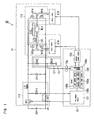
- FIG.1 shows a first basic concept, i.e., a discharge lamp ballast 10 for an HID lamp (e.g., extra-high-pressure mercury discharge lamp of 120-300 W) DL1, however not showing each feature of the present invention.
- the ballast 10 comprises a resistor R11 for detecting an input current, a state detection circuit 12, a control circuit 13 and an igniter (not shown), and further comprises a power converter 11 connected between a DC power source DC1 with a positive terminal and a negative terminal and an HID lamp DL1 with a first terminal and a second terminal.
- the igniter In order to start the lamp DL1, the igniter generates and applies high voltage to the lamp DL1.
- the power converter 11 comprises a DC-DC converter 111, an LC series circuit 112, an inverter 113 with output terminals T11 and T12, and drive circuits 114 and 115, and further comprises a capacitor (smooth condenser) C11 that provides DC power from the DC-DC converter 111 for the lamp DL1.
- a capacitor smooth condenser
- the DC-DC converter 111 can be constructed of, for example, a voltage step down converter having a diode D11, a switching element Q11 and an inductor L11.
- the diode D11 has a cathode and an anode, and the anode is connected to the negative terminal of the DC power source DC1 via the resistor R11, and also connected to the negative voltage side of the capacitor C11.
- the switching element Q11 is connected between the cathode of the diode D11 and the positive terminal of the DC power source DC1.
- This element Q11 is a power MOSFET with a diode (body diode), and its drain and source are connected to the positive terminal of the source DC1 and the cathode of the diode D11, respectively.
- a cathode and an anode of the body diode are also connected to the drain and the source of the power MOSFET, respectively.
- the inductor L11 is connected between the cathode of the diode D11 and the positive voltage side of the capacitor C11.
- This DC-DC converter 111 flows a charging current from the DC power source DC1 to the capacitor C11 through the inductor L11 during turn-on of the switching element Q11, and releases energy in the inductor L11 to the capacitor C11 via the diode D11 during turn-off of the switching element Q11.
- the LC series circuit 112 is constructed of a capacitor C12 connected in parallel with the lamp DL1 and an inductor L12 connected in series with the combination of the lamp DL1 and the capacitor C12, and is connected between the output terminals T11 and T12 of the inverter 113.
- the inverter 113 is constructed of switching elements Q12-Q15, and converts DC voltage from the capacitor C11 into square wave voltage to be applied across the LC series circuit 112 and thereby provides AC power for the lamp DL1.
- Each of the elements Q12-Q15 is a power MOSFET with a diode (body diode).
- the element Q12 is connected to the positive voltage side, and its drain and source are connected to the positive voltage side (positive terminal) of the capacitor C11 and the output terminal T11, respectively.
- the element Q13 is connected to the negative voltage side, and its drain and source are connected to the output terminal T11 and the negative voltage side (negative terminal) of the capacitor C11, respectively.
- the element Q14 is connected to the positive voltage side, and its drain and source are connected to the positive terminal of the capacitor C11 and the output terminal T12, respectively.
- the element Q15 is connected to the negative voltage side, and its drain and source are connected to the output terminal T12 and the negative terminal of the capacitor C11, respectively.
- the drive circuits 114 and 115 are constructed of, for example, IR2111 made by IR company each, and alternately turns the switching elements Q12 and Q15 and the switching elements Q13 and Q14 on/off in response to control signals from the control circuit 13.
- the state detection circuit 12 includes a voltage division circuit 121 having resistors R12 and R13 that are connected in series, and detects a state of the lamp DL11.
- the circuit 121 is connected in parallel with the capacitor C11 and the resistor R11. Voltage across the resistor R13 is proportional to output voltage of the DC-DC converter 111 (voltage across the capacitor C11), and represents lamp voltage across the lamp DL1. Accordingly, the circuit 12 detects the output voltage of the converter 111 and the lamp voltage.
- the control circuit 13 includes an A/D converter 13a, a PWM (pulse width modulation) control circuit 131, an inverter control circuit 132 and a micon (microcomputer) 130.
- the circuit 13 respectively monitors an input current and the output voltage of the DC-DC converter 111 (or lamp voltage) by monitoring voltage across the resistor R11 and voltage across the resistor R13, and controls an on/off state of each switching element of the power converter 11 based on the input current and the output voltage (lamp voltage).
- the A/D converter 13a converts detection result of the state detection circuit 12 (output voltage of the DC-DC converter 111 or lamp voltage) into digital.
- the voltage across the resistor R13 is directly applied to the converter 13a because it is proportional to voltage smoothed through the capacitor C11 and constant within a sampling period of the converter 13a.
- the PWM control circuit 131 generates a pulse shaped control signal from triangular wave or saw tooth wave voltage having a prescribed frequency in response to a target current or correction quantity on output power of the DC-DC converter 111 from the micon 130, and provides the control signal for the switching element Q11.
- the circuit 131 generates the control signal for equalizing the input current from the resistor R11 with the target current. Since the input current from the resistor R11 represents the output current of the converter 111, the output current is made equal to the target current.
- the circuit 131 finds correction quantity on the output voltage by dividing the correction quantity on the output power by the input current from the resistor R11 (output current of converter 111), and generates a control signal that becomes turn-on (High) when the triangular wave or saw tooth wave voltage equals or exceeds threshold voltage varied in response to the correction quantity on the output voltage.
- the inverter control circuit 132 generates two phases of control signals according to drive instruction from the micon 130, and provides the signals for the drive circuits 114 and 115, respectively.
- the micon 130 is constructed of, for example, a M37540 made by Mitsubishi company, and has a function for providing the above drive instruction for the inverter control circuit 132 after the start of the lamp DL1.
- the micon 130 has various functions such as a control changeover function 130a, a lamp current control function 130b, a constant power control function 130c, a high power control function 130d and so on.
- the micon 130 also stores data such as various tables, various target values and so on.
- the control changeover function 130a is operable to change control for the lamp DL1 to lamp current control of the lamp current control function 130b at the start of the lamp DL1, and then change the lamp control to constant lamp power control of the constant power control function 130c at stabilization of the lamp DL1.
- the stabilization of the lamp DL1 is judged based on the detection result from the A/D converter 13a (the output voltage). Namely, lamp voltage immediately after the start of the lamp DL1 is low voltage, and therefore a start time period is set for a period of time that voltage across the resistor R13 is lower than reference voltage.
- the reference voltage is previously set based on voltage across the lamp DL1 in its stable operation. Accordingly, when the voltage across the resistor R13 reaches or exceeds the reference voltage, the lamp DL1 is judged to reach a stable state.
- the control changeover function 130a is also operable to change lamp power control to constant lamp power control or high power control based on the detection result from the A/D converter 13a (lamp voltage) after stabilization of the lamp DL1. A detailed explanation of this is given later.
- the lamp current control function 130b is operable to supply a target current for lamp current control to the PWM control circuit 131 according to changeover control of the control changeover function 130a.
- a target value of the target current is set to a value for flowing a comparatively large lamp current (current larger than the rated lamp current) in a prescribed time period immediately after the start. Since this lamp current control raises mercury vapor pressure and the light output of the lamp DL1 in a short time, such control is generally utilized for projectors or headlights of automobiles.
- the constant power control function 130c is operable to supply correction quantity on output (lamp) power for the constant lamp power control to the PWM control circuit 131 according to the changeover control of the control changeover function 130a.
- the correction quantity is to adjust an effective value of lamp power provided for the lamp DL1 to a prescribed power value (rated power value or dimming power value).
- the correction quantity is calculated based on the detection result from the A/D converter 13a (the output voltage) and a table for the constant lamp power control. In the table for the constant lamp power control, each detection result from the converter 13a (output voltage value) is previously related to an output (lamp) power control value.
- the function 130c converts the detection result into an output power control value by reading out the output power control value corresponding to the detection result from the table for the constant lamp power control, and finds difference between the output power control value and the output (lamp) power target value, as the correction quantity on output power.
- This constant lamp power control is generally changed in order to stably keep lamp power of the lamp DL1 during steady operation after the lamp current control of the lamp current control function 130b.
- the high power control function 130d is operable to supply correction quantity on output power for the high power control to the PWM control circuit 131 according to the changeover control of the control changeover function 130a.
- the correction quantity is to increase at least one of an effective value and a peak value of the lamp power provided for the lamp DL1 more than that adjusted with the constant power control function 130c.
- the correction quantity is calculated based on the detection result from the A/D converter 13a (the output voltage) and a table for the high power control.
- the high power control function 130d also utilizes an output power target value larger than that of the constant power control function 130c. For example, as shown in FIG. 2 , any output power target value is selected and utilized from output power target values in case of the rated power or each dimming power.
- the constant power control function 130c utilizes a first rated target as an output power target value
- the high power control function 130d utilizes a second rated target and a third rated target of output power target values.
- output power is set to output power P HC11 larger than the rated power P RL1 .
- output power is set to output power P HC12 larger than the output power P HC11 .
- the second rated target or the third rated target is set based on a prescribed condition such as, for example, ambient temperature or the like. In case that ambient temperature is utilized as the prescribed condition, the second rated target is selected when ambient temperature is lower than first reference temperature, and the third rated target is selected when ambient temperature is lower than second reference temperature that is lower than the first reference temperature.
- the constant power control function 130c utilizes a first dimming target as an output power target value
- the high power control function 130d utilizes a second dimming target and a third dimming target of output power target values.
- the second dimming target larger than the first dimming target
- output power is set to output power P HC21 larger than dimming power P D1
- the third dimming target larger than the second dimming target
- output power is set to output power P HC22 larger than the output power P HC21 .
- the second dimming target or the third dimming target is set based on a prescribed condition such as, for example, ambient temperature or the like. In case that ambient temperature is utilized as this prescribed condition, the second dimming target is selected when ambient temperature is lower than first reference temperature, and the third dimming target is selected when ambient temperature is lower than second reference temperature that is lower than this first reference temperature.
- the above control changeover function 130a is further explained.
- the function 130a changes lamp power control to the high power control when the lamp voltage (voltage across R13) reaches or exceeds threshold voltage V t1 that is higher than the rated lamp voltage V RL1 , and changes lamp power control to the constant lamp power control when the lamp voltage is less than the threshold voltage V t1 .
- the threshold voltage V t1 for the rated operation may be the same as or different from that for the dimming operation.
- VR CC1 represents a voltage range in the start time period
- VR PC1 represents a voltage range utilized after the start time period of the lamp DL1 and this range is set so as to include the voltage V RL1 at intermediate portion thereof.
- the lamp current control is changed to the constant lamp power control.
- the first basic concept i.e., the ballast 10 is able to prevent decrease of temperature of the electrodes or within the bulb.
- the control changeover function 130a is operable to change lamp power control to the high power control over a prescribed time period TM HC1 , and change lamp power control to the constant lamp power control after the prescribed time period TM HC1 is passed.
- the prescribed time period is included in a period of time while the detection result of the state detection circuit 12 is equal to or higher than the threshold voltage V t1 .
- timing for returning the high power control to the constant lamp power control is controlled by using a timer function of the micon, i.e., time.
- t1 shows a point in time that the detection result of the state detection circuit 12 reaches the threshold voltage V t1 .
- the control changeover function 130a is operable: to change control for the lamp DL1 to the lamp current control after the start of the lamp DL1; to change lamp power control to the high power control for a prescribed time period TM HC2 immediately after reaching a stable state of the lamp DL1 (near after reaching the stable state); and to change lamp power control to the constant lamp power control after the prescribed time period TM HC2 .
- this changeover control since the lamp current is increased for a period of time such as needed for stabilization of electrode temperature of the lamp DL1 from the start of arc discharge, temperature of the electrodes or within the bulb can be raised rapidly and the temperature can be stabilized easily.
- the control changeover function 130a is operable to change control for the lamp DL1 to the lamp current control after the start of the lamp DL1, and change lamp power control to the high power control or the constant lamp power control alternately and periodically after reaching a stable state of the lamp DL1.
- TM H-C shows a period of changeover of the high power control and the constant lamp power control.
- FIG. 7 shows a second basic concept, i.e., a discharge lamp ballast 20 for an HID lamp (e.g., extra-high-pressure mercury discharge lamp of 120-300 W) DL2, however not showing each feature of the present invention.
- the ballast 20 is characterized by a state detection circuit 22 and a control circuit 23, and different from the first basic concept in that the state detection circuit 12 is constructed of the voltage division circuit 121 and the control circuit 13 is constructed of the A/D converter 13a, the micon 130, the PWM control circuit 131 and the inverter control circuit 132.
- the state detection circuit 22 comprises a voltage division circuit 221 similar to the voltage division circuit 121, and also comprises a resistor R24 with small resistance, a current detection circuit 222 and a light output detection circuit 223.
- the resistor R24 is connected between a negative voltage side of a capacitor C21 (negative terminal) and sources of switching elements Q23 and Q25, and detects voltage corresponding to a lamp current through the lamp DL2. Voltage across the resistor R24 is low voltage due to the small resistance and fluctuates with switching of a inverter 213. On account of this, the current detection circuit 222 is provided.
- This circuit 222 includes a filter and an amplification circuit, and appropriately amplifies the voltage across the resistor R24.
- the light output detection circuit 223 includes a light receiving element such as, for example, a photodiode or the like, and is located in proximity to the lamp DL2 to detect a light output of the lamp DL2.
- the control circuit 23 comprises A/D converters 23b and 23c, and a micon 230 in addition to an A/D converter 23a, a PWM control circuit 231 and an inverter control circuit 232.
- the converter 23b converts an analog output corresponding to a lamp current from the current detection circuit 222 into digital.
- the converter 23c converts an analog output representing a light output of the lamp DL2 from the light output detection circuit 223 into digital.
- the micon 230 is characterized by a control changeover function 230a including a timer function and a flicker detection function in comparison with the micon 130 of the first basic concept.
- the timer function of the function 230a is utilized for a time limit of the high power control, and operable to time a prescribed time period.
- the flicker detection function of the function 230a is operable to use each digital value from the A/D converters 23a-23c every time period TM between neighboring polarity inverting timings of output voltage (square wave voltage) of the inverter 213 Accordingly, it is possible to eliminate digital values under influence of overshoot at polarity inverting from each digital value of the converters 23a-23c, so that it is possible to use digital values without influence of the overshoot.
- the start timing of the time period TM is set for, for example, a point in time after a prescribed time from the polarity inverting of rising.
- the flicker detection function may hold a value of detection factor every period of output voltage of the inverter 213, calculate a mean value of the values of the detection factors over the periods, and use the mean value.
- the flicker detection function of the function 230a is also operable to detect flicker generation on the lamp DL2 based on each detection result of the state detection circuit 22.
- the flicker generation is detected based on at least one of digital values corresponding to the lamp voltage from the A/D converter 23a, digital values corresponding to the lamp current from the A/D converter 23b and digital values corresponding to the light output of the lamp DL1 from the A/D converter 23c.
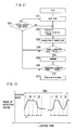
- the flicker detection function reads digital values (values of detection factors) from each of the A/D converters 23a-23c (S11), and finds change value in its digital output per unit time ⁇ t (S12). In case that this change vale is equal to or larger than a prescribed value (reference value), the function detects flicker generation. For example, when digital values corresponding to the lamp voltage change such as V DLt1 , V DLmin , ..., V DLmax , V DLt2 , etc, the change value is calculated from an absolute value of difference between the maximum value V DLmax and the minimum value V DLmin .
- the unit time ⁇ t may be the time period TM of FIG. 8 .
- the change value is not limited to that of FIG. 10(b) , and may be substituted by a value such as an absolute value of difference between two digital values that are continuously picked up at sampling period of the A/D converter, or the like.
- the control changeover function 230a changes lamp power control to the high power control for a prescribed time period through the timer function, and changes lamp power control to the constant lamp power control after the prescribed time period is passed.
- ballast 20 The operation of the ballast 20 is now explained.
- control for the lamp DL2 is changed to the lamp current control.
- the lamp current control is changed to the constant lamp power control.
- the constant lamp power control is changed to high power control for the prescribed time period.
- the ballast 20 changes the constant lamp power control to the high power control based on detection of flick generation, and therefore it is possible to prevent decrease of the temperature of the electrodes or within the bulb. Also, since the decrease of the temperature of the electrodes or within the bulb causes visible flicker, the flicker generation can be prevented. Even if flicker immediately stops after the constant lamp power control is changed to the high power control, the high power control is continued for the prescribed time period, so that the temperature of the electrodes or within the bulb can be raised sufficiently. Inversely, if flicker does not stop during the prescribed time period, the high power control is changed to the constant lamp power control, and therefore it is possible to prevent useless power consumption occurred by increasing power over needlessly long hours.
- ballast 20 is utilized for lighting, the lighting that gives little flicker and does not bring discomfort is possible.
- the ballast 20 is utilized for a projector such as a liquid crystal projector or the like, even if its light source is a light source that is approximate to a point source, it is possible to obtain a stable light output with little flicker.
- control changeover function 230a changes lamp power control to the high power control in case that the flicker detection function detects flicker generation, and changes lamp power control to the constant lamp power control in case that flicker generation is not detected.
- This changeover control can be added to the second basic concept, and any control can be selected.
- the flicker detection function of the function 230a detects flicker generation when a change value in at least two detection factors per unit time is equal to or greater than a prescribed value.
- the flicker detection function of the function 230a finds the number of cases in which the above change value becomes equal to or greater than the above prescribed value every judgment time period longer than the unit time, and detects flicker generation when the number of cases is equal to or greater than a specified number of times (threshold value).
- a specified number of times threshold value.
- visible flicker occurs in case that the light output varies at a frequency within 3-15 Hz, and therefore it is preferable that the judgment time period TM1 is set for 1 second and the threshold value is set within the range of 3-15 times.
- an enumerated value is first reset at step S21.
- a value of detection factor in unit time ⁇ t is then read (S22), and a change value is calculated (S23).
- the change value is then compared with the prescribed value (S24). When the change value is equal to or larger than the prescribed value (YES at S24), increment, for example, 1 (see FIG. 12 ) is added to the enumerated value (S25), and step S26 is proceeded to.
- step S28 is proceeded to.
- step S26 when the enumerated value is equal to or larger than the threshold value (YES at step 26), flicker generation is detected (S27).
- step S28 is proceeded to.
- step S28 the step is returned to step S22 when time elapsed is within the judgment time period TM1 (YES at S28), where the time elapsed is time elapsed from a point in time that the enumerated value is reset (S21), and is given by ⁇ t ⁇ "the number of times that step S28 is proceeded to".
- the step is returned to step S21.
- the high power control function 230d is operable to control the on/off period of the switching element of the DC-DC converter 211 so as to increase the lamp current I DL provided by component of at least a half-period of the square wave voltage while the number of half-period pulses of the square wave voltage reaches a specified number of times.
- a time period Tn or Tw for increasing the lamp current I DL is set for time that is different from the other time period Tu.
- the time period Tn is set shorter than the other time period Tu
- the time period Tw is set longer than the other time period Tu. Since the increase rate of the lamp current I DL and the time of the half period depend on the ballast, it is possible to supply a desired lamp current I DL to the lamp DL2 by increasing or decreasing the time period Tn or Tw for increasing the lamp current I DL . For example, in case of an HID lamp that is subjected to a harmful influence on the electrodes when the time period Tn equals the other time period Tu, the influence on the electrodes can be reduced by making the time period Tn shorter than the time period Tu.
- time period Tw is made equal to the time period Tu, there are cases in which required energy can not be supplied to the lamp because the lamp current I DL of the lamp has the upper limit value, but it is possible to cope with that by making the time period Tw longer than the time period Tu.
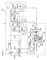
- FIG. 14 shows a third basic concept, i.e., a discharge lamp ballast 30 for an HID lamp (e.g., extra-high-pressure mercury discharge lamp of 120-300 W) DL3, however not showing each feature of the present invention.
- the ballast 30 is characterized by a control circuit 33, and different from the first basic concept in that the control circuit 13 is constructed of the A/D converter 13a, the micon 130, the PWM control circuit 131 and the inverter control circuit 132.
- control circuit 33 comprises a micon 330 and an integration circuit 333 in addition to an A/D converter 33a, a PWM control circuit 331 and an inverter control circuit 332.
- the micon 330 is characterized by a high power control function 330d with a non-correction control function 330H and a correction control function 330E, and a control changeover function 330a in comparison with the micon 130 of the first basic concept.
- the non-correction control function 330H is operable to control the on/off state of the switching element Q31 so that a part of lamp power provided for the lamp DL3 is increased more than that adjusted by the constant lamp power control of the constant power control function 330c.
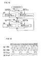
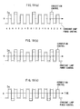
- the function 330H provides the integration circuit 333 with a pulse signal I DLup for power increase in order to increase the peak value (wave height value) of part of the lamp current I DL , and thereby increases the effective value of the lamp current I DL .
- the signal I DLup is provided m-times to the circuit 333 while the number of half-period pulses of output voltage of the inverter 313 reaches a specified number of times n, where m and n are integers.
- n and n are set to 1 and 5, respectively.
- the control in the period of time that the signal I DLup is not provided is the same as the constant lamp power control, and therefore the effective value of the lamp current I DL increases in response to the period of time that the signal I DLup is provided.
- the function 330H may provide two times (first and third half-periods) the signal I DLup for the circuit 333 while the number of half-period pulses reaches 5.
- n the effective value of the positive and negative lamp current I DL can be increased, and it is possible to make electrodes of the lamp DL3 substantially equal in degradation.
- FIG. 17(b) the control in the period of time that the signal I DLup is not provided is the same as the constant lamp power control, and therefore the effective value of the lamp current I DL increases in response to the period of time that the signal I DLup is provided.
- the function 330H may provide two times (first and third half-periods) the signal I DLup for the circuit 333 while the number of half-period pulses
- the function 330H may provide once the signal I DLup for the circuit 333 while the number of half-period pulses reaches 6.
- n the number of half-period pulses
- the correction control function 330E is operable to control the on/off state of the switching element Q31 so that a part of lamp power provided for the lamp DL3 is increased more than that adjusted by the constant lamp power control of the function 330c while equalizing the effective value of the lamp power provided for the lamp DL3 with that adjusted by the constant lamp power control.
- the function 330E provides the integration circuit 333 with a pulse signal I DLup for power increase while providing the circuit 333 with a Vref adjustment signal for adjusting the level of DC voltage Vref applied to the PWM control circuit 331 from the circuit 333.
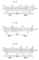
- the signal I DLup is provided for the circuit 333 and thereby the effective value of the lamp current I DL is increased as well, but by providing the Vref adjustment signal for the circuit 333, wave height values of the lamp current I DL in the whole period of time are decreased in response to increment of the effective value of the lamp current I DL by the signal I DLup .
- FIGs. 18(a) and 18(b) correspond to FIGs. 17(a) and 17(b) , respectively. In another example, as shown in FIG.
- the function 330E may provide twice (first and fifth periods) the signal I DLup for the circuit 333 while the number of half-period pulses reaches 7.
- the parameter n for the signal I DLup may be set to an even number.
- m and n are set to 6 and 1, respectively.
- m and n are set to 6 and 2, respectively.
- m and n are 6 and 1, respectively and the polarity of increased lamp current is inverse polarity as compared with FIG. 19(a) .
- the control changeover function 330a is operable to change to control of the non-correction control function 330H or the correction control function 330E based on various changeover conditions (S31 in FIG. 15 ).
- the function 330a changes lamp power control to the control of the function 330H based on a non-correction changeover condition, namely, in case that the lamp voltage reaches or exceeds a threshold voltage (cf. Vt1 in FIG. 3 ).
- the function 330a also changes lamp power control to the control of the function 330E based on a correction changeover condition, namely, in case of a shift to dimming operation.
- control changeover function may change lamp power control to the control of the non-correction control function when the light output detection circuit detects flicker generation. Also, the function may change lamp power control to the control of the correction control function when a change value in digital output from a voltage division circuit or a current detection circuit is equal to or larger than a prescribed value, or when shifting a dimming operation.
- the integration circuit 333 is constructed of resistors R34 and R35, a diode D32 and a capacitor C33, and located between the micon 330 and the PWM control circuit 331.
- a pulse signal Vref adjustment signal
- the pulse signal is converted into DC voltage Vref through the resistor R34 and the capacitor C33.
- the signal I DLup also flows from the micon 330 to the resistor R35, the DC voltage Vref provided for the circuit 331 is increased in response to the signal I DLup .
- the micon 330 when the micon 330 provides the inverter control circuit 332 with two phases of signals FB1 and FB2 according to the timing of FIG. 16 , the micon 330 (function 330H or 330E) counts the number of polarity inversions through the signals FB1 and FB2, where FB1 and FB2 are similar to control signals given from the circuit 332 to drive circuits 314 and 315. According to the timing of FIG. 16 , the micon 330 then provides the resistor R35 with the signal I DLup that synchronizes with the signals FB1 and FB2. Accordingly, voltage (DC voltage Vref) across the capacitor C 33 rises. The lamp current detected through the resistor R31 is controlled to be more increased as the DC voltage Vref is higher. Increment of the lamp current according to the signal I DLup is adjusted through resistance of the resistor R35.
- Efficiency of increase of the lamp current I DL is low when time of half period for increasing the current I DL is short, and load on the electrodes is large when the time of half period is long, so that it is preferable that the time is set for about 0.5-50 ms.
- the lamp current I DL in a half period when the current I DL is not increased is utilized as a reference value, and an increase rate of the current I DL is set to be increased about 5-60% with respect to the reference value.
- n and the increase rate were respectively 5 and 30 %, and the lamp DL13 was operated for one hour while increasing the peak value of the lamp current I DL in a half period more than that in the other period of time while the number of half-period pulses of output voltage reached 5.
- the peak value of the lamp current I DL was kept to be constant, arc jumping occurred over a comparatively long time.
- the arc jumping means a phenomenon that end position of the arc is not stable and moves here and there, resulting change in the light output. On the contrary, in case of the non-correction control, arc jumping did not occur.
- the ballast 30 is able to prevent flicker generation by changing to the control of the non-correction control function 300H, and also to prevent flicker generation and variation of the light output by changing to the control of the correction control function 330E.
- the micon 330 comprises only the correction control function 330E in the high power control function 330d.
- the control changeover function 330a changes lamp control to the lamp current control till the lamp voltage reaches voltage of the rated lower limit (see table 1 described later) of the rated lamp voltage after the start of the lamp DL3, and also changes lamp power control to the correction control or the constant lamp power control in case of rated operation and dimming operation.
- the function 330a changes to the correction control of the function 330E when the lamp voltage is voltage within the rated range (see table 1 described later), and also changes to the constant lamp power control of the constant power control function 330c when the lamp voltage is voltage lower than the voltage of the rated lower limit.
- This control is suitable for projectors. For example, when temperature within a projector rises and lamp voltage drops to voltage lower than the voltage of the rated lower limit, lamp power control is changed from the correction control of the high power control to the constant lamp power control and therefore the temperature within the projector can be lowered.
- FIG. 20 shows an embodiment of the present invention, i.e., a discharge lamp ballast 40 for an HID lamp (e.g., extra-high-pressure mercury discharge lamp of 120-300 W) DL4.
- the ballast 40 is characterized by a control changeover function 430a and a high power control function 430d of a micon 430, and is not provided with a constant power control function in the maicon 430 as compared with the second basic concept.
- the control changeover function 430a is operable to change to first high power control (cf. a period of time TM HC11 of FIG. 21 ) of the high power control function 430d at stabilization of the lamp DL 4, and change lamp power control to the first high power control or second high power control (cf. a period of time TM HC12 of FIG. 21 ) of the function 430d based on detection result of the state detection circuit 42.
- the high power control function 430d is operable to control the on/off state of the switching element Q41 so that at least one of an effective value and a peak value of the lamp power provided for the lamp DL4 is increased more than that adjusted by constant lamp power control based on the first high power control.
- the function 430d is also operable to change frequent degree of increase of the lamp current through the lamp DL4 so that lamp power under the second high power control becomes larger than that under the first high power control based on the second high power control.
- control changeover function 430a changes the first high power control to the second high power control according to shift conditions from the first high power control to the second high power control, namely, in case that lamp voltage is within a specified range (from threshold voltage to the upper limit voltage with respect to circuit operation) in dimming operation, in case that a supply of power to the HID lamp is reduced, in case that prescribed time passes after the lamp turn-on, in case that accumulated lighting time of the lamp reaches prescribed time, or in case that flicker or arc jumping is detected.
- the function 430a changes the second high power control to the first high power control according to shift (return) conditions from the second high power control to the first high power control, namely, in case that lamp voltage is out of the specified range and lower than the lower limit during dimming operation, in case that a supply of power to the lamp is increased, in case that prescribed time passes after shift from the first high power control to the second high power control, or in case that flicker or arc jumping is not detected.
- an alternative condition that prescribed time passes after shift to the second high power control owing to flicker or arc jumping may be utilized.
- the accumulated lighting time is measured with a timer that accumulates lighting time (from power on to power off) of the HID lamp.
- a timer that accumulates lighting time (from power on to power off) of the HID lamp.
- generation of arc jumping can be detected when the difference continuously exceeds a threshold value for prescribed time.
- the flicker detection function is utilized for detection of arc jumping.
- the accumulated lighting time is increase only, and is not included in the return conditions.
- the table 1 is obtained by summarizing relation between the first high power control and the second high power as well as lamp voltage and prescribed power (rated operation or dimming operation) of the lamp.
- the "Rated range” means a range including rated lamp voltage in consideration of dispersion in characteristics of HID lamps.
- the rated lower limit and the rated upper limit correspond to the lower limit and the upper limit of the rated range, respectively.
- the above frequent degree is next explained.
- change methods of the frequent degree as shown in FIG. 21 , besides a method that the above parameter (specified number of times) n is changed, there is a method that the number of times (m) of increase of the lamp current per unit period of time is changed.
- the high power control function 430d increases the lamp current only for one half period while the number of half-period pulses of square wave voltage reaches 5.
- the function 430d increases the lamp current only for one half period while the number of half-period pulses of square wave voltage reaches 3.
- Such changeovers may be at least three sorts of changeovers.
- the unit period of time may be set for a period of time that the number of half-period pulses reaches 5, and the lamp current of each half period of two inversions in the unit period of time may be increased more than that of the other period of time in the unit period of time.
- the dimming operation it is necessary to adjust amplitude of the square wave voltage so that the effective value of the lamp current lowers more than that of the rated operation.
- the ballast 40 changes lamp power control to the first high power control or the second high power control from stabilization of the lamp DL4 and therefore flicker generation and variation of the light output can be prevented.
- the high power control function 430d is operable to change peak (wave height value) of the lamp current through the lamp DL4 so that lamp power under the second high power control is larger than that under the first high power control.
- the peak value of lamp power under the second high power control is set larger than that under the first high power control, and the effective value of lamp power under the second high power control is set to be equal to that under the first high power control.
- Such changeovers may be at least three sorts of changeovers.
- third high power control is prepared, its peak value is made larger than that of the second high power control, and the effective value of lamp power under the high power control is made equal to that under the first or the second high power control.
- any of the first high power control to the third high power control can be selected based on detection result of the state detection circuit 42.
- the high power control function 430d in case of changeover from the first high power control to the second high power control, is operable to change frequent degree of increase of the lamp current and peak of the lamp current so that lamp power under the second high power control is larger than that under the first high power control.
- the target output range can be also spread and, for example, a dimming range can be spread.
- FIG. 24 shows a projector equipped with a discharge lamp ballast.
- this projector includes any discharge lamp ballast of the above embodiments, the HID lamp as a light source and a color filter 14 whose transmission color by light from the light source is timewise changed with a prescribed period, and operates with, for example, DLP (registered trademark) system that utilizes DMD (digital micro mirror device).
- DLP registered trademark
- the ballast, the lamp and the filter 14 are enclosed in a housing 16 together with a projection lens 15, the DMD, fan(s) and so on.
- the color filter 14 is a disk shape and located in front of the light source, and light that passes through the filter 14 is reflected at the DMD.
- the filter 14 is divided into regions of red (R), green (G), blue (B) and colorless (W), and rotates at a constant period in direction of the arrow X of FIG. 25 . Accordingly, as shown in (a) of Fig. 26 , transmission color of the filter 14 changes such as red (R), green (G), blue (B) and colorless (W) as time elapses.
- Timing for changing polarity of voltage applied across the light source is synchronized with borders of each color region in the filter 14. Accordingly, light that passes through each color region in the filter 14 does not become light whose light output is dropped at changeover of the polarity, so that it is possible to efficiently utilize light emitted from the light source.
- the red region is larger than any of the other regions in area, and the period of time that light from the light source passes through the red region is longer than a period of time that light from the light source passes through any of the other regions. Therefore, in the period of time that the light passes through the red region, the polarity is changed.
- the lamp current I DL is increased more than that in any of the other period of times, but in a period of time that the light passes through one of the other regions, the lamp current may be increased more than that in another of the other period of times. In period of times corresponding to at least two regions, the lamp current may be also increased more than that in another of the other period of times.
- the effective value of the lamp current I DL under the high power control (solid line) is set to a value larger than that under the constant lamp power control (broken line).
- the effective value of the lamp current I DL under the high power control (solid line) is set to a value equal to that under the constant lamp power control (broken line).
- a color filter without colorless region (W) can be replaced with the filter 14. But not limited to the projector, each ballast of the above embodiments can be used for various projectors.
- the embodiments include power MOSFETs, but in addition to switching elements such as IGBTs or the like, bipolar transistors and diodes may be used instead of the power MOSFETs.
- the DC power source may be a DC power source that rectifies AC power.
- the embodiments include the voltage step down converters since voltage of each DC power source DC1 is higher than lighting voltage of each HID lamp, but a DC-DC converter with other construction (e.g., voltage step up/down converter including switching elements) may be used instead of the voltage step down converter in response to the sort of the lamp.
- the embodiments include inverters, but in case that an HID lamp is a DC lamp, it is possible to omit the inverter.
Landscapes
- Engineering & Computer Science (AREA)
- Multimedia (AREA)
- Signal Processing (AREA)
- Circuit Arrangements For Discharge Lamps (AREA)
Abstract
Description
- The invention relates to discharge lamp ballasts utilized for operating high intensity discharge lamps (HID lamps), and projectors equipped with the discharge lamp ballasts.
- In conventional discharge lamp ballasts, HID lamps are operated by, for example, square wave voltage. In case of an extra high pressure mercury lamp utilized as a light source for a projector, square wave voltage with a comparatively low frequency (approx. 100s Hz) is applied across the lamp in order to prevent occurrence of acoustic resonance phenomenon (see, e.g., Japanese Patent Application Publication number
2002-352982 - In these sorts of applications, arc length of the lamp is required to be as short as possible in order to approximate it to a point source. However, if the arc length is shortened, an arc generation point on an electrode gets unstable depending on temperature or surface condition of the electrode, so that the phenomenon that the arc origin point jumps to other points is easy to occur. When this sort of phenomenon occurs, visible flicker is perceived in light output of the lamp, and in case that the lamp is utilized as a light source for a projector, problems are raised, such as difficulty seeing screen image due to brightness fluctuation or luminance reduction on plane of projection (screen), or the like.
- By the way, when lamp voltage across an HID lamp is high, its lamp current decreases and temperature of electrodes and within a bulb of the lamp decreases, and therefore active chemical characteristics within the bulb are suppressed. When such phenomenon occurs in a metal halide lamp, its halogen cycle does not get active. Usually, a protrusion is formed on the surface of the electrode, and the protrusion serves as an arc origin so that the arc origin is stabilized, but the protrusion is hard to be formed on the surface of the electrode in condition that the active chemical characteristics within the bulb are suppressed as described above. On account of this, the arc origin is not fixed, and the phenomenon that the arc origin moves is easy to occur. Also, if a protrusion is not formed on the surface of the electrode and the arc origin does not stabilize, the whole electrode suffers damage by the arc, resulting in early electrode degradation.
- Incidentally, a technology for reducing flicker of a discharge lamp is suggested in, for example, Japanese Patent National Publication number
2002-532866 - A technology suggested in Japanese Patent Application Publication number
2002-134287 - According to the technologies described in the Patent Application Publication number
2002-352982 2002-532866 , electrode wear is controlled. The latter especially directs its attention to reduction of flicker, but there is a need to superpose a pulse-shaped current in order to modify the shape of the lamp current through the lamp, so that comparatively complicate control is required. - A technology described in the Patent Publication number
2002-134287 changes the instantaneous value of power supplied to the lamp and also changes each wave form of voltage applied across the lamp or the lamp current into wave form except square wave. Therefore, comparatively complicate control is required. - It is therefore an object of the present invention to maintain temperature of electrodes of an HID lamp and to stabilize of light output in addition to keeping temperature within the lamp in a proper state through simple control.
- Another object of the present invention is to stabilize an arc origin point by promoting formation of a protrusion on an electrode, and thereby prevent flicker generation and electrode degradation to extend life of an HID lamp.
- A discharge lamp ballast of the present invention comprises a power converter and a control circuit. The converter includes at least one switching element and is connected between a power source and an HID lamp. After the start of the lamp, the control circuit controls an on/off state of the switching element so as to provide prescribed lamp power for the lamp based on lamp power control. The control circuit controls the on/off state of the switching element so that at least one of an effective value and a peak value of the lamp power provided for the lamp is increased more than that adjusted by constant lamp power control based on high power control after the start of the lamp. The constant lamp power control is control for adjusting the effective value of the lamp power provided for the lamp to a prescribed power value. Thus, by controlling the on/off state of the switching element based on the high power control, it is possible to keep temperature of electrodes or within a bulb of the lamp in a proper state. As a result, since formation of a protrusion on the electrode can be promoted and an arc origin point can be stabilized, flicker generation and electrode degradation are prevented and the life of the lamp can be extended. In an aspect of the invention, the power converter comprises: a converter that includes the switching element and converts voltage from the power source into DC voltage; and an inverter that includes switching elements and inverts the DC voltage from the converter into square wave voltage. In this configuration, the control circuit controls the on/off period of the switching element of the converter so as to increase a lamp current provided by component of at least a half-period of the square wave voltage while the number of half-period pulses of the square wave voltage reaches a specified number of times, in case of the high power control. As a result, temperature of the electrodes of the lamp can be maintained, and stabilization of light output is possible.
- The control circuit may control the on/off period of the switching elements of the inverter so that time of half-period in which the lamp current is increased differs from time of half-period in which the lamp current is not increased. Since time for increasing the lamp current is also adjusted in addition to increase of the lamp current, compatibility between fitness for specification of the lamp and retention of electrode temperature is possible by adjusting the time even in case that it is difficult to achieve the compatibility only by the lamp current.
- It is desirable that the ballast comprises a state detection means that detects a state of the lamp and the control circuit changes frequent degree of increase of the lamp current based on the detection result of the state detection means when the lamp current provided by the component of at least a half-period of the square wave voltage is increased. According to this control, since frequent degree of increase of the lamp current is also adjusted in addition to increase of the lamp current, compatibility between fitness for specification of the lamp and retention of electrode temperature is possible by adjusting the frequent degree even in case that it is difficult to achieve the compatibility only by the lamp current.
- The ballast may comprise a state detection means that detects a state of the lamp, and the control circuit may change peak of the lamp current based on the detection result of the state detection means when the lamp current provided by the component of at least a half-period of the square wave voltage is increased. According to this control, since a peak value of the lamp current is also adjusted in addition to increase of the lamp current, compatibility between fitness for specification of the lamp and retention of electrode temperature is possible by adjusting the peak value even in case that it is difficult to achieve the compatibility only by the lamp current.
- Preferably, the ballast comprises a state detection means that detects a state of the lamp, and the control circuit changes frequent degree of increase of the lamp current and peak of the lamp current based on the detection result of the state detection means when the lamp current provided by the component of at least a half-period of the square wave voltage is increased. According to this control, the adjusting range becomes wider.
- A projector of the present invention equips with the above ballast and the lamp as a light source.
- Preferably, the projector comprises a color filter whose transmission color by light from the light source is timewise changed with a prescribed period, and the control circuit synchronizes timing of polarity inversion of lamp voltage applied across the lamp with timing that the transmission color of the color filter is changed. According to this configuration, in case that color image is displayed by timewise changing transmission color of the filter with a prescribed period, light in a period of time that a light output of the light source is high is utilized as transmitted light of each color region of the color filter, while light in a period of time that the light output decreases due to timing of polarity inversion of the lamp voltage is not utilized. Therefore, light from the light source is utilized efficiently.
-
-
FIG. 1 is a circuit diagram of a first basic concept of the present invention, i.e., a discharge lamp ballast, however not showing all features of the present invention; -
FIG. 2 is an explanatory diagram concerning lamp control changeover of the ballast ofFIG. 1 ; -
FIG. 3 is an explanatory diagram concerning lamp control changeover of the ballast ofFIG. 1 ; -
FIG. 4 is an explanatory diagram concerning another lamp control changeover of the ballast ofFIG. 1 ; -
FIG. 5 is an explanatory diagram concerning another lamp control changeover of the ballast ofFIG. 1 ; -
FIG. 6 is an explanatory diagram concerning another lamp control changeover of the ballast ofFIG. 1 ; -
FIG. 7 is a circuit diagram of a second basic concept of the present invention, i.e., a discharge lamp ballast, however not showing all features of the present invention; -
FIG. 8 is an explanatory diagram concerning process of a flicker detection function in the ballast ofFIG. 7 ; -
FIG. 9 illustrates an operation example of the flicker detection function ofFIG. 7 ; -
FIGs. 10(a) and 10(b) are explanatory diagrams concerning process of the flicker detection function ofFIG. 7 ; -
FIG. 11 illustrates an operation example of the flicker detection function ofFIG. 7 ; -
FIG. 12 is an explanatory diagram concerning another process of the flicker detection function ofFIG. 7 ; -
FIGs. 13(a) and 13(b) are explanatory diagrams concerning another control for the ballast ofFIG. 7 ; -
FIG. 14 is a circuit diagram of a third basic concept of the present invention, i.e., a discharge lamp ballast, however not showing all features of the present invention; -
FIG. 15 illustrates an operation of a high power control function in the ballast ofFIG. 14 ; -
FIG. 16 is an explanatory diagram concerning an operation of a micon in the ballast ofFIG. 14 ; -
FIGs. 17(a) - 17(c) are explanatory diagrams concerning process of a non-correction control function in the ballast ofFIG. 14 ; -
FIGs. 18(a) - 18(c) are explanatory diagrams concerning process of a correction control function in the ballast ofFIG. 14 ; -
FIGs. 19(a) - 19(c) are explanatory diagrams concerning process of the non-correction control function in the ballast ofFIG. 14 ; -
FIG. 20 is a circuit diagram of an embodiment of the present invention, i.e., a discharge lamp ballast; -
FIG. 21 is an explanatory diagram concerning process of a control changeover function and a high power control function in the ballast ofFIG. 20 ; -
FIG. 22 is an explanatory diagram concerning another process of the control changeover function and the high power control function ofFIG. 20 ; -
FIG. 23 is an explanatory diagram concerning another process of the control changeover function and the high power control function ofFIG. 20 ; -
FIG. 24 illustrates an embodiment of the present invention, i.e., a projector; -
FIG. 25 is a front view of a construction example of a color filter utilized in the projector ofFIG. 24 ; and -
FIG. 26 is an explanatory diagram concerning operation of the projector ofFIG. 24 . -
FIG.1 shows a first basic concept, i.e., adischarge lamp ballast 10 for an HID lamp (e.g., extra-high-pressure mercury discharge lamp of 120-300 W) DL1, however not showing each feature of the present invention. Theballast 10 comprises a resistor R11 for detecting an input current, astate detection circuit 12, acontrol circuit 13 and an igniter (not shown), and further comprises apower converter 11 connected between a DC power source DC1 with a positive terminal and a negative terminal and an HID lamp DL1 with a first terminal and a second terminal. In order to start the lamp DL1, the igniter generates and applies high voltage to the lamp DL1. - The
power converter 11 comprises a DC-DC converter 111, an LC series circuit 112, aninverter 113 with output terminals T11 and T12, and drivecircuits DC converter 111 for the lamp DL1. - The DC-
DC converter 111 can be constructed of, for example, a voltage step down converter having a diode D11, a switching element Q11 and an inductor L11. The diode D11 has a cathode and an anode, and the anode is connected to the negative terminal of the DC power source DC1 via the resistor R11, and also connected to the negative voltage side of the capacitor C11. - The switching element Q11 is connected between the cathode of the diode D11 and the positive terminal of the DC power source DC1. This element Q11 is a power MOSFET with a diode (body diode), and its drain and source are connected to the positive terminal of the source DC1 and the cathode of the diode D11, respectively. A cathode and an anode of the body diode are also connected to the drain and the source of the power MOSFET, respectively. The inductor L11 is connected between the cathode of the diode D11 and the positive voltage side of the capacitor C11.
- This DC-
DC converter 111 flows a charging current from the DC power source DC1 to the capacitor C11 through the inductor L11 during turn-on of the switching element Q11, and releases energy in the inductor L11 to the capacitor C11 via the diode D11 during turn-off of the switching element Q11. - The LC series circuit 112 is constructed of a capacitor C12 connected in parallel with the lamp DL1 and an inductor L12 connected in series with the combination of the lamp DL1 and the capacitor C12, and is connected between the output terminals T11 and T12 of the
inverter 113. - The
inverter 113 is constructed of switching elements Q12-Q15, and converts DC voltage from the capacitor C11 into square wave voltage to be applied across the LC series circuit 112 and thereby provides AC power for the lamp DL1. Each of the elements Q12-Q15 is a power MOSFET with a diode (body diode). The element Q12 is connected to the positive voltage side, and its drain and source are connected to the positive voltage side (positive terminal) of the capacitor C11 and the output terminal T11, respectively. The element Q13 is connected to the negative voltage side, and its drain and source are connected to the output terminal T11 and the negative voltage side (negative terminal) of the capacitor C11, respectively. The element Q14 is connected to the positive voltage side, and its drain and source are connected to the positive terminal of the capacitor C11 and the output terminal T12, respectively. The element Q15 is connected to the negative voltage side, and its drain and source are connected to the output terminal T12 and the negative terminal of the capacitor C11, respectively. - The
drive circuits control circuit 13. - The
state detection circuit 12 includes avoltage division circuit 121 having resistors R12 and R13 that are connected in series, and detects a state of the lamp DL11. Thecircuit 121 is connected in parallel with the capacitor C11 and the resistor R11. Voltage across the resistor R13 is proportional to output voltage of the DC-DC converter 111 (voltage across the capacitor C11), and represents lamp voltage across the lamp DL1. Accordingly, thecircuit 12 detects the output voltage of theconverter 111 and the lamp voltage. - The
control circuit 13 includes an A/D converter 13a, a PWM (pulse width modulation)control circuit 131, aninverter control circuit 132 and a micon (microcomputer) 130. Thecircuit 13 respectively monitors an input current and the output voltage of the DC-DC converter 111 (or lamp voltage) by monitoring voltage across the resistor R11 and voltage across the resistor R13, and controls an on/off state of each switching element of thepower converter 11 based on the input current and the output voltage (lamp voltage). - The A/
D converter 13a converts detection result of the state detection circuit 12 (output voltage of the DC-DC converter 111 or lamp voltage) into digital. The voltage across the resistor R13 is directly applied to theconverter 13a because it is proportional to voltage smoothed through the capacitor C11 and constant within a sampling period of theconverter 13a. - The
PWM control circuit 131 generates a pulse shaped control signal from triangular wave or saw tooth wave voltage having a prescribed frequency in response to a target current or correction quantity on output power of the DC-DC converter 111 from themicon 130, and provides the control signal for the switching element Q11. In case that the target current is supplied from themicon 130, thecircuit 131 generates the control signal for equalizing the input current from the resistor R11 with the target current. Since the input current from the resistor R11 represents the output current of theconverter 111, the output current is made equal to the target current. In case that the correction quantity on the output power is supplied from themicon 130, thecircuit 131 finds correction quantity on the output voltage by dividing the correction quantity on the output power by the input current from the resistor R11 (output current of converter 111), and generates a control signal that becomes turn-on (High) when the triangular wave or saw tooth wave voltage equals or exceeds threshold voltage varied in response to the correction quantity on the output voltage. - The
inverter control circuit 132 generates two phases of control signals according to drive instruction from themicon 130, and provides the signals for thedrive circuits - The
micon 130 is constructed of, for example, a M37540 made by Mitsubishi company, and has a function for providing the above drive instruction for theinverter control circuit 132 after the start of the lamp DL1. In addition, themicon 130 has various functions such as acontrol changeover function 130a, a lampcurrent control function 130b, a constantpower control function 130c, a highpower control function 130d and so on. Themicon 130 also stores data such as various tables, various target values and so on. - The
control changeover function 130a is operable to change control for the lamp DL1 to lamp current control of the lampcurrent control function 130b at the start of the lamp DL1, and then change the lamp control to constant lamp power control of the constantpower control function 130c at stabilization of the lamp DL1. The stabilization of the lamp DL1 is judged based on the detection result from the A/D converter 13a (the output voltage). Namely, lamp voltage immediately after the start of the lamp DL1 is low voltage, and therefore a start time period is set for a period of time that voltage across the resistor R13 is lower than reference voltage. The reference voltage is previously set based on voltage across the lamp DL1 in its stable operation. Accordingly, when the voltage across the resistor R13 reaches or exceeds the reference voltage, the lamp DL1 is judged to reach a stable state. - The
control changeover function 130a is also operable to change lamp power control to constant lamp power control or high power control based on the detection result from the A/D converter 13a (lamp voltage) after stabilization of the lamp DL1. A detailed explanation of this is given later. - The lamp
current control function 130b is operable to supply a target current for lamp current control to thePWM control circuit 131 according to changeover control of thecontrol changeover function 130a. In order to shorten rise time of the light output, a target value of the target current is set to a value for flowing a comparatively large lamp current (current larger than the rated lamp current) in a prescribed time period immediately after the start. Since this lamp current control raises mercury vapor pressure and the light output of the lamp DL1 in a short time, such control is generally utilized for projectors or headlights of automobiles. - The constant
power control function 130c is operable to supply correction quantity on output (lamp) power for the constant lamp power control to thePWM control circuit 131 according to the changeover control of thecontrol changeover function 130a. The correction quantity is to adjust an effective value of lamp power provided for the lamp DL1 to a prescribed power value (rated power value or dimming power value). In the operation, the correction quantity is calculated based on the detection result from the A/D converter 13a (the output voltage) and a table for the constant lamp power control. In the table for the constant lamp power control, each detection result from theconverter 13a (output voltage value) is previously related to an output (lamp) power control value. Accordingly, thefunction 130c converts the detection result into an output power control value by reading out the output power control value corresponding to the detection result from the table for the constant lamp power control, and finds difference between the output power control value and the output (lamp) power target value, as the correction quantity on output power. This constant lamp power control is generally changed in order to stably keep lamp power of the lamp DL1 during steady operation after the lamp current control of the lampcurrent control function 130b. - The high
power control function 130d is operable to supply correction quantity on output power for the high power control to thePWM control circuit 131 according to the changeover control of thecontrol changeover function 130a. The correction quantity is to increase at least one of an effective value and a peak value of the lamp power provided for the lamp DL1 more than that adjusted with the constantpower control function 130c. In the operation, the correction quantity is calculated based on the detection result from the A/D converter 13a (the output voltage) and a table for the high power control. - The high
power control function 130d also utilizes an output power target value larger than that of the constantpower control function 130c. For example, as shown inFIG. 2 , any output power target value is selected and utilized from output power target values in case of the rated power or each dimming power. - In case of the rated power, the constant
power control function 130c utilizes a first rated target as an output power target value, while the highpower control function 130d utilizes a second rated target and a third rated target of output power target values. By utilizing the second rated target larger than the first rated target, output power is set to output power PHC11 larger than the rated power PRL1. By utilizing the third rated target larger than the second rated target, output power is set to output power PHC12 larger than the output power PHC11. The second rated target or the third rated target is set based on a prescribed condition such as, for example, ambient temperature or the like. In case that ambient temperature is utilized as the prescribed condition, the second rated target is selected when ambient temperature is lower than first reference temperature, and the third rated target is selected when ambient temperature is lower than second reference temperature that is lower than the first reference temperature. - In case of dimming power, the constant
power control function 130c utilizes a first dimming target as an output power target value, while the highpower control function 130d utilizes a second dimming target and a third dimming target of output power target values. By utilizing the second dimming target larger than the first dimming target, output power is set to output power PHC21 larger than dimming power PD1. By utilizing the third dimming target larger than the second dimming target, output power is set to output power PHC22 larger than the output power PHC21. The second dimming target or the third dimming target is set based on a prescribed condition such as, for example, ambient temperature or the like. In case that ambient temperature is utilized as this prescribed condition, the second dimming target is selected when ambient temperature is lower than first reference temperature, and the third dimming target is selected when ambient temperature is lower than second reference temperature that is lower than this first reference temperature. - The above
control changeover function 130a is further explained. In case of the HID lamp DL1, visible lamp flicker occurs when temperature of electrodes and within a bulb thereof falls. On account of this, as shown inFIG. 3 , after stabilization of the lamp DL1, thefunction 130a changes lamp power control to the high power control when the lamp voltage (voltage across R13) reaches or exceeds threshold voltage Vt1 that is higher than the rated lamp voltage VRL1, and changes lamp power control to the constant lamp power control when the lamp voltage is less than the threshold voltage Vt1. The threshold voltage Vt1 for the rated operation may be the same as or different from that for the dimming operation. InFIGs. 2 and 3 , VRCC1 represents a voltage range in the start time period, and VRPC1 represents a voltage range utilized after the start time period of the lamp DL1 and this range is set so as to include the voltage VRL1 at intermediate portion thereof. - The operation of the
ballast 10 is now explained. When the lamp DL1 starts with high voltage of the igniter, control for the lamp DL1 is changed to the lamp current control. Accordingly, the lamp power rises as shown inFIGs. 2 and 3 . - Subsequently, when the lamp DL1 reaches a stable state, the lamp current control is changed to the constant lamp power control.
- Then, when temperature of the electrodes or within the bulb of the lamp DL1 falls owing to decrease of the lamp current and the lamp voltage reaches and exceeds the threshold voltage Vt1, the constant lamp power control is changed to the high power control.
- Thus, by changing the constant lamp power control to the high power control when temperature of the electrodes or within the bulb of the lamp DL1 falls, the first basic concept, i.e., the
ballast 10 is able to prevent decrease of temperature of the electrodes or within the bulb. - In an example, as shown in
FIG. 4 , thecontrol changeover function 130a is operable to change lamp power control to the high power control over a prescribed time period TMHC1, and change lamp power control to the constant lamp power control after the prescribed time period TMHC1 is passed. The prescribed time period is included in a period of time while the detection result of thestate detection circuit 12 is equal to or higher than the threshold voltage Vt1. Namely, timing for returning the high power control to the constant lamp power control is controlled by using a timer function of the micon, i.e., time. InFIG. 4 , t1 shows a point in time that the detection result of thestate detection circuit 12 reaches the threshold voltage Vt1. In case of this changeover control, when temperature of the electrodes or within the bulb of the lamp DL1 falls, the lamp current is increased for the prescribed time period TMHC1, and therefore it is possible to prevent rise of temperature of the electrodes or within the bulb while preventing drop of the temperature thereof. - In an example, as shown in
FIG. 5 , thecontrol changeover function 130a is operable: to change control for the lamp DL1 to the lamp current control after the start of the lamp DL1; to change lamp power control to the high power control for a prescribed time period TMHC2 immediately after reaching a stable state of the lamp DL1 (near after reaching the stable state); and to change lamp power control to the constant lamp power control after the prescribed time period TMHC2. In case of this changeover control, since the lamp current is increased for a period of time such as needed for stabilization of electrode temperature of the lamp DL1 from the start of arc discharge, temperature of the electrodes or within the bulb can be raised rapidly and the temperature can be stabilized easily. - In an example, as shown in
FIG. 6 , thecontrol changeover function 130a is operable to change control for the lamp DL1 to the lamp current control after the start of the lamp DL1, and change lamp power control to the high power control or the constant lamp power control alternately and periodically after reaching a stable state of the lamp DL1. InFIG. 6 , TMH-C shows a period of changeover of the high power control and the constant lamp power control. In case of the changeover control, even if there are different variations such as variation of ambient environment, fluctuation of power voltage and so on, it is possible to easily maintain temperature of the electrodes or within the bulb of the lamp DL1, and electrode degradation and visible flicker generation can be prevented. -
FIG. 7 shows a second basic concept, i.e., adischarge lamp ballast 20 for an HID lamp (e.g., extra-high-pressure mercury discharge lamp of 120-300 W) DL2, however not showing each feature of the present invention. Theballast 20 is characterized by astate detection circuit 22 and acontrol circuit 23, and different from the first basic concept in that thestate detection circuit 12 is constructed of thevoltage division circuit 121 and thecontrol circuit 13 is constructed of the A/D converter 13a, themicon 130, thePWM control circuit 131 and theinverter control circuit 132. - In this second basic concept, the
state detection circuit 22 comprises avoltage division circuit 221 similar to thevoltage division circuit 121, and also comprises a resistor R24 with small resistance, acurrent detection circuit 222 and a lightoutput detection circuit 223. - The resistor R24 is connected between a negative voltage side of a capacitor C21 (negative terminal) and sources of switching elements Q23 and Q25, and detects voltage corresponding to a lamp current through the lamp DL2. Voltage across the resistor R24 is low voltage due to the small resistance and fluctuates with switching of a
inverter 213. On account of this, thecurrent detection circuit 222 is provided. - This
circuit 222 includes a filter and an amplification circuit, and appropriately amplifies the voltage across the resistor R24. The lightoutput detection circuit 223 includes a light receiving element such as, for example, a photodiode or the like, and is located in proximity to the lamp DL2 to detect a light output of the lamp DL2. - The
control circuit 23 comprises A/D converters micon 230 in addition to an A/D converter 23a, aPWM control circuit 231 and aninverter control circuit 232. Theconverter 23b converts an analog output corresponding to a lamp current from thecurrent detection circuit 222 into digital. Theconverter 23c converts an analog output representing a light output of the lamp DL2 from the lightoutput detection circuit 223 into digital. - The
micon 230 is characterized by acontrol changeover function 230a including a timer function and a flicker detection function in comparison with themicon 130 of the first basic concept. The timer function of thefunction 230a is utilized for a time limit of the high power control, and operable to time a prescribed time period. - As shown in
FIG. 8 , the flicker detection function of thefunction 230a is operable to use each digital value from the A/D converters 23a-23c every time period TM between neighboring polarity inverting timings of output voltage (square wave voltage) of theinverter 213 Accordingly, it is possible to eliminate digital values under influence of overshoot at polarity inverting from each digital value of theconverters 23a-23c, so that it is possible to use digital values without influence of the overshoot. The start timing of the time period TM is set for, for example, a point in time after a prescribed time from the polarity inverting of rising. In another example, the flicker detection function may hold a value of detection factor every period of output voltage of theinverter 213, calculate a mean value of the values of the detection factors over the periods, and use the mean value. - The flicker detection function of the
function 230a is also operable to detect flicker generation on the lamp DL2 based on each detection result of thestate detection circuit 22. In the second basic concept, the flicker generation is detected based on at least one of digital values corresponding to the lamp voltage from the A/D converter 23a, digital values corresponding to the lamp current from the A/D converter 23b and digital values corresponding to the light output of the lamp DL1 from the A/D converter 23c. - More specifically, as shown in
FIGs. 9 ,10(a) and 10(b) , the flicker detection function reads digital values (values of detection factors) from each of the A/D converters 23a-23c (S11), and finds change value in its digital output per unit time Δt (S12). In case that this change vale is equal to or larger than a prescribed value (reference value), the function detects flicker generation. For example, when digital values corresponding to the lamp voltage change such as VDLt1, VDLmin, ..., VDLmax, VDLt2, etc, the change value is calculated from an absolute value of difference between the maximum value VDLmax and the minimum value VDLmin. The unit time Δt may be the time period TM ofFIG. 8 . The change value is not limited to that ofFIG. 10(b) , and may be substituted by a value such as an absolute value of difference between two digital values that are continuously picked up at sampling period of the A/D converter, or the like. - In case that the flicker detection function detects flicker generation, the
control changeover function 230a changes lamp power control to the high power control for a prescribed time period through the timer function, and changes lamp power control to the constant lamp power control after the prescribed time period is passed. - The operation of the
ballast 20 is now explained. When the lamp DL2 starts in response to high voltage of the igniter, control for the lamp DL2 is changed to the lamp current control. When the lamp DL2 then reaches a stable state, the lamp current control is changed to the constant lamp power control. - Afterward, in case that temperature of the electrodes or within the bulb of the lamp DL2 falls in response to decrease of the lamp current and flick generation is detected, the constant lamp power control is changed to high power control for the prescribed time period.
- Thus, the
ballast 20 changes the constant lamp power control to the high power control based on detection of flick generation, and therefore it is possible to prevent decrease of the temperature of the electrodes or within the bulb. Also, since the decrease of the temperature of the electrodes or within the bulb causes visible flicker, the flicker generation can be prevented. Even if flicker immediately stops after the constant lamp power control is changed to the high power control, the high power control is continued for the prescribed time period, so that the temperature of the electrodes or within the bulb can be raised sufficiently. Inversely, if flicker does not stop during the prescribed time period, the high power control is changed to the constant lamp power control, and therefore it is possible to prevent useless power consumption occurred by increasing power over needlessly long hours. In case that theballast 20 is utilized for lighting, the lighting that gives little flicker and does not bring discomfort is possible. In case that theballast 20 is utilized for a projector such as a liquid crystal projector or the like, even if its light source is a light source that is approximate to a point source, it is possible to obtain a stable light output with little flicker. - In an example, the
control changeover function 230a changes lamp power control to the high power control in case that the flicker detection function detects flicker generation, and changes lamp power control to the constant lamp power control in case that flicker generation is not detected. This changeover control can be added to the second basic concept, and any control can be selected. - In an example, the flicker detection function of the
function 230a detects flicker generation when a change value in at least two detection factors per unit time is equal to or greater than a prescribed value. - In an example, as shown in
FIGs. 11 and 12 , the flicker detection function of thefunction 230a finds the number of cases in which the above change value becomes equal to or greater than the above prescribed value every judgment time period longer than the unit time, and detects flicker generation when the number of cases is equal to or greater than a specified number of times (threshold value). Generally, visible flicker occurs in case that the light output varies at a frequency within 3-15 Hz, and therefore it is preferable that the judgment time period TM1 is set for 1 second and the threshold value is set within the range of 3-15 times. - In
FIG. 11 , an enumerated value is first reset at step S21. A value of detection factor in unit time Δt is then read (S22), and a change value is calculated (S23). The change value is then compared with the prescribed value (S24). When the change value is equal to or larger than the prescribed value (YES at S24), increment, for example, 1 (seeFIG. 12 ) is added to the enumerated value (S25), and step S26 is proceeded to. When the change value is smaller than the prescribed value (NO at S24), step S28 is proceeded to. - At step S26, when the enumerated value is equal to or larger than the threshold value (YES at step 26), flicker generation is detected (S27). When the enumerated value is smaller than the threshold value (NO at step 26), step S28 is proceeded to. At step S28, the step is returned to step S22 when time elapsed is within the judgment time period TM1 (YES at S28), where the time elapsed is time elapsed from a point in time that the enumerated value is reset (S21), and is given by Δt × "the number of times that step S28 is proceeded to". When the time elapsed is not within the judgment time period TM1 (NO at S28), the step is returned to step S21.
- In an embodiment of the present invention, in case of the high power control, the high
power control function 230d is operable to control the on/off period of the switching element of the DC-DC converter 211 so as to increase the lamp current IDL provided by component of at least a half-period of the square wave voltage while the number of half-period pulses of the square wave voltage reaches a specified number of times. As shown inFIGs. 13(a) and 13(b) , by controlling the on/off period of each switching element of theinverter 213, a time period Tn or Tw for increasing the lamp current IDL is set for time that is different from the other time period Tu. InFIG 13(a) , the time period Tn is set shorter than the other time period Tu, and inFIG13(b) , the time period Tw is set longer than the other time period Tu. Since the increase rate of the lamp current IDL and the time of the half period depend on the ballast, it is possible to supply a desired lamp current IDL to the lamp DL2 by increasing or decreasing the time period Tn or Tw for increasing the lamp current IDL. For example, in case of an HID lamp that is subjected to a harmful influence on the electrodes when the time period Tn equals the other time period Tu, the influence on the electrodes can be reduced by making the time period Tn shorter than the time period Tu. If the time period Tw is made equal to the time period Tu, there are cases in which required energy can not be supplied to the lamp because the lamp current IDL of the lamp has the upper limit value, but it is possible to cope with that by making the time period Tw longer than the time period Tu. -
FIG. 14 shows a third basic concept, i.e., adischarge lamp ballast 30 for an HID lamp (e.g., extra-high-pressure mercury discharge lamp of 120-300 W) DL3, however not showing each feature of the present invention. Theballast 30 is characterized by acontrol circuit 33, and different from the first basic concept in that thecontrol circuit 13 is constructed of the A/D converter 13a, themicon 130, thePWM control circuit 131 and theinverter control circuit 132. - In this third basic concept, the
control circuit 33 comprises amicon 330 and anintegration circuit 333 in addition to an A/D converter 33a, aPWM control circuit 331 and aninverter control circuit 332. - The
micon 330 is characterized by a highpower control function 330d with anon-correction control function 330H and acorrection control function 330E, and acontrol changeover function 330a in comparison with themicon 130 of the first basic concept. - The
non-correction control function 330H is operable to control the on/off state of the switching element Q31 so that a part of lamp power provided for the lamp DL3 is increased more than that adjusted by the constant lamp power control of the constant power control function 330c. - In examples of
FIGs. 15, 16 and17(a) , according to the procedure of step S32 and S34-S35, thefunction 330H provides theintegration circuit 333 with a pulse signal IDLup for power increase in order to increase the peak value (wave height value) of part of the lamp current IDL, and thereby increases the effective value of the lamp current IDL. The signal IDLup is provided m-times to thecircuit 333 while the number of half-period pulses of output voltage of theinverter 313 reaches a specified number of times n, where m and n are integers. InFIG. 17(a) , m and n are set to 1 and 5, respectively. In this non-correction control, the control in the period of time that the signal IDLup is not provided is the same as the constant lamp power control, and therefore the effective value of the lamp current IDL increases in response to the period of time that the signal IDLup is provided. However, not limited to the setting, as shown inFIG. 17(b) , thefunction 330H may provide two times (first and third half-periods) the signal IDLup for thecircuit 333 while the number of half-period pulses reaches 5. Thus, by setting n to an odd number, the effective value of the positive and negative lamp current IDL can be increased, and it is possible to make electrodes of the lamp DL3 substantially equal in degradation. Also, as shown inFIG. 17 (c) , thefunction 330H may provide once the signal IDLup for thecircuit 333 while the number of half-period pulses reaches 6. Thus, by setting n to an even number, temperature of one electrode rises solely, and therefore in case that there is bias in temperature distribution of the electrodes, it is possible to raise temperature of the electrode with lower temperature, so that uneven in temperature distribution can be removed. - The
correction control function 330E is operable to control the on/off state of the switching element Q31 so that a part of lamp power provided for the lamp DL3 is increased more than that adjusted by the constant lamp power control of the function 330c while equalizing the effective value of the lamp power provided for the lamp DL3 with that adjusted by the constant lamp power control. - In examples of
FIGs. 15, 16 and18(a) , according to the procedure of step S33 and S34-S35, thefunction 330E provides theintegration circuit 333 with a pulse signal IDLup for power increase while providing thecircuit 333 with a Vref adjustment signal for adjusting the level of DC voltage Vref applied to thePWM control circuit 331 from thecircuit 333. InFIG. 18(a) , the signal IDLup is provided for thecircuit 333 and thereby the effective value of the lamp current IDL is increased as well, but by providing the Vref adjustment signal for thecircuit 333, wave height values of the lamp current IDL in the whole period of time are decreased in response to increment of the effective value of the lamp current IDL by the signal IDLup. As a result, the effective value of lamp power becomes equal to that adjusted by the constant lamp power control. Thus, even if the effective value of lamp power is not increased, it is possible to raise temperature of the electrodes and within the bulb of the lamp DL3 by causing a part of lamp power provided for the lamp DL3 to be larger than that adjusted by the constant lamp power control. Also, at changeover between the constant lamp power control and the correction control, the effective value of lamp power is not changed, and therefore variation of the light output of the lamp DL3 can be prevented.FIGs. 18(a) and 18(b) correspond toFIGs. 17(a) and 17(b) , respectively. In another example, as shown inFIG. 18(c) , thefunction 330E may provide twice (first and fifth periods) the signal IDLup for thecircuit 333 while the number of half-period pulses reaches 7. Thus, by providing the signal IDLup for thecircuit 333, variance of duration for increase of the lamp current is possible. Moreover, as shown inFIG. 19(a)-19(c) , the parameter n for the signal IDLup may be set to an even number. InFIG. 19(a) , m and n are set to 6 and 1, respectively. InFIG. 19(b) , m and n are set to 6 and 2, respectively. InFIG. 19(c) , m and n are 6 and 1, respectively and the polarity of increased lamp current is inverse polarity as compared withFIG. 19(a) . - In case that lamp power control is changed to the high power control, the
control changeover function 330a is operable to change to control of thenon-correction control function 330H or thecorrection control function 330E based on various changeover conditions (S31 inFIG. 15 ). In the third basic concept, thefunction 330a changes lamp power control to the control of thefunction 330H based on a non-correction changeover condition, namely, in case that the lamp voltage reaches or exceeds a threshold voltage (cf. Vt1 inFIG. 3 ). Thefunction 330a also changes lamp power control to the control of thefunction 330E based on a correction changeover condition, namely, in case of a shift to dimming operation. However, not limited to this changeover control, in case that a state detection circuit and A/D converters are provided in the same way as the second basic concept, the control changeover function may change lamp power control to the control of the non-correction control function when the light output detection circuit detects flicker generation. Also, the function may change lamp power control to the control of the correction control function when a change value in digital output from a voltage division circuit or a current detection circuit is equal to or larger than a prescribed value, or when shifting a dimming operation. - The
integration circuit 333 is constructed of resistors R34 and R35, a diode D32 and a capacitor C33, and located between themicon 330 and thePWM control circuit 331. When a pulse signal (Vref adjustment signal) with duty in response to voltage across the resistor R33 flows from themicon 330 to the resistor R34, the pulse signal is converted into DC voltage Vref through the resistor R34 and the capacitor C33. When the signal IDLup also flows from themicon 330 to the resistor R35, the DC voltage Vref provided for thecircuit 331 is increased in response to the signal IDLup. - As shown in
FIG. 16 , when themicon 330 provides theinverter control circuit 332 with two phases of signals FB1 and FB2 according to the timing ofFIG. 16 , the micon 330 (function circuit 332 to drivecircuits FIG. 16 , themicon 330 then provides the resistor R35 with the signal IDLup that synchronizes with the signals FB1 and FB2. Accordingly, voltage (DC voltage Vref) across thecapacitor C 33 rises. The lamp current detected through the resistor R31 is controlled to be more increased as the DC voltage Vref is higher. Increment of the lamp current according to the signal IDLup is adjusted through resistance of the resistor R35. - Efficiency of increase of the lamp current IDL is low when time of half period for increasing the current IDL is short, and load on the electrodes is large when the time of half period is long, so that it is preferable that the time is set for about 0.5-50 ms. Preferably, the lamp current IDL in a half period when the current IDL is not increased is utilized as a reference value, and an increase rate of the current IDL is set to be increased about 5-60% with respect to the reference value.
- However, efficacy by increase of the lamp current IDL in the high power control mutually relates to the time of half period and the increase rate of the current IDL, and therefore it is necessary to decide the optimal value in consideration for characteristics of the lamp DL3. An experimental example is explained. An HID lamp DL3 was used and its rated lamp power was 150W. The frequency of output voltage of the
inverter 313 was set to 170 Hz, and each power of 135 W, 140 W and 145W was provided to the lamp DL3. And the lamp DL3 was operated for one hour while keeping the peak value of the lamp current IDL. Also, like the non-correction control shown inFIG. 17 , n and the increase rate were respectively 5 and 30 %, and the lamp DL13 was operated for one hour while increasing the peak value of the lamp current IDL in a half period more than that in the other period of time while the number of half-period pulses of output voltage reached 5. In case that the peak value of the lamp current IDL was kept to be constant, arc jumping occurred over a comparatively long time. The arc jumping means a phenomenon that end position of the arc is not stable and moves here and there, resulting change in the light output. On the contrary, in case of the non-correction control, arc jumping did not occur. - The
ballast 30 is able to prevent flicker generation by changing to the control of the non-correction control function 300H, and also to prevent flicker generation and variation of the light output by changing to the control of thecorrection control function 330E. - In an example, the
micon 330 comprises only thecorrection control function 330E in the highpower control function 330d. In this configuration, thecontrol changeover function 330a changes lamp control to the lamp current control till the lamp voltage reaches voltage of the rated lower limit (see table 1 described later) of the rated lamp voltage after the start of the lamp DL3, and also changes lamp power control to the correction control or the constant lamp power control in case of rated operation and dimming operation. Concretely, thefunction 330a changes to the correction control of thefunction 330E when the lamp voltage is voltage within the rated range (see table 1 described later), and also changes to the constant lamp power control of the constant power control function 330c when the lamp voltage is voltage lower than the voltage of the rated lower limit. This control is suitable for projectors. For example, when temperature within a projector rises and lamp voltage drops to voltage lower than the voltage of the rated lower limit, lamp power control is changed from the correction control of the high power control to the constant lamp power control and therefore the temperature within the projector can be lowered. -
FIG. 20 shows an embodiment of the present invention, i.e., adischarge lamp ballast 40 for an HID lamp (e.g., extra-high-pressure mercury discharge lamp of 120-300 W) DL4. Theballast 40 is characterized by acontrol changeover function 430a and a highpower control function 430d of amicon 430, and is not provided with a constant power control function in themaicon 430 as compared with the second basic concept. - As shown in
FIG. 21 , thecontrol changeover function 430a is operable to change to first high power control (cf. a period of time TMHC11 ofFIG. 21 ) of the highpower control function 430d at stabilization of thelamp DL 4, and change lamp power control to the first high power control or second high power control (cf. a period of time TMHC12 ofFIG. 21 ) of thefunction 430d based on detection result of thestate detection circuit 42. - The high
power control function 430d is operable to control the on/off state of the switching element Q41 so that at least one of an effective value and a peak value of the lamp power provided for the lamp DL4 is increased more than that adjusted by constant lamp power control based on the first high power control. Thefunction 430d is also operable to change frequent degree of increase of the lamp current through the lamp DL4 so that lamp power under the second high power control becomes larger than that under the first high power control based on the second high power control. - More specifically, the
control changeover function 430a changes the first high power control to the second high power control according to shift conditions from the first high power control to the second high power control, namely, in case that lamp voltage is within a specified range (from threshold voltage to the upper limit voltage with respect to circuit operation) in dimming operation, in case that a supply of power to the HID lamp is reduced, in case that prescribed time passes after the lamp turn-on, in case that accumulated lighting time of the lamp reaches prescribed time, or in case that flicker or arc jumping is detected. - The
function 430a changes the second high power control to the first high power control according to shift (return) conditions from the second high power control to the first high power control, namely, in case that lamp voltage is out of the specified range and lower than the lower limit during dimming operation, in case that a supply of power to the lamp is increased, in case that prescribed time passes after shift from the first high power control to the second high power control, or in case that flicker or arc jumping is not detected. However, not limited to the case that flicker or arc jumping is not detected, an alternative condition that prescribed time passes after shift to the second high power control owing to flicker or arc jumping may be utilized. According to this alternative condition, it is possible to prevent excessive stress that is added on circuit elements by that the second high power control continues without stopping when flicker or arc jumping occurs owing to degradation of the lamp or the like. Besides the abovementioned examples, the above shift conditions can be set suitably. - The accumulated lighting time is measured with a timer that accumulates lighting time (from power on to power off) of the HID lamp. For arc jumping, by locating a photoelectric sensor in proximity to the lamp to monitor luminance difference within a specified short time, generation of arc jumping can be detected when the difference continuously exceeds a threshold value for prescribed time. The flicker detection function is utilized for detection of arc jumping. The accumulated lighting time is increase only, and is not included in the return conditions.
- Based on the above shift conditions, the table 1 is obtained by summarizing relation between the first high power control and the second high power as well as lamp voltage and prescribed power (rated operation or dimming operation) of the lamp.
-
[Table 1] Lower than rated lower limit Rated range Higher than rated upper limit Rated operation First high power control (mode) First high power control (mode) Second high power control (mode) Dimming operation First high power control (mode) Second high power control (mode) Second high power control (mode) - In the table 1, the "Rated range" means a range including rated lamp voltage in consideration of dispersion in characteristics of HID lamps. The rated lower limit and the rated upper limit correspond to the lower limit and the upper limit of the rated range, respectively.
- The above frequent degree is next explained. For change methods of the frequent degree, as shown in
FIG. 21 , besides a method that the above parameter (specified number of times) n is changed, there is a method that the number of times (m) of increase of the lamp current per unit period of time is changed. In the embodiment, in case of the first high power control, the highpower control function 430d increases the lamp current only for one half period while the number of half-period pulses of square wave voltage reaches 5. In case of the second high power control, thefunction 430d increases the lamp current only for one half period while the number of half-period pulses of square wave voltage reaches 3. Such changeovers may be at least three sorts of changeovers. For example, in a condition that supply of power to the lamp becomes minimum, namely the condition of "Dimming operation, Higher than rated upper limit", the unit period of time may be set for a period of time that the number of half-period pulses reaches 5, and the lamp current of each half period of two inversions in the unit period of time may be increased more than that of the other period of time in the unit period of time. But, due to the dimming operation, it is necessary to adjust amplitude of the square wave voltage so that the effective value of the lamp current lowers more than that of the rated operation. - The
ballast 40 according to the embodiment of the invention changes lamp power control to the first high power control or the second high power control from stabilization of the lamp DL4 and therefore flicker generation and variation of the light output can be prevented. - In an alternate embodiment, as shown in
FIG. 22 , in case of changeover from the first high power control to the second high power control, the highpower control function 430d is operable to change peak (wave height value) of the lamp current through the lamp DL4 so that lamp power under the second high power control is larger than that under the first high power control. InFIG. 22 , the peak value of lamp power under the second high power control is set larger than that under the first high power control, and the effective value of lamp power under the second high power control is set to be equal to that under the first high power control. Such changeovers may be at least three sorts of changeovers. For example, third high power control is prepared, its peak value is made larger than that of the second high power control, and the effective value of lamp power under the high power control is made equal to that under the first or the second high power control. And any of the first high power control to the third high power control can be selected based on detection result of thestate detection circuit 42. - In another alternate embodiment, as shown in
FIG. 23 , in case of changeover from the first high power control to the second high power control, the highpower control function 430d is operable to change frequent degree of increase of the lamp current and peak of the lamp current so that lamp power under the second high power control is larger than that under the first high power control. Thus, even if deviation from the control range occurs under single factor change only, it is possible to set to target output so as to prevent the deviation from the control range by combining factors. The target output range can be also spread and, for example, a dimming range can be spread. -
FIG. 24 shows a projector equipped with a discharge lamp ballast. As shown inFIGs. 24 and 25 , this projector includes any discharge lamp ballast of the above embodiments, the HID lamp as a light source and acolor filter 14 whose transmission color by light from the light source is timewise changed with a prescribed period, and operates with, for example, DLP (registered trademark) system that utilizes DMD (digital micro mirror device). The ballast, the lamp and thefilter 14 are enclosed in ahousing 16 together with aprojection lens 15, the DMD, fan(s) and so on. - The
color filter 14 is a disk shape and located in front of the light source, and light that passes through thefilter 14 is reflected at the DMD. Thefilter 14 is divided into regions of red (R), green (G), blue (B) and colorless (W), and rotates at a constant period in direction of the arrow X ofFIG. 25 . Accordingly, as shown in (a) ofFig. 26 , transmission color of thefilter 14 changes such as red (R), green (G), blue (B) and colorless (W) as time elapses. - Timing for changing polarity of voltage applied across the light source is synchronized with borders of each color region in the
filter 14. Accordingly, light that passes through each color region in thefilter 14 does not become light whose light output is dropped at changeover of the polarity, so that it is possible to efficiently utilize light emitted from the light source. However, in each color region in thefilter 14, the red region is larger than any of the other regions in area, and the period of time that light from the light source passes through the red region is longer than a period of time that light from the light source passes through any of the other regions. Therefore, in the period of time that the light passes through the red region, the polarity is changed. - As shown in (b) and (c) of
FIG. 26 , in the period of time that the light passes through the red region, the lamp current IDL is increased more than that in any of the other period of times, but in a period of time that the light passes through one of the other regions, the lamp current may be increased more than that in another of the other period of times. In period of times corresponding to at least two regions, the lamp current may be also increased more than that in another of the other period of times. In (b) ofFIG. 26 , the effective value of the lamp current IDL under the high power control (solid line) is set to a value larger than that under the constant lamp power control (broken line). In (c) ofFIG. 26 , the effective value of the lamp current IDL under the high power control (solid line) is set to a value equal to that under the constant lamp power control (broken line). A color filter without colorless region (W) can be replaced with thefilter 14. But not limited to the projector, each ballast of the above embodiments can be used for various projectors. - Although the present invention has been described with reference to certain preferred embodiments, numerous modifications and variations can be made by those skilled in the art without departing from the true spirit and scope of this invention. For example, the embodiments include power MOSFETs, but in addition to switching elements such as IGBTs or the like, bipolar transistors and diodes may be used instead of the power MOSFETs. Also, in another example, the DC power source may be a DC power source that rectifies AC power.
- The embodiments include the voltage step down converters since voltage of each DC power source DC1 is higher than lighting voltage of each HID lamp, but a DC-DC converter with other construction (e.g., voltage step up/down converter including switching elements) may be used instead of the voltage step down converter in response to the sort of the lamp. The embodiments include inverters, but in case that an HID lamp is a DC lamp, it is possible to omit the inverter.
Claims (7)
- A discharge lamp ballast (20, 40), comprising:a power converter (21, 41) that includes at least one switching element (Q21, Q41) and is connected between a power source (DC2, DC4) and a high intensity discharge lamp (DL2, DL4); anda control circuit (23, 43) that controls an on/off state of the switching element (Q21, Q41) so as to provide prescribed lamp power for the lamp (DL2, DL4) based on lamp power control after the start of the lamp (DL2, DL4);wherein the control circuit (23, 43) controls the on/off state of the switching element (Q21, Q41) so that at least one of an effective value and a peak value of the lamp power provided for the lamp (DL2, DL4) is increased more than that adjusted by constant lamp power control based on high power control after the start of the lamp (DL2, DL4), said constant lamp power control being control for adjusting the effective value of the lamp power provided for the lamp (DL2, DL4) to a prescribed power value,
characterized in that
wherein the power converter (21, 41) comprises: a converter (211, 411) that includes the switching element (Q21, Q41) and converts voltage from the power source (DC2, DC4) into DC voltage; and an inverter (213, 413) that includes switching elements (Q22-Q25, Q42-Q45) and inverts the DC voltage from the converter (211, 411) into square wave voltage;
wherein in case of the high power control, the control circuit (23, 43) controls the on/off period of the switching element (Q21, Q41) of the converter (211, 411) so as to increase a lamp current provided by component of at least a half-period of the square wave voltage while the number of half-period pulses of the square wave voltage reaches a specified number of times. - The ballast of claim 1, wherein the control circuit (23, 43) controls the on/off period of the switching elements (Q22-Q25, Q42-Q45) of the inverter (213, 413) so that time of half-period in which the lamp current is increased differs from time of half-period in which the lamp current is not increased.
- The ballast of claim 1, comprising a state detection means (22) that detects a state of the lamp (DL2),
wherein when the lamp current provided by the component of at least a half-period of the square wave voltage is increased, the control circuit (23) changes frequent degree of increase of the lamp current based on the detection result of the state detection means (22). - The ballast of claim 1, comprising a state detection means (42) that detects a state of the lamp (DL4),
wherein when the lamp current provided by the component of at least a half-period of the square wave voltage is increased, the control circuit (43) changes peak of the lamp current based on the detection result of the state detection means (42). - The ballast of claim 1, comprising a state detection means (42) that detects a state of the lamp (DL4),
wherein when the lamp current provided by the component of at least a half-period of the square wave voltage is increased, the control circuit (43) changes frequent degree of increase of the lamp current and peak of the lamp current based on the detection result of the state detection means (42). - A projector, equipping with the lamp (DL2, DL4) as a light source and the ballast (20, 40) of claim 1.
- The projector of claim 6, comprising a color filter (14) whose transmission color by light from the light source is timewise changed with a prescribed period,
wherein the control circuit (23, 43) synchronizes timing of polarity inversion of lamp voltage applied across the lamp (DL2, DL4) with timing that the transmission color of the filter (14) is changed.
Applications Claiming Priority (3)
| Application Number | Priority Date | Filing Date | Title |
|---|---|---|---|
| JP2004048644A JP3794415B2 (en) | 2003-06-25 | 2004-02-24 | Discharge lamp lighting device and projector |
| PCT/JP2004/012973 WO2005081589A1 (en) | 2004-02-24 | 2004-09-07 | Discharge lamp operation device and projector |
| EP04787677A EP1720383A4 (en) | 2004-02-24 | 2004-09-07 | Discharge lamp operation device and projector |
Related Parent Applications (1)
| Application Number | Title | Priority Date | Filing Date |
|---|---|---|---|
| EP04787677A Division EP1720383A4 (en) | 2004-02-24 | 2004-09-07 | Discharge lamp operation device and projector |
Publications (2)
| Publication Number | Publication Date |
|---|---|
| EP2146553A1 true EP2146553A1 (en) | 2010-01-20 |
| EP2146553B1 EP2146553B1 (en) | 2019-01-02 |
Family
ID=34879521
Family Applications (2)
| Application Number | Title | Priority Date | Filing Date |
|---|---|---|---|
| EP09012771.3A Expired - Lifetime EP2146553B1 (en) | 2004-02-24 | 2004-09-07 | Discharge lamp ballast and projector |
| EP04787677A Withdrawn EP1720383A4 (en) | 2004-02-24 | 2004-09-07 | Discharge lamp operation device and projector |
Family Applications After (1)
| Application Number | Title | Priority Date | Filing Date |
|---|---|---|---|
| EP04787677A Withdrawn EP1720383A4 (en) | 2004-02-24 | 2004-09-07 | Discharge lamp operation device and projector |
Country Status (4)
| Country | Link |
|---|---|
| US (1) | US7622869B2 (en) |
| EP (2) | EP2146553B1 (en) |
| CN (1) | CN1922934B (en) |
| WO (1) | WO2005081589A1 (en) |
Families Citing this family (47)
| Publication number | Priority date | Publication date | Assignee | Title |
|---|---|---|---|---|
| DE102005031835A1 (en) * | 2005-07-06 | 2007-01-18 | Patent-Treuhand-Gesellschaft für elektrische Glühlampen mbH | Device for operating a high-pressure discharge lamp |
| CN101223829B (en) * | 2005-07-15 | 2011-09-07 | 松下电器产业株式会社 | Lighting method of high-pressure discharge lamp, lighting device, light source device, and projection type image display device |
| JP5028005B2 (en) * | 2005-11-04 | 2012-09-19 | パナソニック株式会社 | High pressure mercury lamp lighting method, its lighting device, lamp system, and projection display device |
| DE102005058222A1 (en) * | 2005-12-06 | 2007-06-14 | Patent-Treuhand-Gesellschaft für elektrische Glühlampen mbH | Method for fault detection when operating high-pressure discharge lamps on electronic ballasts |
| WO2009008196A1 (en) * | 2007-07-09 | 2009-01-15 | Murata Manufacturing Co., Ltd. | High voltage discharge lamp lighting device |
| JP5154883B2 (en) * | 2007-10-05 | 2013-02-27 | パナソニック株式会社 | Projection-type image display device, lighting device, and lighting method |
| WO2009084569A1 (en) * | 2007-12-27 | 2009-07-09 | Seiko Epson Corporation | Electric discharge lamp lighting device, projector and method for controlling electric discharge lamp lighting device |
| JP4572940B2 (en) * | 2008-02-19 | 2010-11-04 | セイコーエプソン株式会社 | Discharge lamp driving method, driving device, and projector |
| JP4525774B2 (en) * | 2008-02-27 | 2010-08-18 | セイコーエプソン株式会社 | Discharge lamp driving method, driving device, and projector |
| JP4525775B2 (en) | 2008-02-29 | 2010-08-18 | セイコーエプソン株式会社 | Discharge lamp driving method, driving device, and projector |
| JP5349920B2 (en) * | 2008-03-05 | 2013-11-20 | 株式会社小糸製作所 | Discharge lamp lighting circuit |
| JP4518283B2 (en) * | 2008-03-19 | 2010-08-04 | セイコーエプソン株式会社 | Discharge lamp lighting device, control method therefor, and projector |
| JP4605406B2 (en) * | 2008-04-08 | 2011-01-05 | 岩崎電気株式会社 | High pressure discharge lamp lighting device and light source device |
| JP4605407B2 (en) * | 2008-04-08 | 2011-01-05 | 岩崎電気株式会社 | High pressure discharge lamp lighting device and light source device |
| JP5129651B2 (en) * | 2008-05-27 | 2013-01-30 | パナソニック株式会社 | High pressure discharge lamp lighting device and lighting fixture |
| US8581510B2 (en) | 2008-05-27 | 2013-11-12 | Panasonic Corporation | Discharge lamp lighting apparatus |
| TWI463918B (en) * | 2008-10-02 | 2014-12-01 | Everspring Ind Co Ltd | Lighting equipment start control method |
| JP5460065B2 (en) * | 2008-10-30 | 2014-04-02 | 株式会社小糸製作所 | Discharge lamp lighting circuit |
| JP5277915B2 (en) * | 2008-12-03 | 2013-08-28 | セイコーエプソン株式会社 | Lighting device, light source device, projector and lighting method of discharge lamp |
| DE102009006339A1 (en) * | 2009-01-27 | 2010-09-16 | Osram Gesellschaft mit beschränkter Haftung | Method and electronic operating device for operating a gas discharge lamp and projector |
| JP4985690B2 (en) * | 2009-03-31 | 2012-07-25 | ウシオ電機株式会社 | High pressure discharge lamp lighting device |
| JP4697326B2 (en) * | 2009-04-01 | 2011-06-08 | ウシオ電機株式会社 | High pressure discharge lamp lighting device |
| US8581517B2 (en) * | 2009-09-17 | 2013-11-12 | O2 Micro, Inc | Systems and methods for driving a light source |
| JP4992994B2 (en) * | 2009-12-01 | 2012-08-08 | ウシオ電機株式会社 | High pressure discharge lamp lighting device and projector |
| JP5180179B2 (en) | 2009-12-14 | 2013-04-10 | パナソニック株式会社 | High pressure discharge lamp lighting device, high pressure discharge lamp device using the same, projector using the high pressure discharge lamp device, and method for lighting the high pressure discharge lamp |
| US8358083B2 (en) * | 2009-12-18 | 2013-01-22 | Osram Sylvania Inc. | System and method including self oscillating feedback for acoustic operation of a discharge lamp |
| WO2011138846A1 (en) * | 2010-05-06 | 2011-11-10 | パナソニック株式会社 | High-intensity discharge lamp turn-on apparatus, high-intensity discharge lamp apparatus using same, projector using high-intensity discharge lamp apparatus, and method of turning on high-intensity discharge lamp |
| JP2012099353A (en) * | 2010-11-02 | 2012-05-24 | Minebea Co Ltd | Lighting device of discharge lamp and lighting control method thereof |
| WO2012063178A1 (en) * | 2010-11-10 | 2012-05-18 | Koninklijke Philips Electronics N.V. | Method and device for driving an hid lamp |
| US8581500B2 (en) | 2010-12-10 | 2013-11-12 | Samsung Electronics Co., Ltd. | System for manufacturing power supply unit and method for manufacturing power supply unit, and flicker measurement apparatus |
| JP5807331B2 (en) * | 2011-01-11 | 2015-11-10 | セイコーエプソン株式会社 | Discharge lamp driving device, projector, and discharge lamp driving method |
| JP6149351B2 (en) * | 2011-08-22 | 2017-06-21 | セイコーエプソン株式会社 | Light source apparatus, discharge lamp driving method, and projector |
| CN102420087B (en) * | 2011-09-21 | 2014-01-29 | 浙江大学 | Temperature-controllable projection lamp core ageing device and application method thereof |
| JP5849587B2 (en) * | 2011-10-06 | 2016-01-27 | セイコーエプソン株式会社 | Projector and projector system |
| EP2693847A1 (en) * | 2012-01-31 | 2014-02-05 | Panasonic Corporation | High-voltage discharge lamp ignition device, projector using this high-voltage discharge lamp ignition device, and high-voltage discharge lamp ignition method |
| JP6221212B2 (en) * | 2012-09-21 | 2017-11-01 | セイコーエプソン株式会社 | Projector and projector control method |
| JP6155594B2 (en) * | 2012-10-17 | 2017-07-05 | 株式会社リコー | Image projection apparatus, control method, and program |
| JP5811998B2 (en) * | 2012-12-21 | 2015-11-11 | ウシオ電機株式会社 | Discharge lamp lighting device |
| US9380660B2 (en) * | 2013-08-07 | 2016-06-28 | Panasonic Intellectual Property Management Co., Ltd. | Electronic ballast and luminaire with the same |
| KR20150021814A (en) | 2013-08-21 | 2015-03-03 | 삼성전자주식회사 | Led driving apparatus and lighting apparatus |
| JP2016045346A (en) * | 2014-08-22 | 2016-04-04 | 株式会社リコー | Image projection device |
| JP7031133B2 (en) * | 2017-03-28 | 2022-03-08 | セイコーエプソン株式会社 | Display device, display system and control method of display device |
| CN107608167A (en) * | 2017-10-11 | 2018-01-19 | 深圳奥比中光科技有限公司 | Laser projection device and its method of controlling security |
| CN107942612A (en) * | 2017-11-24 | 2018-04-20 | 深圳奥比中光科技有限公司 | The optical projection apparatus and its method for packing of the film containing monitoring |
| CN107991836A (en) * | 2017-12-18 | 2018-05-04 | 深圳奥比中光科技有限公司 | A kind of optical projection module containing safety monitoring function |
| JP2020155351A (en) * | 2019-03-22 | 2020-09-24 | セイコーエプソン株式会社 | Light emission control device, light source device and projection type image display device |
| CN112305843A (en) * | 2020-10-21 | 2021-02-02 | 华域视觉科技(上海)有限公司 | Laser projection feedback adjustment system and method and vehicle |
Citations (6)
| Publication number | Priority date | Publication date | Assignee | Title |
|---|---|---|---|---|
| WO1995011572A1 (en) * | 1993-10-21 | 1995-04-27 | Philips Electronics N.V. | Image projection device and lamp control system for use therein |
| EP0837620A2 (en) * | 1996-10-21 | 1998-04-22 | Matsushita Electric Industrial Co., Ltd. | Operating method and operating apparatus for a high pressure discharge lamp |
| JP2002134287A (en) | 2000-10-24 | 2002-05-10 | Tdk Corp | Electric discharge lamp lighting method and equipment |
| JP2002532866A (en) | 1998-12-17 | 2002-10-02 | コーニンクレッカ フィリップス エレクトロニクス エヌ ヴィ | Circuit device |
| JP2002352982A (en) | 2001-05-28 | 2002-12-06 | Matsushita Electric Works Ltd | Power supply equipment |
| EP1322141A1 (en) * | 2000-09-26 | 2003-06-25 | Iwasaki Electric Co., Ltd | Hid lamp operating circuit |
Family Cites Families (22)
| Publication number | Priority date | Publication date | Assignee | Title |
|---|---|---|---|---|
| JPH038299A (en) * | 1989-06-02 | 1991-01-16 | Koito Mfg Co Ltd | Lighting circuit for high-pressure discharge lamp for vehicle |
| JP2587710B2 (en) | 1990-04-28 | 1997-03-05 | 株式会社小糸製作所 | Lighting circuit for vehicle discharge lamps |
| JP2982373B2 (en) | 1991-05-21 | 1999-11-22 | 三菱電機株式会社 | Discharge lamp lighting device |
| JP3244859B2 (en) * | 1993-04-12 | 2002-01-07 | 池田デンソー株式会社 | Discharge lamp lighting device |
| JP3500815B2 (en) * | 1995-06-29 | 2004-02-23 | 株式会社デンソー | Discharge lamp lighting device |
| US6992718B1 (en) * | 1998-08-31 | 2006-01-31 | Matsushita Electric Industrial Co., Ltd. | Illuminating apparatus, display panel, view finder, video display apparatus, and video camera mounting the elements |
| US6181084B1 (en) * | 1998-09-14 | 2001-01-30 | Eg&G, Inc. | Ballast circuit for high intensity discharge lamps |
| US6437515B1 (en) * | 2000-01-18 | 2002-08-20 | Matsushita Electric Works, Ltd. | Discharge lamp lighting device of high startability with high pulse voltage |
| JP3327895B2 (en) * | 2000-04-28 | 2002-09-24 | 松下電器産業株式会社 | High pressure discharge lamp, method for manufacturing the lamp, method for lighting the lamp, and lighting device |
| US6362575B1 (en) * | 2000-11-16 | 2002-03-26 | Philips Electronics North America Corporation | Voltage regulated electronic ballast for multiple discharge lamps |
| JP3840054B2 (en) | 2000-12-08 | 2006-11-01 | フェニックス電機株式会社 | Ultra high pressure discharge lamp lighting method, ballast and lighting system to which the method is applied |
| WO2002104082A1 (en) * | 2001-06-13 | 2002-12-27 | Matsushita Electric Works, Ltd. | Electronic ballast for a high intensity discharge lamp |
| JP4223760B2 (en) | 2001-08-28 | 2009-02-12 | フェニックス電機株式会社 | Discharge lamp lighting method, discharge lamp lighting circuit, light source device using the circuit, and optical apparatus including the light source device |
| JP2003077689A (en) | 2001-08-31 | 2003-03-14 | Matsushita Electric Works Ltd | Discharge lamp lighting device |
| US6700335B2 (en) * | 2001-09-28 | 2004-03-02 | Osram Sylavania, Inc. | Method and circuit for regulating power in a high pressure discharge lamp |
| JP3893042B2 (en) | 2001-10-26 | 2007-03-14 | 松下電器産業株式会社 | High pressure discharge lamp lighting method, lighting device, and high pressure discharge lamp device |
| DE10209631A1 (en) * | 2002-03-05 | 2003-09-18 | Philips Intellectual Property | Electronic circuit and method for supplying energy to a high-pressure gas discharge lamp |
| DE10220509A1 (en) * | 2002-05-08 | 2003-11-20 | Philips Intellectual Property | Method and circuit arrangement for operating a high-pressure gas discharge lamp |
| JP4186578B2 (en) | 2002-10-09 | 2008-11-26 | ウシオ電機株式会社 | High pressure discharge lamp lighting device |
| US7141937B2 (en) * | 2002-10-28 | 2006-11-28 | Matsushita Electric Works, Ltd. | High-pressure discharge lamp operation device and illumination appliance having the same |
| JP4171285B2 (en) * | 2002-11-06 | 2008-10-22 | フェニックス電機株式会社 | High pressure discharge lamp lighting method and lighting device |
| US6998791B2 (en) * | 2003-07-11 | 2006-02-14 | Origin Electric Company, Limited | Discharge power supply apparatus |
-
2004
- 2004-09-07 US US10/589,822 patent/US7622869B2/en not_active Expired - Fee Related
- 2004-09-07 EP EP09012771.3A patent/EP2146553B1/en not_active Expired - Lifetime
- 2004-09-07 WO PCT/JP2004/012973 patent/WO2005081589A1/en not_active Ceased
- 2004-09-07 EP EP04787677A patent/EP1720383A4/en not_active Withdrawn
- 2004-09-07 CN CN2004800420924A patent/CN1922934B/en not_active Expired - Fee Related
Patent Citations (7)
| Publication number | Priority date | Publication date | Assignee | Title |
|---|---|---|---|---|
| WO1995011572A1 (en) * | 1993-10-21 | 1995-04-27 | Philips Electronics N.V. | Image projection device and lamp control system for use therein |
| US5917558A (en) * | 1993-10-21 | 1999-06-29 | Philips Electronics North America Corp. | Method for controlling a color projection video system |
| EP0837620A2 (en) * | 1996-10-21 | 1998-04-22 | Matsushita Electric Industrial Co., Ltd. | Operating method and operating apparatus for a high pressure discharge lamp |
| JP2002532866A (en) | 1998-12-17 | 2002-10-02 | コーニンクレッカ フィリップス エレクトロニクス エヌ ヴィ | Circuit device |
| EP1322141A1 (en) * | 2000-09-26 | 2003-06-25 | Iwasaki Electric Co., Ltd | Hid lamp operating circuit |
| JP2002134287A (en) | 2000-10-24 | 2002-05-10 | Tdk Corp | Electric discharge lamp lighting method and equipment |
| JP2002352982A (en) | 2001-05-28 | 2002-12-06 | Matsushita Electric Works Ltd | Power supply equipment |
Also Published As
| Publication number | Publication date |
|---|---|
| CN1922934A (en) | 2007-02-28 |
| EP1720383A1 (en) | 2006-11-08 |
| EP1720383A4 (en) | 2009-04-08 |
| US20070164687A1 (en) | 2007-07-19 |
| CN1922934B (en) | 2011-09-28 |
| EP2146553B1 (en) | 2019-01-02 |
| US7622869B2 (en) | 2009-11-24 |
| WO2005081589A1 (en) | 2005-09-01 |
Similar Documents
| Publication | Publication Date | Title |
|---|---|---|
| EP2146553B1 (en) | Discharge lamp ballast and projector | |
| JP3794415B2 (en) | Discharge lamp lighting device and projector | |
| JP4434150B2 (en) | Discharge lamp lighting device and projector | |
| JP4239818B2 (en) | Discharge lamp lighting device and projector device | |
| US7511432B2 (en) | Discharge lamp lighting device, illumination device, and projector | |
| US8459802B2 (en) | High-pressure discharge lamp lighting device with current control, high-pressure discharge lamp device using same, projector using said high-pressure discharge lamp device, and high-pressure discharge lamp lighting method with current control | |
| US6504323B2 (en) | High pressure discharge lamp driving apparatus, luminaire and high pressure discharge lamp driving method | |
| US8269424B2 (en) | Discharge lamp lighting device, projector, and driving method of discharge lamp | |
| EP2152048B1 (en) | Driving device and driving method of electric discharge lamp, light source device, and image display apparatus | |
| US8436545B2 (en) | Light source apparatus | |
| CN100566495C (en) | Circuit arrangement for operating high-pressure discharge lamps | |
| US9872370B2 (en) | Discharge lamp driving device, projector, and discharge lamp driving method | |
| JP2010097848A (en) | High-pressure discharge lamp lighting device, light source device, and method for lighting high-pressure discharge lamp | |
| JP4971782B2 (en) | Discharge lamp lighting device and image display device | |
| US20110062885A1 (en) | Method of driving an uhp gas-discharge lamp | |
| JP4175349B2 (en) | Discharge lamp lighting device and projector | |
| JP4775003B2 (en) | Discharge lamp lighting device and image display device | |
| JP2002352982A (en) | Power supply equipment | |
| JP5537118B2 (en) | High pressure discharge lamp lighting device and image display device using the same | |
| JP4802581B2 (en) | Discharge lamp lighting device and image display device | |
| CN103379720A (en) | Discharge lamp lighting device, headlamp and vehicle including the device | |
| JP2008004338A (en) | High-intensity discharge lamp lighting device, and illumination apparatus |
Legal Events
| Date | Code | Title | Description |
|---|---|---|---|
| PUAI | Public reference made under article 153(3) epc to a published international application that has entered the european phase |
Free format text: ORIGINAL CODE: 0009012 |
|
| AC | Divisional application: reference to earlier application |
Ref document number: 1720383 Country of ref document: EP Kind code of ref document: P |
|
| AK | Designated contracting states |
Kind code of ref document: A1 Designated state(s): DE GB NL |
|
| 17P | Request for examination filed |
Effective date: 20100430 |
|
| RAP1 | Party data changed (applicant data changed or rights of an application transferred) |
Owner name: PANASONIC CORPORATION |
|
| RAP1 | Party data changed (applicant data changed or rights of an application transferred) |
Owner name: PANASONIC INTELLECTUAL PROPERTY MANAGEMENT CO., LT |
|
| 17Q | First examination report despatched |
Effective date: 20151223 |
|
| REG | Reference to a national code |
Ref country code: DE Ref legal event code: R079 Ref document number: 602004053611 Country of ref document: DE Free format text: PREVIOUS MAIN CLASS: H05B0041292000 Ipc: H05B0041288000 |
|
| GRAP | Despatch of communication of intention to grant a patent |
Free format text: ORIGINAL CODE: EPIDOSNIGR1 |
|
| RIC1 | Information provided on ipc code assigned before grant |
Ipc: H04N 9/31 20060101ALI20180724BHEP Ipc: H05B 41/288 20060101AFI20180724BHEP Ipc: H05B 41/292 20060101ALI20180724BHEP |
|
| INTG | Intention to grant announced |
Effective date: 20180821 |
|
| GRAS | Grant fee paid |
Free format text: ORIGINAL CODE: EPIDOSNIGR3 |
|
| GRAA | (expected) grant |
Free format text: ORIGINAL CODE: 0009210 |
|
| AC | Divisional application: reference to earlier application |
Ref document number: 1720383 Country of ref document: EP Kind code of ref document: P |
|
| AK | Designated contracting states |
Kind code of ref document: B1 Designated state(s): DE GB NL |
|
| REG | Reference to a national code |
Ref country code: GB Ref legal event code: FG4D |
|
| REG | Reference to a national code |
Ref country code: DE Ref legal event code: R096 Ref document number: 602004053611 Country of ref document: DE |
|
| REG | Reference to a national code |
Ref country code: NL Ref legal event code: MP Effective date: 20190102 |
|
| PG25 | Lapsed in a contracting state [announced via postgrant information from national office to epo] |
Ref country code: NL Free format text: LAPSE BECAUSE OF FAILURE TO SUBMIT A TRANSLATION OF THE DESCRIPTION OR TO PAY THE FEE WITHIN THE PRESCRIBED TIME-LIMIT Effective date: 20190102 |
|
| REG | Reference to a national code |
Ref country code: DE Ref legal event code: R097 Ref document number: 602004053611 Country of ref document: DE |
|
| PGFP | Annual fee paid to national office [announced via postgrant information from national office to epo] |
Ref country code: DE Payment date: 20190918 Year of fee payment: 16 |
|
| PLBE | No opposition filed within time limit |
Free format text: ORIGINAL CODE: 0009261 |
|
| STAA | Information on the status of an ep patent application or granted ep patent |
Free format text: STATUS: NO OPPOSITION FILED WITHIN TIME LIMIT |
|
| 26N | No opposition filed |
Effective date: 20191003 |
|
| GBPC | Gb: european patent ceased through non-payment of renewal fee |
Effective date: 20190907 |
|
| PG25 | Lapsed in a contracting state [announced via postgrant information from national office to epo] |
Ref country code: GB Free format text: LAPSE BECAUSE OF NON-PAYMENT OF DUE FEES Effective date: 20190907 |
|
| REG | Reference to a national code |
Ref country code: DE Ref legal event code: R119 Ref document number: 602004053611 Country of ref document: DE |
|
| PG25 | Lapsed in a contracting state [announced via postgrant information from national office to epo] |
Ref country code: DE Free format text: LAPSE BECAUSE OF NON-PAYMENT OF DUE FEES Effective date: 20210401 |