EP2145716A1 - Welding method and welding structure of conductive terminals - Google Patents
Welding method and welding structure of conductive terminals Download PDFInfo
- Publication number
- EP2145716A1 EP2145716A1 EP09165431A EP09165431A EP2145716A1 EP 2145716 A1 EP2145716 A1 EP 2145716A1 EP 09165431 A EP09165431 A EP 09165431A EP 09165431 A EP09165431 A EP 09165431A EP 2145716 A1 EP2145716 A1 EP 2145716A1
- Authority
- EP
- European Patent Office
- Prior art keywords
- projection
- welding
- lead wire
- conductive terminal
- metal plate
- Prior art date
- Legal status (The legal status is an assumption and is not a legal conclusion. Google has not performed a legal analysis and makes no representation as to the accuracy of the status listed.)
- Withdrawn
Links
Images




Classifications
-
- B—PERFORMING OPERATIONS; TRANSPORTING
- B23—MACHINE TOOLS; METAL-WORKING NOT OTHERWISE PROVIDED FOR
- B23K—SOLDERING OR UNSOLDERING; WELDING; CLADDING OR PLATING BY SOLDERING OR WELDING; CUTTING BY APPLYING HEAT LOCALLY, e.g. FLAME CUTTING; WORKING BY LASER BEAM
- B23K11/00—Resistance welding; Severing by resistance heating
- B23K11/002—Resistance welding; Severing by resistance heating specially adapted for particular articles or work
- B23K11/004—Welding of a small piece to a large or broad piece
-
- B—PERFORMING OPERATIONS; TRANSPORTING
- B23—MACHINE TOOLS; METAL-WORKING NOT OTHERWISE PROVIDED FOR
- B23K—SOLDERING OR UNSOLDERING; WELDING; CLADDING OR PLATING BY SOLDERING OR WELDING; CUTTING BY APPLYING HEAT LOCALLY, e.g. FLAME CUTTING; WORKING BY LASER BEAM
- B23K11/00—Resistance welding; Severing by resistance heating
- B23K11/002—Resistance welding; Severing by resistance heating specially adapted for particular articles or work
- B23K11/0026—Welding of thin articles
-
- B—PERFORMING OPERATIONS; TRANSPORTING
- B23—MACHINE TOOLS; METAL-WORKING NOT OTHERWISE PROVIDED FOR
- B23K—SOLDERING OR UNSOLDERING; WELDING; CLADDING OR PLATING BY SOLDERING OR WELDING; CUTTING BY APPLYING HEAT LOCALLY, e.g. FLAME CUTTING; WORKING BY LASER BEAM
- B23K2101/00—Articles made by soldering, welding or cutting
- B23K2101/36—Electric or electronic devices
- B23K2101/38—Conductors
Definitions
- the present invention relates to a welding method and a welding structure for joining conductive terminals by resistance welding.
- Fig. 5 is a view showing one example of electronic components normally arranged inside an electronic device (not shown).
- reference number 200 denotes a ceramic capacitor, which is one of the electronic components; and 11p and 11q denote lead wires of the ceramic capacitor 200.
- 21p and 21q denote metal plates for attaching the ceramic capacitor 200.
- the lead wires 11p and 11q are made of steel wires having a diameter of 0.5 mm, and the metal plates 21p and 21q are made of a plate-shaped member molded from a copper plate having a thickness of 1.2 mm.
- the resistance welding is a welding method of joining metal members by generating heat (hereinafter referred to as "Joule heat") through electric resistance by flowing a large current for a short period of time to a contacting part of the metal members to be welded, and melting the contacting part by such Joule heat.
- Fig. 6 is a view showing a cross-section taken along line P-Q of Fig. 5 .
- the lead wire 11p and the lead wire 11q, the metal plate 21p and the metal plate 21q, a projection 23p and a projection 23q, an electrode 31p and an electrode 31q, an electrode 31r and an electrode 31s, and a power supply 41p and a power supply 41q are configured to be the same, and thus the step related to the welding of the lead wire 11p and the metal plate 21p and the step related to the welding of the lead wire 11q and the metal plate 21q are the same. Therefore, the description related to the welding of the lead wire 11q and the metal plate 21q will not be given.
- the projection protrusion
- the metal plate 21p When forming the projection (protrusion) on a surface of the metal plate 21p and resistance welding the lead wire 11p and the metal plate 21p, first the copper plate is cut out and molded into the plate-shaped member, and thereafter, the projection 23p is formed by extruding from one surface (e.g., surface to which the lead wire is not welded) of the plate-shaped member to an opposite surface (e.g., surface to which the lead wire is welded) by press molding and the like, and the metal plate 21p is molded.
- one surface e.g., surface to which the lead wire is not welded
- an opposite surface e.g., surface to which the lead wire is welded
- the electrode 31p is pressure-welded to the lead wire 11p at a predetermined pressurizing force F2
- the electrode 31r is pressure-welded to the metal plate 21p at the predetermined pressurizing force F2 such that the electrode 31p and the electrode 31r face each other with the lead wire 11p and the metal plate 21p in between.
- the ceramic capacitor 200 needs to be attached to the metal plate 21p in a stable state, and thus one part of the lead wire 11p to be brought into contact with the projection 23p is preferably near a central part rather than near an end of the lead wire.
- the electrodes 31p and 31r are respectively made of different materials (e.g., electrode 31p is made of tungsten, electrode 31r is made of chromium copper) such that the lead wire 11p and the metal plate 21p having different electrical resistivity are equally melted during current flow between the electrodes 31p and 31r.
- the projection 23p which is part of the metal plate 21p, is more easily heated than the lead wire 11p and the metal plate 21p as the shape is smaller than the lead wire 11p and the metal plate 21p.
- the projection 23p is more rapidly melted than the lead wire 11p and the metal plate 21p.
- a melted and solidified portion that is, a nugget (not shown) forms between the lead wire 11p and the metal plate 21p, thereby the lead wire 11p and the metal plate 21p can be welded.
- Fig. 7 is a view showing a cross-section taken along line P-Q of Fig. 5 .
- the lead wire 11p and the lead wire 11q, the metal plate 21p and the metal plate 21q, the electrode 31p and the electrode 31q, the electrode 31r and the electrode 31s, and the power supply 41p and the power supply 41q are configured to be the same, and thus the step related to the welding of the lead wire 11p and the metal plate 21p and the step related to the welding of the lead wire 11q and the metal plate 21q are the same. Therefore, the description related to the welding of the lead wire 11q and the metal plate 21q will not be given.
- the copper plate is first cut out to mold the plate-shaped member, which plate-shaped member becomes the metal plate 21p.
- the lead wire 11p and the metal plate 21p are then brought into contact with each other, and thereafter, the electrode 31p is pressure-welded to the lead wire 11p at a predetermined pressurizing force F3 and the electrode 31r is pressure-welded to the metal plate 21p at the predetermined pressurizing force F3 such that the electrode 31p and the electrode 31r face each other with the lead wire 11p and the metal plate 21p in between at the welding place,
- the ceramic capacitor 200 needs to be attached to the metal plate 21p in a stable state, and thus the welding place on the lead wire 11p side is preferably near the central part rather than near the end of the lead wire.
- the electrodes 31p and 31r are respectively made of different materials (e.g., electrode 31p is made of tungsten, electrode 31r is made of chromium copper) such that the lead wire 11p and the metal plate 21p having different electrical resistivity are equally melted during current flow between the electrodes 31p and 31r.
- the generated heat by electrical resistance becomes a maximum at the contacting surface of the lead wire 11p and the metal plate 21p, and thus one part of the lead wire 11p (contacting surface side) and one part of the metal plate 21p (contacting surface side) are melted by the generated heat. Accordingly, the lead wire 11p and the metal plate 21p can be welded since the respective melted and solidified portion, that is, a nugget (not shown) forms at the contacting surface of the lead wire 11p and the metal plate 21p.
- Japanese Patent Publication No. 2747506 discloses a resistance welding method of heterogeneous metal terminals in which, when forming a projection on either a low melting point meta! terminal having a small heat capacity or a high melting point metal plate having a large heat capacity and carrying out welding on the low melting point metal terminal and the high melting point metal plate between electrodes using a capacitor type resistance welding device, the projection is formed on the low melting point metal terminal having a small heat capacity and the heat of the projection during welding is dissipated towards the high melting point metal plate having a large heat capacity.
- Japanese Patent Publication No. 2666988 discloses a lead connection method of using electrode plates having a different thickness from each other as a pair of electrode plates for carrying out welding by facing the end face to an overlapping part of the plate-shaped lead strip and the lead wire of circular cross section, and carrying out welding with the thicker electrode plate of the pair of electrode plates arranged on an extending direction side of the lead wire.
- a thickness is generally between 0.64 mm and 0.8 mm for the thickness of the metal plate to carry out welding satisfactorily.
- the thickness of the metal plate exceeds the above thickness, in particular, when the thickness is greater than or equal to twice the diameter of the lead wire, the lead wire and the metal plate become difficult to weld satisfactorily.
- distortion may occur at the metal plates 21p and 21q due to the formation of the projections 23p and 23q.
- the distortion is large when the projection is formed on a surface of a thick metal plate.
- parts may shift by such distortion when assembling an electronic device (not shown), whereby it becomes difficult to mass produce the metal plates 21p and 21q attached with the ceramic capacitor 200 using the resistance welding.
- the lead wires 11p and 11q are more difficult to heat than the lead wires 11p and 11q due to diffusion of heat, the lead wires 11p and 11q are more rapidly melted than the metal plates 21p and 21q at the respective contacting surface of the lead wire 11p and the metal plate 21p, and the lead wire 11q and the metal plate 21q. That is, the lead wires 11p and 11q are melted in excess before the metal plates 21p and 21q are melted.
- the welding extends even to a place where welding is unnecessary as the Joule heat diffuses to the entire metal plates 21p and 21q, and furthermore, explosion may occur at the welding place due to excessive heating of the lead wires 11p and 11q.
- the present invention has been devised to solve the above-mentioned problems and an object thereof is to provide a welding method and a welding structure capable of carrying out satisfactory welding without forming the projection when joining the conductive terminals by resistance welding.
- a welding method of conductive terminals for performing resistance welding on a first conductive terminal and a second conductive terminal includes the steps of: bringing the first conductive terminal into contact with a projection formed on the second conductive terminal and projecting in a direction orthogonal to a longitudinal direction of the terminal; and joining a first electrode to the first conductive terminal by pressure welding and joining a second electrode to the projection by pressure welding with the longitudinal direction of the first conductive terminal and the projecting direction of the projection orthogonal to each other, and flowing a current between each electrode to weld the first conductive terminal and the projection at a contacting surface thereof.
- a welding structure according to the present invention is a welding structure of conductive terminals in which a first conductive terminal and a second conductive terminal are resistance-welded, wherein the second conductive terminal includes a projection projecting in a direction orthogonal to a longitudinal direction of the terminal, and the first conductive terminal is resistance-welded to the projection with the longitudinal direction of the terminal and a longitudinal direction of the projection orthogonal to each other.
- Fig. 1 is a view showing one embodiment of a welding method and a welding structure according to the present invention.
- 100 denotes a ceramic capacitor
- 21a and 21b denote metal plates (lead frames) for attaching the ceramic capacitor 100.
- a diameter of lead wires 11a and 11b is between about 0.5 mm and 0.75 mm
- the ceramic capacitor 100 including the lead wires 11a and 11b made of steel wire is used
- the metal plates 21a and 21b in which a copper plate having a thickness of between 1.0 mm and 1.8 mm is molded to a shape described below are used.
- Fig. 1 is a view showing one embodiment of a welding method and a welding structure according to the present invention.
- 100 denotes a ceramic capacitor
- 21a and 21b denote metal plates (lead frames) for attaching the ceramic capacitor 100.
- a diameter of lead wires 11a and 11b is between about 0.5 mm and 0.75 mm
- a diameter d of the lead wires 11a and 11b of the ceramic capacitor 100 is 0,5 mm
- a thickness t (see Fig. 2 ) of the metal plates 21a and 21b is 1.2 mm.
- the lead wires 11a and 11b are one embodiment of a first conductive terminal of the present invention
- the metal plates 21a and 21b are one embodiment of a second conductive terminal of the present invention.
- a typical thickness is between 0.64 mm and 0.8 mm for the thickness of the metal plate to carry out the welding satisfactorily.
- the thickness of the metal plates 21a and 21b exceeds the above thickness, in particular, when the thickness is greater than or equal to twice the diameter of the lead wires 11a and 11b as in the present embodiment, the lead wire 11a and the metal plate 21a, and the lead wire 11b and the metal plate 21b may not be satisfactorily welded.
- the following measures are taken to satisfactorily weld the lead wire 11a and the metal plate 21a, and the lead wire 11b and the metal plate 21b even when the thickness of the metal plates 21a and 21b is thick.
- the metal plates 21a and 21b are molded by cutting the copper plate and the like so that one part of the metal plate projects out in a direction orthogonal to a longitudinal direction at the same plane as the surface of the metal plate.
- projections 22a and 22b in which a dimension (hereinafter referred to as "length") in a direction b orthogonal to a longitudinal direction a of the metal plates 21a and 21b is x (mm) and a dimension (hereinafter referred to as "width") in the same direction as the longitudinal direction a is y (mm) are formed at one part of the metal plates 21a and 21b, respectively.
- the projections 22a and 22b are respectively formed such that the relationship between the length x and the width y is x > y and x ⁇ 3.0, 1.5 ⁇ y ⁇ 2.0 according to the diameter d of the lead wires 11a and 11b and/or the thickness t of the metal plates 21a and 21b.
- the length x of the projections 22a and 22b formed at the metal plates 21a and 21b is 4.0 mm and the width y is 1.5 mm.
- Fig. 2 is a view showing a cross-section taken along line A-B in Fig. 1 .
- the lead wire 11a and the metal plate 21a are brought into contact with each other and resistance-welded, and the lead wire 11b and the metal plate 21b are brought into contact with each other and resistance-welded, as shown in Figs. 1 and 2 .
- the electrode 31a is pressure-welded to the lead wire 11a at a predetermined pressurizing force F1 and the electrode 31c is pressure-welded to the projection 22a at the predetermined pressurizing force F1 such that the electrode 31a and the electrode 31c face each other with the lead wire 11a and the projection 22a in between.
- the lead wire 11a and the projection 22a are sandwiched with the pressurizing force F1 by the electrodes 31a and 31c.
- the electrode 31a serves as a first electrode of the present invention
- the electrode 31c serves as a second electrode of the present invention.
- the electrodes 31b is pressure-welded to the lead wire 11b at the predetermined pressurizing force F1 and the electrode 31d is pressure-welded to the projection 22b at the predetermined pressurizing force F1 such that the electrode 31b and the electrode 31d face each other with the lead wire 11b and the projection 22b in between (see Fig. 2 ).
- the lead wire 11b and the projection 22b are sandwiched with the pressurizing force F1 by the electrodes 31b and 31d.
- the electrode 31b serves as a first electrode of the present invention
- the electrode 31d serves as a second electrode of the present invention.
- a large current is flowed between the electrodes 31a and 31c for a short period of time using the power supply 41a as soon as the lead wire 11a and the projection 22a are pressure-welded by the electrodes 31a and 31c, and a large current is flowed between the electrodes 31b and 31d for a short period of time using the power supply 41b as soon as the lead wire 11b and the projection 22b are pressure-welded by the electrodes 31b and 31d.
- magnitude of the pressurizing force F1 applied by the electrodes 31a and 31c and the electrodes 31b and 31d is 120 (N).
- the projections 22a and 22b made of copper plate having small electrical resistivity are hard to be heated compared to the lead wires 11a and 11b made of steel wire having large electrical resistivity.
- the electrodes 31a and 31b are made of chromium copper having small electrical resistivity and the electrodes 31c and 31d are made of tungsten having large electrical resistivity to equally melt the lead wire 11a and the projection 22a, and the lead wire 11b and the projection 22b at the respective contacting surface when a current is flowed between the electrodes 31a and 31c and the electrodes 31b and 31d.
- 51a indicates the magnitude (hereinafter referred to as "current flowed amount”) of the current flowed between the electrodes 31a and 31c and 51b indicates time (hereinafter referred to as “current flowed time”) the current is flowed between the electrodes 31a and 31c.
- 51c indicates the welding strength at the welding place of the lead wire 11a and the projection 22a, and shows each measurement result of when the current flowed amount 51a and the current flowed time 51b are respectively changed.
- the results similar to table 51 are obtained even when the lead wire 11b and the projection 22b are resistance-welded by the electrodes 31b and 31d, and thus the description thereof will not be given.
- the welding strength 51c of when a current is flowed between the electrodes 31a and 31c with the current flowed amount 51a as 2.4 kA and the current flowed time 51b as 20 ms is 10.20 N. That is, the force of 10.20 N is necessary when stripping the welded lead wire 11a and the projection 22a.
- the welding strength 51c of when a current is flowed between the electrodes 31a and 31c with the current flowed amount 51a as 2.8 kA and the current flowed time 51b as 40 ms is 46.88 N. That is, the force of 46.88 N is necessary when stripping the welded lead wire 11a and the projection 22a.
- Each welding strength 51c in table 51 is the welding strength of when the number of sampling is one, and thus the inventor of the present invention performed a verification on the condition for satisfactorily welding the lead wire 11a and the projection 22a, that is, a satisfactory combination of the current flowed amount 51a and the current flowed time 51b in flowing a current between the electrodes 31a and 31c by further increasing the number of sampling (e.g., number of sampling is 100).
- the lead wire 11a was welded in a state shown with a shaded area 12a in Fig. 4 with the current flowed amount 51a as 2.6 kA and the current flowed time 51b as 30 ms. Specifically, when confirmed that the lead wire 11a is welded in a state sunk into the projection 22a, and the welded lead wire 11a and the projection 22a are stripped, a tubular nugget was found on the projection 22a side.
- the condition for satisfactorily performing welding on the lead wire 11a and the projection 22a in the present embodiment is the portion surrounded by the shaded area in table 51, that is, when the current flowed amount 51a is 2.6 kA and the current flowed time 51b is 30 ms as the lead wire 11a and the projection 22a were experimentally proved to be satisfactorily welded without producing a flat part squashed by the electrode 31a at the welding place of the lead wire 11a.
- the welding strength in this case is 41.38 N.
- the projections 22a and 22b smaller than the metal plates are formed at part of the metal plates 21a and 21b as the welding place of when carrying out welding on the lead wires 11a and 11b. Since part of the lead wire 11a and the projection 22a are brought into contact with each other and part of the lead wire 11b and the projection 22b are brought into contact with each other such that the longitudinal direction of the lead wires 11a and 11b and the projecting direction of the projections 22a and 22b respectively become orthogonal, when a current is flowed between the electrodes 31a and 31c and the electrodes 31b and 31d, the Joule heat generated at the projections 22a and 22b by flowing the current can be suppressed from diffusing to the entire metal platens 21a and 21b.
- the welding place can be heated in a concentrated manner, and the lead wire 11a and the metal plate 21a and the lead wire 11b and the metal plate 21b can be respectively satisfactorily welded even when carrying out welding on the lead wire with the metal plate having a thickness of greater than or equal to twice the diameter of the lead wire.
- the lead wire 11a and the metal plate 21a, and the lead wire 11b and the metal plate 21b can be welded, respectively, without excessively melting the lead wires 11a and 11b, that is, without producing the flat parts 12p, 12q as shown in Fig. 8 .
- the formation of the nugget stabilizes in the relevant welding, whereby the welding strength does not lower.
- the welding is prevented from extending to the place where welding is unnecessary since the welding place can be confined.
- the formation of projection at the metal plates 21a and 21b is not required, and thus distortion from molding will not occur at the metal plates 21a and 21b, and thus shift of parts due to distortion of the metal plates 21a and 21b will not occur when assembling the electronic device (not shown).
- the step of forming the projection is not included in molding the metal plates 21a and 21b, the cost in molding the metal plate can be suppressed.
- the lead wire of the ceramic capacitor is attached to the metal plate in the embodiment described above, but the present invention is not limited thereto, and the lead wire of other electronic parts (e.g., semiconductor) may be attached to the metal plate.
- the lead wire of other electronic parts e.g., semiconductor
- the lead wire and the metal plate are resistance-welded in the embodiment described above, but the present invention is not limited thereto, and conductive terminals (e.g., metal rod and metal plate) in which the length and the width are different from each other may be resistance-welded.
- conductive terminals e.g., metal rod and metal plate
- the steel wire is used for the lead wire and the copper plate is used for the metal plate, but the present invention is not limited thereto, and the lead wire and the metal plate may be made from a similar material (e.g., iron).
- the projection has a square shape, but the present invention is not limited thereto, and the shape may be such that the strength of the projection is maintained and the length in the direction orthogonal to the longitudinal direction of the metal plate is longer than the width of the longitudinal direction (e.g., semi-ellipse).
- a welding method of conductive terminals for performing resistance welding on a first conductive terminal and a second conductive terminal includes the steps of: bringing the first conductive terminal into contact with a projection formed on the second conductive terminal and projecting in a direction orthogonal to a longitudinal direction of the terminal; and joining a first electrode to the first conductive terminal by pressure welding and joining a second electrode to the projection by pressure welding with the longitudinal direction of the first conductive terminal and the projecting direction of the projection orthogonal to each other, and flowing a current between each electrode to weld the first conductive terminal and the projection at a contacting surface thereof.
- the Joule heat generated at the second conductive terminal by flowing a current can be suppressed from diffusing to the entire second conductive terminal when the current is flowed between the first electrode and the second electrode, whereby the first conductive terminal and the second conductive terminal can be satisfactorily welded without arranging the projection even when the thickness of the terminal is thick.
- a length in the projecting direction of the projection is greater than a width in a direction orthogonal to the projecting direction of the projection and a width of the first conductive terminal, and a width of the projection is less than a length of the first conductive terminal.
- the heat distribution thus becomes satisfactory, and the first conductive terminal and the second conductive terminal can be welded without excessively melting the first conductive terminal, that is, without producing a flat part squashed by the first electrode, and the welding can be carried out at a satisfactory welding strength.
- a width d (mm) of the first conductive terminal is 0.5 ⁇ d ⁇ 0.75
- a thickness t (mm) of the second conductive terminal is 1.0 ⁇ t ⁇ 1.8.
- a length x (mm) in the projecting direction of the projection is x ⁇ 3
- a width y (mm) in a direction orthogonal to the projecting direction of the projection is 1,5 ⁇ y ⁇ 2.
- the first conductive terminal may be a steel wire having a circular cross-section
- the second conductive terminal may be a copper plate having a flat plate shape
- the welding method can be applied as is to the conventionally used electronic component without using a special material for the conductive terminal to be welded.
- the first electrode may be made of chromium copper
- the second electrode may be made of tungsten
- the first conductive terminal and the second conductive terminal can be equally melted even when the electrical resistivity of the first conductive terminal and the second conductive terminal differ from each other, that is, even when performing welding on the first conductive terminal made of steel wire and the second conductive terminal made of copper plate, and thus the first conductive terminal and the second conductive terminal can be welded without excessively melting the first conductive terminal, that is, without producing the flat part and the welding can be carried out at satisfactory welding strength.
- a welding structure according to the present invention is a welding structure of conductive terminals in which a first conductive terminal and a second conductive terminal are resistance-welded, wherein the second conductive terminal incudes a projection projecting in a direction orthogonal to a longitudinal direction of the terminal, and the first conductive terminal is resistance-welded to the projection with the longitudinal direction of the terminal and a longitudinal direction of the projection orthogonal to each other.
- the Joule heat generated at the second conductive terminal by flowing a current can be suppressed from diffusing to the entire second conductive terminal when the current is flowed between the first electrode and the second electrode, whereby the first conductive terminal and the second conductive terminal can be satisfactorily welded without arranging the projection even when the thickness of the terminal is thick.
- the Joule heat generated by flowing a current can be suppressed from diffusing to the entire conductive terminal, whereby the first conductive terminal and the second conductive terminal can be satisfactorily welded without arranging the projection.
Landscapes
- Engineering & Computer Science (AREA)
- Mechanical Engineering (AREA)
- Manufacturing Of Electrical Connectors (AREA)
- Fixed Capacitors And Capacitor Manufacturing Machines (AREA)
- Resistance Welding (AREA)
- Connections Effected By Soldering, Adhesion, Or Permanent Deformation (AREA)
Abstract
Description
- The present invention relates to a welding method and a welding structure for joining conductive terminals by resistance welding.
-
Fig. 5 is a view showing one example of electronic components normally arranged inside an electronic device (not shown).
In the figure,reference number 200 denotes a ceramic capacitor, which is one of the electronic components; and 11p and 11q denote lead wires of theceramic capacitor 200. Furthermore, 21p and 21q denote metal plates for attaching theceramic capacitor 200. For example, thelead wires metal plates - When attaching the
ceramic capacitor 200 to themetal plates lead wire 11p and themetal plate 21p and thelead wire 11q and themetal plate 21q are welded at respective attachment areas. As a welding method of such a case, resistance welding described in Japanese Patent Publication Nos.2747506 2666988 - The resistance welding is a welding method of joining metal members by generating heat (hereinafter referred to as "Joule heat") through electric resistance by flowing a large current for a short period of time to a contacting part of the metal members to be welded, and melting the contacting part by such Joule heat.
- As one method of welding the
ceramic capacitor 200 and themetal plates Fig. 5 , resistance welding for forming a projection (protrusion) at a welding place of themetal plates 2747506 - Specifically, description will be given with reference to
Fig. 6. Fig. 6 is a view showing a cross-section taken along line P-Q ofFig. 5 . - In
Fig. 6 , thelead wire 11p and thelead wire 11q, themetal plate 21p and themetal plate 21q, aprojection 23p and a projection 23q, anelectrode 31p and anelectrode 31q, anelectrode 31r and anelectrode 31s, and apower supply 41p and a power supply 41q are configured to be the same, and thus the step related to the welding of thelead wire 11p and themetal plate 21p and the step related to the welding of thelead wire 11q and themetal plate 21q are the same. Therefore, the description related to the welding of thelead wire 11q and themetal plate 21q will not be given. - When forming the projection (protrusion) on a surface of the
metal plate 21p and resistance welding thelead wire 11p and themetal plate 21p, first the copper plate is cut out and molded into the plate-shaped member, and thereafter, theprojection 23p is formed by extruding from one surface (e.g., surface to which the lead wire is not welded) of the plate-shaped member to an opposite surface (e.g., surface to which the lead wire is welded) by press molding and the like, and themetal plate 21p is molded. - One part of the
lead wire 11p is then brought into contact only with theprojection 23p. Theelectrode 31p is pressure-welded to thelead wire 11p at a predetermined pressurizing force F2, and theelectrode 31r is pressure-welded to themetal plate 21p at the predetermined pressurizing force F2 such that theelectrode 31p and theelectrode 31r face each other with thelead wire 11p and themetal plate 21p in between. - In this case, the
ceramic capacitor 200 needs to be attached to themetal plate 21p in a stable state, and thus one part of thelead wire 11p to be brought into contact with theprojection 23p is preferably near a central part rather than near an end of the lead wire. - Lastly, as soon as the
lead wire 11p and themetal plate 21p are respectively pressure-welded by theelectrodes electrodes power supply 41p. Accordingly, the Joule heat thereby generates at thelead wire 11p and themetal plate 21p, respectively. - In such resistance welding, the
electrodes electrode 31p is made of tungsten,electrode 31r is made of chromium copper) such that thelead wire 11p and themetal plate 21p having different electrical resistivity are equally melted during current flow between theelectrodes - When forming the
projection 23p on themetal plate 21p and carrying out the resistance welding, theprojection 23p, which is part of themetal plate 21p, is more easily heated than thelead wire 11p and themetal plate 21p as the shape is smaller than thelead wire 11p and themetal plate 21p. Thus, theprojection 23p is more rapidly melted than thelead wire 11p and themetal plate 21p. - In this way, a melted and solidified portion, that is, a nugget (not shown) forms between the
lead wire 11p and themetal plate 21p, thereby thelead wire 11p and themetal plate 21p can be welded. - As another method of welding the
ceramic capacitor 200 and themetal plates Fig. 5 , resistance welding without forming a projection (protrusion) at a welding place of themetal plates 2666988 - Specifically, description will be given with reference to
Fig. 7. Fig. 7 is a view showing a cross-section taken along line P-Q ofFig. 5 . - Similar to
Fig. 6 , inFig. 7 as well, thelead wire 11p and thelead wire 11q, themetal plate 21p and themetal plate 21q, theelectrode 31p and theelectrode 31q, theelectrode 31r and theelectrode 31s, and thepower supply 41p and the power supply 41q are configured to be the same, and thus the step related to the welding of thelead wire 11p and themetal plate 21p and the step related to the welding of thelead wire 11q and themetal plate 21q are the same. Therefore, the description related to the welding of thelead wire 11q and themetal plate 21q will not be given. - When joining the
lead wire 11p and themetal plate 21p by resistance welding without forming the projection (protrusion) on the surface of themetal plate 21p, the copper plate is first cut out to mold the plate-shaped member, which plate-shaped member becomes themetal plate 21p. - The
lead wire 11p and themetal plate 21p are then brought into contact with each other, and thereafter, theelectrode 31p is pressure-welded to thelead wire 11p at a predetermined pressurizing force F3 and theelectrode 31r is pressure-welded to themetal plate 21p at the predetermined pressurizing force F3 such that theelectrode 31p and theelectrode 31r face each other with thelead wire 11p and themetal plate 21p in between at the welding place, - In this case as well, the
ceramic capacitor 200 needs to be attached to themetal plate 21p in a stable state, and thus the welding place on thelead wire 11p side is preferably near the central part rather than near the end of the lead wire. - Lastly, as soon as the
lead wire 11p and themetal plate 21p are respectively pressure-welded by theelectrodes electrodes power supply 41p. Accordingly, the Joule heat thereby generates at thelead wire 11p and themetal plate 21p, respectively. - In such resistance welding, similar to the above, the
electrodes electrode 31p is made of tungsten,electrode 31r is made of chromium copper) such that thelead wire 11p and themetal plate 21p having different electrical resistivity are equally melted during current flow between theelectrodes - In this case, the generated heat by electrical resistance becomes a maximum at the contacting surface of the
lead wire 11p and themetal plate 21p, and thus one part of thelead wire 11p (contacting surface side) and one part of themetal plate 21p (contacting surface side) are melted by the generated heat.
Accordingly, thelead wire 11p and themetal plate 21p can be welded since the respective melted and solidified portion, that is, a nugget (not shown) forms at the contacting surface of thelead wire 11p and themetal plate 21p. - Japanese Patent Publication No.
2747506 - Japanese Patent Publication No.
2666988 - When joining a lead wire having a diameter of 0.5 mm to a metal plate by resistance welding, a thickness is generally between 0.64 mm and 0.8 mm for the thickness of the metal plate to carry out welding satisfactorily.
Thus, when the thickness of the metal plate exceeds the above thickness, in particular, when the thickness is greater than or equal to twice the diameter of the lead wire, the lead wire and the metal plate become difficult to weld satisfactorily. - Furthermore, when forming the
projections 23p and 23q respectively on the surfaces of themetal plates lead wire 11p and themetal plate 21p, and thelead wire 11q and themetal plate 21q, respectively, distortion may occur at themetal plates projections 23p and 23q. In particular, the distortion is large when the projection is formed on a surface of a thick metal plate.
Thus, parts may shift by such distortion when assembling an electronic device (not shown), whereby it becomes difficult to mass produce themetal plates ceramic capacitor 200 using the resistance welding. - In addition to the above problems, the man-hour in molding the
metal plates projections 23p and 23q, and thus the problem of increase in cost also arises. - Moreover, as shown in
Fig. 7 , when joining thelead wire 11p and themetal plate 21p, and thelead wire 11q and themetal plate 21q by resistance welding without forming the projection on the surfaces of themetal plates metal plates entire metal plates lead wire 11p and themetal plate 21p, as well as thelead wire 11q and themetal plate 21q cannot be equally melted, and only the welding place cannot be heated in a concentrated manner due to the degradation of the heat distribution state. - Specifically, since the
metal plates lead wires lead wires metal plates lead wire 11p and themetal plate 21p, and thelead wire 11q and themetal plate 21q. That is, thelead wires metal plates - Thus, at the respective welding place of the
lead wires flat parts Fig. 8 , form at thelead wires electrodes - In addition to the above problems, the welding extends even to a place where welding is unnecessary as the Joule heat diffuses to the
entire metal plates lead wires - The present invention has been devised to solve the above-mentioned problems and an object thereof is to provide a welding method and a welding structure capable of carrying out satisfactory welding without forming the projection when joining the conductive terminals by resistance welding.
- In accordance with one aspect of the present invention, a welding method of conductive terminals for performing resistance welding on a first conductive terminal and a second conductive terminal includes the steps of: bringing the first conductive terminal into contact with a projection formed on the second conductive terminal and projecting in a direction orthogonal to a longitudinal direction of the terminal; and joining a first electrode to the first conductive terminal by pressure welding and joining a second electrode to the projection by pressure welding with the longitudinal direction of the first conductive terminal and the projecting direction of the projection orthogonal to each other, and flowing a current between each electrode to weld the first conductive terminal and the projection at a contacting surface thereof.
- In accordance with another aspect of the present invention, a welding structure according to the present invention is a welding structure of conductive terminals in which a first conductive terminal and a second conductive terminal are resistance-welded, wherein the second conductive terminal includes a projection projecting in a direction orthogonal to a longitudinal direction of the terminal, and the first conductive terminal is resistance-welded to the projection with the longitudinal direction of the terminal and a longitudinal direction of the projection orthogonal to each other.
-
-
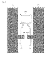
Fig. 1 is a view showing a welding method and a welding structure according to an embodiment of the present invention; -
Fig. 2 is a cross-sectional view taken along line A-B ofFig. 1 ; -
Fig. 3 is a table showing a welding strength; -
Fig. 4 is a view showing an example of a ceramic capacitor and a metal plate welded by the welding method of the present invention; -
Fig. 5 is a view showing a conventional welding method and a welding structure; -
Fig. 6 is a cross sectional view taken along line P-Q ofFig. 5 ; -
Fig. 7 is a cross-sectional view showing another conventional welding method and a welding structure; and -
Fig. 8 is a view showing an example of a ceramic capacitor and a metal plate welded by the conventional welding method. - Hereinafter, preferred embodiments of the present invention will be described with reference to the drawings.
InFigs. 1 to 4 , same reference numerals are denoted for the same or corresponding portions. -
Fig. 1 is a view showing one embodiment of a welding method and a welding structure according to the present invention.
In the figure, 100 denotes a ceramic capacitor, and 21a and 21b denote metal plates (lead frames) for attaching theceramic capacitor 100.
In the present embodiment, a diameter oflead wires ceramic capacitor 100 including thelead wires metal plates
For instance, inFig. 1 , a diameter d of thelead wires ceramic capacitor 100 is 0,5 mm, and a thickness t (seeFig. 2 ) of themetal plates lead wires metal plates - As described above, when joining the lead wire having a diameter of 0.5 mm to the metal plate by resistance welding, a typical thickness is between 0.64 mm and 0.8 mm for the thickness of the metal plate to carry out the welding satisfactorily.
Thus, when the thickness of themetal plates lead wires lead wire 11a and themetal plate 21a, and thelead wire 11b and themetal plate 21b may not be satisfactorily welded. - Thus, in the present embodiment, the following measures are taken to satisfactorily weld the
lead wire 11a and themetal plate 21a, and thelead wire 11b and themetal plate 21b even when the thickness of themetal plates - First, the
metal plates
Specifically, as shown inFig. 1 ,projections metal plates metal plates - In the present embodiment, the
projections lead wires metal plates
For instance, inFig. 1 , the length x of theprojections metal plates - The
ceramic capacitor 100 is then attached to themetal plates Figs. 1 and2. Fig. 2 is a view showing a cross-section taken along line A-B inFig. 1 . - When attaching the
ceramic capacitor 100 to themetal plates lead wire 11a and themetal plate 21a are brought into contact with each other and resistance-welded, and thelead wire 11b and themetal plate 21b are brought into contact with each other and resistance-welded, as shown inFigs. 1 and2 . - Specifically, when carrying out welding on the
lead wire 11a and themetal plate 21a, part of thelead wire 11a and theprojection 22a are brought into contact with each other such that the longitudinal direction (a direction) of thelead wire 11a and the projecting direction (b direction) of theprojection 22a become orthogonal, as shown inFig. 1 .
Thereafter, as shown inFig. 2 , theelectrode 31a is pressure-welded to thelead wire 11a at a predetermined pressurizing force F1 and theelectrode 31c is pressure-welded to theprojection 22a at the predetermined pressurizing force F1 such that theelectrode 31a and theelectrode 31c face each other with thelead wire 11a and theprojection 22a in between. Thus, thelead wire 11a and theprojection 22a are sandwiched with the pressurizing force F1 by theelectrodes electrode 31a serves as a first electrode of the present invention, and theelectrode 31c serves as a second electrode of the present invention. - Similarly, when carrying out welding on the
lead wire 11b and themetal plate 21b, part of thelead wire 11b and theprojection 22b are brought into contact with each other such that the longitudinal direction (a direction) of thelead wire 11b and the projecting direction (b direction) of theprojection 22b become orthogonal (seeFig. 1 ).
Thereafter, theelectrodes 31b is pressure-welded to thelead wire 11b at the predetermined pressurizing force F1 and theelectrode 31d is pressure-welded to theprojection 22b at the predetermined pressurizing force F1 such that theelectrode 31b and theelectrode 31d face each other with thelead wire 11b and theprojection 22b in between (seeFig. 2 ). Thus, thelead wire 11b and theprojection 22b are sandwiched with the pressurizing force F1 by theelectrodes electrode 31b serves as a first electrode of the present invention, and theelectrode 31d serves as a second electrode of the present invention. - A large current is flowed between the
electrodes power supply 41a as soon as thelead wire 11a and theprojection 22a are pressure-welded by theelectrodes electrodes power supply 41b as soon as thelead wire 11b and theprojection 22b are pressure-welded by theelectrodes - In the present embodiment, magnitude of the pressurizing force F1 applied by the
electrodes electrodes
When the current of the same magnitude is flowed, theprojections lead wires electrodes electrodes lead wire 11a and theprojection 22a, and thelead wire 11b and theprojection 22b at the respective contacting surface when a current is flowed between theelectrodes electrodes - In the welding method and the welding structure described above, when the
lead wire 11a and theprojection 22a and thelead wire 11b and theprojection 22b are resistance-welded with the magnitude of the current to flow between theelectrodes electrodes Fig. 3 is obtained for the welding strength by the relevant wending
The welding strength of table 51 is the measurement result obtained by measuring the force required when stripping the weldedlead wire 11a and theprojection 22a, and thelead wire 11b and theprojection 22b, respectively. - In
Fig. 3 , 51a indicates the magnitude (hereinafter referred to as "current flowed amount") of the current flowed between theelectrodes electrodes
Furthermore, 51c indicates the welding strength at the welding place of thelead wire 11a and theprojection 22a, and shows each measurement result of when the current flowedamount 51a and the current flowedtime 51b are respectively changed.
In the present embodiment, the results similar to table 51 are obtained even when thelead wire 11b and theprojection 22b are resistance-welded by theelectrodes - In table 51 of
Fig. 3 , for example, thewelding strength 51c of when a current is flowed between theelectrodes amount 51a as 2.4 kA and the current flowedtime 51b as 20 ms is 10.20 N. That is, the force of 10.20 N is necessary when stripping the weldedlead wire 11a and theprojection 22a.
Similarly, thewelding strength 51c of when a current is flowed between theelectrodes amount 51a as 2.8 kA and the current flowedtime 51b as 40 ms is 46.88 N. That is, the force of 46.88 N is necessary when stripping the weldedlead wire 11a and theprojection 22a. - Each
welding strength 51c in table 51 is the welding strength of when the number of sampling is one, and thus the inventor of the present invention performed a verification on the condition for satisfactorily welding thelead wire 11a and theprojection 22a, that is, a satisfactory combination of the current flowedamount 51a and the current flowedtime 51b in flowing a current between theelectrodes - As a result of performing trial on various combinations, the
lead wire 11a was welded in a state shown with a shadedarea 12a inFig. 4 with the current flowedamount 51a as 2.6 kA and the current flowedtime 51b as 30 ms. Specifically, when confirmed that thelead wire 11a is welded in a state sunk into theprojection 22a, and the weldedlead wire 11a and theprojection 22a are stripped, a tubular nugget was found on theprojection 22a side. - Thus, in the resistance welding, the condition for satisfactorily performing welding on the
lead wire 11a and theprojection 22a in the present embodiment is the portion surrounded by the shaded area in table 51, that is, when the current flowedamount 51a is 2.6 kA and the current flowedtime 51b is 30 ms as thelead wire 11a and theprojection 22a were experimentally proved to be satisfactorily welded without producing a flat part squashed by theelectrode 31a at the welding place of thelead wire 11a. In table 51, the welding strength in this case is 41.38 N. - Thus, in the embodiment described above, the
projections metal plates lead wires lead wire 11a and theprojection 22a are brought into contact with each other and part of thelead wire 11b and theprojection 22b are brought into contact with each other such that the longitudinal direction of thelead wires projections electrodes electrodes projections entire metal platens - Thus only the welding place can be heated in a concentrated manner, and the
lead wire 11a and themetal plate 21a and thelead wire 11b and themetal plate 21b can be respectively satisfactorily welded even when carrying out welding on the lead wire with the metal plate having a thickness of greater than or equal to twice the diameter of the lead wire. - As heat distribution becomes satisfactory, the
lead wire 11a and themetal plate 21a, and thelead wire 11b and themetal plate 21b can be welded, respectively, without excessively melting thelead wires flat parts Fig. 8 . Thus, the formation of the nugget stabilizes in the relevant welding, whereby the welding strength does not lower. - Furthermore, the welding is prevented from extending to the place where welding is unnecessary since the welding place can be confined.
- In the embodiment described above, the formation of projection at the
metal plates metal plates metal plates metal plates - In the present invention, various embodiments other than those described above can be adopted. For instance, the lead wire of the ceramic capacitor is attached to the metal plate in the embodiment described above, but the present invention is not limited thereto, and the lead wire of other electronic parts (e.g., semiconductor) may be attached to the metal plate.
- Furthermore, the lead wire and the metal plate are resistance-welded in the embodiment described above, but the present invention is not limited thereto, and conductive terminals (e.g., metal rod and metal plate) in which the length and the width are different from each other may be resistance-welded.
- In the embodiment described above, the steel wire is used for the lead wire and the copper plate is used for the metal plate, but the present invention is not limited thereto, and the lead wire and the metal plate may be made from a similar material (e.g., iron).
- Furthermore, in the embodiment described above, the projection has a square shape, but the present invention is not limited thereto, and the shape may be such that the strength of the projection is maintained and the length in the direction orthogonal to the longitudinal direction of the metal plate is longer than the width of the longitudinal direction (e.g., semi-ellipse).
- In accordance with one aspect of the present invention, a welding method of conductive terminals for performing resistance welding on a first conductive terminal and a second conductive terminal includes the steps of: bringing the first conductive terminal into contact with a projection formed on the second conductive terminal and projecting in a direction orthogonal to a longitudinal direction of the terminal; and joining a first electrode to the first conductive terminal by pressure welding and joining a second electrode to the projection by pressure welding with the longitudinal direction of the first conductive terminal and the projecting direction of the projection orthogonal to each other, and flowing a current between each electrode to weld the first conductive terminal and the projection at a contacting surface thereof.
- Therefore, the Joule heat generated at the second conductive terminal by flowing a current can be suppressed from diffusing to the entire second conductive terminal when the current is flowed between the first electrode and the second electrode, whereby the first conductive terminal and the second conductive terminal can be satisfactorily welded without arranging the projection even when the thickness of the terminal is thick.
- In the welding method according to the present invention, preferably, a length in the projecting direction of the projection is greater than a width in a direction orthogonal to the projecting direction of the projection and a width of the first conductive terminal, and a width of the projection is less than a length of the first conductive terminal.
- The heat distribution thus becomes satisfactory, and the first conductive terminal and the second conductive terminal can be welded without excessively melting the first conductive terminal, that is, without producing a flat part squashed by the first electrode, and the welding can be carried out at a satisfactory welding strength.
- In the welding method according to the present invention, preferably, a width d (mm) of the first conductive terminal is 0.5 ≤ d ≤ 0.75, and a thickness t (mm) of the second conductive terminal is 1.0 ≤ t ≤ 1.8.
- In the welding method according to the present invention, preferably, a length x (mm) in the projecting direction of the projection is x ≥ 3, and a width y (mm) in a direction orthogonal to the projecting direction of the projection is 1,5 ≤ y ≤ 2.
- In the welding method according to the present invention, the first conductive terminal may be a steel wire having a circular cross-section, and the second conductive terminal may be a copper plate having a flat plate shape.
- Therefore, the welding method can be applied as is to the conventionally used electronic component without using a special material for the conductive terminal to be welded.
- In the welding method according to the present invention, the first electrode may be made of chromium copper, and the second electrode may be made of tungsten.
- Therefore, the first conductive terminal and the second conductive terminal can be equally melted even when the electrical resistivity of the first conductive terminal and the second conductive terminal differ from each other, that is, even when performing welding on the first conductive terminal made of steel wire and the second conductive terminal made of copper plate, and thus the first conductive terminal and the second conductive terminal can be welded without excessively melting the first conductive terminal, that is, without producing the flat part and the welding can be carried out at satisfactory welding strength.
- In accordance with another aspect of the present invention, a welding structure according to the present invention is a welding structure of conductive terminals in which a first conductive terminal and a second conductive terminal are resistance-welded, wherein the second conductive terminal incudes a projection projecting in a direction orthogonal to a longitudinal direction of the terminal, and the first conductive terminal is resistance-welded to the projection with the longitudinal direction of the terminal and a longitudinal direction of the projection orthogonal to each other.
- Thus, the Joule heat generated at the second conductive terminal by flowing a current can be suppressed from diffusing to the entire second conductive terminal when the current is flowed between the first electrode and the second electrode, whereby the first conductive terminal and the second conductive terminal can be satisfactorily welded without arranging the projection even when the thickness of the terminal is thick.
- According to the present invention, the Joule heat generated by flowing a current can be suppressed from diffusing to the entire conductive terminal, whereby the first conductive terminal and the second conductive terminal can be satisfactorily welded without arranging the projection.
Claims (7)
- A welding method of conductive terminals (11a, 11b, 21a, 21b) for performing resistance welding on a first conductive terminal (11a, 11b) and a second conductive terminal (21a, 21b); the method comprising the steps of:bringing the first conductive terminal (11a, 11b) into contact with a projection (22a, 22b) formed on the second conductive terminal (21a, 21b) and projecting in a direction orthogonal to a longitudinal direction of the terminal (21a, 21b); andjoining a first electrode (31a, 31b) to the first conductive terminal (11a, 11b) by pressure welding and joining a second electrode (31c, 31d) to the projection (22a, 22b) by pressure welding with the longitudinal direction of the first conductive terminal (11a, 11b) and the projecting direction of the projection (22a, 22b) orthogonal to each other, and flowing a current between each electrode (31a, 31b, 31c, 31d) to weld the first conductive terminal (11a, 11b) and the projection (22a, 22b) at a contacting surface thereof.
- The welding method of the conductive terminals (11a, 11b, 21a, 21b) according to claim 1, characterized in that a length in the projecting direction of the projection (22a, 22b) is greater than a width in a direction orthogonal to the projecting direction of the projection (22a, 22b) and a width of the first conductive terminal (11a, 11b), and a width of the projection (22a, 22b) is less than a length of the first conductive terminal (11a, 11b).
- The welding method of the conductive terminals (11a, 11b, 21a, 21b) according to claim 1, characterized in that a width d (mm) of the first conductive terminal (11a, 11b) is 0.5 ≤ d ≤ 0.75, and a thickness t (mm) of the second conductive terminal (21a, 21b) is 1.0 ≤ t ≤ 1.8.
- The welding method of the conductive terminals (11a, 11b, 21a, 21b) according to claim 1, characterized in that a length x (mm) in the projecting direction of the projection (22a, 22b) is x ≥ 3, and a width y (mm) in a direction orthogonal to the projecting direction of the projection (22a, 22b) is 1.5 ≤ y ≤ 2.
- The welding method of the conductive terminals (11a, 11b, 21a, 21b) according to claim 1, characterized in that the first conductive terminal (11a, 11b) is a steel wire having a circular cross-section, and the second conductive terminal (21a, 21b) is a copper plate having a flat plate shape.
- The welding method of the conductive terminals (11a, 11b, 21a, 21b) according to claim 5, characterized in that the first electrode (31a, 31b) is made of chromium copper, and the second electrode (31c, 31d) is made of tungsten.
- A welding structure of conductive terminals (11a, 11b, 21a, 21b) in which a first conductive terminal (11a, 11b) and a second conductive terminal (21a, 21b) are resistance-welded, characterized in that
the second conductive terminal (21a, 21b) includes a projection (22a, 22b) projecting in a direction orthogonal to a longitudinal direction of the terminal (21a, 21b), and the first conductive terminal (11a, 11b) is resistance-welded to the projection (22a, 22b) with the longitudinal direction of the terminal (11a, 11b) and a longitudinal direction of the projection (22a, 22b) orthogonal to each other.
Applications Claiming Priority (1)
| Application Number | Priority Date | Filing Date | Title |
|---|---|---|---|
| JP2008185514A JP2010027316A (en) | 2008-07-17 | 2008-07-17 | Welding method and welding structure of conductive terminal |
Publications (1)
| Publication Number | Publication Date |
|---|---|
| EP2145716A1 true EP2145716A1 (en) | 2010-01-20 |
Family
ID=41202880
Family Applications (1)
| Application Number | Title | Priority Date | Filing Date |
|---|---|---|---|
| EP09165431A Withdrawn EP2145716A1 (en) | 2008-07-17 | 2009-07-14 | Welding method and welding structure of conductive terminals |
Country Status (4)
| Country | Link |
|---|---|
| US (1) | US20100012374A1 (en) |
| EP (1) | EP2145716A1 (en) |
| JP (1) | JP2010027316A (en) |
| CN (1) | CN101630647B (en) |
Cited By (1)
| Publication number | Priority date | Publication date | Assignee | Title |
|---|---|---|---|---|
| CN109623079A (en) * | 2019-01-19 | 2019-04-16 | 巨力自动化设备(浙江)有限公司 | Asterism wire bonding picks |
Families Citing this family (2)
| Publication number | Priority date | Publication date | Assignee | Title |
|---|---|---|---|---|
| DE102021117573B4 (en) * | 2021-07-07 | 2023-04-13 | Tdk Electronics Ag | Method of making an electrical connection to an electronic component and a chip assembly |
| CN118136540B (en) * | 2024-05-06 | 2024-09-06 | 深圳中宝新材科技有限公司 | Stress testing method and system for gold wire bonding |
Citations (4)
| Publication number | Priority date | Publication date | Assignee | Title |
|---|---|---|---|---|
| US3315199A (en) * | 1965-08-13 | 1967-04-18 | Gen Electric | Electrical terminal or tap for a strip wound coil and method of making the same |
| JPH02132783A (en) * | 1988-11-11 | 1990-05-22 | Toshiba Corp | Lead connecting method |
| JPH05283139A (en) * | 1992-04-02 | 1993-10-29 | Yazaki Corp | Resistance welding method for different metal terminal |
| EP1453190A1 (en) * | 2003-02-28 | 2004-09-01 | Denso Corporation | Connection between a rectifier and a voltage regulator in a vehicle alternator |
Family Cites Families (6)
| Publication number | Priority date | Publication date | Assignee | Title |
|---|---|---|---|---|
| DE3510370A1 (en) * | 1985-03-22 | 1986-09-25 | kabelmetal electro GmbH, 3000 Hannover | METHOD FOR CONNECTING TWO ELECTRIC LINES |
| US5195682A (en) * | 1992-03-05 | 1993-03-23 | Honeywell Inc. | Method for attaching copper to a ferrous alloy |
| JP3595385B2 (en) * | 1995-08-07 | 2004-12-02 | ナイルス株式会社 | Terminal and lead wire joining structure and terminal and lead wire joining method |
| JPH0963658A (en) * | 1995-08-29 | 1997-03-07 | Yamatake Honeywell Co Ltd | Lead wire connection structure |
| US7339114B2 (en) * | 2002-04-04 | 2008-03-04 | Fujikura Ltd. | Cable, cable connection method and cable welder |
| JP4939899B2 (en) * | 2006-10-30 | 2012-05-30 | オムロンオートモーティブエレクトロニクス株式会社 | Conductive terminal welding method and conductive terminal structure |
-
2008
- 2008-07-17 JP JP2008185514A patent/JP2010027316A/en active Pending
-
2009
- 2009-07-14 EP EP09165431A patent/EP2145716A1/en not_active Withdrawn
- 2009-07-16 US US12/504,253 patent/US20100012374A1/en not_active Abandoned
- 2009-07-17 CN CN2009101607133A patent/CN101630647B/en not_active Expired - Fee Related
Patent Citations (6)
| Publication number | Priority date | Publication date | Assignee | Title |
|---|---|---|---|---|
| US3315199A (en) * | 1965-08-13 | 1967-04-18 | Gen Electric | Electrical terminal or tap for a strip wound coil and method of making the same |
| JPH02132783A (en) * | 1988-11-11 | 1990-05-22 | Toshiba Corp | Lead connecting method |
| JP2666988B2 (en) | 1988-11-11 | 1997-10-22 | 株式会社東芝 | Lead connection method |
| JPH05283139A (en) * | 1992-04-02 | 1993-10-29 | Yazaki Corp | Resistance welding method for different metal terminal |
| JP2747506B2 (en) | 1992-04-02 | 1998-05-06 | 矢崎総業株式会社 | Resistance welding method for dissimilar metal terminals |
| EP1453190A1 (en) * | 2003-02-28 | 2004-09-01 | Denso Corporation | Connection between a rectifier and a voltage regulator in a vehicle alternator |
Cited By (2)
| Publication number | Priority date | Publication date | Assignee | Title |
|---|---|---|---|---|
| CN109623079A (en) * | 2019-01-19 | 2019-04-16 | 巨力自动化设备(浙江)有限公司 | Asterism wire bonding picks |
| CN109623079B (en) * | 2019-01-19 | 2023-09-12 | 巨力自动化设备(浙江)有限公司 | Star point line welding machine |
Also Published As
| Publication number | Publication date |
|---|---|
| CN101630647B (en) | 2011-05-11 |
| CN101630647A (en) | 2010-01-20 |
| JP2010027316A (en) | 2010-02-04 |
| US20100012374A1 (en) | 2010-01-21 |
Similar Documents
| Publication | Publication Date | Title |
|---|---|---|
| CN100566024C (en) | Welding method of conductive terminal and structure of conductive terminal | |
| JP6795879B2 (en) | Resistor and its manufacturing method | |
| KR101818631B1 (en) | Battery and method of manufacturing same | |
| US8368502B2 (en) | Surface-mount current fuse | |
| CN102640324A (en) | Method for producing an electrically conductive connection | |
| KR20080071518A (en) | Projection Welds and Methods for Forming Projection Welds | |
| CN102194620B (en) | Fuse and manufacturing method of the same | |
| EP2145716A1 (en) | Welding method and welding structure of conductive terminals | |
| WO2015111509A1 (en) | Terminal fitting-equipped electrical wire and method for manufacturing same | |
| JP2011243504A (en) | Temperature fuse and method of manufacturing temperature fuse | |
| JP3454055B2 (en) | Connection structure and connection method of insulated wire | |
| KR100820517B1 (en) | Circuit board | |
| US8282432B2 (en) | Weld terminal, switch assembly and methods of attachment | |
| JP2000164093A (en) | Thermal fuse and manufacturing method thereof | |
| JP2009231559A (en) | Method of attaching resistor | |
| CN109285634B (en) | Method for integrally connecting metal core wires of flat cable and flat cable | |
| CN105284023A (en) | Terminal bonding structure of electric wire and electrode for resistance welding | |
| CN117174679A (en) | Connection components, fusion weld connections, metal component manufacturing methods, connection kits and methods of connecting metal components to leads | |
| JP4224050B2 (en) | Heater chip thermocouple mounting structure and thermocouple mounting method | |
| JPS60210383A (en) | Fine wire joining method | |
| JP2014135190A (en) | Thermal fuse and method for manufacturing the same | |
| JPH0970672A (en) | Welding method for dissimilar plates | |
| JPH07254771A (en) | High current printed circuit board manufacturing method | |
| KR100506491B1 (en) | A superprecision welding terminal thereof | |
| JP2025097144A (en) | Method for manufacturing a conductor connection structure |
Legal Events
| Date | Code | Title | Description |
|---|---|---|---|
| PUAI | Public reference made under article 153(3) epc to a published international application that has entered the european phase |
Free format text: ORIGINAL CODE: 0009012 |
|
| AK | Designated contracting states |
Kind code of ref document: A1 Designated state(s): AT BE BG CH CY CZ DE DK EE ES FI FR GB GR HR HU IE IS IT LI LT LU LV MC MK MT NL NO PL PT RO SE SI SK SM TR |
|
| AX | Request for extension of the european patent |
Extension state: AL BA RS |
|
| 17P | Request for examination filed |
Effective date: 20100719 |
|
| RAP1 | Party data changed (applicant data changed or rights of an application transferred) |
Owner name: OMRON AUTOMOTIVE ELECTRONICS CO., LTD. |
|
| GRAP | Despatch of communication of intention to grant a patent |
Free format text: ORIGINAL CODE: EPIDOSNIGR1 |
|
| GRAJ | Information related to disapproval of communication of intention to grant by the applicant or resumption of examination proceedings by the epo deleted |
Free format text: ORIGINAL CODE: EPIDOSDIGR1 |
|
| GRAP | Despatch of communication of intention to grant a patent |
Free format text: ORIGINAL CODE: EPIDOSNIGR1 |
|
| 17Q | First examination report despatched |
Effective date: 20130204 |
|
| STAA | Information on the status of an ep patent application or granted ep patent |
Free format text: STATUS: THE APPLICATION IS DEEMED TO BE WITHDRAWN |
|
| 18D | Application deemed to be withdrawn |
Effective date: 20150203 |