EP2144098A1 - Guide d'onde planaire à base de cristal photonique comportant un adaptateur de modes guidés et système optique comportant le guide d'onde couplé avec une fibre optique - Google Patents
Guide d'onde planaire à base de cristal photonique comportant un adaptateur de modes guidés et système optique comportant le guide d'onde couplé avec une fibre optique Download PDFInfo
- Publication number
- EP2144098A1 EP2144098A1 EP09164816A EP09164816A EP2144098A1 EP 2144098 A1 EP2144098 A1 EP 2144098A1 EP 09164816 A EP09164816 A EP 09164816A EP 09164816 A EP09164816 A EP 09164816A EP 2144098 A1 EP2144098 A1 EP 2144098A1
- Authority
- EP
- European Patent Office
- Prior art keywords
- photonic crystal
- membrane
- circuit according
- guide
- nanometers
- Prior art date
- Legal status (The legal status is an assumption and is not a legal conclusion. Google has not performed a legal analysis and makes no representation as to the accuracy of the status listed.)
- Granted
Links
Images




Classifications
-
- G—PHYSICS
- G02—OPTICS
- G02B—OPTICAL ELEMENTS, SYSTEMS OR APPARATUS
- G02B6/00—Light guides; Structural details of arrangements comprising light guides and other optical elements, e.g. couplings
- G02B6/10—Light guides; Structural details of arrangements comprising light guides and other optical elements, e.g. couplings of the optical waveguide type
- G02B6/12—Light guides; Structural details of arrangements comprising light guides and other optical elements, e.g. couplings of the optical waveguide type of the integrated circuit kind
- G02B6/122—Basic optical elements, e.g. light-guiding paths
- G02B6/1225—Basic optical elements, e.g. light-guiding paths comprising photonic band-gap structures or photonic lattices
-
- B—PERFORMING OPERATIONS; TRANSPORTING
- B82—NANOTECHNOLOGY
- B82Y—SPECIFIC USES OR APPLICATIONS OF NANOSTRUCTURES; MEASUREMENT OR ANALYSIS OF NANOSTRUCTURES; MANUFACTURE OR TREATMENT OF NANOSTRUCTURES
- B82Y20/00—Nanooptics, e.g. quantum optics or photonic crystals
-
- G—PHYSICS
- G02—OPTICS
- G02B—OPTICAL ELEMENTS, SYSTEMS OR APPARATUS
- G02B6/00—Light guides; Structural details of arrangements comprising light guides and other optical elements, e.g. couplings
- G02B6/10—Light guides; Structural details of arrangements comprising light guides and other optical elements, e.g. couplings of the optical waveguide type
- G02B6/12—Light guides; Structural details of arrangements comprising light guides and other optical elements, e.g. couplings of the optical waveguide type of the integrated circuit kind
- G02B6/122—Basic optical elements, e.g. light-guiding paths
- G02B6/1228—Tapered waveguides, e.g. integrated spot-size transformers
-
- G—PHYSICS
- G02—OPTICS
- G02B—OPTICAL ELEMENTS, SYSTEMS OR APPARATUS
- G02B6/00—Light guides; Structural details of arrangements comprising light guides and other optical elements, e.g. couplings
- G02B6/24—Coupling light guides
- G02B6/26—Optical coupling means
- G02B6/30—Optical coupling means for use between fibre and thin-film device
- G02B6/305—Optical coupling means for use between fibre and thin-film device and having an integrated mode-size expanding section, e.g. tapered waveguide
-
- G—PHYSICS
- G02—OPTICS
- G02B—OPTICAL ELEMENTS, SYSTEMS OR APPARATUS
- G02B6/00—Light guides; Structural details of arrangements comprising light guides and other optical elements, e.g. couplings
- G02B6/10—Light guides; Structural details of arrangements comprising light guides and other optical elements, e.g. couplings of the optical waveguide type
- G02B6/12—Light guides; Structural details of arrangements comprising light guides and other optical elements, e.g. couplings of the optical waveguide type of the integrated circuit kind
- G02B2006/12166—Manufacturing methods
- G02B2006/12176—Etching
-
- G—PHYSICS
- G02—OPTICS
- G02B—OPTICAL ELEMENTS, SYSTEMS OR APPARATUS
- G02B6/00—Light guides; Structural details of arrangements comprising light guides and other optical elements, e.g. couplings
- G02B6/10—Light guides; Structural details of arrangements comprising light guides and other optical elements, e.g. couplings of the optical waveguide type
- G02B6/12—Light guides; Structural details of arrangements comprising light guides and other optical elements, e.g. couplings of the optical waveguide type of the integrated circuit kind
- G02B2006/12166—Manufacturing methods
- G02B2006/12195—Tapering
Definitions
- the field of the invention is that of photonic crystal circuits that provide original functions in the field of photonics: all-optical signal processing, optical sampling, delay line, filtering, chemical sensor, source of single photons.
- optical devices of very small size and very low consumption, particularly sought for applications in the field of quantum communications (cryptography, calculation, ..) or for the so-called “extreme" integration.
- photonic crystals are structures whose dielectric index varies periodically at the wavelength scale over one or more directions of space.
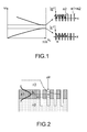
- the figure 1 illustrates the intensity of the electric field of an electromagnetic wave propagating in this type of structure and shows the dispersion diagram of a structure of period a in the first Brillouin zone; the wave vector k is in the range 0 ⁇ k ⁇ / a.
- artificially structure materials for example semiconductors, to take advantage of diffraction effects, thereby enabling the development of passive and active optical functions necessary, for example, for optical fiber telecommunications networks.
- one of the major attractions of these structures is based on the controlled insertion of defects within the crystal. These defects can generate states at bandgap frequencies of the crystal and thus allow a propagating electromagnetic field for these frequencies. A control of the propagation of light within the crystal and at the wavelength scale is then possible via these defects. The use of these structures thus opens the way to the miniaturization of components in integrated optics.
- a very thin layer is thus isolated, thus constituting a membrane that can typically have a thickness h of the order of 150 nanometers to 300 nanometers for applications targeting the spectral range between about 1 micron and 1.6 microns.
- h is between 0.1 and 0.3 times the wavelength.
- the material used can typically be silicon or a semiconductor material based on elements of columns III and V of the Mendeleyev periodic table ("III-V" semiconductors, for example GaAs, AlGaAs, GaInP, InP, AlGaAsP, etc. .).
- Materials that can also be envisaged are the semiconductors of family II-VI (for example ZnO) as well as SiN.
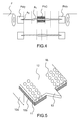
- a waveguide is created with a strong optical index variation as illustrated in FIG. figure 2 .
- the wave propagation speed and the dispersion of the guided modes can be adjusted by varying the size of the patterns.
- This silicon Si element is formed on the surface of an SiO 2 oxide layer and embedded in the polymer referenced Poly. It is thus possible to use it as an adapter.
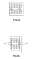
- the Figures 3a and 3b illustrate this adapter element and the figure 4 represents the solution recommended in this article which consists in making a three-stage adaptation between the guided modes of the fibers F and those from the photonic crystal PhC.
- a first element A 1 couples the mode of the photonic crystal to that of a suspended ribbon guide. A transition is then made to a ribbon guide resting on the low index sacrificial layer. Finally, a last element A 2 adapts the optical mode of the latter to that of the optical fiber F.
- the adapter element on the surface of the SiO 2 layer is then in a heterogeneous environment. It rests on a substrate while its upper surface is not in contact with the same type of material. This property creates an asymmetry in the confinement of optical modes.
- the present invention proposes a mode adapter that transforms the mode of the photonic crystal into a propagative mode in Gaussian free space with a numerical aperture such that it allows efficient coupling with an optical fiber. through a standard adapted optics (micro-lens, lentil fiber, GRIN lens, micro-sphere).
- the invention relates to a photonic crystal circuit comprising a guide made in a dielectric material membrane and a mode adapter coupled to said guide characterized in that the membrane comprises a central tip constituting the mode adapter having a section gradient terminating said guide, said tip being suspended so as to allow the propagation of modes symmetrically.
- the tip protrudes from the cleavage plane of the substrate in order to avoid parasitic reflections on the latter.
- the membrane is made of silicon.
- the membrane is of type III-V material such as GaAs, GaAlAs, GaInP, InP, GaInAsP.
- the thickness of the membrane is between about 100 nanometers and 300 nanometers for applications in the range of 900nm to 1600nm.
- the photonic crystal comprises units having a periodicity of the order of a few hundred nanometers.
- the photonic crystal patterns are holes having radii of the order of 120 to 130 nanometers depending on the target operating wavelength.
- the operation of producing a groove is carried out over a width of the order of a hundred nanometers.
- the invention further relates to an optical system comprising a photonic crystal circuit according to the invention, an adaptive optics and an optical fiber.
- the adaptive optics is of the micro-lens or GRIN type (graded index) type.
- a photonic crystal circuit capable of being coupled to a standard optical fiber and which minimizes losses during the transmission of photons from the optical crystal into the fiber.
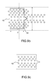
- This circuit includes as illustrated in figure 5 , a membrane 11 made of a thin layer of semiconductor material within which are introduced periodic patterns that can typically be holes.
- a guide 12 is made at the level of this membrane and materialized by an absence of periodic patterns.
- This membrane is developed on the surface of a substrate 10a which may advantageously comprise a so-called sacrificial 10b on which are formed the periodic patterns Mi shaped holes formed within the membrane 11.
- the photon guide is extended by an adapter element 13 having a section gradient without periodic patterns so as to create a mode adaptation at the output of the guide.
- An additional advantage of the photonic crystal circuit of the present invention is the strong reduction of parasitic reflections at the input / output facets, eliminating the need for specific antireflection treatments which are required with abrupt fracture of the output of a photonic crystal circuit of the prior art.
- the radiation patterns of these structures are illustrated in figure 8b and 8c and show a better directivity with adapter element.
- the dashed line curves 8b 1 and 8c 1 are relative to the sagittal plane, the curves in bold lines 8b 2 and 8c 2 are relative to the azimuthal plane in the polar coordinate coordinate system illustrated in FIG. figure 8a .
- the appearance of a quasi-circular mode reflects the improvement of the coupling in the case of the structure with tip ensuring the adaptation function.
- One of the major advantages of the present invention also lies in the simplicity of development of the tip termination guide which can be performed at the same time as the other technological steps that manufacture the photonic crystal circuit.
- a stack of a sacrificial layer 10b and a layer of semiconductor material 11 providing the membrane function, in which holes are made, are produced. locally Mi, while retaining a patternless area dedicated to the guide 12 as illustrated in figure 9a .
- the distance d represented on the figure 9b typically can be of the order of 10 .mu.m to 40 .mu.m; this value can be reduced according to the cleavage tolerances as well as the alignment accuracy of the patterns with respect to the crystalline plane of the semiconductor.
- cleavage step is used to isolate the tip at the edge of the guide as shown in FIG. Figure 9c .
- the photonic crystal circuit thus produced can advantageously be integrated into an optical system.
- the tip of said circuit is coupled to an optical fiber whose end may advantageously be provided with a lens that can typically have a focal length of the order of 10 to 20 microns.
- the figure 10 illustrates an example of application in which the photonic crystal equipped with its adapter portion provides the function of coupler is particularly interesting.
- couplers C 1 , C 2 and C 3 are used to couple the input signals Se and control Sc to guides arranged to achieve an interferometer architecture.
- the guides are made within photonic crystals of membrane type, by modification of the periodic structure, typically performed by lack of patterns.
- the device also includes photodetectors PD1 and PD2 for selecting signals resulting from interference of the input and control signals and for sampling the information carrying signal.
- the overall size of such a device can be extremely compact, the dimension d can be of the order of a few millimeters.
Landscapes
- Physics & Mathematics (AREA)
- Engineering & Computer Science (AREA)
- Optics & Photonics (AREA)
- General Physics & Mathematics (AREA)
- Chemical & Material Sciences (AREA)
- Microelectronics & Electronic Packaging (AREA)
- Nanotechnology (AREA)
- Life Sciences & Earth Sciences (AREA)
- Biophysics (AREA)
- Crystallography & Structural Chemistry (AREA)
- Power Engineering (AREA)
- Optical Integrated Circuits (AREA)
- Optical Couplings Of Light Guides (AREA)
Abstract
Description
- Le domaine de l'invention est celui des circuits à cristaux photoniques qui apportent des fonctions originales dans le domaine de la photonique : traitement tout-optique du signal, échantillonnage optique, ligne à retard, filtrage, capteur chimique, source de photons uniques.
- Il s'agit de dispositifs optiques de très petite taille et de très faible consommation, particulièrement recherchés pour des applications dans le domaine des communications quantiques (cryptographie, calcul,..) ou pour l'intégration dite « extrême ».
- De manière générale, les cristaux photoniques sont des structures dont l'indice diélectrique varie de manière périodique à l'échelle de la longueur d'onde, sur une ou plusieurs directions de l'espace. La
figure 1 illustre l'intensité du champ électrique d'une onde électromagnétique se propageant dans ce type de structure et montre le diagramme de dispersion d'une structure de période a dans la première zone de Brillouin ; le vecteur d'onde k est compris dans l'intervalle 0 < k < π / a. On sait structurer artificiellement des matériaux par exemple semiconducteurs pour mettre à profit les effets de diffraction permettant par la même d'élaborer des fonctions optiques passives et actives nécessaires par exemple aux réseaux de télécommunications sur fibre optique. - Par ailleurs un des attraits majeurs de ces structures reposent sur l'insertion contrôlée de défauts au sein du cristal. Ces défauts peuvent générer des états aux fréquences de bande interdite du cristal et ainsi permettre un champ électromagnétique propagatif pour ces fréquences. Un contrôle de la propagation de la lumière au sein du cristal et à l'échelle de la longueur d'onde est alors envisageable via ces défauts. L'utilisation de ces structures ouvre ainsi la voie à la miniaturisation des composants en optique intégrée.
- Par rapport aux structures cristallines en trois dimensions, il a été montré qu'une structure en deux dimensions pouvait être particulièrement intéressante. On réalise dans ce cas, des cristaux dans une fine couche guidante semiconductrice ce qui permet un meilleur contrôle et une technologie plus aisée de réalisation compatible des technologies classiques de microélectronique.
- On isole une couche très fine constituant ainsi une membrane pouvant typiquement présenter une épaisseur h de l'ordre de 150 nanomètres à 300 nanomètres pour les applications visant le domaine spectral entre environ 1 micron et 1.6 microns. Par une simple loi d'échelle, cette épaisseur est ajustée pour étendre l'application à d'autres domaines spectraux. La loi est la suivante : h est compris entre 0.1 et 0.3 fois la longueur d'onde. Le matériau utilisé peut typiquement être du silicium ou un matériau semiconducteur à base d'éléments des colonnes III et V de la table périodique de Mendeleyev (semiconducteurs « III-V », par exemple GaAs, AlGaAs, GaInP, InP, AlGaAsP,...).
- Des matériaux envisageables également sont les semiconducteurs de la famille II-VI (par exemple le ZnO) ainsi que le SiN.
- On crée au sein de ces membranes un guide d'onde avec une forte variation d'indice optique comme illustré en
figure 2 . On peut notamment régler la vitesse de propagation des ondes et la dispersion des modes guidés en faisant varier la taille des motifs. - En outre, ces dispositifs sont extrêmement compacts et peuvent être facilement intégrés. Cela implique une faible consommation, un poids et un volume très réduits, ce qui les rend très attrayants pour les applications embarquées. Cependant, la connexion avec une fibre est un point délicat et il n'existe pas à l'heure actuelle de solution simple et peu coûteuse permettant de répondre à ce problème majeur.
- En effet il convient de réaliser une adaptation entre le mode guidé d'une fibre optique, dont la taille est typiquement de l'ordre de quelques centaines de microns carré (typiquement de l'ordre de 10µm de diamètre), avec celui d'un guide d'onde réalisé au sein d'un cristal photonique capable de confiner des modes dans des sections d'environ 0,2 *0,3 µm2.
- Il a notamment été proposé par des chercheurs d'IBM : Sharee J.McNab, Nikolaj Moll and Yurii A.Vlasov « Ultra-low loss photonic integrated circuit with membrane-type photonic crystal waveguides », OPTICS EXPRESS 2927, 3 November 2003/Vol 11, No.22, une technologie définissant un élément adjacent au cristal photonique et de section variable.
- Cet élément en silicium Si est réalisé à la surface d'une couche d'oxyde SiO2 et noyé dans du polymère référencé Poly. Il est ainsi possible de l'utiliser en tant qu'adaptateur. Les
figures 3a et 3b illustrent cet élément adaptateur et lafigure 4 représente la solution préconisée dans cet article qui consiste à faire une adaptation à trois étages entre les modes guidés des fibres F et ceux issus du cristal photonique PhC. - Selon cette technologie, un premier élément A1 couple le mode du cristal photonique à celui d'un guide ruban suspendu. Une transition s'effectue alors vers un guide ruban reposant sur la couche sacrificielle à basse indice. Enfin un dernier élément A2 adapte le mode optique de ce dernier à celui de la fibre optique F.
- Les inconvénients d'une telle solution résident notamment dans :
- la complexité de la conception (deux adaptateurs de mode),
- la complexité de la réalisation (addition de plusieurs étapes technologiques et inclusion d'un matériau supplémentaire : polymère),
- les réflexions parasites pouvant apparaître à la transition entre le ruban suspendu et le ruban reposant sur le diélectrique (en particulier si celui-ci n'est pas bas indice),
- les réflexions parasites sur le substrat pouvant apparaître et dues à la divergence, même faible, du faisceau,
- la précision de clivage nécessaire pour éviter les précédentes réflexions,
- les effets de proximité durant la lithographie électronique provoqués par le changement de géométrie.
- Par ailleurs, cette solution est réalisable sur un substrat de SiO2 mais est difficilement applicable sur d'autres matériaux car la partie du guide en ruban doit être maintenue par un substrat à faible indice.
- L'élément adaptateur à la surface de la couche de SiO2 se trouve alors dans un environnement hétérogène. Il repose sur un substrat alors que sa surface supérieure n'est pas en contact avec le même type de matériau. Cette propriété crée une dissymétrie au niveau du confinement des modes optiques.
- Il a été aussi proposé par une équipe d'université Japonaise : N. Ikeda, H. Kawashima, Y. Sugimoto, T. Hasama, K. Asakawa, H. lshikawa « Coupling characteristic of micro planar lens for 2D photonic crystal waveguides » Conference Proceedings of IPRM (International Conference on Indium Phosphide and Related Materials) May 2007, une technologie définissant une lentille planaire placée à la terminaison d'un guide d'onde en cristal photonique. Cet élément, réalisé en GaAlAs est utilisé pour diminuer les pertes de couplage et les tolérances d'alignement tout en réduisant les réflexions parasites Fabry-Perot. Le problème principal de cette solution réside dans le fait que le faisceau rayonné n'est pas circulaire de part les facteurs géométriques de la micro-lentille ; cette technique ne permet pas de réduire la divergence dans le plan vertical.
- Pour résoudre ce type de problème, la présente invention propose un adaptateur de mode qui transforme le mode du cristal photonique en un mode propagatif dans l'espace libre de type Gaussien avec une ouverture numérique telle qu'elle permette un couplage efficace avec une fibre optique au travers d'une optique adaptée standard (micro-lentille, fibre lentillée, lentille GRIN, micro-sphère).
- Plus précisément l'invention a pour objet un circuit à cristal photonique comportant un guide réalisé dans une membrane de matériau diélectrique et un adaptateur de mode couplé audit guide caractérisé en ce que la membrane comporte une pointe centrale constitutive de l'adaptateur de mode présentant un gradient de section en terminaison dudit guide, ladite pointe étant suspendue de manière à permettre la propagation de modes de manière symétrique.
- Selon une variante la pointe dépasse du plan de clivage du substrat afin d'éviter les réflexions parasites sur celui-ci.
- Selon une variante de l'invention, la membrane est en silicium.
- Selon une variante de l'invention, la membrane est en matériau de type III-V tel que GaAs, GaAlAs, GaInP, InP, GaInAsP.
- Selon une variante de l'invention, l'épaisseur de la membrane est comprise entre environ 100 nanomètres et 300 nanomètres pour des applications dans le domaine de 900nm à 1600nm.
- Selon une variante de l'invention, le cristal photonique comporte des motifs présentant une périodicité de l'ordre de quelques centaines de nanomètres.
- Selon une variante de l'invention, les motifs du cristal photonique sont des trous présentant des rayons de l'ordre de 120 à 130 nanomètres suivant la longueur d'onde de fonctionnement visée.
- L'invention a aussi pour objet un procédé de fabrication d'un circuit à cristal photonique selon l'invention, caractérisé en ce qu'il comporte les étapes suivantes :
- la réalisation d'un sillon à la surface de la membrane simultanément à la définition du cristal photonique;
- une opération d'attaque chimique de la couche sacrificielle sous-gravant à la fois la pointe de couplage et les structures en cristal photonique ;
- une opération de clivage permettant de libérer la pointe constitutive de l'adaptateur au niveau du sillon préalablement réalisé.
- Selon une variante de l'invention, l'opération de réalisation d'un sillon est effectuée sur une largeur de l'ordre d'une centaine de nanomètres.
- L'invention a encore pour objet un système optique comportant un circuit à cristal photonique selon l'invention, une optique adaptative et une fibre optique.
- Selon une variante de l'invention, l'optique adaptative est de type micro-lentille ou lentille de type GRIN (graded index).
- L'invention sera mieux comprise et d'autres avantages apparaîtront à la lecture de la description qui va suivre donnée à titre non limitatif et grâce aux figures annexées parmi lesquelles :
- la
figure 1 illustre l'intensité du champ électrique d'une onde électromagnétique se propageant dans ce type de structure et montre le diagramme de dispersion d'une structure de période a dans la première zone de Brillouin pour laquelle le vecteur d'onde k est compris dans l'intervalle 0 < k < π / a ; - la
figure 2 illustre une structure bidimensionnelle de cristal photonique comportant un guide d'onde ; - les
figures 3a et 3b illustrent des vues en perspective d'un élément adaptateur de mode selon l'art antérieur et en contact avec un substrat ; - la
figure 4 illustre un exemple de système optique intégrant des adaptateurs tels que ceux illustrés enfigures 3a et 3b ; - la
figure 5 illustre un exemple de circuit à cristal photonique selon l'invention ; - les
figures 6a et 6b illustrent des exemples de structures de guide en cristal photonique respectivement sans pointe et avec double pointe ; - la
figure 7 illustre la transmission normalisée d'une section de guide pour les structures représentées enfigures 6a et 6b ; - les
figures 8b et 8c illustrent les diagrammes de rayonnement dans le plan sagittal et dans le plan azimutal pour les structures représentées enfigures 6a et 6b dans le repère de coordonnées polaires illustré enfigure 8a ; - les
figures 9a à 9c illustrent les différentes étapes d'un exemple de procédé de fabrication d'un circuit à cristal photonique selon l'invention ; - la
figure 10 illustre un circuit à cristal photonique complexe avec des entrées-sorties basées sur la présente invention. - Selon l'invention, il est proposé un circuit à cristal photonique capable d'être couplé à une fibre optique standard et qui minimise les pertes lors de la transmission de photons depuis le cristal optique jusque dans la fibre.
- Ce circuit comprend comme illustré en
figure 5 , une membrane 11 constituée d'une fine couche de matériau semiconducteur au sein de laquelle sont introduits des motifs périodiques pouvant typiquement être des trous. Un guide 12 est réalisé au niveau de cette membrane et matérialisé par une absence de motifs périodiques. Cette membrane est élaborée à la surface d'un substrat 10a qui peut comprendre avantageusement une couche dite sacrificielle 10b sur laquelle sont réalisés les motifs périodiques Mi en forme de trous réalisés au sein de la membrane 11. - Selon l'invention, le guide de photons est prolongé par un élément adaptateur 13 présentant un gradient de section sans motifs périodiques de manière à créer en sortie de guide une adaptation de mode.
- Un avantage supplémentaire du circuit à cristal photonique de la présente invention réside dans la forte réduction des réflexions parasites aux facettes d'entrée/sortie, ce qui élimine la nécessité de traitement anti-reflets spécifiques qui sont nécessaires avec une rupture abrupte de la face de sortie d'un circuit à cristal photonique de l'art connu.
- Des études ont permis de comparer la transmission normalisée d'une section de guide en cristal photonique avec et sans coupleur et mettent en évidence la suppression de réflexions parasites sur les terminaisons. A titre d'exemple les structures des
figures 6a et 6b ont été évaluées en terme de transmission représentées sur lafigure 7 . - Les diagrammes de rayonnement de ces structures sont illustrés en
figure 8b et 8c et font apparaître une meilleure directivité avec élément adaptateur. Les courbes en trait pointillés 8b1 et 8c1 sont relatives au plan sagittal, les courbes en traits gras 8b2 et 8c2 sont relatives au plan azimutal dans le repère de coordonnées polaires illustré enfigure 8a . - L'apparition d'un mode quasi-circulaire traduit l'amélioration du couplage dans le cas de la structure avec pointe assurant la fonction d'adaptation.
- Un des intérêts majeurs de la présente invention réside également dans la simplicité d'élaboration de la pointe en terminaison de guide qui peut être réalisée en même temps que les autres étapes technologiques que celles de fabrication du circuit à cristal photonique.
- Nous allons décrire ci-après un exemple de circuit à cristal photonique selon l'invention et notamment à l'aide des
figures 9a à 9c . - On réalise à la surface d'un substrat 10a, un empilement d'une couche sacrificielle 10b et d'une couche en matériau semiconducteur 11 assurant la fonction de membrane, dans laquelle on réalise des trous périodiques localement Mi, tout en conservant une zone sans motifs dédiée au guide 12 comme illustré en
figure 9a . - Selon une variante illustrée en
figure 9b , on peut réaliser simultanément un sillon Sil en même temps que les trous, ledit sillon pouvant typiquement présenter une largeur d'environ 100 nm , la distance d représentée sur lafigure 9b pouvant typiquement être de l'ordre de 10µm à 40µm ; cette valeur pouvant-être réduite selon les tolérances de clivage ainsi que la précision d'alignement des motifs par rapport au plan cristallin du semiconducteur. - On procède alors à une opération d'attaque chimique de la couche sacrificielle, permettant de dégager la partie inférieure de la pointe, permettant ainsi de définir l'élément adaptateur suspendu qui présente ainsi une symétrie parfaite entre ses faces inférieure et supérieure.
- On procède enfin à une étape de clivage permettant d'isoler la pointe en bordure de guide comme illustré en
figure 9c . - Le circuit à cristal photonique ainsi élaboré peut avantageusement être intégré dans un système optique. La pointe dudit circuit est couplée à une fibre optique dont une extrémité peut avantageusement être munie d'une lentille pouvant typiquement présenter une distance focale de l'ordre de 10 à 20 µm.
- La
figure 10 illustre un exemple d'application dans laquelle le cristal photonique équipé de sa partie adaptatrice assure la fonction de coupleur s'avère particulièrement intéressant. - Il s'agit d'un circuit à cristal photonique complexe avec des entrées-sorties basées sur la présente invention. A partir d'une porteuse ou signal d'entrée émettant un signal à la longueur d'onde λs, il est possible de faire interférer ladite onde signal avec une onde optique de commande à la longueur d'onde λc pour adresser un paquet d'informations de signaux optiques et générer un signal optique de sortie Ss.
- Ainsi, des cristaux photoniques et leur pointe adaptatrice, dénommés coupleurs C1, C2 et C3 permettent de coupler des signaux d'entrée Se et de commande Sc à des guides agencés de manière à réaliser une architecture d'interféromètre. Les guides sont réalisés au sein de cristaux photoniques de type membrane, par modification de la structure périodique, typiquement réalisée par absence de motifs.
- Le dispositif comporte également des photodétecteurs PD1 et PD2, pour sélectionner des signaux résultant des interférences des signaux d'entrée et de commande et permettant d'échantillonner le signal porteur d'informations.
- Typiquement, l'ensemble de l'encombrement d'un tel dispositif peut être extrêmement compact, la dimension d pouvant être de l'ordre de quelques millimètres.
Claims (10)
- Circuit à cristal photonique comportant un guide (12) réalisé dans une membrane (11) de cristal photonique à la surface d'un substrat (10a) et un adaptateur (13) de mode couplé audit guide caractérisé en ce que la membrane comporte une pointe centrale constitutive de l'adaptateur de mode présentant un gradient de section en terminaison dudit guide, ladite pointe étant suspendue de manière à permettre la propagation de modes de manière symétrique.
- Circuit à cristal photonique selon la revendication 1, caractérisé en ce que la membrane est en silicium.
- Circuit à cristal photonique selon la revendication 1, caractérisé en ce que la membrane est en matériau de type III-V tel que GaAs, GaAlAs, GaInP, ou InP, GaInAsP.
- Circuit à cristal photonique selon l'une des revendications 1 à 3, caractérisé en ce que l'épaisseur de la membrane est comprise entre environ 100 nanomètres et 300 nanomètres.
- Circuit à cristal photonique selon l'une des revendications 1 à 4, caractérisé en ce que le cristal photonique comporte des motifs présentant une périodicité de l'ordre de quelques centaines de nanomètres.
- Circuit à cristal photonique selon l'une des revendications 1 à 5, caractérisé en ce que les motifs du cristal photoniques sont des trous présentant des rayons de l'ordre de 120 à 130 nanomètres.
- Procédé de fabrication d'un circuit à cristal photonique selon l'une des revendications 1 à 6, caractérisé en ce qu'il comporte les étapes suivantes :- la réalisation d'un sillon à la surface de la membrane;- une opération d'attaque de la couche sacrificielle (10b)- une opération de clivage permettant de dégager la pointe constitutive de l'adaptateur à partir du sillon préalablement réalisé ;
- Procédé de fabrication d'un circuit photonique selon la revendication 7, caractérisé en ce que l'opération de réalisation d'un sillon est effectuée sur une largeur de l'ordre d'une centaine de nanomètres.
- Système optique comportant un circuit photonique selon l'une des revendications 1 à 6, une optique adaptative et une fibre optique.
- Système optique selon la revendication 9, caractérisé en ce que l'optique adaptative est de type micro-lentille ou lentille de type GRIN.
Applications Claiming Priority (1)
| Application Number | Priority Date | Filing Date | Title |
|---|---|---|---|
| FR0803987A FR2933780B1 (fr) | 2008-07-11 | 2008-07-11 | Circuit a cristal photonique comportant un adaptateur de modes guides et systeme optique comportant ledit circuit couple avec une fibre optique |
Publications (2)
| Publication Number | Publication Date |
|---|---|
| EP2144098A1 true EP2144098A1 (fr) | 2010-01-13 |
| EP2144098B1 EP2144098B1 (fr) | 2011-10-12 |
Family
ID=40428320
Family Applications (1)
| Application Number | Title | Priority Date | Filing Date |
|---|---|---|---|
| EP09164816A Active EP2144098B1 (fr) | 2008-07-11 | 2009-07-07 | Guide d'onde planaire à base de cristal photonique comportant un adaptateur de modes guidés et système optique comportant le guide d'onde couplé avec une fibre optique |
Country Status (4)
| Country | Link |
|---|---|
| US (1) | US8019186B2 (fr) |
| EP (1) | EP2144098B1 (fr) |
| AT (1) | ATE528672T1 (fr) |
| FR (1) | FR2933780B1 (fr) |
Families Citing this family (2)
| Publication number | Priority date | Publication date | Assignee | Title |
|---|---|---|---|---|
| FR2933780B1 (fr) * | 2008-07-11 | 2010-12-17 | Thales Sa | Circuit a cristal photonique comportant un adaptateur de modes guides et systeme optique comportant ledit circuit couple avec une fibre optique |
| JP2017520791A (ja) * | 2014-06-16 | 2017-07-27 | ユニバーシティ オブ コペンハーゲン | 映進面対称導波管を使用する効率的なスピン光子インターフェース |
Citations (2)
| Publication number | Priority date | Publication date | Assignee | Title |
|---|---|---|---|---|
| US20060039649A1 (en) * | 2003-03-14 | 2006-02-23 | Nec Corporation | Method for incidence of light into a photonic crystal optical waveguide and structure thereof |
| US20080089640A1 (en) * | 2006-10-16 | 2008-04-17 | Beausoleil Raymond G | Photonic-based interconnects for interconnecting multiple integrated circuits |
Family Cites Families (7)
| Publication number | Priority date | Publication date | Assignee | Title |
|---|---|---|---|---|
| US6711200B1 (en) * | 1999-09-07 | 2004-03-23 | California Institute Of Technology | Tuneable photonic crystal lasers and a method of fabricating the same |
| AU2003253915A1 (en) * | 2002-07-12 | 2004-02-02 | Massachusetts Institute Of Technology | Reconfigurable microphotonics devices via deformable membrane platform |
| US7157296B2 (en) * | 2003-04-22 | 2007-01-02 | University Of Delaware | Etchless fabrication of planar photonic crystal structures in high refractive index material |
| US7206488B1 (en) * | 2004-09-22 | 2007-04-17 | The Board Of Trustees Of The Leland Stanford Junior University | Coupled photonic crystal resonator array arrangements and applications |
| US7289221B2 (en) * | 2004-09-27 | 2007-10-30 | Hewlett-Packard Development Company, L.P. | Mach Zehnder photonic crystal sensors and methods |
| FR2884916B1 (fr) * | 2005-04-25 | 2007-06-22 | Commissariat Energie Atomique | Detecteur optique ultrasensible a grande resolution temporelle, utilisant un plasmon de surface |
| FR2933780B1 (fr) * | 2008-07-11 | 2010-12-17 | Thales Sa | Circuit a cristal photonique comportant un adaptateur de modes guides et systeme optique comportant ledit circuit couple avec une fibre optique |
-
2008
- 2008-07-11 FR FR0803987A patent/FR2933780B1/fr active Active
-
2009
- 2009-07-07 AT AT09164816T patent/ATE528672T1/de not_active IP Right Cessation
- 2009-07-07 EP EP09164816A patent/EP2144098B1/fr active Active
- 2009-07-08 US US12/499,727 patent/US8019186B2/en active Active
Patent Citations (2)
| Publication number | Priority date | Publication date | Assignee | Title |
|---|---|---|---|---|
| US20060039649A1 (en) * | 2003-03-14 | 2006-02-23 | Nec Corporation | Method for incidence of light into a photonic crystal optical waveguide and structure thereof |
| US20080089640A1 (en) * | 2006-10-16 | 2008-04-17 | Beausoleil Raymond G | Photonic-based interconnects for interconnecting multiple integrated circuits |
Non-Patent Citations (8)
| Title |
|---|
| ATTILA MEKIS ET AL: "Tapered Couplers for Efficient Interfacing Between Dielectric and Photonic Crystal Waveguides", JOURNAL OF LIGHTWAVE TECHNOLOGY, IEEE SERVICE CENTER, NEW YORK, NY, US, vol. 19, no. 6, 1 June 2001 (2001-06-01), XP011029970, ISSN: 0733-8724 * |
| BLUMENTHAL D J ET AL: "Transmission Measurement of Tapered Single-Line Defect Photonic Crystal Waveguides", IEEE PHOTONICS TECHNOLOGY LETTERS, IEEE SERVICE CENTER, PISCATAWAY, NJ, US, vol. 17, no. 10, 1 October 2005 (2005-10-01), pages 2092 - 2094, XP011139596, ISSN: 1041-1135 * |
| BOGAERTS W ET AL: "Basic structures for photonic integrated circuits in silicon-on-insulator", OPTICS EXPRESS OPT. SOC. AMERICA USA, vol. 12, no. 8, 19 April 2004 (2004-04-19), XP002519731, ISSN: 1094-4087 * |
| IKEDA N ET AL: "Coupling characteristic of micro planar lens for 2D photonic crystal waveguides", INDIUM PHOSPHIDE&RELATED MATERIALS, 2007. IPRM '07. IEEE 19TH INTERNAT IONAL CONFERENCE ON, IEEE, PI, 1 May 2007 (2007-05-01), pages 484 - 486, XP031112617, ISBN: 9781424408740 * |
| KOSAKA HIDEO ET AL: "Photonic-crystal spot-size converter", APPLIED PHYSICS LETTERS, AIP, AMERICAN INSTITUTE OF PHYSICS, MELVILLE, NY, vol. 76, no. 3, 17 January 2000 (2000-01-17), pages 268 - 270, XP012025675, ISSN: 0003-6951 * |
| LIPSON M: "Controlling light on a microelectronics' chip: solving the coupling, modulation and switching challenges", GROUP IV PHOTONICS, 2004. FIRST IEEE INTERNATIONAL CONFERENCE ON HONG KONG, CHINA 29 SEPT.-1 OCT. 2004, PISCATAWAY, NJ, USA,IEEE, US, 29 September 2004 (2004-09-29), pages 16 - 18, XP010782169, ISBN: 9780780384743 * |
| N. IKEDA ET AL.: "Coupling characteristic of micro planar lens for 2D photonic crystal waveguides", CONFERENCE PROCEEDINGS OF IPRM, May 2007 (2007-05-01) |
| SHAREE J.MCNAB; NIKOLAJ MOLL; YURII A.VLASOV: "Ultra-low loss photonic integrated circuit with membrane-type photonic crystal waveguides", OPTICS EXPRESS 2927, vol. 11, no. 22, 3 November 2003 (2003-11-03) |
Also Published As
| Publication number | Publication date |
|---|---|
| FR2933780B1 (fr) | 2010-12-17 |
| US20100272387A1 (en) | 2010-10-28 |
| FR2933780A1 (fr) | 2010-01-15 |
| ATE528672T1 (de) | 2011-10-15 |
| EP2144098B1 (fr) | 2011-10-12 |
| US8019186B2 (en) | 2011-09-13 |
Similar Documents
| Publication | Publication Date | Title |
|---|---|---|
| Chen et al. | Device engineering for silicon photonics | |
| EP2169436B1 (fr) | Coupleur de lumière entre une fibre optique et un guide d'onde réalisé sur un substrat SOI | |
| Jiao et al. | Indium phosphide membrane nanophotonic integrated circuits on silicon | |
| FR3066615B1 (fr) | Puce photonique a structure de collimation integree | |
| US9599781B1 (en) | Plasmon-assisted optical vias for photonic ASICS | |
| SG181649A1 (en) | Photonic integrated circuit having a waveguide-grating coupler | |
| EP3339924A1 (fr) | Circuit photonique integre optimise | |
| CN107532967A (zh) | 光学器件的晶片级测试 | |
| Audet et al. | Surface-normal Ge/SiGe asymmetric Fabry–Perot optical modulators fabricated on silicon substrates | |
| EP2141520A1 (fr) | Dispositif de couplage à birefringence compensée | |
| WO2021178727A1 (fr) | Convertisseurs de mode coupleur évanescent | |
| US8201268B1 (en) | Integrated high index contrast sub-wavelength optical transforming tip (HICSWOTT) for near-field scanning optical microscope | |
| EP2144098B1 (fr) | Guide d'onde planaire à base de cristal photonique comportant un adaptateur de modes guidés et système optique comportant le guide d'onde couplé avec une fibre optique | |
| EP2144099A1 (fr) | Extracteur de photons a cristaux photoniques pour micro-sources optiques a fort rendement | |
| Van Thourhout et al. | Coupling mechanisms for a heterogeneous silicon nanowire platform | |
| Dupont et al. | Low-loss InGaAsP/InP submicron optical waveguides fabricated by ICP etching | |
| Jung et al. | High‐bandwidth InGaAs photodetectors heterogeneously integrated on silicon waveguides using optofluidic assembly | |
| Bazin | III-V Semiconductor Nanocavitieson Silicon-On-Insulator Waveguide: Laser Emission, Switching and Optical Memory | |
| Digaum | Fabrication and characterization of spatially-variant self-collimating photonic crystals | |
| EP4083671B1 (fr) | Guide d'onde d'optique intégrée | |
| Rodriguez | Technology development of nano-scale photonic integrated circuits in III-V membranes | |
| Amemiya et al. | Magnetic interactions at optical frequencies in an InP-based waveguide device with metamaterial | |
| Zhang | High Performance Quantum Dot Gain Devices for Heterogeneous Integration on Silicon Photonics | |
| Iadanza | MOS Compatible Deposited Materials for Optical Interconnects | |
| Lindenmann et al. | Photonic wire bonds for terabit/s chip-to-chip interconnects |
Legal Events
| Date | Code | Title | Description |
|---|---|---|---|
| PUAI | Public reference made under article 153(3) epc to a published international application that has entered the european phase |
Free format text: ORIGINAL CODE: 0009012 |
|
| AK | Designated contracting states |
Kind code of ref document: A1 Designated state(s): AT BE BG CH CY CZ DE DK EE ES FI FR GB GR HR HU IE IS IT LI LT LU LV MC MK MT NL NO PL PT RO SE SI SK SM TR |
|
| 17P | Request for examination filed |
Effective date: 20100507 |
|
| 17Q | First examination report despatched |
Effective date: 20100528 |
|
| GRAP | Despatch of communication of intention to grant a patent |
Free format text: ORIGINAL CODE: EPIDOSNIGR1 |
|
| RIC1 | Information provided on ipc code assigned before grant |
Ipc: G02B 6/13 20060101ALI20110510BHEP Ipc: G02B 6/122 20060101AFI20110510BHEP Ipc: G02B 6/30 20060101ALI20110510BHEP |
|
| GRAS | Grant fee paid |
Free format text: ORIGINAL CODE: EPIDOSNIGR3 |
|
| GRAA | (expected) grant |
Free format text: ORIGINAL CODE: 0009210 |
|
| AK | Designated contracting states |
Kind code of ref document: B1 Designated state(s): AT BE BG CH CY CZ DE DK EE ES FI FR GB GR HR HU IE IS IT LI LT LU LV MC MK MT NL NO PL PT RO SE SI SK SM TR |
|
| REG | Reference to a national code |
Ref country code: GB Ref legal event code: FG4D Free format text: NOT ENGLISH |
|
| REG | Reference to a national code |
Ref country code: CH Ref legal event code: EP |
|
| REG | Reference to a national code |
Ref country code: IE Ref legal event code: FG4D |
|
| REG | Reference to a national code |
Ref country code: DE Ref legal event code: R096 Ref document number: 602009003011 Country of ref document: DE Effective date: 20111229 |
|
| REG | Reference to a national code |
Ref country code: NL Ref legal event code: VDEP Effective date: 20111012 |
|
| LTIE | Lt: invalidation of european patent or patent extension |
Effective date: 20111012 |
|
| REG | Reference to a national code |
Ref country code: AT Ref legal event code: MK05 Ref document number: 528672 Country of ref document: AT Kind code of ref document: T Effective date: 20111012 |
|
| PG25 | Lapsed in a contracting state [announced via postgrant information from national office to epo] |
Ref country code: LT Free format text: LAPSE BECAUSE OF FAILURE TO SUBMIT A TRANSLATION OF THE DESCRIPTION OR TO PAY THE FEE WITHIN THE PRESCRIBED TIME-LIMIT Effective date: 20111012 Ref country code: NO Free format text: LAPSE BECAUSE OF FAILURE TO SUBMIT A TRANSLATION OF THE DESCRIPTION OR TO PAY THE FEE WITHIN THE PRESCRIBED TIME-LIMIT Effective date: 20120112 Ref country code: IS Free format text: LAPSE BECAUSE OF FAILURE TO SUBMIT A TRANSLATION OF THE DESCRIPTION OR TO PAY THE FEE WITHIN THE PRESCRIBED TIME-LIMIT Effective date: 20120212 |
|
| REG | Reference to a national code |
Ref country code: IE Ref legal event code: FD4D |
|
| PG25 | Lapsed in a contracting state [announced via postgrant information from national office to epo] |
Ref country code: GR Free format text: LAPSE BECAUSE OF FAILURE TO SUBMIT A TRANSLATION OF THE DESCRIPTION OR TO PAY THE FEE WITHIN THE PRESCRIBED TIME-LIMIT Effective date: 20120113 Ref country code: HR Free format text: LAPSE BECAUSE OF FAILURE TO SUBMIT A TRANSLATION OF THE DESCRIPTION OR TO PAY THE FEE WITHIN THE PRESCRIBED TIME-LIMIT Effective date: 20111012 Ref country code: LV Free format text: LAPSE BECAUSE OF FAILURE TO SUBMIT A TRANSLATION OF THE DESCRIPTION OR TO PAY THE FEE WITHIN THE PRESCRIBED TIME-LIMIT Effective date: 20111012 Ref country code: NL Free format text: LAPSE BECAUSE OF FAILURE TO SUBMIT A TRANSLATION OF THE DESCRIPTION OR TO PAY THE FEE WITHIN THE PRESCRIBED TIME-LIMIT Effective date: 20111012 Ref country code: PT Free format text: LAPSE BECAUSE OF FAILURE TO SUBMIT A TRANSLATION OF THE DESCRIPTION OR TO PAY THE FEE WITHIN THE PRESCRIBED TIME-LIMIT Effective date: 20120213 Ref country code: SI Free format text: LAPSE BECAUSE OF FAILURE TO SUBMIT A TRANSLATION OF THE DESCRIPTION OR TO PAY THE FEE WITHIN THE PRESCRIBED TIME-LIMIT Effective date: 20111012 Ref country code: SE Free format text: LAPSE BECAUSE OF FAILURE TO SUBMIT A TRANSLATION OF THE DESCRIPTION OR TO PAY THE FEE WITHIN THE PRESCRIBED TIME-LIMIT Effective date: 20111012 |
|
| PG25 | Lapsed in a contracting state [announced via postgrant information from national office to epo] |
Ref country code: CY Free format text: LAPSE BECAUSE OF FAILURE TO SUBMIT A TRANSLATION OF THE DESCRIPTION OR TO PAY THE FEE WITHIN THE PRESCRIBED TIME-LIMIT Effective date: 20111012 |
|
| PG25 | Lapsed in a contracting state [announced via postgrant information from national office to epo] |
Ref country code: BG Free format text: LAPSE BECAUSE OF FAILURE TO SUBMIT A TRANSLATION OF THE DESCRIPTION OR TO PAY THE FEE WITHIN THE PRESCRIBED TIME-LIMIT Effective date: 20120112 Ref country code: EE Free format text: LAPSE BECAUSE OF FAILURE TO SUBMIT A TRANSLATION OF THE DESCRIPTION OR TO PAY THE FEE WITHIN THE PRESCRIBED TIME-LIMIT Effective date: 20111012 Ref country code: CZ Free format text: LAPSE BECAUSE OF FAILURE TO SUBMIT A TRANSLATION OF THE DESCRIPTION OR TO PAY THE FEE WITHIN THE PRESCRIBED TIME-LIMIT Effective date: 20111012 Ref country code: SK Free format text: LAPSE BECAUSE OF FAILURE TO SUBMIT A TRANSLATION OF THE DESCRIPTION OR TO PAY THE FEE WITHIN THE PRESCRIBED TIME-LIMIT Effective date: 20111012 Ref country code: IE Free format text: LAPSE BECAUSE OF FAILURE TO SUBMIT A TRANSLATION OF THE DESCRIPTION OR TO PAY THE FEE WITHIN THE PRESCRIBED TIME-LIMIT Effective date: 20111012 Ref country code: DK Free format text: LAPSE BECAUSE OF FAILURE TO SUBMIT A TRANSLATION OF THE DESCRIPTION OR TO PAY THE FEE WITHIN THE PRESCRIBED TIME-LIMIT Effective date: 20111012 |
|
| PLBE | No opposition filed within time limit |
Free format text: ORIGINAL CODE: 0009261 |
|
| STAA | Information on the status of an ep patent application or granted ep patent |
Free format text: STATUS: NO OPPOSITION FILED WITHIN TIME LIMIT |
|
| PG25 | Lapsed in a contracting state [announced via postgrant information from national office to epo] |
Ref country code: IT Free format text: LAPSE BECAUSE OF FAILURE TO SUBMIT A TRANSLATION OF THE DESCRIPTION OR TO PAY THE FEE WITHIN THE PRESCRIBED TIME-LIMIT Effective date: 20111012 Ref country code: PL Free format text: LAPSE BECAUSE OF FAILURE TO SUBMIT A TRANSLATION OF THE DESCRIPTION OR TO PAY THE FEE WITHIN THE PRESCRIBED TIME-LIMIT Effective date: 20111012 Ref country code: RO Free format text: LAPSE BECAUSE OF FAILURE TO SUBMIT A TRANSLATION OF THE DESCRIPTION OR TO PAY THE FEE WITHIN THE PRESCRIBED TIME-LIMIT Effective date: 20111012 |
|
| 26N | No opposition filed |
Effective date: 20120713 |
|
| REG | Reference to a national code |
Ref country code: DE Ref legal event code: R097 Ref document number: 602009003011 Country of ref document: DE Effective date: 20120713 |
|
| BERE | Be: lapsed |
Owner name: THALES Effective date: 20120731 |
|
| PG25 | Lapsed in a contracting state [announced via postgrant information from national office to epo] |
Ref country code: AT Free format text: LAPSE BECAUSE OF FAILURE TO SUBMIT A TRANSLATION OF THE DESCRIPTION OR TO PAY THE FEE WITHIN THE PRESCRIBED TIME-LIMIT Effective date: 20111012 |
|
| PG25 | Lapsed in a contracting state [announced via postgrant information from national office to epo] |
Ref country code: MK Free format text: LAPSE BECAUSE OF FAILURE TO SUBMIT A TRANSLATION OF THE DESCRIPTION OR TO PAY THE FEE WITHIN THE PRESCRIBED TIME-LIMIT Effective date: 20111012 Ref country code: MC Free format text: LAPSE BECAUSE OF NON-PAYMENT OF DUE FEES Effective date: 20120731 |
|
| PG25 | Lapsed in a contracting state [announced via postgrant information from national office to epo] |
Ref country code: BE Free format text: LAPSE BECAUSE OF NON-PAYMENT OF DUE FEES Effective date: 20120731 |
|
| PG25 | Lapsed in a contracting state [announced via postgrant information from national office to epo] |
Ref country code: FI Free format text: LAPSE BECAUSE OF FAILURE TO SUBMIT A TRANSLATION OF THE DESCRIPTION OR TO PAY THE FEE WITHIN THE PRESCRIBED TIME-LIMIT Effective date: 20111012 |
|
| PG25 | Lapsed in a contracting state [announced via postgrant information from national office to epo] |
Ref country code: MT Free format text: LAPSE BECAUSE OF FAILURE TO SUBMIT A TRANSLATION OF THE DESCRIPTION OR TO PAY THE FEE WITHIN THE PRESCRIBED TIME-LIMIT Effective date: 20111012 |
|
| PG25 | Lapsed in a contracting state [announced via postgrant information from national office to epo] |
Ref country code: ES Free format text: LAPSE BECAUSE OF FAILURE TO SUBMIT A TRANSLATION OF THE DESCRIPTION OR TO PAY THE FEE WITHIN THE PRESCRIBED TIME-LIMIT Effective date: 20120123 |
|
| REG | Reference to a national code |
Ref country code: CH Ref legal event code: PL |
|
| PG25 | Lapsed in a contracting state [announced via postgrant information from national office to epo] |
Ref country code: LI Free format text: LAPSE BECAUSE OF NON-PAYMENT OF DUE FEES Effective date: 20130731 Ref country code: CH Free format text: LAPSE BECAUSE OF NON-PAYMENT OF DUE FEES Effective date: 20130731 Ref country code: TR Free format text: LAPSE BECAUSE OF FAILURE TO SUBMIT A TRANSLATION OF THE DESCRIPTION OR TO PAY THE FEE WITHIN THE PRESCRIBED TIME-LIMIT Effective date: 20111012 |
|
| PG25 | Lapsed in a contracting state [announced via postgrant information from national office to epo] |
Ref country code: SM Free format text: LAPSE BECAUSE OF FAILURE TO SUBMIT A TRANSLATION OF THE DESCRIPTION OR TO PAY THE FEE WITHIN THE PRESCRIBED TIME-LIMIT Effective date: 20111012 Ref country code: LU Free format text: LAPSE BECAUSE OF NON-PAYMENT OF DUE FEES Effective date: 20120707 |
|
| PG25 | Lapsed in a contracting state [announced via postgrant information from national office to epo] |
Ref country code: HU Free format text: LAPSE BECAUSE OF FAILURE TO SUBMIT A TRANSLATION OF THE DESCRIPTION OR TO PAY THE FEE WITHIN THE PRESCRIBED TIME-LIMIT Effective date: 20090707 |
|
| REG | Reference to a national code |
Ref country code: FR Ref legal event code: PLFP Year of fee payment: 8 |
|
| REG | Reference to a national code |
Ref country code: FR Ref legal event code: PLFP Year of fee payment: 9 |
|
| REG | Reference to a national code |
Ref country code: FR Ref legal event code: PLFP Year of fee payment: 10 |
|
| PGFP | Annual fee paid to national office [announced via postgrant information from national office to epo] |
Ref country code: GB Payment date: 20250619 Year of fee payment: 17 |
|
| PGFP | Annual fee paid to national office [announced via postgrant information from national office to epo] |
Ref country code: FR Payment date: 20250623 Year of fee payment: 17 |
|
| PGFP | Annual fee paid to national office [announced via postgrant information from national office to epo] |
Ref country code: DE Payment date: 20250618 Year of fee payment: 17 |