EP2141833A1 - Optical I-Q-modulator - Google Patents
Optical I-Q-modulator Download PDFInfo
- Publication number
- EP2141833A1 EP2141833A1 EP08104643A EP08104643A EP2141833A1 EP 2141833 A1 EP2141833 A1 EP 2141833A1 EP 08104643 A EP08104643 A EP 08104643A EP 08104643 A EP08104643 A EP 08104643A EP 2141833 A1 EP2141833 A1 EP 2141833A1
- Authority
- EP
- European Patent Office
- Prior art keywords
- optical
- branches
- modulated
- modulation
- modulator
- Prior art date
- Legal status (The legal status is an assumption and is not a legal conclusion. Google has not performed a legal analysis and makes no representation as to the accuracy of the status listed.)
- Granted
Links
- 230000003287 optical effect Effects 0.000 title claims abstract description 31
- 230000000694 effects Effects 0.000 claims description 3
- 238000010521 absorption reaction Methods 0.000 claims description 2
- 230000010363 phase shift Effects 0.000 description 7
- 238000004891 communication Methods 0.000 description 2
- 238000004519 manufacturing process Methods 0.000 description 2
- 230000005540 biological transmission Effects 0.000 description 1
- 230000001419 dependent effect Effects 0.000 description 1
- 238000010586 diagram Methods 0.000 description 1
- 238000005516 engineering process Methods 0.000 description 1
- 230000002349 favourable effect Effects 0.000 description 1
- 238000000034 method Methods 0.000 description 1
- 230000005693 optoelectronics Effects 0.000 description 1
Images
Classifications
-
- H—ELECTRICITY
- H04—ELECTRIC COMMUNICATION TECHNIQUE
- H04B—TRANSMISSION
- H04B10/00—Transmission systems employing electromagnetic waves other than radio-waves, e.g. infrared, visible or ultraviolet light, or employing corpuscular radiation, e.g. quantum communication
- H04B10/50—Transmitters
- H04B10/501—Structural aspects
- H04B10/503—Laser transmitters
- H04B10/505—Laser transmitters using external modulation
-
- H—ELECTRICITY
- H04—ELECTRIC COMMUNICATION TECHNIQUE
- H04B—TRANSMISSION
- H04B10/00—Transmission systems employing electromagnetic waves other than radio-waves, e.g. infrared, visible or ultraviolet light, or employing corpuscular radiation, e.g. quantum communication
- H04B10/50—Transmitters
- H04B10/516—Details of coding or modulation
- H04B10/54—Intensity modulation
- H04B10/541—Digital intensity or amplitude modulation
-
- H—ELECTRICITY
- H04—ELECTRIC COMMUNICATION TECHNIQUE
- H04B—TRANSMISSION
- H04B10/00—Transmission systems employing electromagnetic waves other than radio-waves, e.g. infrared, visible or ultraviolet light, or employing corpuscular radiation, e.g. quantum communication
- H04B10/50—Transmitters
- H04B10/516—Details of coding or modulation
- H04B10/548—Phase or frequency modulation
Definitions
- the invention relates to a modulator for the quadrature modulation of an optical carrier signal with an I- and a Q-portion.
- An optical I-Q-modulator is used in optical networks to transmit the data on the optical carrier signal in multilevel formats to achieve a high transmission data rate.
- the Q-portion of the carrier signal is shifted in relation to the I-portion by a fourth of the wavelength.
- the current method to implement an I-Q-modulator is to use separate Mach-Zehnder-interferometers for the I-portion and the Q-portion of the carrier signal.
- the Mach-Zehnder-interferometers are arranged in a Mach-Zehnder-Super-Structure. This involves a considerable number of components which are quite large in size and difficult to integrate.
- a basic building element for such a modulator is a 4-port multimode interferometer, acting as a 1:4 power splitter, which splits the optical carrier signal into four branches. It is an optical integrated circuit with a low loss and good power balance at each branch, compactness and ease of fabrication.
- optical carrier signal is split into four branches, which carry intermediate signals of equal power.
- the four branches are grouped into two pairs and some branches contain fixed phase shifts in order to obtain pair-wise Mach-Zehnder-structures with a mutual phase shift of a quarter wavelength.
- the according portion of the carrier signal is modulated with a driving signal.
- the modulation in each branch of the pair is in opposite polarity, in the so-called push-pull configuration. So the I-portion and the Q-portion of the carrier signal are modulated separately.
- the modulated signals are combined again in a second multimode interferometer into one quadrature-modulated optical output signal.
- This combination of multimode-interferometers, phase modulators and phase shifters can be integrated to a compact integrated optical circuit.
- the modulation is done with phase shifters using the electro-optical effect, where an applied driving voltage shifts the phase of the optical signal.
- the modulation is done with amplitude modulators using the electro-absorption effect, where an applied driving voltage attenuates the amplitude of the optical signal.
- the integrated fixed phase shifts are such that each branch corresponds to one axis (+I, -I, +Q, - Q) of the I-Q constellation diagram.
- waveguides as phase shifters which can be modulated.
- the branches of the multimode interferometer can be formed as waveguides and the connecting branches of the first and the second multimode interferometer are used as straight waveguides, which can be modulated.
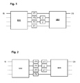
- Fig. 1 shows a modulator, in which two multimode interferometers MMI are linked together.
- the input signal IS is splitted in the first MMI into four branches, which have a defined phase shift to the input signal.
- the branches are grouped into pairs, which are modulated with opposite driving signals.
- the inphase portion I is modulated with the phase modulators +P1 and -P1, while the quadrature portion Q is modulated with the phase modulators +P2 and -P2.
- the fixed phase shifters P ⁇ compensate for the fixed phase shift of the branches.
- the dashed lines on the input and output of the MMIs indicate, that also 4X4 MMIs can be used. In this case on the first MMI only one input is used and on the second MMI only one output.
- Another option is to use 1:4 power splitters, in which the input/output waveguide is located in the center of the structure. This can be incorporated by adjusting the fixed phase shifts P accordingly.
- Fig. 2 another arrangement of the phase modulators between the two MMIs is shown.
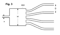
- Fig 3 depicts the structure of a MMI that splits the input signal into four outputs. This structure is according to the article titled " Design and Fabrication of 1-by-4 MMI Power Splitter for Optical Communication" of Huilian et.al. published in: Communications, 1999. APCC/OECC '99, pages 1638 - 1641 vol.2 .
- the width a is then 2 ⁇ m and the width W 40 ⁇ m.
- the distance D is 250 ⁇ m.
- the whole MMI measures 1 X 2 mm.
Landscapes
- Physics & Mathematics (AREA)
- Electromagnetism (AREA)
- Engineering & Computer Science (AREA)
- Computer Networks & Wireless Communication (AREA)
- Signal Processing (AREA)
- Optics & Photonics (AREA)
- Optical Modulation, Optical Deflection, Nonlinear Optics, Optical Demodulation, Optical Logic Elements (AREA)
Abstract
Description
- The invention relates to a modulator for the quadrature modulation of an optical carrier signal with an I- and a Q-portion.
- An optical I-Q-modulator is used in optical networks to transmit the data on the optical carrier signal in multilevel formats to achieve a high transmission data rate. The Q-portion of the carrier signal is shifted in relation to the I-portion by a fourth of the wavelength.
- The current method to implement an I-Q-modulator is to use separate Mach-Zehnder-interferometers for the I-portion and the Q-portion of the carrier signal. To split the signal, the Mach-Zehnder-interferometers are arranged in a Mach-Zehnder-Super-Structure. This involves a considerable number of components which are quite large in size and difficult to integrate.
- In the patent
US 7,063,601 an optical modulator is proposed in which a complex driver circuitry is used to build the driving signals for one Mach-Zehnder-modulator. This also leads to a complex structure. - It is the object of the invention to propose an I-Q-modulator, which is easy to integrate and in this way to build one compact optical component.
- This objective is achieved with the features of claim 1.
- Favourable embodiments of the invention are disclosed in the dependent claims.
- A basic building element for such a modulator is a 4-port multimode interferometer, acting as a 1:4 power splitter, which splits the optical carrier signal into four branches. It is an optical integrated circuit with a low loss and good power balance at each branch, compactness and ease of fabrication.
- So the optical carrier signal is split into four branches, which carry intermediate signals of equal power.
- The four branches are grouped into two pairs and some branches contain fixed phase shifts in order to obtain pair-wise Mach-Zehnder-structures with a mutual phase shift of a quarter wavelength. In each pair of the intermediate signals the according portion of the carrier signal is modulated with a driving signal. To avoid frequency chirp, the modulation in each branch of the pair is in opposite polarity, in the so-called push-pull configuration. So the I-portion and the Q-portion of the carrier signal are modulated separately.
- The modulated signals are combined again in a second multimode interferometer into one quadrature-modulated optical output signal.
- This combination of multimode-interferometers, phase modulators and phase shifters can be integrated to a compact integrated optical circuit.
- In one embodiment the modulation is done with phase shifters using the electro-optical effect, where an applied driving voltage shifts the phase of the optical signal.
- In a further embodiment the modulation is done with amplitude modulators using the electro-absorption effect, where an applied driving voltage attenuates the amplitude of the optical signal. In this case, the integrated fixed phase shifts are such that each branch corresponds to one axis (+I, -I, +Q, - Q) of the I-Q constellation diagram.
- It is also possible to use waveguides as phase shifters which can be modulated.
- When building the optical circuit, the branches of the multimode interferometer can be formed as waveguides and the connecting branches of the first and the second multimode interferometer are used as straight waveguides, which can be modulated.
- In the figures some aspects of the modulator are shown.
- Fig. 1
- shows an embodiment with two pairs of branches, where one pair is phase shifted.
- Fig. 2
- shows another arrangement with three phase shift- ers.
- Fig. 3
- shows an implementation of an MMI.
-
Fig. 1 shows a modulator, in which two multimode interferometers MMI are linked together. The input signal IS is splitted in the first MMI into four branches, which have a defined phase shift to the input signal. The branches are grouped into pairs, which are modulated with opposite driving signals. The inphase portion I is modulated with the phase modulators +P1 and -P1, while the quadrature portion Q is modulated with the phase modulators +P2 and -P2. The fixed phase shifters P = π compensate for the fixed phase shift of the branches. - The dashed lines on the input and output of the MMIs indicate, that also 4X4 MMIs can be used. In this case on the first MMI only one input is used and on the second MMI only one output. Another option is to use 1:4 power splitters, in which the input/output waveguide is located in the center of the structure. This can be incorporated by adjusting the fixed phase shifts P accordingly.
- In
Fig. 2 another arrangement of the phase modulators between the two MMIs is shown. In the two pairs for the I-Portion P1 and the Q-portion P2 always a phase shift of P/2 = π/2 is achieved. -
Fig 3 depicts the structure of a MMI that splits the input signal into four outputs. This structure is according to the article titled "Design and Fabrication of 1-by-4 MMI Power Splitter for Optical Communication" of Huilian et.al. published in: Communications, 1999. APCC/OECC '99, pages 1638 - 1641 vol.2. - It is an all optical component, where the input signal is fed into the input structure with the width a, then the structure is widened to the width W and fed into the four branches, which bend to a cento-to-center distance D between neighboring branches. In these branches modulating waveguides can be implemented.
- The component, described in said article, is designed for the wavelength of the optical signal λ = 1,31 µm. The width a is then 2 µm and the width W 40 µm. The distance D is 250 µm. The whole MMI measures 1
X 2 mm. - This shows that a very compact I-Q-modulator for optical signals can be built, which is all in optical technology.
-
- a
- Width of input stucture
- D
- Distence of branches
- IS
- Input Signal
- MMI
- Multi Mode Interferometer
- OS
- Output Signal
- W
- Width of MMI
- P1
- Phase shifter of the I-portion
- P2
- Phase shifter of the Q-portion
- p, p/2
- Fixed phase shifters
Claims (8)
- Modulator for the quadrature modulation of an optical carrier signal with an I- and a Q-portion,
characterized in that
a first optical multimode interferometer (MMI) splits the optical carrier signal into four branches and that in pairs of branches the I-portion and the Q-portion respectively is modulated with a Mach-Zehnder-Structure and
a second optical multimode interferometer (MMI) combines the modulated I-portion and Q-portion again to one quadrature modulated optical output signal (OS). - A modulator according to claim 1, characterized in that the Mach-Zehnder-Structure is built by optical phase shifters (p, p/2) which are inserted into two or more branches.
- A modulator according to claim 1, characterized in that the modulation is executed with a bias, which compensates for phase differences or nonlinearities.
- A modulator according to claim 1, characterized in that the modulation is an amplitude modulation.
- A modulator according to claim 1, characterized in that the modulation is a phase modulation.
- A modulator according to claim 5, characterized in that the phase modulation is achieved by the electro- absorption effect.
- A modulator according to claim 4, characterized in that the amplitude modulation is achieved by the electro-optic effect.
- A modulator according to claim 1, characterized in that the branches of the first and the second multimode interferometer (MMI), which connect the two, are built as as waveguides which can be modulated.
Priority Applications (3)
| Application Number | Priority Date | Filing Date | Title |
|---|---|---|---|
| EP08104643.5A EP2141833B1 (en) | 2008-07-04 | 2008-07-04 | Optical I-Q-modulator |
| US13/002,551 US8295710B2 (en) | 2008-07-04 | 2009-07-06 | Optical I-Q-modulator |
| PCT/EP2009/058472 WO2010000863A1 (en) | 2008-07-04 | 2009-07-06 | Optical i-q-modulator |
Applications Claiming Priority (1)
| Application Number | Priority Date | Filing Date | Title |
|---|---|---|---|
| EP08104643.5A EP2141833B1 (en) | 2008-07-04 | 2008-07-04 | Optical I-Q-modulator |
Publications (2)
| Publication Number | Publication Date |
|---|---|
| EP2141833A1 true EP2141833A1 (en) | 2010-01-06 |
| EP2141833B1 EP2141833B1 (en) | 2013-10-16 |
Family
ID=40020234
Family Applications (1)
| Application Number | Title | Priority Date | Filing Date |
|---|---|---|---|
| EP08104643.5A Not-in-force EP2141833B1 (en) | 2008-07-04 | 2008-07-04 | Optical I-Q-modulator |
Country Status (3)
| Country | Link |
|---|---|
| US (1) | US8295710B2 (en) |
| EP (1) | EP2141833B1 (en) |
| WO (1) | WO2010000863A1 (en) |
Cited By (2)
| Publication number | Priority date | Publication date | Assignee | Title |
|---|---|---|---|---|
| EP2908449A1 (en) * | 2014-02-18 | 2015-08-19 | Alcatel Lucent | Device for transmitting and/or modulating optical signals with passive phase shifters |
| CN105388564A (en) * | 2015-12-03 | 2016-03-09 | 中国科学院半导体研究所 | InP-base few-mode photo integrated emission chip based on MMI coupler |
Families Citing this family (62)
| Publication number | Priority date | Publication date | Assignee | Title |
|---|---|---|---|---|
| GB0718706D0 (en) | 2007-09-25 | 2007-11-07 | Creative Physics Ltd | Method and apparatus for reducing laser speckle |
| US9335604B2 (en) | 2013-12-11 | 2016-05-10 | Milan Momcilo Popovich | Holographic waveguide display |
| US11726332B2 (en) | 2009-04-27 | 2023-08-15 | Digilens Inc. | Diffractive projection apparatus |
| US11320571B2 (en) | 2012-11-16 | 2022-05-03 | Rockwell Collins, Inc. | Transparent waveguide display providing upper and lower fields of view with uniform light extraction |
| US10795160B1 (en) | 2014-09-25 | 2020-10-06 | Rockwell Collins, Inc. | Systems for and methods of using fold gratings for dual axis expansion |
| US8233204B1 (en) | 2009-09-30 | 2012-07-31 | Rockwell Collins, Inc. | Optical displays |
| US11300795B1 (en) | 2009-09-30 | 2022-04-12 | Digilens Inc. | Systems for and methods of using fold gratings coordinated with output couplers for dual axis expansion |
| US8659826B1 (en) | 2010-02-04 | 2014-02-25 | Rockwell Collins, Inc. | Worn display system and method without requiring real time tracking for boresight precision |
| US9274349B2 (en) | 2011-04-07 | 2016-03-01 | Digilens Inc. | Laser despeckler based on angular diversity |
| US10670876B2 (en) | 2011-08-24 | 2020-06-02 | Digilens Inc. | Waveguide laser illuminator incorporating a despeckler |
| WO2016020630A2 (en) | 2014-08-08 | 2016-02-11 | Milan Momcilo Popovich | Waveguide laser illuminator incorporating a despeckler |
| EP2995986B1 (en) | 2011-08-24 | 2017-04-12 | Rockwell Collins, Inc. | Data display |
| US8634139B1 (en) | 2011-09-30 | 2014-01-21 | Rockwell Collins, Inc. | System for and method of catadioptric collimation in a compact head up display (HUD) |
| US9599813B1 (en) | 2011-09-30 | 2017-03-21 | Rockwell Collins, Inc. | Waveguide combiner system and method with less susceptibility to glare |
| US9366864B1 (en) | 2011-09-30 | 2016-06-14 | Rockwell Collins, Inc. | System for and method of displaying information without need for a combiner alignment detector |
| US9715067B1 (en) | 2011-09-30 | 2017-07-25 | Rockwell Collins, Inc. | Ultra-compact HUD utilizing waveguide pupil expander with surface relief gratings in high refractive index materials |
| WO2013102759A2 (en) | 2012-01-06 | 2013-07-11 | Milan Momcilo Popovich | Contact image sensor using switchable bragg gratings |
| US9523852B1 (en) | 2012-03-28 | 2016-12-20 | Rockwell Collins, Inc. | Micro collimator system and method for a head up display (HUD) |
| WO2013163347A1 (en) | 2012-04-25 | 2013-10-31 | Rockwell Collins, Inc. | Holographic wide angle display |
| US9933684B2 (en) | 2012-11-16 | 2018-04-03 | Rockwell Collins, Inc. | Transparent waveguide display providing upper and lower fields of view having a specific light output aperture configuration |
| US9674413B1 (en) | 2013-04-17 | 2017-06-06 | Rockwell Collins, Inc. | Vision system and method having improved performance and solar mitigation |
| US9727772B2 (en) | 2013-07-31 | 2017-08-08 | Digilens, Inc. | Method and apparatus for contact image sensing |
| US9244281B1 (en) | 2013-09-26 | 2016-01-26 | Rockwell Collins, Inc. | Display system and method using a detached combiner |
| US10732407B1 (en) | 2014-01-10 | 2020-08-04 | Rockwell Collins, Inc. | Near eye head up display system and method with fixed combiner |
| US9519089B1 (en) | 2014-01-30 | 2016-12-13 | Rockwell Collins, Inc. | High performance volume phase gratings |
| US9977310B2 (en) | 2014-03-10 | 2018-05-22 | Alcatel Lucent | Multi-electrode photonic digital to analog converting vector modulator |
| US9244280B1 (en) | 2014-03-25 | 2016-01-26 | Rockwell Collins, Inc. | Near eye display system and method for display enhancement or redundancy |
| US10359736B2 (en) | 2014-08-08 | 2019-07-23 | Digilens Inc. | Method for holographic mastering and replication |
| US10241330B2 (en) | 2014-09-19 | 2019-03-26 | Digilens, Inc. | Method and apparatus for generating input images for holographic waveguide displays |
| US9715110B1 (en) | 2014-09-25 | 2017-07-25 | Rockwell Collins, Inc. | Automotive head up display (HUD) |
| US10088675B1 (en) | 2015-05-18 | 2018-10-02 | Rockwell Collins, Inc. | Turning light pipe for a pupil expansion system and method |
| EP3245444B1 (en) | 2015-01-12 | 2021-09-08 | DigiLens Inc. | Environmentally isolated waveguide display |
| US9632226B2 (en) | 2015-02-12 | 2017-04-25 | Digilens Inc. | Waveguide grating device |
| US10126552B2 (en) | 2015-05-18 | 2018-11-13 | Rockwell Collins, Inc. | Micro collimator system and method for a head up display (HUD) |
| US11366316B2 (en) | 2015-05-18 | 2022-06-21 | Rockwell Collins, Inc. | Head up display (HUD) using a light pipe |
| US10247943B1 (en) | 2015-05-18 | 2019-04-02 | Rockwell Collins, Inc. | Head up display (HUD) using a light pipe |
| US9618821B2 (en) | 2015-06-05 | 2017-04-11 | Lumentum Operations Llc | Optical modulator |
| US10108010B2 (en) | 2015-06-29 | 2018-10-23 | Rockwell Collins, Inc. | System for and method of integrating head up displays and head down displays |
| CN113759555B (en) | 2015-10-05 | 2024-09-20 | 迪吉伦斯公司 | Waveguide Display |
| US10598932B1 (en) | 2016-01-06 | 2020-03-24 | Rockwell Collins, Inc. | Head up display for integrating views of conformally mapped symbols and a fixed image source |
| WO2017162999A1 (en) | 2016-03-24 | 2017-09-28 | Popovich Milan Momcilo | Method and apparatus for providing a polarization selective holographic waveguide device |
| US10890707B2 (en) | 2016-04-11 | 2021-01-12 | Digilens Inc. | Holographic waveguide apparatus for structured light projection |
| EP3548939A4 (en) | 2016-12-02 | 2020-11-25 | DigiLens Inc. | WAVE GUIDE DEVICE WITH UNIFORM OUTPUT LIGHTING |
| WO2018129398A1 (en) | 2017-01-05 | 2018-07-12 | Digilens, Inc. | Wearable heads up displays |
| US10295824B2 (en) | 2017-01-26 | 2019-05-21 | Rockwell Collins, Inc. | Head up display with an angled light pipe |
| US10942430B2 (en) | 2017-10-16 | 2021-03-09 | Digilens Inc. | Systems and methods for multiplying the image resolution of a pixelated display |
| US10914950B2 (en) | 2018-01-08 | 2021-02-09 | Digilens Inc. | Waveguide architectures and related methods of manufacturing |
| US10732569B2 (en) | 2018-01-08 | 2020-08-04 | Digilens Inc. | Systems and methods for high-throughput recording of holographic gratings in waveguide cells |
| KR20250004154A (en) | 2018-01-08 | 2025-01-07 | 디지렌즈 인코포레이티드. | Methods for fabricating optical waveguides |
| US20190212588A1 (en) | 2018-01-08 | 2019-07-11 | Digilens, Inc. | Systems and Methods for Manufacturing Waveguide Cells |
| WO2020023779A1 (en) | 2018-07-25 | 2020-01-30 | Digilens Inc. | Systems and methods for fabricating a multilayer optical structure |
| WO2020149956A1 (en) | 2019-01-14 | 2020-07-23 | Digilens Inc. | Holographic waveguide display with light control layer |
| US20200247017A1 (en) | 2019-02-05 | 2020-08-06 | Digilens Inc. | Methods for Compensating for Optical Surface Nonuniformity |
| CN113692544B (en) | 2019-02-15 | 2025-04-22 | 迪吉伦斯公司 | Method and apparatus for providing holographic waveguide displays using integrated gratings |
| US20220283377A1 (en) | 2019-02-15 | 2022-09-08 | Digilens Inc. | Wide Angle Waveguide Display |
| US20200292745A1 (en) | 2019-03-12 | 2020-09-17 | Digilens Inc. | Holographic Waveguide Backlight and Related Methods of Manufacturing |
| CN114207492A (en) | 2019-06-07 | 2022-03-18 | 迪吉伦斯公司 | Waveguide with transmission grating and reflection grating and method for producing the same |
| US11681143B2 (en) | 2019-07-29 | 2023-06-20 | Digilens Inc. | Methods and apparatus for multiplying the image resolution and field-of-view of a pixelated display |
| KR102775783B1 (en) | 2019-08-29 | 2025-02-28 | 디지렌즈 인코포레이티드. | Vacuum grid and method for manufacturing the same |
| WO2022150841A1 (en) | 2021-01-07 | 2022-07-14 | Digilens Inc. | Grating structures for color waveguides |
| EP4288831A4 (en) | 2021-03-05 | 2025-01-15 | Digilens Inc. | EVACUATED PERIODIC STRUCTURES AND THEIR MANUFACTURING PROCESSES |
| CN115276804A (en) * | 2021-04-30 | 2022-11-01 | 华为技术有限公司 | Optical power adjusting system and optical power adjusting device |
Citations (5)
| Publication number | Priority date | Publication date | Assignee | Title |
|---|---|---|---|---|
| US5109441A (en) * | 1991-01-18 | 1992-04-28 | General Instrument Corporation | Fiber optic external modulator |
| WO1998053367A1 (en) * | 1997-05-21 | 1998-11-26 | Kestrel Solutions, Inc. | Electro-optic modulator with improved harmonic performance |
| US20060034616A1 (en) * | 2004-08-13 | 2006-02-16 | Alan Tipper | Automatic bias control for an optical modulator |
| US7063601B1 (en) | 2005-01-19 | 2006-06-20 | Sejong University Industry-Academy Cooperation Foundation | Internal magnetic-force polishing system |
| US20060210283A1 (en) * | 2004-09-20 | 2006-09-21 | Arasor Corporation | Transmitters for inversely dispersed optical signals |
Family Cites Families (3)
| Publication number | Priority date | Publication date | Assignee | Title |
|---|---|---|---|---|
| US5483369A (en) * | 1993-11-03 | 1996-01-09 | At&T Corp. | Communication systems using passive RF routing |
| AU2002311612A1 (en) * | 2001-06-18 | 2003-01-02 | Orchid Lightwave Communications, Inc. | Electro-optic waveguide modulator method and apparatus |
| US7636501B2 (en) * | 2007-12-31 | 2009-12-22 | Alcatel-Lucent Usa Inc. | QAM optical modulators |
-
2008
- 2008-07-04 EP EP08104643.5A patent/EP2141833B1/en not_active Not-in-force
-
2009
- 2009-07-06 US US13/002,551 patent/US8295710B2/en active Active
- 2009-07-06 WO PCT/EP2009/058472 patent/WO2010000863A1/en not_active Ceased
Patent Citations (5)
| Publication number | Priority date | Publication date | Assignee | Title |
|---|---|---|---|---|
| US5109441A (en) * | 1991-01-18 | 1992-04-28 | General Instrument Corporation | Fiber optic external modulator |
| WO1998053367A1 (en) * | 1997-05-21 | 1998-11-26 | Kestrel Solutions, Inc. | Electro-optic modulator with improved harmonic performance |
| US20060034616A1 (en) * | 2004-08-13 | 2006-02-16 | Alan Tipper | Automatic bias control for an optical modulator |
| US20060210283A1 (en) * | 2004-09-20 | 2006-09-21 | Arasor Corporation | Transmitters for inversely dispersed optical signals |
| US7063601B1 (en) | 2005-01-19 | 2006-06-20 | Sejong University Industry-Academy Cooperation Foundation | Internal magnetic-force polishing system |
Non-Patent Citations (3)
| Title |
|---|
| HITOSHI MURAI ET AL: "EA-Modulator-Based Optical Time Division Multiplexing/Demultiplexing Techniques for 160-Gb/s Optical Signal Transmission", IEEE JOURNAL OF SELECTED TOPICS IN QUANTUM ELECTRONICS, IEEE SERVICE CENTER, PISCATAWAY, NJ, US, vol. 13, no. 1, 1 January 2007 (2007-01-01), pages 70 - 78, XP011163499, ISSN: 1077-260X * |
| HITOSHI MURAI: "EA-Modulator based Optical Time division Multiplexing/Demultiplexing Techniques for 160-Gb/s Optical Signal Transmission", IEEE JOURNAL OF SELECTED TOPICS IN QUANTUM ELECTRONICS, vol. 13, 1 January 2007 (2007-01-01), pages 70 - 78, XP011163499 |
| HUILIAN: "Design and Fabrication of 1-by-4 MMI Power Splitter for Optical Communication", COMMUNICATIONS, 1999. APCC/OECC '99, vol. 2, pages 1638 - 1641 |
Cited By (4)
| Publication number | Priority date | Publication date | Assignee | Title |
|---|---|---|---|---|
| EP2908449A1 (en) * | 2014-02-18 | 2015-08-19 | Alcatel Lucent | Device for transmitting and/or modulating optical signals with passive phase shifters |
| US9547214B2 (en) | 2014-02-18 | 2017-01-17 | Commissariat à l'Energie Atomique et aux Energies Alternatives (“CEA”) | Device for transmitting and/or modulating optical signals with passive phase shifters |
| CN105388564A (en) * | 2015-12-03 | 2016-03-09 | 中国科学院半导体研究所 | InP-base few-mode photo integrated emission chip based on MMI coupler |
| CN105388564B (en) * | 2015-12-03 | 2018-03-23 | 中国科学院半导体研究所 | The few mould integreted phontonics transmitting chip of InP-base based on MMI couplers |
Also Published As
| Publication number | Publication date |
|---|---|
| EP2141833B1 (en) | 2013-10-16 |
| US20110164305A1 (en) | 2011-07-07 |
| US8295710B2 (en) | 2012-10-23 |
| WO2010000863A1 (en) | 2010-01-07 |
Similar Documents
| Publication | Publication Date | Title |
|---|---|---|
| US8295710B2 (en) | Optical I-Q-modulator | |
| EP2453295B1 (en) | Optical modulator | |
| US9618821B2 (en) | Optical modulator | |
| JP5215857B2 (en) | Light modulator | |
| US8295712B2 (en) | Optical device and method for optical frequency modulation to optical amplitude modulation conversion | |
| US9485032B2 (en) | Optical multilevel transmitter and optical transponder | |
| EP2409430B1 (en) | Optical single-sideband transmitter | |
| US7941011B2 (en) | Multilevel light intensity modulator | |
| JP4934557B2 (en) | 4-level phase modulator | |
| US20140153075A1 (en) | Optical signal modulation | |
| CN103370892B (en) | Optical frequency shifter and optical modulator using the optical frequency shifter | |
| US20060159466A1 (en) | Offset quadrature phase-shift-keying method and optical transmitter using the same | |
| US8238758B2 (en) | Three-arm DQPSK modulator | |
| US6535316B1 (en) | Generation of high-speed digital optical signals | |
| JP2013122546A (en) | Semiconductor optical phase modulator and method for driving the same | |
| Hasan et al. | Integrated optical SSB modulation/frequency shifting using cascaded silicon MZM | |
| US20020080454A1 (en) | Method, system and apparatus for optically transferring information | |
| WO2022009324A1 (en) | Optical transmitter | |
| JP7541270B2 (en) | Optical modulation circuit and digital signal processing method | |
| EP2659602B1 (en) | An optical duobinary modulated signal generator | |
| US8023776B2 (en) | Mach-Zehnder type optical modulator | |
| JP6106062B2 (en) | Light modulator | |
| Ringel et al. | Low-Vπ, coupling-optimized, single-ended push-pull ring-assisted Mach-Zehnder modulators for integration with high-speed, low-swing voltage drivers in integrated silicon-photonic platforms | |
| CN117728896A (en) | An optical time division multiplexing device, method, transmitter and transmission system | |
| Cincotti | New planar architectures for optical digital modulators |
Legal Events
| Date | Code | Title | Description |
|---|---|---|---|
| PUAI | Public reference made under article 153(3) epc to a published international application that has entered the european phase |
Free format text: ORIGINAL CODE: 0009012 |
|
| AK | Designated contracting states |
Kind code of ref document: A1 Designated state(s): AT BE BG CH CY CZ DE DK EE ES FI FR GB GR HR HU IE IS IT LI LT LU LV MC MT NL NO PL PT RO SE SI SK TR |
|
| AX | Request for extension of the european patent |
Extension state: AL BA MK RS |
|
| 17P | Request for examination filed |
Effective date: 20100706 |
|
| 17Q | First examination report despatched |
Effective date: 20100803 |
|
| AKX | Designation fees paid |
Designated state(s): AT BE BG CH CY CZ DE DK EE ES FI FR GB GR HR HU IE IS IT LI LT LU LV MC MT NL NO PL PT RO SE SI SK TR |
|
| REG | Reference to a national code |
Ref country code: DE Ref legal event code: R079 Ref document number: 602008028081 Country of ref document: DE Free format text: PREVIOUS MAIN CLASS: H04B0010155000 Ipc: H04B0010516000 |
|
| RIC1 | Information provided on ipc code assigned before grant |
Ipc: H04B 10/516 20130101AFI20130312BHEP |
|
| GRAP | Despatch of communication of intention to grant a patent |
Free format text: ORIGINAL CODE: EPIDOSNIGR1 |
|
| INTG | Intention to grant announced |
Effective date: 20130529 |
|
| GRAS | Grant fee paid |
Free format text: ORIGINAL CODE: EPIDOSNIGR3 |
|
| GRAA | (expected) grant |
Free format text: ORIGINAL CODE: 0009210 |
|
| AK | Designated contracting states |
Kind code of ref document: B1 Designated state(s): AT BE BG CH CY CZ DE DK EE ES FI FR GB GR HR HU IE IS IT LI LT LU LV MC MT NL NO PL PT RO SE SI SK TR |
|
| REG | Reference to a national code |
Ref country code: GB Ref legal event code: FG4D |
|
| REG | Reference to a national code |
Ref country code: CH Ref legal event code: EP |
|
| REG | Reference to a national code |
Ref country code: IE Ref legal event code: FG4D |
|
| RAP2 | Party data changed (patent owner data changed or rights of a patent transferred) |
Owner name: NOKIA SOLUTIONS AND NETWORKS OY |
|
| REG | Reference to a national code |
Ref country code: AT Ref legal event code: REF Ref document number: 636928 Country of ref document: AT Kind code of ref document: T Effective date: 20131115 |
|
| RAP2 | Party data changed (patent owner data changed or rights of a patent transferred) |
Owner name: XIEON NETWORKS S.A.R.L. |
|
| REG | Reference to a national code |
Ref country code: DE Ref legal event code: R096 Ref document number: 602008028081 Country of ref document: DE Effective date: 20131212 |
|
| REG | Reference to a national code |
Ref country code: GB Ref legal event code: 732E Free format text: REGISTERED BETWEEN 20140130 AND 20140205 |
|
| REG | Reference to a national code |
Ref country code: NL Ref legal event code: VDEP Effective date: 20131016 |
|
| REG | Reference to a national code |
Ref country code: AT Ref legal event code: MK05 Ref document number: 636928 Country of ref document: AT Kind code of ref document: T Effective date: 20131016 |
|
| REG | Reference to a national code |
Ref country code: LT Ref legal event code: MG4D |
|
| PG25 | Lapsed in a contracting state [announced via postgrant information from national office to epo] |
Ref country code: LT Free format text: LAPSE BECAUSE OF FAILURE TO SUBMIT A TRANSLATION OF THE DESCRIPTION OR TO PAY THE FEE WITHIN THE PRESCRIBED TIME-LIMIT Effective date: 20131016 Ref country code: FI Free format text: LAPSE BECAUSE OF FAILURE TO SUBMIT A TRANSLATION OF THE DESCRIPTION OR TO PAY THE FEE WITHIN THE PRESCRIBED TIME-LIMIT Effective date: 20131016 Ref country code: HR Free format text: LAPSE BECAUSE OF FAILURE TO SUBMIT A TRANSLATION OF THE DESCRIPTION OR TO PAY THE FEE WITHIN THE PRESCRIBED TIME-LIMIT Effective date: 20131016 Ref country code: BE Free format text: LAPSE BECAUSE OF FAILURE TO SUBMIT A TRANSLATION OF THE DESCRIPTION OR TO PAY THE FEE WITHIN THE PRESCRIBED TIME-LIMIT Effective date: 20131016 Ref country code: IS Free format text: LAPSE BECAUSE OF FAILURE TO SUBMIT A TRANSLATION OF THE DESCRIPTION OR TO PAY THE FEE WITHIN THE PRESCRIBED TIME-LIMIT Effective date: 20140216 Ref country code: NO Free format text: LAPSE BECAUSE OF FAILURE TO SUBMIT A TRANSLATION OF THE DESCRIPTION OR TO PAY THE FEE WITHIN THE PRESCRIBED TIME-LIMIT Effective date: 20140116 Ref country code: NL Free format text: LAPSE BECAUSE OF FAILURE TO SUBMIT A TRANSLATION OF THE DESCRIPTION OR TO PAY THE FEE WITHIN THE PRESCRIBED TIME-LIMIT Effective date: 20131016 Ref country code: SE Free format text: LAPSE BECAUSE OF FAILURE TO SUBMIT A TRANSLATION OF THE DESCRIPTION OR TO PAY THE FEE WITHIN THE PRESCRIBED TIME-LIMIT Effective date: 20131016 |
|
| REG | Reference to a national code |
Ref country code: FR Ref legal event code: GC Effective date: 20140408 |
|
| PG25 | Lapsed in a contracting state [announced via postgrant information from national office to epo] |
Ref country code: AT Free format text: LAPSE BECAUSE OF FAILURE TO SUBMIT A TRANSLATION OF THE DESCRIPTION OR TO PAY THE FEE WITHIN THE PRESCRIBED TIME-LIMIT Effective date: 20131016 Ref country code: CY Free format text: LAPSE BECAUSE OF FAILURE TO SUBMIT A TRANSLATION OF THE DESCRIPTION OR TO PAY THE FEE WITHIN THE PRESCRIBED TIME-LIMIT Effective date: 20131016 Ref country code: LV Free format text: LAPSE BECAUSE OF FAILURE TO SUBMIT A TRANSLATION OF THE DESCRIPTION OR TO PAY THE FEE WITHIN THE PRESCRIBED TIME-LIMIT Effective date: 20131016 Ref country code: ES Free format text: LAPSE BECAUSE OF FAILURE TO SUBMIT A TRANSLATION OF THE DESCRIPTION OR TO PAY THE FEE WITHIN THE PRESCRIBED TIME-LIMIT Effective date: 20131016 |
|
| PG25 | Lapsed in a contracting state [announced via postgrant information from national office to epo] |
Ref country code: PT Free format text: LAPSE BECAUSE OF FAILURE TO SUBMIT A TRANSLATION OF THE DESCRIPTION OR TO PAY THE FEE WITHIN THE PRESCRIBED TIME-LIMIT Effective date: 20140217 |
|
| REG | Reference to a national code |
Ref country code: DE Ref legal event code: R097 Ref document number: 602008028081 Country of ref document: DE |
|
| PG25 | Lapsed in a contracting state [announced via postgrant information from national office to epo] |
Ref country code: EE Free format text: LAPSE BECAUSE OF FAILURE TO SUBMIT A TRANSLATION OF THE DESCRIPTION OR TO PAY THE FEE WITHIN THE PRESCRIBED TIME-LIMIT Effective date: 20131016 |
|
| PLBE | No opposition filed within time limit |
Free format text: ORIGINAL CODE: 0009261 |
|
| STAA | Information on the status of an ep patent application or granted ep patent |
Free format text: STATUS: NO OPPOSITION FILED WITHIN TIME LIMIT |
|
| PG25 | Lapsed in a contracting state [announced via postgrant information from national office to epo] |
Ref country code: RO Free format text: LAPSE BECAUSE OF FAILURE TO SUBMIT A TRANSLATION OF THE DESCRIPTION OR TO PAY THE FEE WITHIN THE PRESCRIBED TIME-LIMIT Effective date: 20131016 Ref country code: PL Free format text: LAPSE BECAUSE OF FAILURE TO SUBMIT A TRANSLATION OF THE DESCRIPTION OR TO PAY THE FEE WITHIN THE PRESCRIBED TIME-LIMIT Effective date: 20131016 Ref country code: CZ Free format text: LAPSE BECAUSE OF FAILURE TO SUBMIT A TRANSLATION OF THE DESCRIPTION OR TO PAY THE FEE WITHIN THE PRESCRIBED TIME-LIMIT Effective date: 20131016 Ref country code: IT Free format text: LAPSE BECAUSE OF FAILURE TO SUBMIT A TRANSLATION OF THE DESCRIPTION OR TO PAY THE FEE WITHIN THE PRESCRIBED TIME-LIMIT Effective date: 20131016 Ref country code: SK Free format text: LAPSE BECAUSE OF FAILURE TO SUBMIT A TRANSLATION OF THE DESCRIPTION OR TO PAY THE FEE WITHIN THE PRESCRIBED TIME-LIMIT Effective date: 20131016 |
|
| 26N | No opposition filed |
Effective date: 20140717 |
|
| PG25 | Lapsed in a contracting state [announced via postgrant information from national office to epo] |
Ref country code: DK Free format text: LAPSE BECAUSE OF FAILURE TO SUBMIT A TRANSLATION OF THE DESCRIPTION OR TO PAY THE FEE WITHIN THE PRESCRIBED TIME-LIMIT Effective date: 20131016 |
|
| REG | Reference to a national code |
Ref country code: DE Ref legal event code: R097 Ref document number: 602008028081 Country of ref document: DE Effective date: 20140717 |
|
| PG25 | Lapsed in a contracting state [announced via postgrant information from national office to epo] |
Ref country code: SI Free format text: LAPSE BECAUSE OF FAILURE TO SUBMIT A TRANSLATION OF THE DESCRIPTION OR TO PAY THE FEE WITHIN THE PRESCRIBED TIME-LIMIT Effective date: 20131016 Ref country code: LU Free format text: LAPSE BECAUSE OF FAILURE TO SUBMIT A TRANSLATION OF THE DESCRIPTION OR TO PAY THE FEE WITHIN THE PRESCRIBED TIME-LIMIT Effective date: 20140704 |
|
| REG | Reference to a national code |
Ref country code: CH Ref legal event code: PL |
|
| REG | Reference to a national code |
Ref country code: IE Ref legal event code: MM4A |
|
| PG25 | Lapsed in a contracting state [announced via postgrant information from national office to epo] |
Ref country code: LI Free format text: LAPSE BECAUSE OF NON-PAYMENT OF DUE FEES Effective date: 20140731 Ref country code: CH Free format text: LAPSE BECAUSE OF NON-PAYMENT OF DUE FEES Effective date: 20140731 |
|
| REG | Reference to a national code |
Ref country code: FR Ref legal event code: PLFP Year of fee payment: 8 |
|
| PG25 | Lapsed in a contracting state [announced via postgrant information from national office to epo] |
Ref country code: IE Free format text: LAPSE BECAUSE OF NON-PAYMENT OF DUE FEES Effective date: 20140704 |
|
| REG | Reference to a national code |
Ref country code: FR Ref legal event code: GC Effective date: 20150922 |
|
| PG25 | Lapsed in a contracting state [announced via postgrant information from national office to epo] |
Ref country code: MC Free format text: LAPSE BECAUSE OF FAILURE TO SUBMIT A TRANSLATION OF THE DESCRIPTION OR TO PAY THE FEE WITHIN THE PRESCRIBED TIME-LIMIT Effective date: 20131016 |
|
| PG25 | Lapsed in a contracting state [announced via postgrant information from national office to epo] |
Ref country code: BG Free format text: LAPSE BECAUSE OF FAILURE TO SUBMIT A TRANSLATION OF THE DESCRIPTION OR TO PAY THE FEE WITHIN THE PRESCRIBED TIME-LIMIT Effective date: 20131016 |
|
| PG25 | Lapsed in a contracting state [announced via postgrant information from national office to epo] |
Ref country code: GR Free format text: LAPSE BECAUSE OF FAILURE TO SUBMIT A TRANSLATION OF THE DESCRIPTION OR TO PAY THE FEE WITHIN THE PRESCRIBED TIME-LIMIT Effective date: 20140117 Ref country code: MT Free format text: LAPSE BECAUSE OF FAILURE TO SUBMIT A TRANSLATION OF THE DESCRIPTION OR TO PAY THE FEE WITHIN THE PRESCRIBED TIME-LIMIT Effective date: 20131016 |
|
| REG | Reference to a national code |
Ref country code: FR Ref legal event code: PLFP Year of fee payment: 9 |
|
| PG25 | Lapsed in a contracting state [announced via postgrant information from national office to epo] |
Ref country code: HU Free format text: LAPSE BECAUSE OF FAILURE TO SUBMIT A TRANSLATION OF THE DESCRIPTION OR TO PAY THE FEE WITHIN THE PRESCRIBED TIME-LIMIT; INVALID AB INITIO Effective date: 20080704 Ref country code: TR Free format text: LAPSE BECAUSE OF FAILURE TO SUBMIT A TRANSLATION OF THE DESCRIPTION OR TO PAY THE FEE WITHIN THE PRESCRIBED TIME-LIMIT Effective date: 20131016 |
|
| REG | Reference to a national code |
Ref country code: FR Ref legal event code: PLFP Year of fee payment: 10 |
|
| REG | Reference to a national code |
Ref country code: FR Ref legal event code: PLFP Year of fee payment: 11 |
|
| PGFP | Annual fee paid to national office [announced via postgrant information from national office to epo] |
Ref country code: FR Payment date: 20180725 Year of fee payment: 11 Ref country code: DE Payment date: 20180723 Year of fee payment: 11 |
|
| PGFP | Annual fee paid to national office [announced via postgrant information from national office to epo] |
Ref country code: GB Payment date: 20180719 Year of fee payment: 11 |
|
| REG | Reference to a national code |
Ref country code: DE Ref legal event code: R119 Ref document number: 602008028081 Country of ref document: DE |
|
| GBPC | Gb: european patent ceased through non-payment of renewal fee |
Effective date: 20190704 |
|
| PG25 | Lapsed in a contracting state [announced via postgrant information from national office to epo] |
Ref country code: GB Free format text: LAPSE BECAUSE OF NON-PAYMENT OF DUE FEES Effective date: 20190704 Ref country code: DE Free format text: LAPSE BECAUSE OF NON-PAYMENT OF DUE FEES Effective date: 20200201 |
|
| PG25 | Lapsed in a contracting state [announced via postgrant information from national office to epo] |
Ref country code: FR Free format text: LAPSE BECAUSE OF NON-PAYMENT OF DUE FEES Effective date: 20190731 |