EP2141533A1 - Contrast compensation of microdisplay panels including a high order waveplate - Google Patents
Contrast compensation of microdisplay panels including a high order waveplate Download PDFInfo
- Publication number
- EP2141533A1 EP2141533A1 EP09164273A EP09164273A EP2141533A1 EP 2141533 A1 EP2141533 A1 EP 2141533A1 EP 09164273 A EP09164273 A EP 09164273A EP 09164273 A EP09164273 A EP 09164273A EP 2141533 A1 EP2141533 A1 EP 2141533A1
- Authority
- EP
- European Patent Office
- Prior art keywords
- order
- plate
- liquid crystal
- waveplate
- retardance
- Prior art date
- Legal status (The legal status is an assumption and is not a legal conclusion. Google has not performed a legal analysis and makes no representation as to the accuracy of the status listed.)
- Granted
Links
- 239000004973 liquid crystal related substance Substances 0.000 claims abstract description 117
- 239000000758 substrate Substances 0.000 claims abstract description 91
- 239000010409 thin film Substances 0.000 claims abstract description 14
- 229910052594 sapphire Inorganic materials 0.000 claims description 118
- 239000010980 sapphire Substances 0.000 claims description 118
- 239000010453 quartz Substances 0.000 claims description 69
- VYPSYNLAJGMNEJ-UHFFFAOYSA-N silicon dioxide Inorganic materials O=[Si]=O VYPSYNLAJGMNEJ-UHFFFAOYSA-N 0.000 claims description 69
- 239000010410 layer Substances 0.000 claims description 43
- 239000006185 dispersion Substances 0.000 claims description 18
- 230000003595 spectral effect Effects 0.000 claims description 14
- 230000005540 biological transmission Effects 0.000 claims description 12
- 239000002356 single layer Substances 0.000 claims description 5
- 230000003287 optical effect Effects 0.000 description 14
- 239000004065 semiconductor Substances 0.000 description 11
- 230000010287 polarization Effects 0.000 description 10
- 239000000463 material Substances 0.000 description 9
- 239000013078 crystal Substances 0.000 description 8
- 230000000694 effects Effects 0.000 description 8
- 238000010586 diagram Methods 0.000 description 7
- 238000004519 manufacturing process Methods 0.000 description 7
- 239000010408 film Substances 0.000 description 6
- 238000001228 spectrum Methods 0.000 description 5
- XUIMIQQOPSSXEZ-UHFFFAOYSA-N Silicon Chemical compound [Si] XUIMIQQOPSSXEZ-UHFFFAOYSA-N 0.000 description 4
- 239000011521 glass Substances 0.000 description 4
- 238000005286 illumination Methods 0.000 description 4
- 229910052710 silicon Inorganic materials 0.000 description 4
- 239000010703 silicon Substances 0.000 description 4
- 238000009501 film coating Methods 0.000 description 3
- 239000011159 matrix material Substances 0.000 description 3
- 230000008033 biological extinction Effects 0.000 description 2
- 238000000576 coating method Methods 0.000 description 2
- 238000013461 design Methods 0.000 description 2
- 230000006872 improvement Effects 0.000 description 2
- 101001132548 Mus musculus Ras-related protein Rab-9A Proteins 0.000 description 1
- 235000010724 Wisteria floribunda Nutrition 0.000 description 1
- -1 amorphous Chemical compound 0.000 description 1
- 238000004873 anchoring Methods 0.000 description 1
- 238000013459 approach Methods 0.000 description 1
- 230000015556 catabolic process Effects 0.000 description 1
- 229920002678 cellulose Polymers 0.000 description 1
- 239000001913 cellulose Substances 0.000 description 1
- 230000008859 change Effects 0.000 description 1
- 230000000295 complement effect Effects 0.000 description 1
- 238000006731 degradation reaction Methods 0.000 description 1
- 230000001419 dependent effect Effects 0.000 description 1
- 238000000151 deposition Methods 0.000 description 1
- 230000005686 electrostatic field Effects 0.000 description 1
- 238000005516 engineering process Methods 0.000 description 1
- 230000001747 exhibiting effect Effects 0.000 description 1
- 239000011888 foil Substances 0.000 description 1
- 230000017525 heat dissipation Effects 0.000 description 1
- AMGQUBHHOARCQH-UHFFFAOYSA-N indium;oxotin Chemical compound [In].[Sn]=O AMGQUBHHOARCQH-UHFFFAOYSA-N 0.000 description 1
- 230000028161 membrane depolarization Effects 0.000 description 1
- 238000000034 method Methods 0.000 description 1
- 230000037230 mobility Effects 0.000 description 1
- 238000012986 modification Methods 0.000 description 1
- 230000004048 modification Effects 0.000 description 1
- 229910021421 monocrystalline silicon Inorganic materials 0.000 description 1
- 239000002985 plastic film Substances 0.000 description 1
- 229920006255 plastic film Polymers 0.000 description 1
- 229910021420 polycrystalline silicon Inorganic materials 0.000 description 1
- 229920000642 polymer Polymers 0.000 description 1
- 229920005591 polysilicon Polymers 0.000 description 1
- 230000035945 sensitivity Effects 0.000 description 1
- 238000013519 translation Methods 0.000 description 1
- 239000012780 transparent material Substances 0.000 description 1
- ILJSQTXMGCGYMG-UHFFFAOYSA-N triacetic acid Chemical compound CC(=O)CC(=O)CC(O)=O ILJSQTXMGCGYMG-UHFFFAOYSA-N 0.000 description 1
Images












Classifications
-
- G—PHYSICS
- G02—OPTICS
- G02F—OPTICAL DEVICES OR ARRANGEMENTS FOR THE CONTROL OF LIGHT BY MODIFICATION OF THE OPTICAL PROPERTIES OF THE MEDIA OF THE ELEMENTS INVOLVED THEREIN; NON-LINEAR OPTICS; FREQUENCY-CHANGING OF LIGHT; OPTICAL LOGIC ELEMENTS; OPTICAL ANALOGUE/DIGITAL CONVERTERS
- G02F1/00—Devices or arrangements for the control of the intensity, colour, phase, polarisation or direction of light arriving from an independent light source, e.g. switching, gating or modulating; Non-linear optics
- G02F1/01—Devices or arrangements for the control of the intensity, colour, phase, polarisation or direction of light arriving from an independent light source, e.g. switching, gating or modulating; Non-linear optics for the control of the intensity, phase, polarisation or colour
- G02F1/13—Devices or arrangements for the control of the intensity, colour, phase, polarisation or direction of light arriving from an independent light source, e.g. switching, gating or modulating; Non-linear optics for the control of the intensity, phase, polarisation or colour based on liquid crystals, e.g. single liquid crystal display cells
- G02F1/133—Constructional arrangements; Operation of liquid crystal cells; Circuit arrangements
- G02F1/1333—Constructional arrangements; Manufacturing methods
- G02F1/1335—Structural association of cells with optical devices, e.g. polarisers or reflectors
- G02F1/13363—Birefringent elements, e.g. for optical compensation
- G02F1/133632—Birefringent elements, e.g. for optical compensation with refractive index ellipsoid inclined relative to the LC-layer surface
-
- G—PHYSICS
- G02—OPTICS
- G02F—OPTICAL DEVICES OR ARRANGEMENTS FOR THE CONTROL OF LIGHT BY MODIFICATION OF THE OPTICAL PROPERTIES OF THE MEDIA OF THE ELEMENTS INVOLVED THEREIN; NON-LINEAR OPTICS; FREQUENCY-CHANGING OF LIGHT; OPTICAL LOGIC ELEMENTS; OPTICAL ANALOGUE/DIGITAL CONVERTERS
- G02F1/00—Devices or arrangements for the control of the intensity, colour, phase, polarisation or direction of light arriving from an independent light source, e.g. switching, gating or modulating; Non-linear optics
- G02F1/01—Devices or arrangements for the control of the intensity, colour, phase, polarisation or direction of light arriving from an independent light source, e.g. switching, gating or modulating; Non-linear optics for the control of the intensity, phase, polarisation or colour
- G02F1/13—Devices or arrangements for the control of the intensity, colour, phase, polarisation or direction of light arriving from an independent light source, e.g. switching, gating or modulating; Non-linear optics for the control of the intensity, phase, polarisation or colour based on liquid crystals, e.g. single liquid crystal display cells
- G02F1/133—Constructional arrangements; Operation of liquid crystal cells; Circuit arrangements
- G02F1/1333—Constructional arrangements; Manufacturing methods
- G02F1/1335—Structural association of cells with optical devices, e.g. polarisers or reflectors
- G02F1/13363—Birefringent elements, e.g. for optical compensation
- G02F1/133638—Waveplates, i.e. plates with a retardation value of lambda/n
-
- G—PHYSICS
- G02—OPTICS
- G02F—OPTICAL DEVICES OR ARRANGEMENTS FOR THE CONTROL OF LIGHT BY MODIFICATION OF THE OPTICAL PROPERTIES OF THE MEDIA OF THE ELEMENTS INVOLVED THEREIN; NON-LINEAR OPTICS; FREQUENCY-CHANGING OF LIGHT; OPTICAL LOGIC ELEMENTS; OPTICAL ANALOGUE/DIGITAL CONVERTERS
- G02F1/00—Devices or arrangements for the control of the intensity, colour, phase, polarisation or direction of light arriving from an independent light source, e.g. switching, gating or modulating; Non-linear optics
- G02F1/01—Devices or arrangements for the control of the intensity, colour, phase, polarisation or direction of light arriving from an independent light source, e.g. switching, gating or modulating; Non-linear optics for the control of the intensity, phase, polarisation or colour
- G02F1/13—Devices or arrangements for the control of the intensity, colour, phase, polarisation or direction of light arriving from an independent light source, e.g. switching, gating or modulating; Non-linear optics for the control of the intensity, phase, polarisation or colour based on liquid crystals, e.g. single liquid crystal display cells
- G02F1/133—Constructional arrangements; Operation of liquid crystal cells; Circuit arrangements
- G02F1/136—Liquid crystal cells structurally associated with a semi-conducting layer or substrate, e.g. cells forming part of an integrated circuit
- G02F1/1362—Active matrix addressed cells
- G02F1/136277—Active matrix addressed cells formed on a semiconductor substrate, e.g. of silicon
Definitions
- the present application relates generally to contrast compensation, and in particular, to contrast compensation of liquid crystal microdisplay panels including a high order waveplate.
- LC microdisplays are widely found in projections systems, as for example used in business presentations and home entertainment (e.g., large screen televisions). In general, these relatively small displays (e.g., typically measuring less than 1.5" diagonally) are coupled with one or more optical lenses that enlarge the projected image to a suitable display size.
- LC microdisplays have been based on one of two types of technologies, namely a reflective-type microdisplay (e.g., liquid crystal on silicon (LCoS)) or a transmissive-type microdisplay.
- a reflective-type microdisplay e.g., liquid crystal on silicon (LCoS)
- transmissive-type microdisplay e.g., liquid crystal on silicon
- a typical transmissive LC microdisplay includes a layer of liquid crystal material (e.g., vertical-aligned (VA)-mode, in-plane switching (IPS)-mode, planar aligned (PA)-mode, or, more commonly, 90 degree twisted nematic (TN)-mode) sandwiched between front and back transparent plates.
- the back plate includes a patterned electrode layer, while the front plate includes a common electrode layer, each of which is typically formed from a transparent material such as indium tin oxide (ITO).
- ITO indium tin oxide
- the front and back plates typically include alignment layers that are aligned perpendicular to each other such that the LC molecules are arranged in a helical structure or twist.
- the twisted arrangement rotates the polarization of incident linearly polarized light by about 180 degrees.
- the LC molecules In the presence of a sufficiently large applied voltage (i.e., on-state), the LC molecules begin to untwist such that the polarization of the linearly polarized incident light is not rotated.
- This LC cell is typically disposed between a polarizer and analyzer having parallel transmission axes (i.e., normally-black) or, more commonly, perpendicular transmission axes (i.e., normally-white).
- transmissive LC microdisplays typically use an active matrix system, wherein a matrix of thin-film transistors (TFTs) controls the voltage applied by the electrodes. More specifically, each TFT functions as a switching element that controls the orientation of LC in each display pixel.
- the active TFT layer has been formed by depositing silicon (e.g., amorphous, poly, or crystalline) on a glass back plate. More recently, the advantages of using sapphire as the substrate for the silicon layer have been realized. For example, sapphire exhibits optical transparency in the visible band and is a semiconductor that promotes the growth of single crystal silicon, thus reducing manufacturing complexity and costs.
- sapphire is desirable for TFT fabrication because it has high electron and hole mobilities, which enables high speed logic switching. Furthermore, it has higher thermal conductivity than the conventional glass substrates used in high-temperature polysilicon TFTs, thus providing efficient heat dissipation in high brightness illumination systems.
- the internal polarizer is stated to significantly improve the contrast of a transparent microdisplay built on sapphire substrate, the improvement is achieved at the expense of lost light intensity (e.g., the internal polarizer filters out a portion of the light transmitted through the sapphire substrate having elliptical polarization).
- the instant invention relates to a contrast compensator, which, for example, can be used to improve the panel contrast of liquid crystal (LC) microdisplays having a sapphire plate.
- the contrast compensator includes a high order waveplate, which has a thickness and symmetry selected to compensate for variations in spectral and angular linear retardance, across the useful wavelength band (e.g., visible) and angle range (e.g., ⁇ 12 degrees of cone illumination) found in transparent semiconductor substrates used for LC TFT (e.g., sapphire).
- a liquid crystal microdisplay comprising: a liquid crystal microdisplay panel including a first substrate, a second substrate, and a liquid crystal layer disposed between the first and second substrates, the first substrate including a first multiple-order waveplate configured as an O-plate and supporting a thin film transistor layer; and, a retarder compensator for compensating for spectral and angular linear retardance dispersions of the first substrate, the retarder compensator including a second multiple-order waveplate configured as an O-plate, the second multiple-order waveplate having a birefringence opposite in sign to a birefringence of the first multiple-order waveplate.
- FIG. 1A is a cross-section of a transmissive LC panel
- FIG. 1B illustrates the configuration of the high-order sapphire substrate shown in FIG. 1A ;
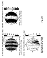
- FIG. 2A shows a linear retardance map for an experimental TN-mode LC panel having a high-order sapphire substrate
- FIG. 2B shows a linear retardance map for a numerical TN-mode LC panel having a high-order sapphire substrate
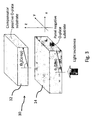
- FIG. 3 is a schematic diagram of a retarder compensator in accordance with one embodiment of the instant invention in tandem with a high-order sapphire substrate;
- FIG. 4 shows the spectral and angular linear retardance curve fitting results of a quartz retarder compensator and a high-order sapphire substrate
- FIG. 5 shows a qualitative comparison of the linear retardance maps calculated for the quartz retarder compensator and the high-order sapphire substrate using modeled retardance data for both the quartz retarder compensator and the high order sapphire substrate;
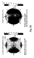
- FIG. 6A shows the net retardance and conoscopic leakage calculated for the quartz compensator cascaded with the high-order sapphire substrate in the blue band using modeled retardance data for both the quartz retarder compensator and the high order sapphire substrate;
- FIG. 6B shows the net retardance and conoscopic leakage calculated for the quartz compensator cascaded with the high-order sapphire substrate in the green band using modeled retardance data for both the quartz retarder compensator and the high order sapphire substrate;
- FIG. 6C shows the net retardance and conoscopic leakage calculated for the quartz compensator cascaded with the high-order sapphire substrate in the red band using modeled retardance data for both the quartz retarder compensator and the high order sapphire substrate;
- FIG. 7 shows a qualitative comparison of the linear retardance maps for the quartz retarder compensator and the high-order sapphire substrate using experimental retardance data for the high order sapphire substrate;
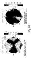
- FIG. 8A shows the net retardance and conoscopic leakage for the quartz compensator cascaded with the high-order sapphire substrate in the blue band using experimental retardance data for the high order sapphire substrate;
- FIG. 8B shows the net retardance and conoscopic leakage for the quartz compensator cascaded with the high-order sapphire substrate in the green band using experimental retardance data for the high order sapphire substrate;
- FIG. 8C shows the net retardance and conoscopic leakage for the quartz compensator cascaded with the high-order sapphire substrate in the red band using experimental retardance data for the high order sapphire substrate;
- FIG. 9 shows plots of calculated contrast ratio for a range of quartz layer thickness, C-axis polar angles, and C-axis azimuthal angles
- FIG. 10 shows plots of azimuthal angle, polar angle, and thickness tolerances for the cascaded arrangement
- FIG. 11 is a schematic diagram illustrating beam walk-off in thick birefringent crystal plates
- FIG. 12 shows plots of walk-off versus C-axis tilt for high-order sapphire and quartz plates
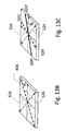
- FIG. 13A is a schematic diagram illustrating the sixteen possible combinations of sapphire C-axis and TN LC slow axis orientations
- FIG. 13B is a schematic diagram illustrating the slow axis orientation of the trim retarder when the retardances are matched
- FIG. 13C is a schematic diagram illustrating possible slow axis orientations of the trim retarder when the retardances are mismatched
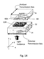
- FIG. 14 is a schematic diagram of a retarder compensator in accordance with one embodiment of the instant invention in tandem with a trim retarder, the TN-mode LC layer, and the high-order sapphire substrate;
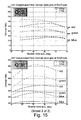
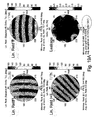
- FIG. 15 shows plots of contrast ratio versus retarder slow axis for the possible slow axis orientations of the trim retarder, when the trim retarder is a single layer A-plate;
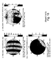
- FIG. 16 shows a qualitative comparison of the linear retardance maps calculated for the A-plate on quartz compensator and the TN/sapphire panel using modeled retardance data
- FIG. 17 shows the net retardance and conoscopic leakage calculated for the A-plate on quartz compensator and the TN/sapphire panel in the blue, green, and red bands using modeled retardance data
- FIG. 18 shows the net retardance and conoscopic leakage calculated for the A-plate on quartz compensator and the TN/sapphire panel in the blue, green, and red bands using experimental retardance data for the TN/sapphire panel;
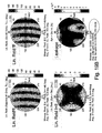
- FIG. 19 shows a comparison of the linear retardance maps and conoscopic leakage maps for two sapphire plates in a cross-axes configuration and for sapphire/quartz plates in a parallel configuration
- FIG. 20 shows a schematic diagram of a 3-panel transmissive LC microdisplay projection system light engine.
- Panel contrast ratio which refers generally to the ratio of the light intensity in the bright state to the light intensity of in the dark state, is an important characteristic of LC microdisplays.
- the panel contrast ratio is significantly reduced when the panel is viewed obliquely.
- the variation in contrast ratio due to viewing angle is typically referred to as the viewing angle characteristic.
- a retarder compensator is often used.
- the retarder compensator is typically placed between the polarizer and the LC cell and/or between the analyzer and the LC cell.
- the retarder compensator will include multiple layers of birefringent materials each having different physical thicknesses, optical axis orientation with respect to the liquid crystal and polarizer angles, or sign of birefringence.
- contrast enhancement retarder compensators in order to provide for efficient contrast enhancement retarder compensators often include one or more A-plates (e.g., a uniaxial birefringent element having its optic axis parallel to the surface of the element), C-plates (e.g., a uniaxial birefringent element having its optic axis normal to the surface of the element), and/or O-plates (e.g., a uniaxial birefringent element having its optic axis at an oblique angle to the surface of the element), each of which may be positive or negative.
- A-plates e.g., a uniaxial birefringent element having its optic axis parallel to the surface of the element
- C-plates e.g., a uniaxial birefringent element having its optic axis normal to the surface of the element
- O-plates e.g., a uniaxial birefringent element having its optic axis at an oblique angle
- a retarder compensator used in a VA-mode LC microdisplay may include a tilted O-plate having in-plane retardance and out-of-plane retardance, the latter of which is used for field-of-view (FOV) enhancement, while a retarder compensator used in a TN-mode LC microdisplay may exhibit in-plane retardance, out-of-plane retardance, and circular retardance.
- FOV field-of-view
- the retarder compensator is used to compensate for a relatively low-magnitude retardance (e.g., often less than about 50 nm in-plane retardance), which for example, is exhibited by the LC layer in the dark state.
- retarder compensators are often referred to as trim retarder compensators, or simply trim retarders.
- trim retarders were fabricated as compensating films.
- trim retarders have been fabricated out of stretched organic foil, such as Fuji's Wide View (WV) film TM , which consists of a discotic layer on a triacetate cellulose (TAC) substrate.
- WV Fuji's Wide View
- TAC triacetate cellulose
- Providing the trim retardance with a compensating film and/or thin film coating allows the trim retarder to be fabricated as a true zero-order waveplate.
- a zero-order waveplate provides only the required phase delay (i.e., a phase delay of only 0.25 waves is provided if the retarder is a zero-order quarter-wave plate).
- a multiple-order waveplate provides a relative phase delay that is larger than the required phase delay by some characteristic value (e.g., an integer multiple of 2 ⁇ larger for a full waveplate or an odd integer multiple of ⁇ /2 larger for a quarter waveplate).
- some characteristic value e.g., an integer multiple of 2 ⁇ larger for a full waveplate or an odd integer multiple of ⁇ /2 larger for a quarter waveplate.
- a multiple-order wave retarder should behave similarly to a zero-order wave retarder.
- a tenth-order quarter-wave plate (e.g., 5.25 waves) should behave similarly to a zero-order quarter-wave plate (e.g., 0.25 waves), for a given wavelength.
- multiple-order waveplates have not been typically used as trim retarders due to their high dispersion and temperature dependence.
- the high dispersion which results in not all wavelength channels within the visible band being compensated adequately, is particularly problematic in transmissive LCD projectors, which usually include more than LC microdisplay (e.g., one for each of the blue 460 nm, green 550 nm, and red 620 nm, bands).
- a sapphire semiconductor substrate is a birefringent crystal plate that is transparent in the visible band. Even though the birefringence of a sapphire plate is relative low (e.g., approximately 0.008 at 550nm), the thickness required to provide sufficient support in LC cell sandwiching (e.g., a physical thickness between 0.4mm to 1mm), will yield several microns of retardance.
- sapphire semiconductor substrates are often configured as O-plates.
- the R-plane is a crystal cut that yields the optic axis or C-axis alignment of the sapphire at about 57.6 degrees with respect to plate normal.
- This O-plate configuration means there is a large retardance slope as a function of angle of incidence at viewing planes close to the C-axis tilt plane.
- the high order retardances gives rise to alternating even and odd retardance order where the effective retardance at normal incidence varies from 0 to ⁇ several times within the visible band.
- These retardance variations degrade the achievable panel contrast, and in particular degrade the viewing angle characteristics. For example, degradation will occur through a cross-polarizer setup when the corresponding linear retarder axis is not aligned parallel/perpendicular to the polarizers.
- the transmissive LC panel 10 includes a LC layer 12 sandwiched between the sapphire back plate 14 and a cover plate 16.
- the LC layer 12 is formed from a LC material such as 90 degree twisted nematic (TN)-mode, vertical-aligned (VA)-mode, in-plane switching (IPS)-mode, or planar aligned (PA)-mode LC.
- the sapphire back plate 14 is a birefringent crystal plate, which supports an active matrix pixel addressing circuit (not shown) used to control the orientation of the LC director in the LC layer 12.
- the cover plate 16 is a glass plate.
- the transmissive LC panel 10 will also include one or more electrodes 18A, 18B and one or more alignment layers 19A, 19B.
- the transmissive LC panel 10 will be disposed between two polarizers 20A, 20B.
- the two polarizers 20A, 20B are oriented such that their transmission axes are perpendicular, then the first polarizer 20A is typically referred to as the polarizer while the second polarizer 20B is referred to as the analyzer. Referring to FIG.
- the C-axis of the sapphire substrate 14 is oriented at a polar angle of 57.6 degrees (i.e., its C-axis tilt is at 57.6 degrees from the substrate normal), while the R-plane is coincident with the surface of the plate.
- the C-axis of the sapphire back plate 14 is typically aligned parallel or perpendicular to the transmission axis of the polarizer 20A.
- FIGS. 2A and 2B Experimental and calculated FOV retardance data for a LC panel 10 similar to that shown in FIG. 1A is shown in FIGS. 2A and 2B , respectively.
- the LC layer included TN-mode LC exhibiting about 10 nm in-plane retardance in the dark state, while the sapphire back plate was about 600 microns thick.
- the ordinary index, n o , and the extraordinary index, n e , of sapphire were assumed to be 1.7706 and 1.7650, respectively, giving a birefringence, ⁇ n , equal to -0.0081 at 550 nm. Full dispersion over the visible band was utilized.
- the thickness of the sapphire back plate was 576.6 microns.
- the sapphire back plate is a 12 th order waveplate.
- the sapphire back plate is a high-order negative O-plate.
- the net retardance is 45 degrees in the 12 th order at 530 nm (2205 degrees unwrapped).
- the retardance wrapped to the 0 th order changes rapidly with polar/azimuthal angles of incidence.
- the average linear retardance at normal incidence was 44.1 degrees.
- the average linear retardance at normal incidence was 47.4 degrees.
- a retarder compensator including a counter birefringent substrate which is also a high-order waveplate, is used to reduce the wavelength and angle dispersions of retardance introduced by the sapphire substrate, and thus improve the contrast ratio and viewing angle characteristics of the transmissive TN-mode LC microdisplay including the sapphire back plate.
- the counter birefringent plate 32 which is formed from a material having an opposite sign of birefringence relative to the sapphire substrate 14 (i.e., sapphire exhibits a negative birefringence so the birefringent plate 32 will have a positive birefringence), also has an oblique C-axis alignment versus the substrate normal (i.e., the birefringent plate 32 is a positive O-plate).
- the birefringent plate 32 is fabricated such that its C-axis orientation and its retardation order substantially complement the spectral and angular linear retardance profiles of the sapphire substrate 14.
- the two substrates function in tandem to significantly reduce the net retardance at all wavelength and angle points (e.g., ideally to zero).
- a quartz crystal plate has a positive birefringence and has approximately the same birefringence dispersion as a sapphire crystal plate. Accordingly, with appropriate choices of C-axis alignment and quartz substrate thickness, the compensating plate 32 and the sapphire substrate 14 will function in co-operation to provide for approximately equal and opposite sign retardance at every ray angle and every wavelength of operation. As a result, the system contrast is not negatively affected by the large retardance of the sapphire substrate 14.
- n o the ordinary index
- n e the extraordinary index
- the ordinary index, n o , and the extraordinary index, n e were assumed to be 1.5461 and 1.5554, respectively, giving a birefringence, ⁇ n , equal to +0.0092 at 550 nm. In each case, full dispersion over the visible band was utilized.
- the spectral retardance dispersion (e.g., left-hand plot) and angular retardance dispersion (e.g., right-hand plot) of the quartz and sapphire plates can be simultaneously matched with suitable quartz parameters.
- suitable quartz parameters For example, numerical results indicate that if the quartz compensating plate has a C-axis tilt that is about 61.1 degrees from the substrate normal and a physical thickness of about 472.0 microns, then the spectral and/or angular retardance dispersions will be substantially matched.
- the quartz compensating plate is also a 12 th order waveplate.
- FIGS. 6A , 6B , 6C illustrate the calculated contrast in the blue (e.g., 458 nm), green (e.g., 522nm), and red (e.g., 624 nm) bands, respectively, when the C-axis azimuthal angle of the sapphire substrate is parallel to the C-axis azimuthal angle of the quartz compensating plate. More specifically, the left-hand plots show the net linear retardance of the sapphire substrate/quartz compensating plate combination (i.e., disregarding other retardation contributions such as from the LC layer and/or the corresponding trim retarder compensator), whereas the right-hand plots show the ideal crossed polarizer raw contrast (e.g., which is not weighted by the system baseline).
- the left-hand plots show the net linear retardance of the sapphire substrate/quartz compensating plate combination (i.e., disregarding other retardation contributions such as from the LC layer and/or the corresponding trim retarder compensator)
- the average normal incidence retardance is 2.8 degrees for the blue band, 3.2 degrees for the green band, and 5.9 degrees for the red band, indicating that the birefringence compensation is nearly complete.
- the calculated two-stage contrast ranges from about 17k in the blue band, 29k in the green band, and 28k in the red band.
- the modeled single-pass contrast of a two-stage system comprising of a sapphire panel substrate and a quartz compensating plate achieves greater than 20,000:1 in the green and red bands.
- the quartz compensating plate parameters were fitted to match experimental retardance data of a sapphire substrate 14.
- the experimental data was collected with the C-axis plane of the sapphire plate oriented parallel to the X-axis.
- the experimental spectrum data is shown with the dashed line.
- the spectral retardance dispersion (e.g., left-hand plot) and angular retardance dispersion (e.g., right-hand plot) calculated for quartz and experimentally obtained for sapphire can be also substantially matched.
- the contrast ratio in the blue (e.g., 458nm), green (e.g., 522nm), and red (e.g., 624nm) bands were calculated for a nominal quartz plate.
- the top graph shows the calculated contrast ratio for a quartz plate where the thickness is varied between 469.0 ⁇ 2 microns
- the middle graph shows the calculated contrast ratio for a quartz plate where the C-axis tilt or polar angle ⁇ c is varied between 61.0 ⁇ 0.5
- the bottom graph shows the contrast ratio calculated when the quartz plate is rotated within the plane of the plate by ⁇ 1 degree from the ideal alignment wherein the C-axis of the quartz plate and the sapphire plate are in the same tilt plane.
- the calculated contrast ratio results indicate that in order to maintain more than 50% of the peak contrast in the green band, the thickness tolerance of the quartz plate should be ⁇ 1 %, while the tilt axis tolerance should be ⁇ 0.5%.
- the calculated contrast ratios indicate that the quartz c-axis tilt plane should be within ⁇ 0.7 degrees of the sapphire tilt plane.
- the relationship between thickness, d, polar angle, ⁇ c , and azimuthal angle, ⁇ c , errors is shown.
- the azimuthal angle tolerances shown in the bottom two plots translate into typical Bell-shape contrast roll-off.
- the relationship between polar angle and substrate thickness errors illustrated in the top plot confirm that the tilt angle and thickness of the compensating quartz plate are dependent on each other in order to provide the required in-plane retardance, and thus improved contrast ratio.
- a larger tilt angle will generally be associated with a thinner plate to meet the in-plane retardance requirements, while a smaller tilt angle will yield a thicker plate.
- a quartz O-plate diced such that the C-axis is about 61 degrees versus the plate normal, provides substantially matched spectral and angular retardation variations to the sapphire substrate used in TFT fabrication, when the quartz plate is about 475 microns thick and the sapphire substrate is about 585 microns thick with a tilt angle of about 58 degrees.
- the C-axis plane of the quartz compensating plate is nominally aligned to the C-axis plane of the sapphire substrate.
- this two-stage parallel-aligned arrangement also provides image blur compensation.
- the substrate-mode extraordinary-wave walk-off from the o-wave direction is about 2.5 microns for a 585 micron thick substrate. Accordingly, depending on the position of the sapphire substrate 14 in the LC cell 10 relative to the incident light, this walk-off may produce two sets of images that are transmitted to the analyzer 20B. Any incomplete extinction of the analyzer of one set of images will result in crosstalk (e.g., image blur).
- FIG. 11 illustrates the walk-off through the relatively thick crystals plates (i.e., where the sapphire substrate 14 has a nominal thickness of 585 microns and the quartz compensating plate has a nominal thickness of 475 microns).
- FIG. 12 there is a larger deviation for the quartz plate than the sapphire substrate. However, since the quartz plate is thinner than the sapphire substrate the amount of lateral translation is almost equal for both plates.
- the two images are brought together again and the sensitivity to complete extinction of one set of images by the analyser is reduced.
- the blur compensation makes the contrast ratio less sensitive to whether the microdisplay is illuminated from the sapphire side or from the glass substrate side.
- the two-stage compensating system including the sapphire panel 14 and the quartz compensating plate 32 has been modeled and shown to provide an increased contrast ratio. More specifically, the high order quartz waveplate has been shown to remove the variations of spectra and angular linear retardance across the useful wavelength band (e.g., visible) and angle range (e.g., ⁇ 12 degrees of cone illumination) found in transparent semiconductor substrates such as sapphire, used for fabricating TFTs in transmissive LC microdisplays.
- the two-stage compensating system has been shown to provide improved contrast, the above-described calculations have not addressed the effects from the birefringent nature of the LC material in the LC microdisplay and/or a trim retarder.
- the slow axis of the TN layer 12 is typically aligned at a 45 degrees to the transmission axis of the polarizer 20A or analyzer 20B.
- the possible TN slow axis orientations when the transmission axes of the polarizer and analyser are parallel to the X and Y-axes, respectively, are represented by orientations Z, Q, P, and M.
- the C-axis of the sapphire back plate 14 is typically aligned parallel or perpendicular to the transmission axis of the analyzer 20B, yielding orientations N, E, S, and W.
- Table 1 Calculated Bare Panel Contrast TN LC Twist Angle Span and SA Angle SPH C-axis 45° (Z) 135° (Q) 225° (P) 315° (M) 0° (E) 121.4 85.3 97.0 91.0 90° (N) 102.0 97.1 106.9 129.9 180° (W) 122.8 91.4 104.6 89.6 270° (S) 115.9 120.8 82.7 97.0
- the numerical results indicate that the highest panel contrast over ⁇ 14 degree cone illumination is obtained when the C-axis of the sapphire plate is oriented at 90 degrees (i.e., orientation N) and when the TN panel slow axis substantially bisects the fourth quadrant (i.e., is oriented at -45 degrees, which corresponds to orientation M).
- orientation N the C-axis of the sapphire plate
- the calculated contrast ratio for the bare TN panel having its slow axis in the first, second, third and fourth quadrants of the panel are about 102, 97, 107, and 130:1, respectively.
- providing a LC panel having its slow axis in the fourth quadrant results in between 22% to 34% better contrast.
- the sapphire substrate 14 is configured as a high order negative O-plate having a 576.6 micron thickness and having a C-axis tilt 57.6 degrees from the surface normal.
- the LC-layer 12 is assumed to be part of a normally-white TN90 cell designed to provide for adiabatic waveguiding in the on-state (e.g., undriven) as extraordinary-waveguiding. In the absence of an applied voltage, the polarization of the incident light rotates with the twist angle of the LC molecules, which undergo a smooth 90 degree twist, such that the transmitted light is emitted with a polarization orthogonal to the polarization of the incident light.
- the electrostatic field generated by the applied voltage aligns the LC directors along the transmission axis of the cell (e.g., homeotropic alignment) such that the polarization of the incident light does not change upon passing through the LC cell.
- homeotropic alignment e.g., homeotropic alignment
- the entire cell is often described as having homeotropic alignment in the off-state, it is generally only the interior or mid-section of the LC cell that is truly homeotropic, since the LC directors close to the exit and entrance sections of the cell are influenced by the anchoring forces of the alignment layers.
- this intrinsic birefringence of the TN-mode LC layer in the dark state is assumed to correspond to about 10 nm of residual in-plane retardance in the green band (e.g., at 550 nm).
- the trim retarder 40 is often used to compensate for the residual in-plane retardance of the TN-mode LC in the dark state.
- the trim retarder 40 should have the same in-plane retardance exhibited by the TN90 panel in the dark state. Accordingly, when the slow axis 40A of the trim retarder is configured at orthogonal azimuthal orientation to the slow axis 12A of the LC panel then the net effect is zero relative delay for the incoming polarization.
- the trim retarder 40 it is more common to design the trim retarder 40 to have a higher in-plane retardance than the LC panel in order to accommodate for retardance variations due to manufacturing tolerances (e.g., in device thickness, etc.) and/or operational drifts (e.g., temperature, mechanical stress, etc.).
- manufacturing tolerances e.g., in device thickness, etc.
- operational drifts e.g., temperature, mechanical stress, etc.
- this mismatch in in-plane retardance requires offsetting of the slow axis 40A of the trim retarder relative to the nominal crossed axes configuration.
- the trim retarder is 'clocked-in' by rotating its azimuth orientation away from the crossed-axes configuration illustrated in FIG. 13B (e.g., where ⁇ r is equal to about 45 degrees) to one of four orientations (e.g., Q1P, Q1S, Q3P, Q3S).
- the sapphire substrate 14 is configured as a high order negative O-plate having a 576.6 micron thickness and having a C-axis tilt 57.6 degrees from the surface normal.
- the quartz compensating plate 32 is assumed to be configured as a high order positive O-plate having a thickness and C-axis tilt selected to substantially match the linear retardance spectral and angular variations of the sapphire substrate 14.
- the term high order is used to describe orders greater than 0, and more typically greater than about 2.
- each of the O-plate retarders 14, 32 is aligned parallel to the XZ plane (i.e., the C-axis of both the sapphire plate 14 and the quartz plate 32 are aligned with an azimuthal angle, ⁇ c , of about 0 degrees).
- the LC-layer 12 is assumed to be part of a normally-white TN90 cell designed to provide for adiabatic waveguiding in the on-state (e.g., undriven) as extraordinary-waveguiding.
- the alignment layers of the TN90 cell are arranged such that the LC molecules follow a counter clockwise (CCW) from the light input side to the light output side.
- CCW counter clockwise
- the slow axis 12A of the TN-mode LC layer is aligned such that it approximately bisects the 4 th quadrant of the TN90 panel.
- the intrinsic birefringence of the TN-mode LC layer in the dark state is assumed to correspond to about 10 nm of residual in-plane retardance in the green band (e.g., at 550 nm).
- the trim retarder 40 is assumed to be a single layer A-plate or O-plate that provides about 15 nm of in-plane retardance.
- the slow axis 40A of the trim retarder is clocked such that it is approximately 25 degrees CCW from the X-axis or 25 degrees clockwise (CW) from the Y-axis.
- the slow axis 40A of the trim retarder is aligned in one of the four orientations illustrated in FIG. 13C (i.e., Q1P, Q1S, Q3P, Q3S, where ⁇ r is equal to 25 degrees).
- FIG. 15 illustrates the calculated contrast ratios in the blue, green, and red bands and for both single layer A-plate and single layer O-plate configurations are shown for each of the four orientations (i.e., Q1P, Q1S, Q3P, Q3S). More specifically, FIG. 15 illustrates the calculated contrast ratios when the slow axis of the trim retarder is in the 1 st quadrant close to the P-axis (Q1P), is in the 1 st quadrant close to the S-axis (Q1S), in the 3 rd quadrant close to the P-axis (Q3P), and in the 3 rd quadrant close to the S-axis (Q3S).
- the calculated contrast ratios are higher for the A-plate than for the O-plate.
- the P-orientations i.e., Q3P and Q1P
- the A-plate solutions for the two solutions close to the S-axis i.e., Q1S and Q3S
- the two solutions close to the P-axis i.e., Q1P and Q3P
- the spectral retardance dispersion (e.g., left-hand plot) and angular retardance dispersion (e.g., right-hand plot) calculated for the A-plate trim retarder and the quartz plate can be substantially matched to that calculated for the TN-mode cell (i.e., modeled as the TN-layer and the sapphire panel).
- the angular retardance dispersion plot shows the retardance curve fitting along and orthogonal to the C-axis plane at the red, green, and blue band center wavelengths.
- FIG. 17 illustrates the calculated contrast in the blue (e.g., 460 nm), green (e.g., 550 nm), and red (e.g., 620 nm) bands, respectively, when the fitted parameters shown in FIG. 16 are used to model the sapphire panel 14 and TN-mode LC layer 12 compensated with the quartz plate 32 and A-plate 40.
- the contrast ratios are calculated to be about 340, 510 and 670:1, for the blue, green, and red wavelengths, respectively.
- the panel substrate FOV and TN LC layer in-plane retardance appear to be well compensated, there is some light leakage clustered around the 4 th quadrant. This light leakage is believed to arise from the lack of circular retardance compensation and the lack of TN-LC out-of-plane retardance compensation.
- the quartz/A-plate parameters were fitted to match the calculated wavelength and angle retardance spectra.
- the calculated contrast in the blue (e.g., 460 nm), green (e.g., 550 nm), and red (e.g., 620 nm) bands, respectively, is obtained when the quartz/A-plate parameters were fitted to match experimental wavelength and angle spectra.
- the actual panel FOV data gave a calculated 2-state contrast of about 180, 300, and 430:1 in the blue, green, and red bands, respectively.
- the largest leakage occurs in the fourth quadrant.
- a high order quartz compensating plate has been shown to significantly improve the contrast ratio of a TN-mode LC microdisplay having a sapphire substrate.
- tens of thousand to one contrast is achieved for sapphire plate/quartz plate combination.
- the calculated bare panel contrast e.g., 90:1 was improved to about 500:1 in the green band.
- a retarder compensator including a high-order O-plate retarder having a higher but oppositely signed birefringence than the high-order O-plate used as a back plate in a transmissive LC microdisplay has been found to provide improved contrast compensation over other compensation schemes.
- one approach to improving the contrast ratio of the projection display including sapphire substrate is to provide another sapphire plate having the same thickness and tilt angle, in a crossed-axes configuration. While this arrangement results in a Savart Plate, and thus should exhibit a net retardance of zero, the contrast ratio improvement has been found to not be as efficient as the high order waveplate aligned parallel to the sapphire plate.
- FIG. 19A shows the contour plots of the cross-axes sapphire/sapphire plates
- FIG. 19B shows contour plots of the parallel-axes sapphire/quart plates.
- the diagonal retardance bands of the cross-axes configuration reduces the off-axis contrast.
- the calculated contrast ratio for the cross-axes configuration was only 130:1, whereas the calculated contrast ratio for the parallel-axes configuration was 33,600:1.
- While a high-order quartz compensating plate has been shown to significantly improve contrast in a projections system utilizing a normally-white TN-mode LC microdisplay having a sapphire back plate (e.g., including pico-projectors), it is envisioned that the high-order compensating plate may be fabricated with other materials and/or may be used in projection systems based on other LC modes and/or incorporating a high-order retardance semiconductor substrate fabricated from a material other than sapphire. In addition, it is envisioned that the high-order compensating plate will be used with other retarder compensators (e.g., trim retarders) in order to further improve the system contrast.
- retarder compensators e.g., trim retarders
- the high-order retardance compensating plate 32 is coupled to the trim retarder 40.
- the trim retarder includes one or more birefringent or form-birefringent thin-film coatings deposited on the high-order retardance compensating plate, which are configured as A-plates, C-plates, and/or O-plates.
- the projector system advantageously achieves a high contrast with only one compensator assembly. Accordingly, only one compensator needs to be rotationally clocked, thus simplifying alignment.
- only two antireflection coatings are used (i.e., one on each of the external surfaces of the retarder compensator assembly).
- both the high-order retardance compensating plate 32 and the trim retarder 40 are used as stand-alone retarder elements.
- the high-order retardance compensating plate 32 is clocked to match the C-axis tilt plane of the high-order semiconductor substrate, while the trim retarder 40 is clocked to optimize compensation for the LC layer dark-state retardance.
- four anti-reflection coatings are used.
- the optical sub-system 100 includes input pre-polarizers 101a, 101b, 101c, retarder compensators 103a, 103b, 103c, TN-mode LC panels 104a, 104b, 104c, and exit clean-up polarizers 105a, 105b, 105c.
- the center element of the optical sub-system 100 is an X-cube 110, where three separate light beams 120a, 120b, 120c are aggregated and emitted as a converged light beam 130, which is projected onto a screen (not shown). The three separate light beams provide the RGB channel data.
- the green channel often corresponds to the first light beam 120a so that it is directed at the transmitted port of the X-cube.
- the LC panel 104a/104b/104c is positioned between a set of crossed polarizers (e.g., between an input pre-polarizer 101a/101b/101c and an exit clean-up polarizer 105a/105b/105c, respectively).
- the input pre-polarizers 101a, 101b, 101c have their transmission axes aligned horizontal (parallel to plane of drawing), while the exit clean-up polarizers 105a, 105b, 105c have their transmission axes aligned vertical.
- the arm of the optical sub-system 100 corresponding to the green or 'a' channel typically includes a half-waveplate (HWP) 106 to convert the modulated vertically polarized light to horizontally polarized light so that it appears as P-polarized light with respect to the X-cube hypotenuse and is transmitted through the X-cube.
- HWP half-waveplate
- the HWP 106 may be positioned in another arm of the optical sub-system 100.
- each of the retarder compensators 103a, 103b, 103c is shown to be disposed between the pre-polarizers 101a, 101b, 101c and the LC panels 104a/104b/104c, respectively, for exemplary purposes.
- the retarder compensators 103a, 103b, 103c are disposed between the LC panels 104a/104b/104c and the analyzers 105a, 105b, 105c, respectively.
- each the retarder compensator 103a, 103b, 103c includes a high order O-plate having a thickness and C-axis alignment selected to compensate for the in-plane and out-of-plane retardance of the transparent semiconductor substrate in the LC microdisplay used for TFT fabrication.
- In-plane retardance expressed as optical path length difference, refers to the difference between two orthogonal in-plane indices of refraction times the physical thickness of the optical element.
- Out-of-plane retardance refers to the difference of the index of refraction along the thickness direction (z direction) of the optical element and one in-plane index of refraction (or an average of in-plane indices of refraction), times the physical thickness of the optical element.
- the transparent semiconductor substrate which in one embodiment is a high-order retardance sapphire crystal plate, will be disposed on the light incident side of the LC panels 104a/104b/104c or the light exiting side of the LC panels 104a/104b/104c.
Landscapes
- Physics & Mathematics (AREA)
- Nonlinear Science (AREA)
- Optics & Photonics (AREA)
- Crystallography & Structural Chemistry (AREA)
- Chemical & Material Sciences (AREA)
- General Physics & Mathematics (AREA)
- Mathematical Physics (AREA)
- Polarising Elements (AREA)
- Liquid Crystal (AREA)
- Steroid Compounds (AREA)
- Vessels, Lead-In Wires, Accessory Apparatuses For Cathode-Ray Tubes (AREA)
- Liquid Crystal Substances (AREA)
- Gas-Filled Discharge Tubes (AREA)
- Transforming Electric Information Into Light Information (AREA)
Abstract
Description
- The present application relates generally to contrast compensation, and in particular, to contrast compensation of liquid crystal microdisplay panels including a high order waveplate.
- Liquid crystal (LC) microdisplays are widely found in projections systems, as for example used in business presentations and home entertainment (e.g., large screen televisions). In general, these relatively small displays (e.g., typically measuring less than 1.5" diagonally) are coupled with one or more optical lenses that enlarge the projected image to a suitable display size. Conventionally, LC microdisplays have been based on one of two types of technologies, namely a reflective-type microdisplay (e.g., liquid crystal on silicon (LCoS)) or a transmissive-type microdisplay.
- A typical transmissive LC microdisplay includes a layer of liquid crystal material (e.g., vertical-aligned (VA)-mode, in-plane switching (IPS)-mode, planar aligned (PA)-mode, or, more commonly, 90 degree twisted nematic (TN)-mode) sandwiched between front and back transparent plates. The back plate includes a patterned electrode layer, while the front plate includes a common electrode layer, each of which is typically formed from a transparent material such as indium tin oxide (ITO). When 90 degree TN-mode LC is used, the front and back plates typically include alignment layers that are aligned perpendicular to each other such that the LC molecules are arranged in a helical structure or twist. In the absence of an applied voltage (i.e., off-state), the twisted arrangement rotates the polarization of incident linearly polarized light by about 180 degrees. In the presence of a sufficiently large applied voltage (i.e., on-state), the LC molecules begin to untwist such that the polarization of the linearly polarized incident light is not rotated. This LC cell is typically disposed between a polarizer and analyzer having parallel transmission axes (i.e., normally-black) or, more commonly, perpendicular transmission axes (i.e., normally-white).
- In commercially available systems, transmissive LC microdisplays typically use an active matrix system, wherein a matrix of thin-film transistors (TFTs) controls the voltage applied by the electrodes. More specifically, each TFT functions as a switching element that controls the orientation of LC in each display pixel. Conventionally, the active TFT layer has been formed by depositing silicon (e.g., amorphous, poly, or crystalline) on a glass back plate. More recently, the advantages of using sapphire as the substrate for the silicon layer have been realized. For example, sapphire exhibits optical transparency in the visible band and is a semiconductor that promotes the growth of single crystal silicon, thus reducing manufacturing complexity and costs. In addition, sapphire is desirable for TFT fabrication because it has high electron and hole mobilities, which enables high speed logic switching. Furthermore, it has higher thermal conductivity than the conventional glass substrates used in high-temperature polysilicon TFTs, thus providing efficient heat dissipation in high brightness illumination systems.
- Unfortunately, the use of sapphire as a substrate for LC TFT fabrication has been found to have a negative effect on the panel contrast ratio of LC microdisplays. For example, in
US Pat. No. 7,480,017, Fisher et al. teach that the use of sapphire in LC microdisplays de-polarizes the light that passes through the liquid crystal material, reducing the on/off contrast ratio. Fisher et al. teach improving the contrast ratio by incorporating a wire grid or other polarizer on the active silicon back plate to correct for the depolarization of light passing through the sapphire substrate. While the internal polarizer is stated to significantly improve the contrast of a transparent microdisplay built on sapphire substrate, the improvement is achieved at the expense of lost light intensity (e.g., the internal polarizer filters out a portion of the light transmitted through the sapphire substrate having elliptical polarization). - The instant invention relates to a contrast compensator, which, for example, can be used to improve the panel contrast of liquid crystal (LC) microdisplays having a sapphire plate. The contrast compensator includes a high order waveplate, which has a thickness and symmetry selected to compensate for variations in spectral and angular linear retardance, across the useful wavelength band (e.g., visible) and angle range (e.g., ±12 degrees of cone illumination) found in transparent semiconductor substrates used for LC TFT (e.g., sapphire).
- In accordance with one aspect of the invention there is provided a liquid crystal microdisplay comprising: a liquid crystal microdisplay panel including a first substrate, a second substrate, and a liquid crystal layer disposed between the first and second substrates, the first substrate including a first multiple-order waveplate configured as an O-plate and supporting a thin film transistor layer; and, a retarder compensator for compensating for spectral and angular linear retardance dispersions of the first substrate, the retarder compensator including a second multiple-order waveplate configured as an O-plate, the second multiple-order waveplate having a birefringence opposite in sign to a birefringence of the first multiple-order waveplate.
- Further features and advantages of the present invention will become apparent from the following detailed description, taken in combination with the appended drawings, in which:
-
FIG. 1A is a cross-section of a transmissive LC panel; -
FIG. 1B illustrates the configuration of the high-order sapphire substrate shown inFIG. 1A ; -
FIG. 2A shows a linear retardance map for an experimental TN-mode LC panel having a high-order sapphire substrate; -
FIG. 2B shows a linear retardance map for a numerical TN-mode LC panel having a high-order sapphire substrate; -
FIG. 3 is a schematic diagram of a retarder compensator in accordance with one embodiment of the instant invention in tandem with a high-order sapphire substrate; -
FIG. 4 shows the spectral and angular linear retardance curve fitting results of a quartz retarder compensator and a high-order sapphire substrate; -
FIG. 5 shows a qualitative comparison of the linear retardance maps calculated for the quartz retarder compensator and the high-order sapphire substrate using modeled retardance data for both the quartz retarder compensator and the high order sapphire substrate; -
FIG. 6A shows the net retardance and conoscopic leakage calculated for the quartz compensator cascaded with the high-order sapphire substrate in the blue band using modeled retardance data for both the quartz retarder compensator and the high order sapphire substrate; -
FIG. 6B shows the net retardance and conoscopic leakage calculated for the quartz compensator cascaded with the high-order sapphire substrate in the green band using modeled retardance data for both the quartz retarder compensator and the high order sapphire substrate; -
FIG. 6C shows the net retardance and conoscopic leakage calculated for the quartz compensator cascaded with the high-order sapphire substrate in the red band using modeled retardance data for both the quartz retarder compensator and the high order sapphire substrate; -
FIG. 7 shows a qualitative comparison of the linear retardance maps for the quartz retarder compensator and the high-order sapphire substrate using experimental retardance data for the high order sapphire substrate; -
FIG. 8A shows the net retardance and conoscopic leakage for the quartz compensator cascaded with the high-order sapphire substrate in the blue band using experimental retardance data for the high order sapphire substrate; -
FIG. 8B shows the net retardance and conoscopic leakage for the quartz compensator cascaded with the high-order sapphire substrate in the green band using experimental retardance data for the high order sapphire substrate; -
FIG. 8C shows the net retardance and conoscopic leakage for the quartz compensator cascaded with the high-order sapphire substrate in the red band using experimental retardance data for the high order sapphire substrate; -
FIG. 9 shows plots of calculated contrast ratio for a range of quartz layer thickness, C-axis polar angles, and C-axis azimuthal angles; -
FIG. 10 shows plots of azimuthal angle, polar angle, and thickness tolerances for the cascaded arrangement; -
FIG. 11 is a schematic diagram illustrating beam walk-off in thick birefringent crystal plates; -
FIG. 12 shows plots of walk-off versus C-axis tilt for high-order sapphire and quartz plates; -
FIG. 13A is a schematic diagram illustrating the sixteen possible combinations of sapphire C-axis and TN LC slow axis orientations; -
FIG. 13B is a schematic diagram illustrating the slow axis orientation of the trim retarder when the retardances are matched; -
FIG. 13C is a schematic diagram illustrating possible slow axis orientations of the trim retarder when the retardances are mismatched; -
FIG. 14 is a schematic diagram of a retarder compensator in accordance with one embodiment of the instant invention in tandem with a trim retarder, the TN-mode LC layer, and the high-order sapphire substrate; -
FIG. 15 shows plots of contrast ratio versus retarder slow axis for the possible slow axis orientations of the trim retarder, when the trim retarder is a single layer A-plate; -
FIG. 16 shows a qualitative comparison of the linear retardance maps calculated for the A-plate on quartz compensator and the TN/sapphire panel using modeled retardance data; -
FIG. 17 shows the net retardance and conoscopic leakage calculated for the A-plate on quartz compensator and the TN/sapphire panel in the blue, green, and red bands using modeled retardance data; -
FIG. 18 shows the net retardance and conoscopic leakage calculated for the A-plate on quartz compensator and the TN/sapphire panel in the blue, green, and red bands using experimental retardance data for the TN/sapphire panel; -
FIG. 19 shows a comparison of the linear retardance maps and conoscopic leakage maps for two sapphire plates in a cross-axes configuration and for sapphire/quartz plates in a parallel configuration; and, -
FIG. 20 shows a schematic diagram of a 3-panel transmissive LC microdisplay projection system light engine. - It will be noted that throughout the appended drawings, like features are identified by like reference numerals.
- Panel contrast ratio, which refers generally to the ratio of the light intensity in the bright state to the light intensity of in the dark state, is an important characteristic of LC microdisplays. In conventional 90 degree TN transmissive-type microdisplays, the panel contrast ratio is significantly reduced when the panel is viewed obliquely. The variation in contrast ratio due to viewing angle is typically referred to as the viewing angle characteristic.
- In order to improve the panel contrast ratio and/or viewing angle characteristics of transmissive LC microdisplays a retarder compensator is often used. The retarder compensator is typically placed between the polarizer and the LC cell and/or between the analyzer and the LC cell. Optionally, the retarder compensator will include multiple layers of birefringent materials each having different physical thicknesses, optical axis orientation with respect to the liquid crystal and polarizer angles, or sign of birefringence. In fact, in order to provide for efficient contrast enhancement retarder compensators often include one or more A-plates (e.g., a uniaxial birefringent element having its optic axis parallel to the surface of the element), C-plates (e.g., a uniaxial birefringent element having its optic axis normal to the surface of the element), and/or O-plates (e.g., a uniaxial birefringent element having its optic axis at an oblique angle to the surface of the element), each of which may be positive or negative. For example, a retarder compensator used in a VA-mode LC microdisplay may include a tilted O-plate having in-plane retardance and out-of-plane retardance, the latter of which is used for field-of-view (FOV) enhancement, while a retarder compensator used in a TN-mode LC microdisplay may exhibit in-plane retardance, out-of-plane retardance, and circular retardance.
- In each case, the retarder compensator is used to compensate for a relatively low-magnitude retardance (e.g., often less than about 50 nm in-plane retardance), which for example, is exhibited by the LC layer in the dark state. Accordingly, retarder compensators are often referred to as trim retarder compensators, or simply trim retarders. Originally, trim retarders were fabricated as compensating films. For example, trim retarders have been fabricated out of stretched organic foil, such as Fuji's Wide View (WV) film™, which consists of a discotic layer on a triacetate cellulose (TAC) substrate. Other compensating films are discussed, for example, in T. Bachels et al, "Novel Photo-aligned LC -Polymer Wide-View Film for TN Displays", Eurodisplay 2002, 10-3, p 183, J. Chen et al, "Wide Viewing Angle Photoaligned Plastic Films for TN-LCDs", SID 99, 10-4, p and H. Mori et al "Novel Optical Compensation Method Based upon a Discotic Optical Compensation Film for Wide Viewing Angle LCDs", SID 03, 32.3, p. 1058. More recently, the advantages of using form-birefringent thin-film coatings in trim retarders has been realized (e.g., see
US Pat. No. 7,170,574 and US Pat. Appl. No.US 20070070276 , both of which are hereby incorporated by reference). - Providing the trim retardance with a compensating film and/or thin film coating allows the trim retarder to be fabricated as a true zero-order waveplate. In general, a zero-order waveplate provides only the required phase delay (i.e., a phase delay of only 0.25 waves is provided if the retarder is a zero-order quarter-wave plate). In contrast, a multiple-order waveplate provides a relative phase delay that is larger than the required phase delay by some characteristic value (e.g., an integer multiple of 2π larger for a full waveplate or an odd integer multiple of π/2 larger for a quarter waveplate). In principle, a multiple-order wave retarder should behave similarly to a zero-order wave retarder. For example, a tenth-order quarter-wave plate (e.g., 5.25 waves) should behave similarly to a zero-order quarter-wave plate (e.g., 0.25 waves), for a given wavelength. In practice, however, multiple-order waveplates have not been typically used as trim retarders due to their high dispersion and temperature dependence. Notably the high dispersion, which results in not all wavelength channels within the visible band being compensated adequately, is particularly problematic in transmissive LCD projectors, which usually include more than LC microdisplay (e.g., one for each of the blue 460 nm, green 550 nm, and red 620 nm, bands).
- Unfortunately, while prior art trim retarders have been shown to improve the contrast of conventional transmissive TN-mode LC microdisplay panels from a few hundred to one to substantially higher, over a relatively wide bandwidth, they have not been successful at significantly improving the contrast ratio and/or viewing angle characteristics when the LC microdisplay includes a sapphire semiconductor substrate.
- A sapphire semiconductor substrate is a birefringent crystal plate that is transparent in the visible band. Even though the birefringence of a sapphire plate is relative low (e.g., approximately 0.008 at 550nm), the thickness required to provide sufficient support in LC cell sandwiching (e.g., a physical thickness between 0.4mm to 1mm), will yield several microns of retardance.
- In addition, since the R-plane of sapphire is often selected for TFT fabrication, sapphire semiconductor substrates are often configured as O-plates. The R-plane is a crystal cut that yields the optic axis or C-axis alignment of the sapphire at about 57.6 degrees with respect to plate normal. This O-plate configuration means there is a large retardance slope as a function of angle of incidence at viewing planes close to the C-axis tilt plane. The high order retardances gives rise to alternating even and odd retardance order where the effective retardance at normal incidence varies from 0 to π several times within the visible band. These retardance variations degrade the achievable panel contrast, and in particular degrade the viewing angle characteristics. For example, degradation will occur through a cross-polarizer setup when the corresponding linear retarder axis is not aligned parallel/perpendicular to the polarizers.
- Referring to
FIG. 1A there is shown a cross-section of a transmissive LC panel incorporating a sapphire back plate. Thetransmissive LC panel 10 includes aLC layer 12 sandwiched between the sapphire backplate 14 and acover plate 16. TheLC layer 12 is formed from a LC material such as 90 degree twisted nematic (TN)-mode, vertical-aligned (VA)-mode, in-plane switching (IPS)-mode, or planar aligned (PA)-mode LC. The sapphire backplate 14 is a birefringent crystal plate, which supports an active matrix pixel addressing circuit (not shown) used to control the orientation of the LC director in theLC layer 12. Thecover plate 16 is a glass plate. Optionally, depending on the LC-mode, thetransmissive LC panel 10 will also include one ormore electrodes more alignment layers transmissive LC panel 10 will be disposed between twopolarizers polarizers first polarizer 20A is typically referred to as the polarizer while thesecond polarizer 20B is referred to as the analyzer. Referring toFIG. 1B , the C-axis of thesapphire substrate 14 is oriented at a polar angle of 57.6 degrees (i.e., its C-axis tilt is at 57.6 degrees from the substrate normal), while the R-plane is coincident with the surface of the plate. The C-axis of the sapphire backplate 14 is typically aligned parallel or perpendicular to the transmission axis of thepolarizer 20A. - Experimental and calculated FOV retardance data for a
LC panel 10 similar to that shown inFIG. 1A is shown inFIGS. 2A and2B , respectively. In each case, the LC layer included TN-mode LC exhibiting about 10 nm in-plane retardance in the dark state, while the sapphire back plate was about 600 microns thick. In the model used to produce the calculated data, the ordinary index, no, and the extraordinary index, ne, of sapphire were assumed to be 1.7706 and 1.7650, respectively, giving a birefringence, Δn, equal to -0.0081 at 550 nm. Full dispersion over the visible band was utilized. The thickness of the sapphire back plate was 576.6 microns. At this thickness, the sapphire back plate is a 12th order waveplate. In other words, the sapphire back plate is a high-order negative O-plate. The net retardance is 45 degrees in the 12th order at 530 nm (2205 degrees unwrapped). Referring to both the experimental and calculated results, it is clear that the retardance wrapped to the 0th order changes rapidly with polar/azimuthal angles of incidence. Experimentally, the average linear retardance at normal incidence was 44.1 degrees. In the calculations, the average linear retardance at normal incidence was 47.4 degrees. - In accordance with one embodiment of the instant invention, a retarder compensator including a counter birefringent substrate, which is also a high-order waveplate, is used to reduce the wavelength and angle dispersions of retardance introduced by the sapphire substrate, and thus improve the contrast ratio and viewing angle characteristics of the transmissive TN-mode LC microdisplay including the sapphire back plate.
- Referring to
FIG. 3 , the counterbirefringent plate 32, which is formed from a material having an opposite sign of birefringence relative to the sapphire substrate 14 (i.e., sapphire exhibits a negative birefringence so thebirefringent plate 32 will have a positive birefringence), also has an oblique C-axis alignment versus the substrate normal (i.e., thebirefringent plate 32 is a positive O-plate). Thebirefringent plate 32 is fabricated such that its C-axis orientation and its retardation order substantially complement the spectral and angular linear retardance profiles of thesapphire substrate 14. Accordingly, when theretarder compensator 30 is aligned such that the C-axis of thebirefringent plate 32 is aligned along the same tilt plane as the C-axis of thesapphire plate 14, the two substrates function in tandem to significantly reduce the net retardance at all wavelength and angle points (e.g., ideally to zero). - One example of a material that is suitable for fabricating the
birefringent plate 32 is quartz. A quartz crystal plate has a positive birefringence and has approximately the same birefringence dispersion as a sapphire crystal plate. Accordingly, with appropriate choices of C-axis alignment and quartz substrate thickness, the compensatingplate 32 and thesapphire substrate 14 will function in co-operation to provide for approximately equal and opposite sign retardance at every ray angle and every wavelength of operation. As a result, the system contrast is not negatively affected by the large retardance of thesapphire substrate 14. - In order to determine suitable quartz layer parameters (e.g., thickness and azimuthal and polar angles of the C-axis) the wavelength and angle retardance spectra of a nominal quartz compensating plate were fitted to match that of a nominal sapphire plate. As described above, the ordinary index, no, and the extraordinary index, ne, of the sapphire plate were assumed to be 1.7706 and 1.7650, respectively, giving a birefringence, Δn, equal to -0.0081 at 550 nm. The C-axis tilt of the nominal sapphire plate was 57.6 degrees from the substrate normal. The thickness of the sapphire plate was 576.6 microns. For the quartz compensating plate, the ordinary index, no, and the extraordinary index, ne, were assumed to be 1.5461 and 1.5554, respectively, giving a birefringence, Δn, equal to +0.0092 at 550 nm. In each case, full dispersion over the visible band was utilized.
- Referring to
FIG. 4 , it is confirmed that the spectral retardance dispersion (e.g., left-hand plot) and angular retardance dispersion (e.g., right-hand plot) of the quartz and sapphire plates can be simultaneously matched with suitable quartz parameters. For example, numerical results indicate that if the quartz compensating plate has a C-axis tilt that is about 61.1 degrees from the substrate normal and a physical thickness of about 472.0 microns, then the spectral and/or angular retardance dispersions will be substantially matched. Notably, at this thickness, the quartz compensating plate is also a 12th order waveplate. - Qualitative comparisons of the 576.6 micron thick sapphire substrate having its C-axis oriented 57.6 degrees from the substrate normal and the 472.0 micron thick quartz compensating plate having its C-axis tilt 61.1 degrees from the plate normal also revealed an excellent conoscopic matching. For example, as illustrated in
FIG. 5 , the calculated linear retardance (left), slow-axis (center), and circular retardance (right) conoscopic plots for the sapphire (top) and quartz (bottom) plates are shown. Each conoscopic plot shows the retardance component from 0 to 12 degree polar angle of incidence over 360 degrees of azimuthal planes, for incident light at 522 nm. -
FIGS. 6A ,6B ,6C illustrate the calculated contrast in the blue (e.g., 458 nm), green (e.g., 522nm), and red (e.g., 624 nm) bands, respectively, when the C-axis azimuthal angle of the sapphire substrate is parallel to the C-axis azimuthal angle of the quartz compensating plate. More specifically, the left-hand plots show the net linear retardance of the sapphire substrate/quartz compensating plate combination (i.e., disregarding other retardation contributions such as from the LC layer and/or the corresponding trim retarder compensator), whereas the right-hand plots show the ideal crossed polarizer raw contrast (e.g., which is not weighted by the system baseline). Referring to the left-hand plots, the average normal incidence retardance is 2.8 degrees for the blue band, 3.2 degrees for the green band, and 5.9 degrees for the red band, indicating that the birefringence compensation is nearly complete. Referring to the right-hand plots, the calculated two-stage contrast ranges from about 17k in the blue band, 29k in the green band, and 28k in the red band. In other words, the modeled single-pass contrast of a two-stage system comprising of a sapphire panel substrate and a quartz compensating plate achieves greater than 20,000:1 in the green and red bands. - Referring to
FIG. 7 , the quartz compensating plate parameters were fitted to match experimental retardance data of asapphire substrate 14. The experimental data was collected with the C-axis plane of the sapphire plate oriented parallel to the X-axis. The experimental spectrum data is shown with the dashed line. Evidently, the spectral retardance dispersion (e.g., left-hand plot) and angular retardance dispersion (e.g., right-hand plot) calculated for quartz and experimentally obtained for sapphire can be also substantially matched. Referring toFIGS. 8A ,8B , and8C , it is shown that calculated contrast in the blue (e.g., 458nm), green (e.g., 522nm), and red (e.g., 624nm) bands, is 4.7k, 4.0k, and 4.3k, respectively. These calculated cone average contrasts from the combination of experimental/model results are significantly lower than the model only results, which produced a calculated cone average contrast of 17k, 29k, and 28k for the blue, green, and red bands, respectively. The reduced cone contrast may arise from limitations in the numerical model of the sapphire substrate and/or errors in retardance metrology, which does not allow for all ray angles to be perfectly matched to the quartz substrate data. - In an actual projector system, light leakage may arise from non-ideal cross-polarizers, LC/trim retarder match up, and/or sapphire substrate/quartz compensating plate match-up. Nevertheless, this large compensated sapphire substrate contrast increases the upper contrast limits of what can be achieved when the LC layer is complemented with its own retarder (e.g., a trim retarder), either as a stand alone trim retarder assembly or as part of the
retarder compensator 30. - In order to determine the thickness (i.e., d) and C-axis orientation (i.e., polar angle, θc, and azimuthal angle, φc) tolerance of the compensating
plate 32 the contrast ratio in the blue (e.g., 458nm), green (e.g., 522nm), and red (e.g., 624nm) bands, were calculated for a nominal quartz plate. Referring toFIG. 9 , the top graph shows the calculated contrast ratio for a quartz plate where the thickness is varied between 469.0 ± 2 microns, the middle graph shows the calculated contrast ratio for a quartz plate where the C-axis tilt or polar angle θc is varied between 61.0 ± 0.5, and the bottom graph shows the contrast ratio calculated when the quartz plate is rotated within the plane of the plate by ±1 degree from the ideal alignment wherein the C-axis of the quartz plate and the sapphire plate are in the same tilt plane. Assuming a baseline contrast of 5k:1, the calculated contrast ratio results indicate that in order to maintain more than 50% of the peak contrast in the green band, the thickness tolerance of the quartz plate should be ±1 %, while the tilt axis tolerance should be ±0.5%. With regard to the azimuthal angle tolerance, the calculated contrast ratios indicate that the quartz c-axis tilt plane should be within ±0.7 degrees of the sapphire tilt plane. - Referring to the contour plots illustrated in
FIG. 10 , the relationship between thickness, d, polar angle, θc, and azimuthal angle, φc, errors is shown. The azimuthal angle tolerances shown in the bottom two plots translate into typical Bell-shape contrast roll-off. The relationship between polar angle and substrate thickness errors illustrated in the top plot confirm that the tilt angle and thickness of the compensating quartz plate are dependent on each other in order to provide the required in-plane retardance, and thus improved contrast ratio. In particular, a larger tilt angle will generally be associated with a thinner plate to meet the in-plane retardance requirements, while a smaller tilt angle will yield a thicker plate. - In the calculations discussed above, a quartz O-plate, diced such that the C-axis is about 61 degrees versus the plate normal, provides substantially matched spectral and angular retardation variations to the sapphire substrate used in TFT fabrication, when the quartz plate is about 475 microns thick and the sapphire substrate is about 585 microns thick with a tilt angle of about 58 degrees. At this thickness, the quartz compensating plate is also a 12th order retarder yielding about 2,200 degrees of unwrapped linear retardance at λ=550nm. The C-axis plane of the quartz compensating plate is nominally aligned to the C-axis plane of the sapphire substrate.
- In addition to providing substantially matched spectral and angular retardance variations, this two-stage parallel-aligned arrangement also provides image blur compensation. For a TN-mode LC including a sapphire back plate, the substrate-mode extraordinary-wave walk-off from the o-wave direction is about 2.5 microns for a 585 micron thick substrate. Accordingly, depending on the position of the
sapphire substrate 14 in theLC cell 10 relative to the incident light, this walk-off may produce two sets of images that are transmitted to theanalyzer 20B. Any incomplete extinction of the analyzer of one set of images will result in crosstalk (e.g., image blur). Positioning thequartz compensating plate 32 such that it's C-axis is aligned within the same tilt plane as the C-axis of thesapphire substrate 14 allows the quartz compensating plate to provide walkoff in the opposite direction.FIG. 11 illustrates the walk-off through the relatively thick crystals plates (i.e., where thesapphire substrate 14 has a nominal thickness of 585 microns and the quartz compensating plate has a nominal thickness of 475 microns). Referring toFIG. 12 , there is a larger deviation for the quartz plate than the sapphire substrate. However, since the quartz plate is thinner than the sapphire substrate the amount of lateral translation is almost equal for both plates. As a result, the two images are brought together again and the sensitivity to complete extinction of one set of images by the analyser is reduced. Advantageously, the blur compensation makes the contrast ratio less sensitive to whether the microdisplay is illuminated from the sapphire side or from the glass substrate side. - The two-stage compensating system including the
sapphire panel 14 and thequartz compensating plate 32 has been modeled and shown to provide an increased contrast ratio. More specifically, the high order quartz waveplate has been shown to remove the variations of spectra and angular linear retardance across the useful wavelength band (e.g., visible) and angle range (e.g., ±12 degrees of cone illumination) found in transparent semiconductor substrates such as sapphire, used for fabricating TFTs in transmissive LC microdisplays. Notably, while the two-stage compensating system has been shown to provide improved contrast, the above-described calculations have not addressed the effects from the birefringent nature of the LC material in the LC microdisplay and/or a trim retarder. - In order to provide efficient extraordinary-waveguiding in the on-state, the slow axis of the
TN layer 12 is typically aligned at a 45 degrees to the transmission axis of thepolarizer 20A oranalyzer 20B. Referring toFIG. 13A , the possible TN slow axis orientations when the transmission axes of the polarizer and analyser are parallel to the X and Y-axes, respectively, are represented by orientations Z, Q, P, and M. As discussed above, the C-axis of the sapphire backplate 14 is typically aligned parallel or perpendicular to the transmission axis of theanalyzer 20B, yielding orientations N, E, S, and W. Accordingly, there are 16 possible combinations of sapphire C-axis orientations and LC slow axis orientations. The contrast ratio of each of these combinations has been modeled and is shown in Table 1. Surprisingly, it has been found that there is a difference of between about 120 to 130:1 bare TN panel contrast to about 80 to 90:1 for less optimal parameters.Table 1: Calculated Bare Panel Contrast TN LC Twist Angle Span and SA Angle SPH C- axis 45° (Z) 135° (Q) 225° (P) 315° (M) 0° (E) 121.4 85.3 97.0 91.0 90° (N) 102.0 97.1 106.9 129.9 180° (W) 122.8 91.4 104.6 89.6 270° (S) 115.9 120.8 82.7 97.0 - Notably, the numerical results indicate that the highest panel contrast over ±14 degree cone illumination is obtained when the C-axis of the sapphire plate is oriented at 90 degrees (i.e., orientation N) and when the TN panel slow axis substantially bisects the fourth quadrant (i.e., is oriented at -45 degrees, which corresponds to orientation M). In fact, when the C-axis of the sapphire plate is oriented north (i.e., at 90 degrees), the calculated contrast ratio for the bare TN panel having its slow axis in the first, second, third and fourth quadrants of the panel are about 102, 97, 107, and 130:1, respectively. In other words, providing a LC panel having its slow axis in the fourth quadrant results in between 22% to 34% better contrast.
- In the model used to calculate the bare panel contrast, the
sapphire substrate 14 is configured as a high order negative O-plate having a 576.6 micron thickness and having a C-axis tilt 57.6 degrees from the surface normal. The LC-layer 12 is assumed to be part of a normally-white TN90 cell designed to provide for adiabatic waveguiding in the on-state (e.g., undriven) as extraordinary-waveguiding. In the absence of an applied voltage, the polarization of the incident light rotates with the twist angle of the LC molecules, which undergo a smooth 90 degree twist, such that the transmitted light is emitted with a polarization orthogonal to the polarization of the incident light. In the off or dark-state, the electrostatic field generated by the applied voltage aligns the LC directors along the transmission axis of the cell (e.g., homeotropic alignment) such that the polarization of the incident light does not change upon passing through the LC cell. Note that while the entire cell is often described as having homeotropic alignment in the off-state, it is generally only the interior or mid-section of the LC cell that is truly homeotropic, since the LC directors close to the exit and entrance sections of the cell are influenced by the anchoring forces of the alignment layers. In the model, this intrinsic birefringence of the TN-mode LC layer in the dark state is assumed to correspond to about 10 nm of residual in-plane retardance in the green band (e.g., at 550 nm). - As described above, the
trim retarder 40 is often used to compensate for the residual in-plane retardance of the TN-mode LC in the dark state. In theory, thetrim retarder 40 should have the same in-plane retardance exhibited by the TN90 panel in the dark state. Accordingly, when theslow axis 40A of the trim retarder is configured at orthogonal azimuthal orientation to theslow axis 12A of the LC panel then the net effect is zero relative delay for the incoming polarization. In practice, however, it is more common to design thetrim retarder 40 to have a higher in-plane retardance than the LC panel in order to accommodate for retardance variations due to manufacturing tolerances (e.g., in device thickness, etc.) and/or operational drifts (e.g., temperature, mechanical stress, etc.). As is known to those skilled in the art, this mismatch in in-plane retardance requires offsetting of theslow axis 40A of the trim retarder relative to the nominal crossed axes configuration. In other words, the trim retarder is 'clocked-in' by rotating its azimuth orientation away from the crossed-axes configuration illustrated inFIG. 13B (e.g., where φr is equal to about 45 degrees) to one of four orientations (e.g., Q1P, Q1S, Q3P, Q3S). - Referring to
FIGS. 14-18 , contrast compensation including birefringent effects from theLC panel layer 12 and atrim retarder 40 have been modeled. In the model, thesapphire substrate 14 is configured as a high order negative O-plate having a 576.6 micron thickness and having a C-axis tilt 57.6 degrees from the surface normal. Thequartz compensating plate 32 is assumed to be configured as a high order positive O-plate having a thickness and C-axis tilt selected to substantially match the linear retardance spectral and angular variations of thesapphire substrate 14. In general, the term high order is used to describe orders greater than 0, and more typically greater than about 2. The slow axis of each of the O-plate retarders sapphire plate 14 and thequartz plate 32 are aligned with an azimuthal angle, φc, of about 0 degrees).The LC-layer 12 is assumed to be part of a normally-white TN90 cell designed to provide for adiabatic waveguiding in the on-state (e.g., undriven) as extraordinary-waveguiding. The alignment layers of the TN90 cell are arranged such that the LC molecules follow a counter clockwise (CCW) from the light input side to the light output side. Theslow axis 12A of the TN-mode LC layer is aligned such that it approximately bisects the 4th quadrant of the TN90 panel. The intrinsic birefringence of the TN-mode LC layer in the dark state is assumed to correspond to about 10 nm of residual in-plane retardance in the green band (e.g., at 550 nm). Thetrim retarder 40 is assumed to be a single layer A-plate or O-plate that provides about 15 nm of in-plane retardance. Theslow axis 40A of the trim retarder is clocked such that it is approximately 25 degrees CCW from the X-axis or 25 degrees clockwise (CW) from the Y-axis. More specifically, theslow axis 40A of the trim retarder is aligned in one of the four orientations illustrated inFIG. 13C (i.e., Q1P, Q1S, Q3P, Q3S, where φr is equal to 25 degrees). - Referring to
FIG. 15 , the calculated contrast ratios in the blue, green, and red bands and for both single layer A-plate and single layer O-plate configurations are shown for each of the four orientations (i.e., Q1P, Q1S, Q3P, Q3S). More specifically,FIG. 15 illustrates the calculated contrast ratios when the slow axis of the trim retarder is in the 1st quadrant close to the P-axis (Q1P), is in the 1st quadrant close to the S-axis (Q1S), in the 3rd quadrant close to the P-axis (Q3P), and in the 3rd quadrant close to the S-axis (Q3S). In each case, the calculated contrast ratios are higher for the A-plate than for the O-plate. In addition, the P-orientations (i.e., Q3P and Q1P) gave slightly better performance. Notably, the A-plate solutions for the two solutions close to the S-axis (i.e., Q1S and Q3S) are equivalent, while the two solutions close to the P-axis (i.e., Q1P and Q3P) are equivalent. - Referring to
FIG. 16 , it is shown that the spectral retardance dispersion (e.g., left-hand plot) and angular retardance dispersion (e.g., right-hand plot) calculated for the A-plate trim retarder and the quartz plate can be substantially matched to that calculated for the TN-mode cell (i.e., modeled as the TN-layer and the sapphire panel). The angular retardance dispersion plot shows the retardance curve fitting along and orthogonal to the C-axis plane at the red, green, and blue band center wavelengths. -
FIG. 17 illustrates the calculated contrast in the blue (e.g., 460 nm), green (e.g., 550 nm), and red (e.g., 620 nm) bands, respectively, when the fitted parameters shown inFIG. 16 are used to model thesapphire panel 14 and TN-mode LC layer 12 compensated with thequartz plate 32 and A-plate 40. Referring to the contour plots on the right-hand side of the figure, the contrast ratios are calculated to be about 340, 510 and 670:1, for the blue, green, and red wavelengths, respectively. While the panel substrate FOV and TN LC layer in-plane retardance appear to be well compensated, there is some light leakage clustered around the 4th quadrant. This light leakage is believed to arise from the lack of circular retardance compensation and the lack of TN-LC out-of-plane retardance compensation. - In the above calculations the quartz/A-plate parameters were fitted to match the calculated wavelength and angle retardance spectra. In
FIG. 18 , the calculated contrast in the blue (e.g., 460 nm), green (e.g., 550 nm), and red (e.g., 620 nm) bands, respectively, is obtained when the quartz/A-plate parameters were fitted to match experimental wavelength and angle spectra. Referring to the right-hand side, the actual panel FOV data gave a calculated 2-state contrast of about 180, 300, and 430:1 in the blue, green, and red bands, respectively. Notably, the largest leakage occurs in the fourth quadrant. - As described above, a high order quartz compensating plate has been shown to significantly improve the contrast ratio of a TN-mode LC microdisplay having a sapphire substrate. For example, in the nominal design described above, tens of thousand to one contrast is achieved for sapphire plate/quartz plate combination. When the birefringent effects of the TN LC layer are included with the birefringent effects of the sapphire plate and when the birefringent effects of a trim retarder are included with the birefringent effects of the quartz compensating plate, the calculated bare panel contrast (e.g., 90:1) was improved to about 500:1 in the green band.
- In fact, providing a retarder compensator including a high-order O-plate retarder having a higher but oppositely signed birefringence than the high-order O-plate used as a back plate in a transmissive LC microdisplay has been found to provide improved contrast compensation over other compensation schemes. For example, one approach to improving the contrast ratio of the projection display including sapphire substrate is to provide another sapphire plate having the same thickness and tilt angle, in a crossed-axes configuration. While this arrangement results in a Savart Plate, and thus should exhibit a net retardance of zero, the contrast ratio improvement has been found to not be as efficient as the high order waveplate aligned parallel to the sapphire plate.
FIG. 19A shows the contour plots of the cross-axes sapphire/sapphire plates, whileFIG. 19B shows contour plots of the parallel-axes sapphire/quart plates. Clearly, the diagonal retardance bands of the cross-axes configuration reduces the off-axis contrast. Notably, the calculated contrast ratio for the cross-axes configuration was only 130:1, whereas the calculated contrast ratio for the parallel-axes configuration was 33,600:1. - While a high-order quartz compensating plate has been shown to significantly improve contrast in a projections system utilizing a normally-white TN-mode LC microdisplay having a sapphire back plate (e.g., including pico-projectors), it is envisioned that the high-order compensating plate may be fabricated with other materials and/or may be used in projection systems based on other LC modes and/or incorporating a high-order retardance semiconductor substrate fabricated from a material other than sapphire. In addition, it is envisioned that the high-order compensating plate will be used with other retarder compensators (e.g., trim retarders) in order to further improve the system contrast.
- According to one embodiment of the instant invention, the high-order
retardance compensating plate 32 is coupled to thetrim retarder 40. For example, in one embodiment the trim retarder includes one or more birefringent or form-birefringent thin-film coatings deposited on the high-order retardance compensating plate, which are configured as A-plates, C-plates, and/or O-plates. When the high-order retardance compensating plate is used to support a trim retarder, the projector system advantageously achieves a high contrast with only one compensator assembly. Accordingly, only one compensator needs to be rotationally clocked, thus simplifying alignment. In addition, only two antireflection coatings are used (i.e., one on each of the external surfaces of the retarder compensator assembly). - In another embodiment of the instant invention, both the high-order
retardance compensating plate 32 and thetrim retarder 40 are used as stand-alone retarder elements. In this embodiment, the high-orderretardance compensating plate 32 is clocked to match the C-axis tilt plane of the high-order semiconductor substrate, while thetrim retarder 40 is clocked to optimize compensation for the LC layer dark-state retardance. In this case, four anti-reflection coatings are used. - Referring to
FIG. 20 , there is shown an optical engine for a microdisplay projection system including three transmissive TN-mode LC panels and three retarder compensators. Theoptical sub-system 100 includesinput pre-polarizers mode LC panels polarizers optical sub-system 100 is anX-cube 110, where threeseparate light beams light beam 130, which is projected onto a screen (not shown). The three separate light beams provide the RGB channel data. In general, the green channel often corresponds to thefirst light beam 120a so that it is directed at the transmitted port of the X-cube. For each color channel, theLC panel 104a/104b/104c is positioned between a set of crossed polarizers (e.g., between aninput pre-polarizer 101a/101b/101c and an exit clean-uppolarizer 105a/105b/105c, respectively). In the schematic shown, theinput pre-polarizers polarizers optical sub-system 100 corresponding to the green or 'a' channel typically includes a half-waveplate (HWP) 106 to convert the modulated vertically polarized light to horizontally polarized light so that it appears as P-polarized light with respect to the X-cube hypotenuse and is transmitted through the X-cube. Alternatively, if theLC panel 104a rotates the incoming vertical polarization to horizontal polarization in the on-state, theHWP 106 may be positioned in another arm of theoptical sub-system 100. Note that each of the retarder compensators 103a, 103b, 103c is shown to be disposed between the pre-polarizers 101a, 101b, 101c and theLC panels 104a/104b/104c, respectively, for exemplary purposes. In other embodiments, the retarder compensators 103a, 103b, 103c are disposed between theLC panels 104a/104b/104c and theanalyzers retarder compensator LC panels 104a/104b/104c or the light exiting side of theLC panels 104a/104b/104c. - Of course, the above embodiments have been provided as examples only. It will be appreciated by those of ordinary skill in the art that various modifications, alternate configurations, and/or equivalents will be employed without departing from the spirit and scope of the invention. Accordingly, the scope of the invention is therefore intended to be limited solely by the scope of the appended claims.
Claims (14)
- A liquid crystal microdisplay comprising:a liquid crystal microdisplay panel including a first substrate, a second substrate, and a liquid crystal layer disposed between the first and second substrates, the first substrate including a first multiple-order waveplate configured as an O-plate and supporting a thin film transistor layer; and,a retarder compensator for compensating for spectral and angular linear retardance dispersions of the first substrate, the retarder compensator including a second multiple-order waveplate configured as an O-plate, the second multiple-order waveplate having a birefringence opposite in sign to a birefringence of the first multiple-order waveplate.
- A liquid crystal microdisplay according to claim 1, wherein a thickness and C-axis tilt angle of the second multiple-order waveplate are selected such that spectral and angular linear retardance dispersions of the second multiple-order waveplate substantially counteract the spectral and angular dispersions of the first multiple-order waveplate.
- A liquid crystal microdisplay according to claim 2, wherein the C-axis of the first multiple-order waveplate is oriented in a same tilt plane as a C-axis of the second multiple-order waveplate.
- A liquid crystal microdisplay according to claim 3, wherein the liquid crystal microdisplay panel is disposed between a polarizer and an analyzer, and wherein the tilt plane is substantially parallel to one of a transmission axis of the polarizer and a transmission axis of the analyzer.
- A liquid crystal microdisplay according to claim 1, wherein the C-axis of the first multiple-order waveplate is oriented in a same tilt plane as a C-axis of the second multiple-order waveplate.
- A liquid crystal microdisplay according to any of claims 1 to 5, wherein the first multiple-order waveplate comprises a high-order sapphire waveplate.
- A liquid crystal microdisplay according to any of claims 1 to 5, wherein the second multiple-order waveplate comprises a high-order quartz waveplate.
- A liquid crystal microdisplay according to claim 6, wherein the second multiple-order waveplate comprises a high-order quartz waveplate.
- A liquid crystal microdisplay according to claim 8, wherein the first multiple-order waveplate is at least 200 microns thick, and the second multiple-order waveplate is at least 200 microns thick.
- A liquid crystal microdisplay according to any of claims 1 to 5, wherein the retarder compensator comprises a trim retarder coupled to the second multiple-order waveplate.
- A liquid crystal microdisplay according to claim 10, wherein the trim retarder comprises at least one of a thin film birefringent layer and a thin-film form-birefringent layer deposited on the second multiple-order waveplate.
- A liquid crystal microdisplay according to claim 11, wherein the thin film birefringent layer and the thin-film form-birefringent layer are configured as one of an A-plate, a C-plate, and an O-plate.
- A liquid crystal microdisplay according to claim 11, wherein the thin film birefringent layer and the thin-film form-birefringent layer are configured as single layer A-plates.
- A liquid crystal microdisplay according to claim 8, wherein the retarder compensator comprises a trim retarder coupled to the second multiple-order waveplate.
Applications Claiming Priority (1)
| Application Number | Priority Date | Filing Date | Title |
|---|---|---|---|
| US7771008P | 2008-07-02 | 2008-07-02 |
Publications (2)
| Publication Number | Publication Date |
|---|---|
| EP2141533A1 true EP2141533A1 (en) | 2010-01-06 |
| EP2141533B1 EP2141533B1 (en) | 2011-03-09 |
Family
ID=41278153
Family Applications (1)
| Application Number | Title | Priority Date | Filing Date |
|---|---|---|---|
| EP09164273A Not-in-force EP2141533B1 (en) | 2008-07-02 | 2009-07-01 | Contrast compensation of microdisplay panels including a high order waveplate |
Country Status (8)
| Country | Link |
|---|---|
| US (1) | US7999895B2 (en) |
| EP (1) | EP2141533B1 (en) |
| JP (1) | JP5193135B2 (en) |
| CN (1) | CN101685214B (en) |
| AT (1) | ATE501461T1 (en) |
| DE (1) | DE602009000828D1 (en) |
| DK (1) | DK2141533T3 (en) |
| TW (1) | TW201007272A (en) |
Cited By (1)
| Publication number | Priority date | Publication date | Assignee | Title |
|---|---|---|---|---|
| EP3564728A4 (en) * | 2016-12-28 | 2020-09-09 | Kyocera Corporation | EXTERIOR IMAGE RADIATION DEVICE |
Families Citing this family (7)
| Publication number | Priority date | Publication date | Assignee | Title |
|---|---|---|---|---|
| US10052848B2 (en) * | 2012-03-06 | 2018-08-21 | Apple Inc. | Sapphire laminates |
| TWI493230B (en) * | 2013-01-30 | 2015-07-21 | Tera Xtal Technology Corp | A Polarization Conversion Mechanism and Method |
| JP2016506099A (en) | 2012-11-14 | 2016-02-25 | ジーティーエイティー コーポレーションGtat Corporation | Portable electronic equipment containing ultra-thin sapphire cover plate |
| JP6125878B2 (en) * | 2013-04-01 | 2017-05-10 | ソニーセミコンダクタソリューションズ株式会社 | Solid-state imaging device and electronic apparatus |
| US9154678B2 (en) | 2013-12-11 | 2015-10-06 | Apple Inc. | Cover glass arrangement for an electronic device |
| CN104090412B (en) * | 2014-06-20 | 2017-04-05 | 京东方科技集团股份有限公司 | A kind of liquid crystal indicator |
| US10406634B2 (en) | 2015-07-01 | 2019-09-10 | Apple Inc. | Enhancing strength in laser cutting of ceramic components |
Citations (5)
| Publication number | Priority date | Publication date | Assignee | Title |
|---|---|---|---|---|
| US5589963A (en) * | 1994-09-30 | 1996-12-31 | Gunning, Iii; William J. | Pixelated compensators for twisted nematic liquid crystal displays |
| US20040141122A1 (en) * | 2002-12-27 | 2004-07-22 | Fuji Photo Film Co., Ltd. | Retardation compensator and single-panel type color liquid crystal projector |
| US20050128391A1 (en) * | 2003-12-11 | 2005-06-16 | Jds Uniphase Corporation | Trim retarders incorporating negative birefringence |
| US20060061519A1 (en) * | 2004-09-17 | 2006-03-23 | Fisher Arthur D | Microdisplay |
| US20070070276A1 (en) | 2003-12-11 | 2007-03-29 | Jds Uniphase Corporation | Grating trim retarders |
Family Cites Families (14)
| Publication number | Priority date | Publication date | Assignee | Title |
|---|---|---|---|---|
| JPS6019490B2 (en) * | 1978-02-28 | 1985-05-16 | シチズン時計株式会社 | reflective liquid crystal display device |
| US5986733A (en) * | 1993-04-30 | 1999-11-16 | Rockwell International Corporation | Negative optical compensator tilted in respect to liquid crystal cell for liquid crystal display |
| US6954235B1 (en) * | 1993-06-30 | 2005-10-11 | The United States Of America As Represented By The Secretary Of The Navy | Silicon-on-sapphire display apparatus and method of fabricating same |
| US5638197A (en) * | 1994-04-04 | 1997-06-10 | Rockwell International Corp. | Inorganic thin film compensator for improved gray scale performance in twisted nematic liquid crystal displays and method of making |
| EP1016894A3 (en) * | 1998-12-28 | 2001-03-28 | Kyocera Corporation | Liquid crystal display device |
| JP2002131750A (en) * | 2000-10-27 | 2002-05-09 | Matsushita Electric Ind Co Ltd | Projection display device |
| WO2004042469A2 (en) * | 2002-10-30 | 2004-05-21 | Colorlink, Inc. | Oblique plate compensators for projection display systems |
| JP2004198650A (en) * | 2002-12-17 | 2004-07-15 | Sony Corp | Optical compensator and method of manufacturing the same, liquid crystal display, and liquid crystal display |
| JP3864929B2 (en) | 2003-04-15 | 2007-01-10 | ソニー株式会社 | Liquid crystal display device, image display device |
| JP4407544B2 (en) * | 2005-03-11 | 2010-02-03 | セイコーエプソン株式会社 | Projection display |
| JPWO2007105371A1 (en) * | 2006-03-13 | 2009-07-30 | セイコーエプソン株式会社 | Liquid crystal device and projector provided with the same |
| EP3133438A1 (en) | 2007-02-09 | 2017-02-22 | Viavi Solutions Inc. | Single-layer birefringent crystal optical retarders |
| US20090002579A1 (en) | 2007-06-29 | 2009-01-01 | Jds Uniphase Corporation | Near Halfwave Retarder For Contrast Compensation |
| JP2009139622A (en) * | 2007-12-06 | 2009-06-25 | Seiko Epson Corp | Electro-optical device and electronic apparatus |
-
2009
- 2009-07-01 TW TW098122312A patent/TW201007272A/en unknown
- 2009-07-01 DK DK09164273.6T patent/DK2141533T3/en active
- 2009-07-01 DE DE602009000828T patent/DE602009000828D1/en active Active
- 2009-07-01 EP EP09164273A patent/EP2141533B1/en not_active Not-in-force
- 2009-07-01 JP JP2009156572A patent/JP5193135B2/en not_active Expired - Fee Related
- 2009-07-01 AT AT09164273T patent/ATE501461T1/en not_active IP Right Cessation
- 2009-07-02 CN CN200910148748.5A patent/CN101685214B/en not_active Expired - Fee Related
- 2009-07-02 US US12/497,246 patent/US7999895B2/en not_active Expired - Fee Related
Patent Citations (8)
| Publication number | Priority date | Publication date | Assignee | Title |
|---|---|---|---|---|
| US5589963A (en) * | 1994-09-30 | 1996-12-31 | Gunning, Iii; William J. | Pixelated compensators for twisted nematic liquid crystal displays |
| US5589963C1 (en) * | 1994-09-30 | 2001-06-26 | Rockwell International Corp | Pixelated compensators for twisted nematic liquid crystal displays |
| US20040141122A1 (en) * | 2002-12-27 | 2004-07-22 | Fuji Photo Film Co., Ltd. | Retardation compensator and single-panel type color liquid crystal projector |
| US20050128391A1 (en) * | 2003-12-11 | 2005-06-16 | Jds Uniphase Corporation | Trim retarders incorporating negative birefringence |
| US7170574B2 (en) | 2003-12-11 | 2007-01-30 | Jds Uniphase Corporation | Trim retarders incorporating negative birefringence |
| US20070070276A1 (en) | 2003-12-11 | 2007-03-29 | Jds Uniphase Corporation | Grating trim retarders |
| US20060061519A1 (en) * | 2004-09-17 | 2006-03-23 | Fisher Arthur D | Microdisplay |
| US7480017B2 (en) | 2004-09-17 | 2009-01-20 | Radiant Images, Inc. | Microdisplay |
Non-Patent Citations (3)
| Title |
|---|
| H. MORI ET AL.: "Novel Optical Compensation Method Based upon a Discotic Optical Compensation Film for Wide Viewing Angle LCDs", SID 03, vol. 32.3, pages 1058 |
| J. CHEN ET AL.: "Wide Viewing Angle Photoaligned Plastic Films for TN-LCDs", SID, vol. 99, pages 10 - 4 |
| T. BACHELS ET AL.: "Novel Photo-aligned LC -Polymer Wide-View Film for TN Displays", EURODISPLAY, 3 October 2000 (2000-10-03), pages 183 |
Cited By (1)
| Publication number | Priority date | Publication date | Assignee | Title |
|---|---|---|---|---|
| EP3564728A4 (en) * | 2016-12-28 | 2020-09-09 | Kyocera Corporation | EXTERIOR IMAGE RADIATION DEVICE |
Also Published As
| Publication number | Publication date |
|---|---|
| TW201007272A (en) | 2010-02-16 |
| US7999895B2 (en) | 2011-08-16 |
| EP2141533B1 (en) | 2011-03-09 |
| US20100026945A1 (en) | 2010-02-04 |
| DK2141533T3 (en) | 2011-05-02 |
| DE602009000828D1 (en) | 2011-04-21 |
| JP2010015150A (en) | 2010-01-21 |
| CN101685214A (en) | 2010-03-31 |
| CN101685214B (en) | 2014-04-09 |
| ATE501461T1 (en) | 2011-03-15 |
| HK1142962A1 (en) | 2010-12-17 |
| JP5193135B2 (en) | 2013-05-08 |
Similar Documents
| Publication | Publication Date | Title |
|---|---|---|
| EP1764644B1 (en) | Optimally oriented trim retarders | |
| JP4744606B2 (en) | Phase difference compensation element, VAN liquid crystal display element, and liquid crystal projector | |
| EP2141533B1 (en) | Contrast compensation of microdisplay panels including a high order waveplate | |
| US8049824B2 (en) | Single-layer birefringent crystal trim retarders | |
| US7773178B2 (en) | Liquid crystal projector, liquid crystal device and substrate for liquid crystal device | |
| CN100472296C (en) | Liquid crystal display device | |
| CN101971084B (en) | Liquid crystal display device | |
| US20050128391A1 (en) | Trim retarders incorporating negative birefringence | |
| US20090002579A1 (en) | Near Halfwave Retarder For Contrast Compensation | |
| US8072561B2 (en) | Twisted nematic xLCD contrast compensation with tilted-plate retarders | |
| JP4805130B2 (en) | Reflective liquid crystal display element and reflective liquid crystal projector | |
| US8085370B2 (en) | Single-polarizer reflective bistable twisted nematic (BTN) liquid crystal display device | |
| US20060114381A1 (en) | Liquid crystal display device with dual modes | |
| JPH10232393A (en) | Liquid crystal display | |
| US20230314868A1 (en) | Liquid crystal display device | |
| US7359019B2 (en) | Liquid crystal display device | |
| HK1142962B (en) | Liquid crystal microdisplay including a high order waveplate | |
| US20060038951A1 (en) | Liquid crystal display device with a pretilt angle of liquid crystal molecules | |
| US20050275774A1 (en) | Liquid crystal display device | |
| US20060038950A1 (en) | Liquid crystal display device with different pretilt angles of liquid crystal layer adjacent two substrates | |
| HK1234500A1 (en) | Single-layer birefringent crystal optical retarders |
Legal Events
| Date | Code | Title | Description |
|---|---|---|---|
| PUAI | Public reference made under article 153(3) epc to a published international application that has entered the european phase |
Free format text: ORIGINAL CODE: 0009012 |
|
| AK | Designated contracting states |
Kind code of ref document: A1 Designated state(s): AT BE BG CH CY CZ DE DK EE ES FI FR GB GR HR HU IE IS IT LI LT LU LV MC MK MT NL NO PL PT RO SE SI SK SM TR |
|
| 17P | Request for examination filed |
Effective date: 20100427 |
|
| GRAP | Despatch of communication of intention to grant a patent |
Free format text: ORIGINAL CODE: EPIDOSNIGR1 |
|
| RIC1 | Information provided on ipc code assigned before grant |
Ipc: G02F 1/13363 20060101AFI20100921BHEP |
|
| GRAS | Grant fee paid |
Free format text: ORIGINAL CODE: EPIDOSNIGR3 |
|
| GRAA | (expected) grant |
Free format text: ORIGINAL CODE: 0009210 |
|
| AK | Designated contracting states |
Kind code of ref document: B1 Designated state(s): AT BE BG CH CY CZ DE DK EE ES FI FR GB GR HR HU IE IS IT LI LT LU LV MC MK MT NL NO PL PT RO SE SI SK SM TR |
|
| REG | Reference to a national code |
Ref country code: GB Ref legal event code: FG4D |
|
| REG | Reference to a national code |
Ref country code: CH Ref legal event code: EP |
|
| REG | Reference to a national code |
Ref country code: IE Ref legal event code: FG4D |
|
| REF | Corresponds to: |
Ref document number: 602009000828 Country of ref document: DE Date of ref document: 20110421 Kind code of ref document: P |
|
| REG | Reference to a national code |
Ref country code: DE Ref legal event code: R096 Ref document number: 602009000828 Country of ref document: DE Effective date: 20110421 |
|
| REG | Reference to a national code |
Ref country code: SE Ref legal event code: TRGR |
|
| REG | Reference to a national code |
Ref country code: DK Ref legal event code: T3 |
|
| REG | Reference to a national code |
Ref country code: NL Ref legal event code: T3 |
|
| PG25 | Lapsed in a contracting state [announced via postgrant information from national office to epo] |
Ref country code: HR Free format text: LAPSE BECAUSE OF FAILURE TO SUBMIT A TRANSLATION OF THE DESCRIPTION OR TO PAY THE FEE WITHIN THE PRESCRIBED TIME-LIMIT Effective date: 20110309 Ref country code: GR Free format text: LAPSE BECAUSE OF FAILURE TO SUBMIT A TRANSLATION OF THE DESCRIPTION OR TO PAY THE FEE WITHIN THE PRESCRIBED TIME-LIMIT Effective date: 20110610 Ref country code: LT Free format text: LAPSE BECAUSE OF FAILURE TO SUBMIT A TRANSLATION OF THE DESCRIPTION OR TO PAY THE FEE WITHIN THE PRESCRIBED TIME-LIMIT Effective date: 20110309 Ref country code: ES Free format text: LAPSE BECAUSE OF FAILURE TO SUBMIT A TRANSLATION OF THE DESCRIPTION OR TO PAY THE FEE WITHIN THE PRESCRIBED TIME-LIMIT Effective date: 20110620 Ref country code: LV Free format text: LAPSE BECAUSE OF FAILURE TO SUBMIT A TRANSLATION OF THE DESCRIPTION OR TO PAY THE FEE WITHIN THE PRESCRIBED TIME-LIMIT Effective date: 20110309 Ref country code: NO Free format text: LAPSE BECAUSE OF FAILURE TO SUBMIT A TRANSLATION OF THE DESCRIPTION OR TO PAY THE FEE WITHIN THE PRESCRIBED TIME-LIMIT Effective date: 20110609 |
|
| LTIE | Lt: invalidation of european patent or patent extension |
Effective date: 20110309 |
|
| PG25 | Lapsed in a contracting state [announced via postgrant information from national office to epo] |
Ref country code: AT Free format text: LAPSE BECAUSE OF FAILURE TO SUBMIT A TRANSLATION OF THE DESCRIPTION OR TO PAY THE FEE WITHIN THE PRESCRIBED TIME-LIMIT Effective date: 20110309 Ref country code: SI Free format text: LAPSE BECAUSE OF FAILURE TO SUBMIT A TRANSLATION OF THE DESCRIPTION OR TO PAY THE FEE WITHIN THE PRESCRIBED TIME-LIMIT Effective date: 20110309 Ref country code: CY Free format text: LAPSE BECAUSE OF FAILURE TO SUBMIT A TRANSLATION OF THE DESCRIPTION OR TO PAY THE FEE WITHIN THE PRESCRIBED TIME-LIMIT Effective date: 20110309 Ref country code: BG Free format text: LAPSE BECAUSE OF FAILURE TO SUBMIT A TRANSLATION OF THE DESCRIPTION OR TO PAY THE FEE WITHIN THE PRESCRIBED TIME-LIMIT Effective date: 20110609 Ref country code: FI Free format text: LAPSE BECAUSE OF FAILURE TO SUBMIT A TRANSLATION OF THE DESCRIPTION OR TO PAY THE FEE WITHIN THE PRESCRIBED TIME-LIMIT Effective date: 20110309 |
|
| PG25 | Lapsed in a contracting state [announced via postgrant information from national office to epo] |
Ref country code: EE Free format text: LAPSE BECAUSE OF FAILURE TO SUBMIT A TRANSLATION OF THE DESCRIPTION OR TO PAY THE FEE WITHIN THE PRESCRIBED TIME-LIMIT Effective date: 20110309 Ref country code: PT Free format text: LAPSE BECAUSE OF FAILURE TO SUBMIT A TRANSLATION OF THE DESCRIPTION OR TO PAY THE FEE WITHIN THE PRESCRIBED TIME-LIMIT Effective date: 20110711 |
|
| PG25 | Lapsed in a contracting state [announced via postgrant information from national office to epo] |
Ref country code: CZ Free format text: LAPSE BECAUSE OF FAILURE TO SUBMIT A TRANSLATION OF THE DESCRIPTION OR TO PAY THE FEE WITHIN THE PRESCRIBED TIME-LIMIT Effective date: 20110309 Ref country code: IS Free format text: LAPSE BECAUSE OF FAILURE TO SUBMIT A TRANSLATION OF THE DESCRIPTION OR TO PAY THE FEE WITHIN THE PRESCRIBED TIME-LIMIT Effective date: 20110709 Ref country code: SK Free format text: LAPSE BECAUSE OF FAILURE TO SUBMIT A TRANSLATION OF THE DESCRIPTION OR TO PAY THE FEE WITHIN THE PRESCRIBED TIME-LIMIT Effective date: 20110309 Ref country code: RO Free format text: LAPSE BECAUSE OF FAILURE TO SUBMIT A TRANSLATION OF THE DESCRIPTION OR TO PAY THE FEE WITHIN THE PRESCRIBED TIME-LIMIT Effective date: 20110309 |
|
| PG25 | Lapsed in a contracting state [announced via postgrant information from national office to epo] |
Ref country code: MT Free format text: LAPSE BECAUSE OF FAILURE TO SUBMIT A TRANSLATION OF THE DESCRIPTION OR TO PAY THE FEE WITHIN THE PRESCRIBED TIME-LIMIT Effective date: 20110309 |
|
| PLBE | No opposition filed within time limit |
Free format text: ORIGINAL CODE: 0009261 |
|
| STAA | Information on the status of an ep patent application or granted ep patent |
Free format text: STATUS: NO OPPOSITION FILED WITHIN TIME LIMIT |
|
| 26N | No opposition filed |
Effective date: 20111212 |
|
| PG25 | Lapsed in a contracting state [announced via postgrant information from national office to epo] |
Ref country code: PL Free format text: LAPSE BECAUSE OF FAILURE TO SUBMIT A TRANSLATION OF THE DESCRIPTION OR TO PAY THE FEE WITHIN THE PRESCRIBED TIME-LIMIT Effective date: 20110309 Ref country code: MC Free format text: LAPSE BECAUSE OF NON-PAYMENT OF DUE FEES Effective date: 20110731 |
|
| REG | Reference to a national code |
Ref country code: DE Ref legal event code: R097 Ref document number: 602009000828 Country of ref document: DE Effective date: 20111212 |
|
| REG | Reference to a national code |
Ref country code: FR Ref legal event code: ST Effective date: 20120330 |
|
| REG | Reference to a national code |
Ref country code: IE Ref legal event code: MM4A |
|
| PG25 | Lapsed in a contracting state [announced via postgrant information from national office to epo] |
Ref country code: FR Free format text: LAPSE BECAUSE OF NON-PAYMENT OF DUE FEES Effective date: 20110801 |
|
| PG25 | Lapsed in a contracting state [announced via postgrant information from national office to epo] |
Ref country code: IT Free format text: LAPSE BECAUSE OF FAILURE TO SUBMIT A TRANSLATION OF THE DESCRIPTION OR TO PAY THE FEE WITHIN THE PRESCRIBED TIME-LIMIT Effective date: 20110309 |
|
| PG25 | Lapsed in a contracting state [announced via postgrant information from national office to epo] |
Ref country code: IE Free format text: LAPSE BECAUSE OF NON-PAYMENT OF DUE FEES Effective date: 20110701 |
|
| PG25 | Lapsed in a contracting state [announced via postgrant information from national office to epo] |
Ref country code: MK Free format text: LAPSE BECAUSE OF FAILURE TO SUBMIT A TRANSLATION OF THE DESCRIPTION OR TO PAY THE FEE WITHIN THE PRESCRIBED TIME-LIMIT Effective date: 20110309 |
|
| PG25 | Lapsed in a contracting state [announced via postgrant information from national office to epo] |
Ref country code: SM Free format text: LAPSE BECAUSE OF FAILURE TO SUBMIT A TRANSLATION OF THE DESCRIPTION OR TO PAY THE FEE WITHIN THE PRESCRIBED TIME-LIMIT Effective date: 20110309 |
|
| PG25 | Lapsed in a contracting state [announced via postgrant information from national office to epo] |
Ref country code: LU Free format text: LAPSE BECAUSE OF NON-PAYMENT OF DUE FEES Effective date: 20110701 |
|
| PG25 | Lapsed in a contracting state [announced via postgrant information from national office to epo] |
Ref country code: TR Free format text: LAPSE BECAUSE OF FAILURE TO SUBMIT A TRANSLATION OF THE DESCRIPTION OR TO PAY THE FEE WITHIN THE PRESCRIBED TIME-LIMIT Effective date: 20110309 |
|
| PG25 | Lapsed in a contracting state [announced via postgrant information from national office to epo] |
Ref country code: HU Free format text: LAPSE BECAUSE OF FAILURE TO SUBMIT A TRANSLATION OF THE DESCRIPTION OR TO PAY THE FEE WITHIN THE PRESCRIBED TIME-LIMIT Effective date: 20110309 |
|
| REG | Reference to a national code |
Ref country code: CH Ref legal event code: NV Representative=s name: MURGITROYD AND COMPANY, CH Ref country code: CH Ref legal event code: PFA Owner name: VIAVI SOLUTIONS INC., US Free format text: FORMER OWNER: JDS UNIPHASE CORPORATION, US |
|
| REG | Reference to a national code |
Ref country code: DE Ref legal event code: R082 Ref document number: 602009000828 Country of ref document: DE Representative=s name: MURGITROYD & COMPANY, DE Ref country code: DE Ref legal event code: R081 Ref document number: 602009000828 Country of ref document: DE Owner name: VIAVI SOLUTIONS INC. (N. D. GES. D. STAATES DE, US Free format text: FORMER OWNER: JDS UNIPHASE CORP., MILPITAS, CALIF., US |
|
| REG | Reference to a national code |
Ref country code: NL Ref legal event code: HC Owner name: VIAVI SOLUTIONS INC.; US Free format text: DETAILS ASSIGNMENT: VERANDERING VAN EIGENAAR(S), VERANDERING VAN NAAM VAN DE EIGENAAR(S); FORMER OWNER NAME: JDS UNIPHASE CORPORATION Effective date: 20161018 |
|
| PGFP | Annual fee paid to national office [announced via postgrant information from national office to epo] |
Ref country code: NL Payment date: 20170717 Year of fee payment: 9 |
|
| PGFP | Annual fee paid to national office [announced via postgrant information from national office to epo] |
Ref country code: GB Payment date: 20170731 Year of fee payment: 9 Ref country code: DE Payment date: 20170731 Year of fee payment: 9 Ref country code: CH Payment date: 20170719 Year of fee payment: 9 |
|
| PGFP | Annual fee paid to national office [announced via postgrant information from national office to epo] |
Ref country code: DK Payment date: 20170721 Year of fee payment: 9 Ref country code: SE Payment date: 20170717 Year of fee payment: 9 Ref country code: BE Payment date: 20170726 Year of fee payment: 9 |
|
| REG | Reference to a national code |
Ref country code: DE Ref legal event code: R119 Ref document number: 602009000828 Country of ref document: DE |
|
| REG | Reference to a national code |
Ref country code: DK Ref legal event code: EBP Effective date: 20180731 |
|
| REG | Reference to a national code |
Ref country code: CH Ref legal event code: PL |
|
| REG | Reference to a national code |
Ref country code: NL Ref legal event code: MM Effective date: 20180801 |
|
| GBPC | Gb: european patent ceased through non-payment of renewal fee |
Effective date: 20180701 |
|
| REG | Reference to a national code |
Ref country code: BE Ref legal event code: HC Owner name: VIAVI SOLUTIONS INC.; US Free format text: DETAILS ASSIGNMENT: CHANGE OF OWNER(S), CHANGEMENT NOM PROPRIETAIRE; FORMER OWNER NAME: JDS UNIPHASE CORPORATION Effective date: 20161017 Ref country code: BE Ref legal event code: MM Effective date: 20180731 |
|
| PG25 | Lapsed in a contracting state [announced via postgrant information from national office to epo] |
Ref country code: DE Free format text: LAPSE BECAUSE OF NON-PAYMENT OF DUE FEES Effective date: 20190201 Ref country code: GB Free format text: LAPSE BECAUSE OF NON-PAYMENT OF DUE FEES Effective date: 20180701 Ref country code: CH Free format text: LAPSE BECAUSE OF NON-PAYMENT OF DUE FEES Effective date: 20180731 Ref country code: LI Free format text: LAPSE BECAUSE OF NON-PAYMENT OF DUE FEES Effective date: 20180731 |
|
| PG25 | Lapsed in a contracting state [announced via postgrant information from national office to epo] |
Ref country code: SE Free format text: LAPSE BECAUSE OF NON-PAYMENT OF DUE FEES Effective date: 20180702 Ref country code: NL Free format text: LAPSE BECAUSE OF NON-PAYMENT OF DUE FEES Effective date: 20180801 Ref country code: BE Free format text: LAPSE BECAUSE OF NON-PAYMENT OF DUE FEES Effective date: 20180731 |
|
| PG25 | Lapsed in a contracting state [announced via postgrant information from national office to epo] |
Ref country code: DK Free format text: LAPSE BECAUSE OF NON-PAYMENT OF DUE FEES Effective date: 20180731 |