EP2141509A1 - Radar device - Google Patents
Radar device Download PDFInfo
- Publication number
- EP2141509A1 EP2141509A1 EP08721665A EP08721665A EP2141509A1 EP 2141509 A1 EP2141509 A1 EP 2141509A1 EP 08721665 A EP08721665 A EP 08721665A EP 08721665 A EP08721665 A EP 08721665A EP 2141509 A1 EP2141509 A1 EP 2141509A1
- Authority
- EP
- European Patent Office
- Prior art keywords
- signal
- terminal
- time
- coupler
- impedance
- Prior art date
- Legal status (The legal status is an assumption and is not a legal conclusion. Google has not performed a legal analysis and makes no representation as to the accuracy of the status listed.)
- Withdrawn
Links
Images




Classifications
-
- G—PHYSICS
- G01—MEASURING; TESTING
- G01S—RADIO DIRECTION-FINDING; RADIO NAVIGATION; DETERMINING DISTANCE OR VELOCITY BY USE OF RADIO WAVES; LOCATING OR PRESENCE-DETECTING BY USE OF THE REFLECTION OR RERADIATION OF RADIO WAVES; ANALOGOUS ARRANGEMENTS USING OTHER WAVES
- G01S7/00—Details of systems according to groups G01S13/00, G01S15/00, G01S17/00
- G01S7/02—Details of systems according to groups G01S13/00, G01S15/00, G01S17/00 of systems according to group G01S13/00
- G01S7/03—Details of HF subsystems specially adapted therefor, e.g. common to transmitter and receiver
- G01S7/032—Constructional details for solid-state radar subsystems
-
- G—PHYSICS
- G01—MEASURING; TESTING
- G01S—RADIO DIRECTION-FINDING; RADIO NAVIGATION; DETERMINING DISTANCE OR VELOCITY BY USE OF RADIO WAVES; LOCATING OR PRESENCE-DETECTING BY USE OF THE REFLECTION OR RERADIATION OF RADIO WAVES; ANALOGOUS ARRANGEMENTS USING OTHER WAVES
- G01S7/00—Details of systems according to groups G01S13/00, G01S15/00, G01S17/00
- G01S7/02—Details of systems according to groups G01S13/00, G01S15/00, G01S17/00 of systems according to group G01S13/00
- G01S7/03—Details of HF subsystems specially adapted therefor, e.g. common to transmitter and receiver
- G01S7/034—Duplexers
-
- G—PHYSICS
- G01—MEASURING; TESTING
- G01S—RADIO DIRECTION-FINDING; RADIO NAVIGATION; DETERMINING DISTANCE OR VELOCITY BY USE OF RADIO WAVES; LOCATING OR PRESENCE-DETECTING BY USE OF THE REFLECTION OR RERADIATION OF RADIO WAVES; ANALOGOUS ARRANGEMENTS USING OTHER WAVES
- G01S7/00—Details of systems according to groups G01S13/00, G01S15/00, G01S17/00
- G01S7/02—Details of systems according to groups G01S13/00, G01S15/00, G01S17/00 of systems according to group G01S13/00
- G01S7/03—Details of HF subsystems specially adapted therefor, e.g. common to transmitter and receiver
- G01S7/034—Duplexers
- G01S7/036—Duplexers involving a transfer mixer
-
- G—PHYSICS
- G01—MEASURING; TESTING
- G01S—RADIO DIRECTION-FINDING; RADIO NAVIGATION; DETERMINING DISTANCE OR VELOCITY BY USE OF RADIO WAVES; LOCATING OR PRESENCE-DETECTING BY USE OF THE REFLECTION OR RERADIATION OF RADIO WAVES; ANALOGOUS ARRANGEMENTS USING OTHER WAVES
- G01S7/00—Details of systems according to groups G01S13/00, G01S15/00, G01S17/00
- G01S7/02—Details of systems according to groups G01S13/00, G01S15/00, G01S17/00 of systems according to group G01S13/00
- G01S7/28—Details of pulse systems
Definitions
- the present invention relates to a radar system having a small detectable range, such as an on-vehicle millimeter-wave radar.
- a pulse-type radar system emits a sequence of pulses as transmission waves after being modulated to have a predetermined frequency and receives reflected waves which are reflections of the transmission waves from an object. The system then determines distance to the object by measuring the time it takes for the reflected waves to return.
- the pulse-type radar system uses high frequency signals in which different frequencies are used respectively for transmission and reception to determine a differential frequency as an intermediate frequency signal. The distance to the object is measured by means of calculating the time it takes for the intermediate frequency signal to have its maximum amplitude (Non-patent Document 1).
- Some pulse-type radar systems utilize heterodyne detection in which a high frequency oscillator is used for both the transmission unit and the reception unit.
- Heterodyne radars require a lot of millimeter-wave components such as a circulator or a directional coupler, to deal with millimeter-wave signals.
- Heterodyne radars use two high frequency oscillators and use a lot of millimeter-wave heterodyne radars, which limits miniaturization and cost reduction of the radar.
- some radars use a homodyne detector in which a signal from a single high frequency oscillator is modulated in a transmission unit and is also used for a frequency conversion in a reception unit.
- Homodyne radar systems share a signal from a single high frequency oscillator for both the transmission unit and the reception unit, so that they can be reduced in size and costs in comparison with heterodyne radar systems.
- Patent Document 1 shows a homodyne pulse radar system.
- Pulse radar according to the Patent Document 1 emits a high frequency signal converted by means of ASK (amplitude shift keying) technique with a high speed square wave signal. The converted output is then reflected from an object as reflected wave. The reflected wave is used as a reception signal. Then logical AND operation is performed on the reception signal and a gating signal which is a delayed result of the high speed square wave signal. A delay time of the gating signal at which the maximum output level is obtained represents a delayed time of the reception signal. The distance to the object is calculated according to this delay time.
- ASK amplitude shift keying
- An object of the present invention is to provide a smaller radar system with the reduced number of component parts as much as possible which can easily be structured at lower cost than in conventional systems.
- a radar system that solves the aforementioned problem has a 3 dB coupler or a four-terminal device having functions equivalent thereto, and a pulse generator.
- a first terminal of said four-terminal device is supplied with an output signal from a transmitting and receiving high frequency oscillator.
- a second terminal of said four-terminal device is connected to a transmitting and receiving antenna.
- a third terminal and a fourth terminal of said four-terminal device are connected to two-state devices, respectively, each of the two-state devices being adapted to totally reflect a signal from said four-terminal device when it is impedance mismatched only for a predetermined period of time, and to direct the signal from said four-terminal device to a subsequent electronic circuit during the time period other than the predeterminedperiodof time when it is impedance matched.
- Said pulse generator causes said two-state device to be impedance mismatched at the time of transmission and causes said two-state device to be impedance matched at the time of reception.
- a signal supplied from the high frequency oscillator through the first terminal is directed to the third terminal and the fourth terminal with a phase difference by 90 degrees, but no signal is directed to the second terminal. Since the two-state device is in impedance mismatched, the signals emitted to the third and fourth terminals are substantially totally reflected. However, the signals directed to the first terminal are cancelled when being composed, because of the 180-degree phase difference. The signals directed to the second terminal are composed in phase and directed to the antenna without being cancelled. The thus composite signal is emitted from the antenna.
- the term "substantially totally reflected" refers to total reflection or near total reflection.
- each of the two-state devices is in impedance matched, so that the signal received from the antenna through the second terminal is directed to the third and fourth terminals with a difference in phase by 90 degrees.
- the signal received from the antenna is subjected to homodyne detection by using an output from the high frequency oscillator supplied through the first terminal from, for example, the high frequency oscillator.
- a high frequency signal for a Q channel is obtained from the third terminal while a high frequency signal for an I channel is obtained from the fourth terminal.
- Said pulse generator may cause said two-state devices to be impedance mismatched when a signal capable of conveying binary digits has either value and cause said two-state devices to be impedance matched when the signal has the other value.
- the radar system operates as transmission mode when the signal capable of conveying binary digits has either value, and operates reception mode when the signal has the other value.
- the four-terminal device and the two-state devices are used to change the signal paths either for transmission or reception. This makes it possible to provide a simple radar system with a less number of component parts as compared to conventional ones, reducing size and cost of the radar system. In addition, the system is simple in structure with a less number of component parts, so that it can be expected to improve the yields of good products.
- Fig. 1 is a configuration diagram showing a radar system 1 according to the present embodiment.
- the radar system 1 comprises a high frequency oscillator 2 for transmission and reception, a transmitting and receiving antenna 4, a 3 dB coupler 5, two-state devices 6, 7, a pulse generator 8, amplifiers 9, 10, capacitors 11, 12, and output terminals 13, 14. At least the 3 dB coupler 5, the two-state devices 6, 7 and the pulse generator 8 are contained in a same container or housing.
- This radar system 1 can be used as, for example, a short-range radar that can be mounted on a vehicle.
- a reception signal obtained from the radar system 1 is supplied to a subsequent electronic circuit (not shown) through the output terminals 13, 14.
- the subsequent electronic circuit performs operations such as calculation of distance to an object according to the reception signal.
- the highfrequency oscillator2 generates a millimeter-wave signal and supplies it to the 3 dB coupler 5.
- the millimeter-wave signal is used for emission at the time of transmission and is used for homodyne detection at the time of reception.
- the transmitting and receiving antenna 4 emits, as transmission waves, a transmission signal supplied from the 3 dB coupler 5 at the time of transmission. At the time of reception, it receives reflected waves generated when the transmission waves reflect from the object. The reflected waves are supplied to the 3 dB coupler 5 as a reception signal.
- the 3 dB coupler 5 is a very small four-terminal device which can easily be mounted on a substrate in the container or the housing. It comprises first through fourth terminals 51 to 54. Signals received through the first terminal 51 and the second terminal 52 are output through the third terminal 53 and the fourth terminal 54, respectively, as signals shifted in phase by 90 degrees from each other and having power that is one half of the original. Likewise, signals received through the third terminal 53 and the fourth terminal 54 are output through the first terminal 51 and the second terminal 52, respectively, as signals shifted in phase by 90 degrees from each other and having power that is one half of the original. No signal is exchanged between the first terminal 51 and the second terminal 52, and between the third terminal 53 and the fourth terminal 54.
- the first terminal 51 is supplied with a millimeter-wave signal from the high frequency oscillator 2.
- the second terminal 52 is connected to the transmitting and receiving antenna 4. At the time of transmission, the second terminal 52 sends a transmission signal to the transmitting and receiving antenna 4. At the time of reception, the second terminal 52 is supplied with a reception signal from the transmitting and receiving antenna 4.
- the third and fourth terminals 53, 54 are connected to the two-state devices 6, 7, respectively.
- the two-state devices 6, 7 are alternately matched and mismatched in impedance in relation to the third and fourth terminals 53, 54, respectively, of the 3 dB coupler 5.
- the two-state devices 6, 7 always have the same impedance state with respect to each other.
- the pulse generator 8 generates pulses representing two states for controlling the impedance condition of the two-state devices 6, 7, and for alternately changing it between the impedance matched state and the impedance mismatched state.
- the pulse generator 8 controls the impedance state by using a signal capable of conveying binary digits (hereinafter, referred to as a "pulse signal"). For example, the pulse generator 8 uses the pulse signal to turn the two-state devices 6, 7 into the impedance mismatched state for one of the binary digits and make the two-state devices 6, 7 be impedance matched for the other of the binary digits.
- a pulse signal capable of conveying binary digits
- the pulse generator 8 is directly connected to the two-state devices 6, 7.
- the pulse generator 8 may be provided in the circuit at any different positions as long as it is connected to the two-state devices 6, 7 via direct-current connection.
- the circuit may be configured by using a micro-strip line or a coaxial line to pass through the 3 dB coupler 5 via direct-current connection. With this configuration, the pulse generator 8 may be connected to the first terminal 51 of the 3 dB coupler 5.
- the two-state devices 6, 7 may be implemented by using, for example, a Schottky barrier diode.
- the pulse generator 8 serves to apply an appropriate voltage to the anode terminal and the cathode terminal of the Schottky barrier diode to establish and break electrical continuity.
- the pulse signal is supplied to the cathode terminal of the Schottky barrier diode in which the anode terminal is grounded and the cathode terminal is connected to the third and fourth terminals 53, 54 of the 3 dB coupler 5.
- the pulse signal has a logic low level
- the forward bias is produced across the Schottky barrier diode, which establishes electrical continuity to provide the impedance matched state.
- the pulse signal has a logic high level
- the reverse bias is produced across the Schottky barrier diode, which breaks the electrical continuity into the impedance mismatched state.
- the amplifiers 9, 10 amplify the signals received through the third and fourth terminals 53, 54 of the 3 dB coupler 5 by a predetermined amplification factor to send the amplified signals to the subsequent electronic circuit.
- the capacitors 11, 12 block the DC component of the signals supplied through the third and fourth terminals 53, 54 and send the resulting signals to the amplifiers 9, 10.
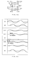
- Fig. 2a is a diagrammatic representation showing how a signal received through the first terminal 51 is directed to the third and fourth terminals 53, 54.
- Fig. 2b is a timing chart corresponding to Fig. 2a .
- the signal received through the first terminal 51 is directed to the third and fourth terminals 53, 54 as signals that are shifted in phase by 90 degrees from each other.
- the signal output through the fourth terminal 54 is delayed by 90 degrees with respect to the signal output through the third terminal 53.
- the power of the signals output through the third and fourth terminals 53, 54 is one half of the power of the signal supplied to the first terminal 51.
- Fig. 3a is a diagrammatic representation showing how the signals received through the third and fourth terminals 53, 54 are directed to the first and second terminals 51, 52.
- Fig. 3b is a timing chart corresponding to Fig. 3a .
- the signals are received through the third and fourth terminals 53, 54 when the two-state devices 6, 7 are in the impedance mismatched state. As apparent from the above, this occurs only during the transmission. Thus, the devices are generally in the state shown in Figs. 3a and 3b after the state shown in Figs. 2a and 2b .
- signals (3) and (4) are supplied to the third and fourth terminals 53, 54, respectively.
- the signals (3) and (4) in Fig. 3b are total reflections of the signals (3) and (4) in Fig. 2b .
- the signals (3) and (4) supplied to the third and fourth terminals 53, 54 are shifted in phase by 90 degrees from each other.
- the signal (4) is shifted in phase by another 90 degrees with respect to the signal (3).
- the signal (3) is directed into the first terminal 51 as a signal (3-1).
- the signal (4) which is delayed in phase by 90 degrees, is directed to the first terminal 51 as a signal (4-1).
- the signals (3) and (4) already have a 90-degree phase difference to which another 90-degree phase difference is added to produce the signals (3-1) and (4-1) to the 180-degree phase difference in total.
- the power of the signal (3) is identical to that of the signal (4).
- the power of the signal (3-1) is one half of the power of the signal (3) or (4) and is identical to that of the signal (4-1).
- the signals (3-1) and (4-1) are cancelled out each other because they are in antiphase and have the same power, so that no signal is directed to the first terminal 51.
- the signal (3) has no phase difference with respect to the signal (4).
- the signal (3) is directed to the second terminal 52 as a signal (3-2) that is delayed in phase by 90 degrees.
- the signal (4) is directed to the second terminal 52 as a signal (4-2).
- the signal (4) is delayed in phase by 90 degrees with respect to the signal (3), and the signal (3) is delayed in phase by 90 degrees as the signal (3-2).
- the power of the signal (3) is identical to that of the signal (4).
- the power of the signal (3-2) is one half of the power of the signal (3) or (4) and is identical to the power of the signal (4-2) .
- the signal (3-2) and the signal (4-2) are in phase, and have the same power, so that a composite signal enhanced with each other is obtained from the second terminal 52.
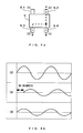
- Fig. 4a is a diagrammatic representation showing how the signal received through the second terminal 52 is output through the third and fourth terminals 53, 54.
- Fig. 4b is a timing chart corresponding to Fig. 4a .
- the signal received through the second terminal 52 is directed to the third and fourth terminals 53, 54 as signals shifted in phase by 90 degrees from each other.
- the signal output through the third terminal 53 is delayed by 90 degrees with respect to the signal output through the fourth terminal 54.
- the power of the signals output through the third and fourth terminals 53, 54 is one half of the power of the signal supplied to the first terminal 51.
- Figs. 5a through 5c and Figs. 6a and 6b are illustrative diagrams showing waveforms at major parts of the radar system 1 at transmission mode and reception mode. It should be noted that the delay time for each circuit is previously adjusted.
- the radar system 1 operates as follows at transmission mode.
- a millimeter-wave signal ( Fig. 5a ) generated by the high frequency oscillator 2 is supplied to the first terminal 51 of the 3 dB coupler 5.
- the pulse generator 8 brings the two-state devices 6, 7 into the impedance mismatched state because the operation mode is for transmission.
- the Schottky barrier diode in which the anode terminal is grounded and the cathode terminal is connected to the third and fourth terminals 53, 54 of the 3 dB coupler 5 is used for two-state device.
- the pulse signal ( Fig. 5b ) is supplied to the cathode terminal of the Schottky barrier diode.
- the pulse signal has a logic high level ( ⁇ T)
- the reverse bias is produced across the Schottky barrier diode to provide the impedance mismatched state.
- the millimeter-wave signal supplied to the first terminal 51 of the 3 dB coupler 5 is directed to the third and fourth terminals 53, 54, as shown in Figs. 2a and 2b .
- the millimeter-wave signals obtained through the third and fourth terminals 53, 54 are substantially totally reflected and signals supplied from the third and fourth terminals 53, 54 are directed to the first and second terminals 51, 52.
- the signal to the first terminal 51 is cancelled.
- the signal is output through the second terminal 52.
- the signal output through the second terminal 52 is supplied to the transmitting and receiving antenna 4 as a transmission signal.
- the transmitting and receiving antenna 4 emits the transmission signal as transmission waves ( Fig. 5c ). The transmission is thus performed.
- the waveform of the transmission wave is similar to the waveform obtained by modulating the millimeter-wave signal with the pulse signal.
- the radar system 1 serves as the pulse-type radar system.
- the radar system 1 operates as follows at reception mode.
- At least a part of the transmission waves ( Fig. 5c ) emitted during the operation at the time of transmission reflect from the obj ect as the reflectedwaves.
- the transmitting and receiving antenna 4 receives the reflected waves.
- the received reflected waves are supplied to the second terminal 52 of the 3 dB coupler 5 as a reception signal ( Fig. 6a ).
- R represents a distance from the transmitting and receiving antenna 4 to the object
- C represents a radio wave propagation velocity (ca. 3 x 10 8 m/s).
- the Schottky barrier diode in which the anode terminal is grounded and the cathode terminal is connected to the third and fourth terminals 53, 54 of the 3 dB coupler 5 is used for two-state device.
- the pulse signal is supplied to the cathode terminal of the Schottky barrier diode.
- the signal width of the pulse signal is smaller than ⁇ , so that it has a logic low level.
- the forward bias is produced across the Schottky barrier diode to provide the impedance matched state.
- the 3 dB coupler 5 supplies the reception signal to the third and fourth terminals 53, 54.
- the first terminal 51 of the 3 dB coupler 5 is provided with the millimeter-wave signal even at the time of reception.
- the millimeter-wave signal is, as described in conjunction with Figs. 2a and 2b , supplied to the third and fourth terminals 53, 54.
- the reception signal is subjected to homodyne detection by the millimeter-wave signal. Since the two-state devices 6, 7 are in the impedance matched state, the detected reception signal is directed to the third and fourth terminals 53 and 54 as high frequency signals for a Q channel and an I channel, respectively.
- the high frequency signal for the Q channel obtained from the third terminal 53 is supplied to the amplifier 10 via the capacitor 12 that breaks the direct current. It is then amplified by a predetermined amplification factor and is supplied through the output terminal 14 to the subsequent electronic circuit as a wave detection signal for the Q channel ( Fig. 6b ).
- the high frequency signal for the I channel obtained from the fourth terminal 54 is supplied to the amplifier 9 via the capacitor 11 that obstructs passage of the direct current. It is then amplified by a predetermined amplification factor and is supplied through the output terminal 13 to the subsequent electronic circuit as a wave detection signal for the I channel ( Fig. 6b ).
- the wave detection signals for the Q and I channels have a waveform as shown in Fig. 6b .
- Doppler beat is produced.
- the amplitude of the detected reception signal is determined depending on the phase relationships between the reception signal and the millimeter-wave signal supplied through the first terminal 51 of the 3 dB coupler 5. This is why a wave detection voltage is not determined at a certain point in Fig. 6b .
- no signal is supplied from the 3 dB coupler 5 to the amplifiers 9, 10 when the two-state devices 6, 7 are in the impedance mismatched state.
- the two-state devices 6, 7 are implemented with a Schottky barrier diode, a pulse signal is given and it is supplied to the amplifiers 9, 10 via the capacitors 11, 12, respectively. Accordingly, the voltage of the wave detection signal is determined depending on the pulse signal when the two-state devices 6, 7 are in the impedance mismatched state. In Fig. 6b , it is -10 V.
- the subsequent electronic circuit it is possible to determine the distance of the object, the traveling speed of the object, and the size of the object, from the wave detection signals for the Q and I channels.
- the distance to the object can be determined in the wave detection signal shown in Fig. 6b , by means of measuring the time duration between the time when the wave detection voltage is changed by the pulse signal and the time when the wave detection voltage is changed by the reception signal. Since the wave detection voltage by the pulse signal is quite different from the wave detection voltage by the reception signal, they can readily be distinguished according to the wave detection voltage.
- Fig. 7a is an illustrative diagram showing a Doppler beat signal obtained according to the wave detection signal for the I channel and the distance to the object.
- Fig. 7b is an illustrative diagram showing a Doppler beat signal obtained according to the wave detection signal for the Q channel and the distance to the object.
- the solid line represents the Doppler beat signal while the dashed line represents an envelope thereof.
- the traveling speedof the obj ect is determined according to the frequency of the Doppler beat signal for the I channel.
- Fig. 7c is an illustrative diagram showing a composite waveform of square mean values of the Doppler beat signal for the I channel and the Doppler beat signal for the Q channel.
- the amplitude represents reflectivity of the transmission waves from the object, which indicates the size of the object.
- the radar system 1 having the aforementioned configuration comprises a significantly less number of the component parts. This contributes to cost reduction and reduction in size.
- the system is simple in structure with a less number of component parts, so that it can be expected to improve the yields of good products.
- the high frequency oscillator is required to be a high-power one because it should supply the necessary power to both the transmission unit and the reception unit.
- an output signal from the single high frequency oscillator 2 is time divided and individually supplied to the transmission unit and the reception unit at the time of transmission and reception, respectively. This makes it possible to reduce the output power of the high frequency oscillator 2 as compared to the conventional ones, achieving more efficient power consumption of a smaller system at a lower cost.
- the present invention is not limited to the embodiment described above.
- the 3 dB coupler 5 used in the present embodiment as the four-terminal device may be replaced with other component having similar functions.
- a four-terminal hybrid coupler may be used.
Landscapes
- Engineering & Computer Science (AREA)
- Radar, Positioning & Navigation (AREA)
- Remote Sensing (AREA)
- Computer Networks & Wireless Communication (AREA)
- Physics & Mathematics (AREA)
- General Physics & Mathematics (AREA)
- Radar Systems Or Details Thereof (AREA)
Abstract
To provide a smaller radar system having a simple structure with as small number of component parts as possible at a lower cost as compared to conventional ones.
A radar system 1 including a 3 dB coupler 5 having four terminals, and a pulse generator 8. A first terminal 51 of the 3 dB coupler 5 is supplied with an output signal from a high frequency oscillator 2 while a second terminal 52 of the 3 dB coupler 5 is connected to a transmitting and receiving antenna 4. Third and fourth terminals 53 and 54 of the 3 dB coupler 5 are connected to two-state devices 6, 7, respectively, which are in impedance mismatched only for a predetermined period of time to totally reflect the signal from the 3 dB coupler 5 and are in impedance matched during the time period other than the predetermined time to direct a signal from the 3 dB coupler 5 to a subsequent electronic circuit. The pulse generator 8 causes the two-state devices 6, 7 to be impedance mismatched at the time of transmission and causes the two-state devices 6, 7 to be impedance matched at the time of reception.
Description
- The present invention relates to a radar system having a small detectable range, such as an on-vehicle millimeter-wave radar.
- A pulse-type radar system emits a sequence of pulses as transmission waves after being modulated to have a predetermined frequency and receives reflected waves which are reflections of the transmission waves from an object. The system then determines distance to the object by measuring the time it takes for the reflected waves to return. The pulse-type radar system uses high frequency signals in which different frequencies are used respectively for transmission and reception to determine a differential frequency as an intermediate frequency signal. The distance to the object is measured by means of calculating the time it takes for the intermediate frequency signal to have its maximum amplitude (Non-patent Document 1).
- Some pulse-type radar systems utilize heterodyne detection in which a high frequency oscillator is used for both the transmission unit and the reception unit. Heterodyne radars require a lot of millimeter-wave components such as a circulator or a directional coupler, to deal with millimeter-wave signals. Heterodyne radars use two high frequency oscillators and use a lot of millimeter-wave heterodyne radars, which limits miniaturization and cost reduction of the radar.
- Thus, some radars use a homodyne detector in which a signal from a single high frequency oscillator is modulated in a transmission unit and is also used for a frequency conversion in a reception unit. Homodyne radar systems share a signal from a single high frequency oscillator for both the transmission unit and the reception unit, so that they can be reduced in size and costs in comparison with heterodyne radar systems.
Patent Document 1 shows a homodyne pulse radar system. - Pulse radar according to the
Patent Document 1 emits a high frequency signal converted by means of ASK (amplitude shift keying) technique with a high speed square wave signal. The converted output is then reflected from an object as reflected wave. The reflected wave is used as a reception signal. Then logical AND operation is performed on the reception signal and a gating signal which is a delayed result of the high speed square wave signal. A delay time of the gating signal at which the maximum output level is obtained represents a delayed time of the reception signal. The distance to the object is calculated according to this delay time. - [Non-patent Document 1] Takashi YOSHIDA, "Radar Engineering Revised Edition", The Institute of Electronics, Information and Communication Engineers, October 1, 1996, p. 74-75 and p. 175-177.
- [Patent Document1]Japanese Patent Laid-open No.
2006-177983 - Conventional homodyne radar systems can be practically reduced in size and cost than heterodyne radar systems. However, even in the radar system according to the
Patent Document 1, there are two line units for both the transmission and reception. A number of parts are still required. This can complicate the structure or reduce the yield of good products. - An object of the present invention is to provide a smaller radar system with the reduced number of component parts as much as possible which can easily be structured at lower cost than in conventional systems.
- A radar system according to the present invention that solves the aforementioned problem has a 3 dB coupler or a four-terminal device having functions equivalent thereto, and a pulse generator. A first terminal of said four-terminal device is supplied with an output signal from a transmitting and receiving high frequency oscillator. A second terminal of said four-terminal device is connected to a transmitting and receiving antenna. A third terminal and a fourth terminal of said four-terminal device are connected to two-state devices, respectively, each of the two-state devices being adapted to totally reflect a signal from said four-terminal device when it is impedance mismatched only for a predetermined period of time, and to direct the signal from said four-terminal device to a subsequent electronic circuit during the time period other than the predeterminedperiodof time when it is impedance matched. Said pulse generator causes said two-state device to be impedance mismatched at the time of transmission and causes said two-state device to be impedance matched at the time of reception.
- At the time of transmission, a signal supplied from the high frequency oscillator through the first terminal is directed to the third terminal and the fourth terminal with a phase difference by 90 degrees, but no signal is directed to the second terminal. Since the two-state device is in impedance mismatched, the signals emitted to the third and fourth terminals are substantially totally reflected. However, the signals directed to the first terminal are cancelled when being composed, because of the 180-degree phase difference. The signals directed to the second terminal are composed in phase and directed to the antenna without being cancelled. The thus composite signal is emitted from the antenna. As used herein, the term "substantially totally reflected" refers to total reflection or near total reflection.
- At the time of reception, each of the two-state devices is in impedance matched, so that the signal received from the antenna through the second terminal is directed to the third and fourth terminals with a difference in phase by 90 degrees.
- The signal received from the antenna is subjected to homodyne detection by using an output from the high frequency oscillator supplied through the first terminal from, for example, the high frequency oscillator. A high frequency signal for a Q channel is obtained from the third terminal while a high frequency signal for an I channel is obtained from the fourth terminal.
- Said pulse generator may cause said two-state devices to be impedance mismatched when a signal capable of conveying binary digits has either value and cause said two-state devices to be impedance matched when the signal has the other value. With this configuration, the radar system operates as transmission mode when the signal capable of conveying binary digits has either value, and operates reception mode when the signal has the other value.
- According to the present invention, the four-terminal device and the two-state devices are used to change the signal paths either for transmission or reception. This makes it possible to provide a simple radar system with a less number of component parts as compared to conventional ones, reducing size and cost of the radar system. In addition, the system is simple in structure with a less number of component parts, so that it can be expected to improve the yields of good products.
-
-
Fig. 1 is a configuration diagram showing a radar system according to the present embodiment; -
Fig. 2a is a diagrammatic representation showing how a signal received through a first terminal is emitted through third and fourth terminals; -
Fig. 2b is a timing chart corresponding toFig. 2a ; -
Fig. 3a is a diagrammatic representation showing how signals received through third and fourth terminals are emitted through the first and second terminals; -
Fig. 3b is a timing chart corresponding toFig. 3a ; -
Fig. 4a is a diagrammatic representation showing how a signal received through a second terminal is emitted through third and fourth terminals; -
Fig. 4b is a timing chart corresponding toFig. 4a -
Fig. 5a is an illustrative diagram showing a waveform of a millimeter-wave signal; -
Fig. 5b is an illustrative diagram showing a waveform of a pulse signal; -
Fig. 5c is an illustrative diagram showing a transmission waveform; -
Fig. 6a is an illustrative diagram showing a waveform of a reception signal; -
Fig. 6b is an illustrative diagram showing a waveform of a detected signal; -
Fig. 7a is an illustrative diagram showing a Doppler beat signal for an I channel; -
Fig. 7b is an illustrative diagram showing a Doppler beat signal for a Q channel; and -
Fig. 7c is an illustrative diagram showing a composite waveform of square mean values of the Doppler beat signal for the I channel and the Doppler beat signal for the Q channel. - Now, an embodiment inwhich the present invention is applied to a radar system using millimeter-wave band is described in detail with reference to the drawings.
-
Fig. 1 is a configuration diagram showing aradar system 1 according to the present embodiment. - The
radar system 1 comprises ahigh frequency oscillator 2 for transmission and reception, a transmitting and receivingantenna 4, a 3dB coupler 5, two-state devices pulse generator 8,amplifiers capacitors 11, 12, andoutput terminals dB coupler 5, the two-state devices pulse generator 8 are contained in a same container or housing. Thisradar system 1 can be used as, for example, a short-range radar that can be mounted on a vehicle. A reception signal obtained from theradar system 1 is supplied to a subsequent electronic circuit (not shown) through theoutput terminals - The highfrequency oscillator2generates a millimeter-wave signal and supplies it to the 3
dB coupler 5. The millimeter-wave signal is used for emission at the time of transmission and is used for homodyne detection at the time of reception. - The transmitting and receiving
antenna 4 emits, as transmission waves, a transmission signal supplied from the 3dB coupler 5 at the time of transmission. At the time of reception, it receives reflected waves generated when the transmission waves reflect from the object. The reflected waves are supplied to the 3dB coupler 5 as a reception signal. - The 3
dB coupler 5 is a very small four-terminal device which can easily be mounted on a substrate in the container or the housing. It comprises first throughfourth terminals 51 to 54. Signals received through thefirst terminal 51 and thesecond terminal 52 are output through thethird terminal 53 and thefourth terminal 54, respectively, as signals shifted in phase by 90 degrees from each other and having power that is one half of the original. Likewise, signals received through thethird terminal 53 and thefourth terminal 54 are output through thefirst terminal 51 and thesecond terminal 52, respectively, as signals shifted in phase by 90 degrees from each other and having power that is one half of the original. No signal is exchanged between thefirst terminal 51 and thesecond terminal 52, and between thethird terminal 53 and thefourth terminal 54. - The
first terminal 51 is supplied with a millimeter-wave signal from thehigh frequency oscillator 2. Thesecond terminal 52 is connected to the transmitting and receivingantenna 4. At the time of transmission, thesecond terminal 52 sends a transmission signal to the transmitting and receivingantenna 4. At the time of reception, thesecond terminal 52 is supplied with a reception signal from the transmitting and receivingantenna 4. The third andfourth terminals state devices - The two-
state devices fourth terminals dB coupler 5. The two-state devices pulse generator 8 generates pulses representing two states for controlling the impedance condition of the two-state devices - When the two-
state devices fourth terminals dB coupler 5 are supplied to theamplifiers state devices fourth terminals dB coupler 5 are substantially totally reflected. This state represents transmission mode. - In order to change the impedance states between transmission and reception, the
pulse generator 8 controls the impedance state by using a signal capable of conveying binary digits (hereinafter, referred to as a "pulse signal"). For example, thepulse generator 8 uses the pulse signal to turn the two-state devices state devices - In this embodiment, the
pulse generator 8 is directly connected to the two-state devices pulse generator 8 may be provided in the circuit at any different positions as long as it is connected to the two-state devices dB coupler 5 via direct-current connection. With this configuration, thepulse generator 8 may be connected to thefirst terminal 51 of the 3dB coupler 5. - The two-
state devices pulse generator 8 serves to apply an appropriate voltage to the anode terminal and the cathode terminal of the Schottky barrier diode to establish and break electrical continuity. For example, the pulse signal is supplied to the cathode terminal of the Schottky barrier diode in which the anode terminal is grounded and the cathode terminal is connected to the third andfourth terminals dB coupler 5. When the pulse signal has a logic low level, the forward bias is produced across the Schottky barrier diode, which establishes electrical continuity to provide the impedance matched state. When the pulse signal has a logic high level, the reverse bias is produced across the Schottky barrier diode, which breaks the electrical continuity into the impedance mismatched state. - The
amplifiers fourth terminals dB coupler 5 by a predetermined amplification factor to send the amplified signals to the subsequent electronic circuit. Thecapacitors 11, 12 block the DC component of the signals supplied through the third andfourth terminals amplifiers - Next, detailed operation of the 3
dB coupler 5 is described. -
Fig. 2a is a diagrammatic representation showing how a signal received through thefirst terminal 51 is directed to the third andfourth terminals Fig. 2b is a timing chart corresponding toFig. 2a . The signal received through thefirst terminal 51 is directed to the third andfourth terminals fourth terminal 54 is delayed by 90 degrees with respect to the signal output through thethird terminal 53. The power of the signals output through the third andfourth terminals first terminal 51. -
Fig. 3a is a diagrammatic representation showing how the signals received through the third andfourth terminals second terminals Fig. 3b is a timing chart corresponding toFig. 3a . The signals are received through the third andfourth terminals state devices Figs. 3a and 3b after the state shown inFigs. 2a and 2b . - In
Figs. 3a and 3b , signals (3) and (4) are supplied to the third andfourth terminals Fig. 3b are total reflections of the signals (3) and (4) inFig. 2b . Thus, the signals (3) and (4) supplied to the third andfourth terminals - At the
first terminal 51, the signal (4) is shifted in phase by another 90 degrees with respect to the signal (3). For example, the signal (3) is directed into thefirst terminal 51 as a signal (3-1). The signal (4), which is delayed in phase by 90 degrees, is directed to thefirst terminal 51 as a signal (4-1). The signals (3) and (4) already have a 90-degree phase difference to which another 90-degree phase difference is added to produce the signals (3-1) and (4-1) to the 180-degree phase difference in total. In addition, the power of the signal (3) is identical to that of the signal (4). The power of the signal (3-1) is one half of the power of the signal (3) or (4) and is identical to that of the signal (4-1). The signals (3-1) and (4-1) are cancelled out each other because they are in antiphase and have the same power, so that no signal is directed to thefirst terminal 51. - At the
second terminal 52, the signal (3) has no phase difference with respect to the signal (4). For example, the signal (3) is directed to thesecond terminal 52 as a signal (3-2) that is delayed in phase by 90 degrees. The signal (4) is directed to thesecond terminal 52 as a signal (4-2). The signal (4) is delayed in phase by 90 degrees with respect to the signal (3), and the signal (3) is delayed in phase by 90 degrees as the signal (3-2). This means that the signal (3-2) is in phase with respect to the signal (4-2). In addition, the power of the signal (3) is identical to that of the signal (4). The power of the signal (3-2) is one half of the power of the signal (3) or (4) and is identical to the power of the signal (4-2) . The signal (3-2) and the signal (4-2) are in phase, and have the same power, so that a composite signal enhanced with each other is obtained from thesecond terminal 52. -
Fig. 4a is a diagrammatic representation showing how the signal received through thesecond terminal 52 is output through the third andfourth terminals Fig. 4b is a timing chart corresponding toFig. 4a . The signal received through thesecond terminal 52 is directed to the third andfourth terminals third terminal 53 is delayed by 90 degrees with respect to the signal output through thefourth terminal 54. The power of the signals output through the third andfourth terminals first terminal 51. - Operation of the
radar system 1 with the aforementioned configuration is described with reference toFigs. 5a through 5c andFigs. 6a and 6b .Figs. 5a through 5c andFigs. 6a and 6b are illustrative diagrams showing waveforms at major parts of theradar system 1 at transmission mode and reception mode. It should be noted that the delay time for each circuit is previously adjusted. - The
radar system 1 operates as follows at transmission mode. - First, a millimeter-wave signal (
Fig. 5a ) generated by thehigh frequency oscillator 2 is supplied to thefirst terminal 51 of the 3dB coupler 5. Thepulse generator 8 brings the two-state devices fourth terminals dB coupler 5 is used for two-state device. The pulse signal (Fig. 5b ) is supplied to the cathode terminal of the Schottky barrier diode. When the pulse signal has a logic high level (ΔT), the reverse bias is produced across the Schottky barrier diode to provide the impedance mismatched state. The millimeter-wave signal supplied to thefirst terminal 51 of the 3dB coupler 5 is directed to the third andfourth terminals Figs. 2a and 2b . - Because the two-
state devices fourth terminals fourth terminals second terminals Figs. 3a and 3b , in this case, the signal to thefirst terminal 51 is cancelled. On the other hand, the signal is output through thesecond terminal 52. The signal output through thesecond terminal 52 is supplied to the transmitting and receivingantenna 4 as a transmission signal. The transmitting and receivingantenna 4 emits the transmission signal as transmission waves (Fig. 5c ). The transmission is thus performed. It should be noted that the waveform of the transmission wave is similar to the waveform obtained by modulating the millimeter-wave signal with the pulse signal. Theradar system 1 serves as the pulse-type radar system. - The
radar system 1 operates as follows at reception mode. - First, at least a part of the transmission waves (
Fig. 5c ) emitted during the operation at the time of transmission reflect from the obj ect as the reflectedwaves. The transmitting and receivingantenna 4 receives the reflected waves. The received reflected waves are supplied to thesecond terminal 52 of the 3dB coupler 5 as a reception signal (Fig. 6a ). - The reception signal is delayed by τ= 2R/C seconds with respect to the transmission waves, wherein R represents a distance from the transmitting and receiving
antenna 4 to the object, and C represents a radio wave propagation velocity (ca. 3 x 10⁸ m/s). When the impedance state of the two-state devices pulse generator 8, the two-state devices dB coupler 5 if τ is larger than the signal width ΔT of the pulse signal. For example, the Schottky barrier diode in which the anode terminal is grounded and the cathode terminal is connected to the third andfourth terminals dB coupler 5 is used for two-state device. The pulse signal is supplied to the cathode terminal of the Schottky barrier diode. The signal width of the pulse signal is smaller than τ, so that it has a logic low level. Thus, the forward bias is produced across the Schottky barrier diode to provide the impedance matched state. - As described in conjunction with
Figs. 4a and 4b , the 3dB coupler 5 supplies the reception signal to the third andfourth terminals first terminal 51 of the 3dB coupler 5 is provided with the millimeter-wave signal even at the time of reception. The millimeter-wave signal is, as described in conjunction withFigs. 2a and 2b , supplied to the third andfourth terminals state devices fourth terminals - The high frequency signal for the Q channel obtained from the
third terminal 53 is supplied to theamplifier 10 via thecapacitor 12 that breaks the direct current. It is then amplified by a predetermined amplification factor and is supplied through theoutput terminal 14 to the subsequent electronic circuit as a wave detection signal for the Q channel (Fig. 6b ). - The high frequency signal for the I channel obtained from the
fourth terminal 54 is supplied to theamplifier 9 via the capacitor 11 that obstructs passage of the direct current. It is then amplified by a predetermined amplification factor and is supplied through theoutput terminal 13 to the subsequent electronic circuit as a wave detection signal for the I channel (Fig. 6b ). - The wave detection signals for the Q and I channels have a waveform as shown in
Fig. 6b . - In the homodyne detection, Doppler beat is produced. The amplitude of the detected reception signal is determined depending on the phase relationships between the reception signal and the millimeter-wave signal supplied through the
first terminal 51 of the 3dB coupler 5. This is why a wave detection voltage is not determined at a certain point inFig. 6b . In addition, as to the wave detection signal, no signal is supplied from the 3dB coupler 5 to theamplifiers state devices state devices amplifiers capacitors 11, 12, respectively. Accordingly, the voltage of the wave detection signal is determined depending on the pulse signal when the two-state devices Fig. 6b , it is -10 V. - In the subsequent electronic circuit, it is possible to determine the distance of the object, the traveling speed of the object, and the size of the object, from the wave detection signals for the Q and I channels.
- The distance to the object can be determined in the wave detection signal shown in
Fig. 6b , by means of measuring the time duration between the time when the wave detection voltage is changed by the pulse signal and the time when the wave detection voltage is changed by the reception signal. Since the wave detection voltage by the pulse signal is quite different from the wave detection voltage by the reception signal, they can readily be distinguished according to the wave detection voltage. -
Fig. 7a is an illustrative diagram showing a Doppler beat signal obtained according to the wave detection signal for the I channel and the distance to the object.Fig. 7b is an illustrative diagram showing a Doppler beat signal obtained according to the wave detection signal for the Q channel and the distance to the object. InFigs. 7a and 7b , the solid line represents the Doppler beat signal while the dashed line represents an envelope thereof. The traveling speedof the obj ect is determined according to the frequency of the Doppler beat signal for the I channel. -
Fig. 7c is an illustrative diagram showing a composite waveform of square mean values of the Doppler beat signal for the I channel and the Doppler beat signal for the Q channel. The amplitude represents reflectivity of the transmission waves from the object, which indicates the size of the object. - The
radar system 1 having the aforementioned configuration comprises a significantly less number of the component parts. This contributes to cost reduction and reduction in size. In addition, the system is simple in structure with a less number of component parts, so that it can be expected to improve the yields of good products. - Conventional homodyne radar systems use an output signal from a single high frequency oscillator is used for the transmission and reception. Therefore, the high frequency oscillator is required to be a high-power one because it should supply the necessary power to both the transmission unit and the reception unit. In the present embodiment, an output signal from the single
high frequency oscillator 2 is time divided and individually supplied to the transmission unit and the reception unit at the time of transmission and reception, respectively. This makes it possible to reduce the output power of thehigh frequency oscillator 2 as compared to the conventional ones, achieving more efficient power consumption of a smaller system at a lower cost. - It should be understood that the present invention is not limited to the embodiment described above. For example, the 3
dB coupler 5 used in the present embodiment as the four-terminal device may be replaced with other component having similar functions. For example, a four-terminal hybrid coupler may be used.
Claims (4)
- A radar system comprising a 3 dB coupler or a four-terminal device having functions equivalent thereto, and a pulse generator,
a first terminal of said four-terminal device being supplied with an output signal from a transmitting and receiving high frequency oscillator;
a second terminal of said four-terminal device being connected to a transmitting and receiving antenna,
a third terminal and a fourth terminal of said four-terminal device being connected to two-state devices, respectively, each of the two-state devices being adapted to totally reflect a signal from said four-terminal device when it is impedance mismatched only for a predetermined period of time, and to direct the signal from said four-terminal device to a subsequent electronic circuit during the time period other than the predetermined period of time when it is impedance matched,
said pulse generator being adapted to cause:
said two-state device to be impedance mismatched at the time of transmission and said two-state device to be impedance matched at the time of reception. - The radar system as claimed in Claim 1, wherein a reception signal from said antenna is subjected to homodyne detection by an output signal from said high frequency oscillator and the detected wave output is emitted through said third terminal and said fourth terminal at the time of reception.
- The radar system as claimed in Claim 1 or 2, wherein said four-terminal devices, said pulse generator and said two-state devices are contained in a single housing.
- The radar system as claimed in Claim 1, wherein said pulse generator causes said two-state devices to be impedance mismatched when a signal capable of conveying binary digits has either value and causes said two-state devices to be impedance matched when the signal has the other value.
Applications Claiming Priority (2)
| Application Number | Priority Date | Filing Date | Title |
|---|---|---|---|
| JP2007091358A JP2008249498A (en) | 2007-03-30 | 2007-03-30 | Radar system |
| PCT/JP2008/054249 WO2008126539A1 (en) | 2007-03-30 | 2008-03-04 | Radar device |
Publications (2)
| Publication Number | Publication Date |
|---|---|
| EP2141509A1 true EP2141509A1 (en) | 2010-01-06 |
| EP2141509A4 EP2141509A4 (en) | 2011-03-30 |
Family
ID=39863695
Family Applications (1)
| Application Number | Title | Priority Date | Filing Date |
|---|---|---|---|
| EP08721665A Withdrawn EP2141509A4 (en) | 2007-03-30 | 2008-03-04 | Radar device |
Country Status (4)
| Country | Link |
|---|---|
| US (1) | US8111188B2 (en) |
| EP (1) | EP2141509A4 (en) |
| JP (1) | JP2008249498A (en) |
| WO (1) | WO2008126539A1 (en) |
Cited By (1)
| Publication number | Priority date | Publication date | Assignee | Title |
|---|---|---|---|---|
| US8111188B2 (en) * | 2007-03-30 | 2012-02-07 | Yokowo Co., Ltd | Radar system |
Families Citing this family (2)
| Publication number | Priority date | Publication date | Assignee | Title |
|---|---|---|---|---|
| JP5781346B2 (en) * | 2011-03-28 | 2015-09-24 | 株式会社ヨコオ | Radar equipment |
| CN103237079A (en) * | 2013-04-30 | 2013-08-07 | 鸿富锦精密工业(深圳)有限公司 | Remote control device, and method and system for intelligently downloading and installing remote control software |
Family Cites Families (23)
| Publication number | Priority date | Publication date | Assignee | Title |
|---|---|---|---|---|
| US3237130A (en) * | 1963-04-17 | 1966-02-22 | Emerson Electric Co | Four-port directional coupler with direct current isolated intermediate conductor disposed about inner conductors |
| US3525993A (en) * | 1968-05-03 | 1970-08-25 | Chain Lakes Research Asociates | Direction responsive vehicle speed measuring police radar apparatus |
| DE2158793B2 (en) * | 1971-11-26 | 1975-04-10 | Messerschmitt-Boelkow-Blohm Gmbh, 8000 Muenchen | Device for measuring and displaying the distance and / or the change in distance between a motor vehicle and an obstacle |
| FR2286391A1 (en) * | 1974-09-27 | 1976-04-23 | Snecma | SHORT DISTANCE RADAR |
| JPS5828548B2 (en) * | 1975-08-29 | 1983-06-16 | 三菱電機株式会社 | Micro-Hatouchi |
| US4065768A (en) * | 1975-07-01 | 1977-12-27 | Mitsubishi Denki Kabushiki Kaisha | Radar apparatus |
| JPS5832348B2 (en) * | 1975-08-29 | 1983-07-12 | 三菱電機株式会社 | Micro-Hatouchi |
| US6225943B1 (en) * | 1978-05-01 | 2001-05-01 | Raytheon Company | Method of operating pulse radar |
| US4207547A (en) * | 1978-11-01 | 1980-06-10 | The United States Of America As Represented By The Secretary Of The Air Force | Reflection mode notch filter |
| US4286260A (en) * | 1979-09-11 | 1981-08-25 | E-Systems, Inc. | Ranging quadrature doppler microwave intrusion alarm system |
| US4521779A (en) * | 1980-04-24 | 1985-06-04 | The United States Of America As Represented By The Secretary Of The Navy | Pulse compression system |
| US4492960A (en) * | 1982-01-18 | 1985-01-08 | The United States Of America As Represented By The Secretary Of The Navy | Switching mixer |
| GB2181007A (en) * | 1985-09-27 | 1987-04-08 | Philips Electronic Associated | Distributed amplifier load arrangements |
| GB2246678A (en) * | 1990-07-30 | 1992-02-05 | Philips Electronic Associated | Cw radar system. |
| DE4203932A1 (en) * | 1992-02-11 | 1993-08-12 | Deutsche Aerospace | SEND / RECEIVE MODULE |
| DE19610850C1 (en) * | 1996-03-19 | 1997-04-24 | Siemens Ag | Monostatic homodyne radar system for vehicle radar and radar sensor, e.g. for level measurement |
| US6426716B1 (en) * | 2001-02-27 | 2002-07-30 | Mcewan Technologies, Llc | Modulated pulse doppler sensor |
| US6930631B2 (en) * | 2001-11-28 | 2005-08-16 | M/A-Com, Inc. | Sensor front-end with phase coding capability |
| US6639543B2 (en) * | 2002-01-09 | 2003-10-28 | Tyco Electronics Corp. | Sensor front-end for vehicle closing velocity sensor |
| JP3998601B2 (en) * | 2002-10-09 | 2007-10-31 | 富士通株式会社 | Pulse radar equipment |
| DE102005008733A1 (en) * | 2004-02-26 | 2005-10-13 | Kyocera Corp. | Transceiver antenna, isolator, high frequency oscillator and the same high frequency transmitter / receiver |
| JP4068113B2 (en) | 2006-03-28 | 2008-03-26 | 富士通株式会社 | Pulse radar apparatus and distance detection method thereof |
| JP2008249498A (en) * | 2007-03-30 | 2008-10-16 | Yokowo Co Ltd | Radar system |
-
2007
- 2007-03-30 JP JP2007091358A patent/JP2008249498A/en active Pending
-
2008
- 2008-03-04 US US12/594,121 patent/US8111188B2/en not_active Expired - Fee Related
- 2008-03-04 WO PCT/JP2008/054249 patent/WO2008126539A1/en not_active Ceased
- 2008-03-04 EP EP08721665A patent/EP2141509A4/en not_active Withdrawn
Cited By (1)
| Publication number | Priority date | Publication date | Assignee | Title |
|---|---|---|---|---|
| US8111188B2 (en) * | 2007-03-30 | 2012-02-07 | Yokowo Co., Ltd | Radar system |
Also Published As
| Publication number | Publication date |
|---|---|
| US8111188B2 (en) | 2012-02-07 |
| WO2008126539A1 (en) | 2008-10-23 |
| EP2141509A4 (en) | 2011-03-30 |
| US20100134347A1 (en) | 2010-06-03 |
| JP2008249498A (en) | 2008-10-16 |
Similar Documents
| Publication | Publication Date | Title |
|---|---|---|
| CN102866387B (en) | Millimeter wave frequency modulated continuous wave (FMCW) two-unit phased array distance and velocity measurement monolithic radar transceiver | |
| US11486999B2 (en) | Radar system comprising a plurality of radar chips | |
| CN1906500B (en) | Small-size low-power-consumption short-range radar and control method thereof | |
| EP2798369B1 (en) | Radar system providing multiple waveforms for long range and short range target detection | |
| US6426716B1 (en) | Modulated pulse doppler sensor | |
| US7432847B2 (en) | Ultra-wideband transceiver | |
| US20080297400A1 (en) | Monostatic Planar Multi-Beam Radar Sensor | |
| JP4573518B2 (en) | Object position determination method, object range and orientation measurement method, and object range and orientation measurement sensor | |
| CN1349612A (en) | Device for detecting objects in the area surroundiong a vehicle | |
| CN203287518U (en) | Frequency-modulated continuous wave transmitting and receiving module | |
| US20030100285A1 (en) | Sensor front-end with phase coding capability | |
| JP2005515445A (en) | Sensor front end for vehicle approach speed sensor | |
| CN105445706B (en) | With frequency noise jamming compensation device and X-band single antenna continuous-wave radar system | |
| CN111638504B (en) | Continuous wave radar front end | |
| US8111188B2 (en) | Radar system | |
| US7443336B2 (en) | In-vehicle pulse radar device | |
| CN114063010A (en) | Detection chip, detection device and detection method based on SOC technology | |
| KR100979284B1 (en) | Radar transmitter receiver | |
| KR102842342B1 (en) | Coherent multi-static radar system for vehicle use | |
| US5266956A (en) | Method and device for the measurement of short distances by analysis of the delay in the propagation of a wave | |
| US20060220947A1 (en) | Compact low power consumption microwave distance sensor obtained by power measurement on a stimulated receiving oscillator | |
| CN216771962U (en) | Detection chip and detection device based on SOC technique | |
| EP1184678A2 (en) | Radar transceiver | |
| US7274922B2 (en) | Circuit arrangement for generating an IQ-signal | |
| US4682174A (en) | Moving target indicator using a surface acoustic wave device |
Legal Events
| Date | Code | Title | Description |
|---|---|---|---|
| PUAI | Public reference made under article 153(3) epc to a published international application that has entered the european phase |
Free format text: ORIGINAL CODE: 0009012 |
|
| 17P | Request for examination filed |
Effective date: 20091022 |
|
| AK | Designated contracting states |
Kind code of ref document: A1 Designated state(s): AT BE BG CH CY CZ DE DK EE ES FI FR GB GR HR HU IE IS IT LI LT LU LV MC MT NL NO PL PT RO SE SI SK TR |
|
| DAX | Request for extension of the european patent (deleted) | ||
| A4 | Supplementary search report drawn up and despatched |
Effective date: 20110228 |
|
| 17Q | First examination report despatched |
Effective date: 20111011 |
|
| STAA | Information on the status of an ep patent application or granted ep patent |
Free format text: STATUS: THE APPLICATION IS DEEMED TO BE WITHDRAWN |
|
| 18D | Application deemed to be withdrawn |
Effective date: 20120222 |