EP2140547B1 - Rf re-entrant combiner - Google Patents
Rf re-entrant combiner Download PDFInfo
- Publication number
- EP2140547B1 EP2140547B1 EP07855615.6A EP07855615A EP2140547B1 EP 2140547 B1 EP2140547 B1 EP 2140547B1 EP 07855615 A EP07855615 A EP 07855615A EP 2140547 B1 EP2140547 B1 EP 2140547B1
- Authority
- EP
- European Patent Office
- Prior art keywords
- combiner
- conductor arrangement
- dielectric
- intermediate conductor
- transmission lines
- Prior art date
- Legal status (The legal status is an assumption and is not a legal conclusion. Google has not performed a legal analysis and makes no representation as to the accuracy of the status listed.)
- Active
Links
Images


Classifications
-
- H—ELECTRICITY
- H01—ELECTRIC ELEMENTS
- H01P—WAVEGUIDES; RESONATORS, LINES, OR OTHER DEVICES OF THE WAVEGUIDE TYPE
- H01P5/00—Coupling devices of the waveguide type
- H01P5/12—Coupling devices having more than two ports
-
- H—ELECTRICITY
- H01—ELECTRIC ELEMENTS
- H01P—WAVEGUIDES; RESONATORS, LINES, OR OTHER DEVICES OF THE WAVEGUIDE TYPE
- H01P1/00—Auxiliary devices
- H01P1/20—Frequency-selective devices, e.g. filters
- H01P1/213—Frequency-selective devices, e.g. filters combining or separating two or more different frequencies
-
- H—ELECTRICITY
- H01—ELECTRIC ELEMENTS
- H01P—WAVEGUIDES; RESONATORS, LINES, OR OTHER DEVICES OF THE WAVEGUIDE TYPE
- H01P5/00—Coupling devices of the waveguide type
- H01P5/12—Coupling devices having more than two ports
- H01P5/16—Conjugate devices, i.e. devices having at least one port decoupled from one other port
- H01P5/18—Conjugate devices, i.e. devices having at least one port decoupled from one other port consisting of two coupled guides, e.g. directional couplers
- H01P5/184—Conjugate devices, i.e. devices having at least one port decoupled from one other port consisting of two coupled guides, e.g. directional couplers the guides being strip lines or microstrips
- H01P5/185—Edge coupled lines
Definitions
- Embodiments are described herein for electronic devices that can be used to couple and/or combine high-power electrical signals in the RF or microwave range.
- Power combiners and directional couplers are passive microwave devices that can be used to combine electrical signals in the Radio Frequency (RF) range (i.e. frequencies in the range of about 3 - 300 MHz) or microwave frequency range (i.e. frequencies above about 300 MHz).
- Power combiners can be used in amplifier modules that comprise multiple unit amplifiers. For instance, an amplifier module may include four unit amplifiers and the output of each unit amplifier can be combined together using a 4:1 combiner to produce the required total output power of the amplifier module.
- US3,237,130 describes a four-port directional coupler with direct current isolated intermediate conductor disposed about inner conductors.
- US2003/132816 describes a microstrip coupler.
- US4,459,568 describes an air-stripline overlay hybrid coupler.
- the capacitive portions may have a varying width for varying the odd mode electrical length for a range of frequencies.
- the combiner may further comprise four dielectric blocks, each of the dielectric blocks being in thermal communication with a surface of the first and second transmission lines exterior of the intermediate conductor arrangement and the outer conductor arrangement.
- the combiner may further comprise at least one additional dielectric block in thermal communication with the intermediate conductor arrangement and the outer conductor arrangement.
- the combiner may further comprise two additional dielectric blocks, each of which is in thermal communication with a surface of the intermediate conductor arrangement and the outer conductor arrangement.
- the dielectric material is made from at least one Boron-Nitride loaded Teflon and beryllium oxide selected according to dielectric constant requirements for the combiner.
- the at least one additional dielectric block is made from at least one of alumina, steatite, beryllium oxide, aluminium nitride, and a liquid low loss dielectric.
- the capacitive portions can be located on each end portion of both the third and fourth strip conductors. Also, at least one of the capacitive portions is a stub.
- the dielectric material may fill the region.
- the outer conductor arrangement may comprise fifth and sixth parallel strip conductors disposed above and below the third and fourth conductors defining a second region containing the third and fourth strip conductors, and additional dielectric material disposed between fourth and sixth parallel strip conductors.
- the dielectric material and the additional dielectric material can include one of ceramic-loaded Teflon, fibreglass reinforced Teflon, and glass-reinforced hydrocarbon/ceramic laminate selected according to dielectric constant requirements for the combiner.
- the combiner may further comprise a third dielectric portion disposed between the fourth conductor strip and the outer conductor arrangement.
- a chain combiner may be provided comprising a plurality of combiners connected in series.
- the combiner 10 includes a housing having an upper portion 12 (i.e. cover), and a lower portion 14 (i.e. a base), a plurality of ports 16-22, two transmission lines 24 and 26, and a floating intermediate conductor 28.
- the upper and lower portions 12 and 14 of the housing are conductive and provide an outer conductor arrangement as well as an electrical ground for the combiner 10.
- the floating intermediate conductor 28 provides an intermediate conductor arrangement for the combiner 10.
- the ports 16-22 are standard N connectors (50 ohm). However, other suitable connectors may also be used.
- the combiner 10 also includes shield elements 46 and 48 connected to ground to prevent parasitic coupling between the portion of the transmission lines 24 and 26 that are outside of the intermediate conductor 28.
- the transmission line 24 includes thick strip conductors 30 and 32 and a coaxial conductor portion 34.
- the transmission line 26 includes thick strip conductor portions 36 and 38 and a coaxial conductor portion 40.
- the particular thickness to be used for any conductor in any particular application is selected based upon a variety of factors including, but not limited to, the heat transfer characteristic required for the particular application, the frequency of operation, the desired characteristic impedances of the transmission lines and mechanical constraints/requirements. Those of ordinary skill in the art will appreciate how to assess the relevant factors and select a particular thickness.
- the coaxial conductor portions 34 and 40 within the intermediate conductor 28 have a length of one-quarter wavelength with regards to the operating frequency of the combiner 10.
- the thick strip conductor portions 30, 32, 36 and 38 almost resemble square coaxial conductors and are spaced from the surfaces of the upper and lower portions 12 and 14 of the housing by a certain distance for maintaining a suitable impedance match along these portions of the transmission lines 24 and 26.
- the thick strip conductor portions 30, 32, 36 and 38 have a low loss, good thermal conduction, and can handle a large amount of peak power (in theory in excess of 90 kW).
- the coaxial conductor portions 34 and 40 can be replaced with thick strip conductors.
- the thick strip conductor portions 30, 32, 36 and 38 can be replaced with coaxial conductors. However, this results in the ground plane separation in these portions of the transmission lines 24 and 26 being much lower than in the stripline case, which decreases the peak power capability.
- the floating intermediate conductor 28 is tubular in nature and includes channels for receiving the coaxial conductor portions 34 and 40 in a concentric fashion.
- the channels of the intermediate conductor 28 also receive dielectric materials 42 and 44, which are disposed about the coaxial conductor portions 34 and 40.
- the dielectric material 42 and 44 have a cylindrical shape with a circular bore to accommodate the coaxial conductors 34 and 40; i.e. the dielectric material 42 and 44 both have a sleeve-like form.
- the intermediate conductor 28 is electrically insulated from the outer conductor arrangement.
- the intermediate conductor 28 is also insulated from the transmission lines 24 and 26.
- the intermediate conductor 28 is shielding the coaxial conductor portions 34 and 40 from each other.
- an additional transmission line between the intermediate conductor 28 and the outer conductor arrangement which is in series with the two transmission lines 24 and 26 and acts as a mutual coupling medium.
- the cross-sectional shape of the floating intermediate conductor 28 can be round, elliptic or any other suitable shape.
- the dielectric material 42 and 44 may not form continuous sleeves.
- the dielectric materials 42 and 44 can include several small cylindrical pieces that are spaced apart from one another or one cylinder having holes. Many different arrangements can be suitable in this regard. Ceramic cylinders can also be used for the dielectric materials provided that the heat transfer properties are sufficient for high power applications.
- the combiner 10 provides coupling between RF signals provided to the transmission lines 24 and 26.
- ports 16 and 20 can act as an input port and an output port, respectively, for transmission line 24.
- ports 18 and 22 can act as a coupled port and an isolated port, respectively, for transmission line 26.
- An input signal at port 16 can be coupled to the port 18, such that the power of the input signal at port 16 is distributed between ports 18 and 20, while port 22 does not receive any power. The amount of signal distribution depends on the amount coupling between the transmission lines 24 and 26.
- input signals can be provided to both ports 16 and 18, such that the combined power from these input signals are provided to the port 20, while port 22 does not receive any power.
- the even and odd mode propagation constants also known as the even and odd mode propagation velocities
- the propagation velocities can be determined in terms of even and odd mode characteristic impedances.
- the even mode characteristic impedance Z oe is measured with respect to one of the inner coaxial conductor portions and the outer conductor arrangement when the magnitude and phase of the RF voltage and current of the coaxial conductor portions 34 and 40 are equal.
- the odd mode characteristic impedance Z oo is measured with respect to one of the inner coaxial conductor portions and the outer conductor arrangement when the RF voltage and current of the coaxial conductor portions 34 and 40 are equal in magnitude but 180 degrees out of phase.
- the characteristic impedance of the transmission line consisting of one of the inner transmission lines 24 or 26 and the intermediate conductor 28 is represented by Z o2 while the characteristic impedance of the transmission line between the outer conductor arrangement and one of the coaxial conductor portions is represented by Z o1 .
- the odd mode characteristic impedance Z oo is equal to Z o2 while the even mode characteristic impedance Z oe is equal to Z o2 + 2Z o1 .
- the characteristic impedances Z oe and Z oo are not equal for coupled conductors, and for tighter coupling such as 3 dB, there is a large difference between the characteristic impedances Z oe and Z oo .
- Those skilled in the art are knowledgeable in selecting values for the characteristic impedances Z oe and Z oo to achieve a certain amount of coupling between the transmission lines 24 and 26.
- the propagation velocity inside and outside the intermediate conductor 28 should be balanced, or at least as similar as is possible in practice.
- the propagation velocity (or propagation constant) in the transmission line defined above as Z oo which can be referred to as the odd mode propagation constant since it corresponds with odd mode excitation
- Z oe the propagation velocity (or propagation constant) in the transmission line defined above as Z oe
- One way to ensure this is to use the same dielectric material between the coaxial conductor portions and the intermediate conductor arrangement, and between the intermediate conductor arrangement and the outer conductor arrangement. Indeed, previous combiners have used only air as the dielectric in both of these regions so that the even and odd mode propagation constants are as similar as is practically possible.
- the combiner 10 utilizes the dielectric material 42 and 44 to provide enhanced thermal or heat transfer pathways for increased heat dissipation from the coaxial conductor portions 34 and 40 of the transmission lines 24 and 26. This enables the combiner 10 to handle higher power RF signals since any generated heat can be dissipated more quickly.
- the dielectric material 42 and 44 is made from a dielectric that has a good thermal conductivity.
- the dielectric material can be Boron-Nitride loaded Teflon, which has very good thermal conductivity.
- dielectric materials 42 and 44 can be used, like ceramics such as beryllium oxide (BeO) for example.
- BeO beryllium oxide
- the intermediate conductor 28 is modified to increase the electrical length of the transmission line Z oo such that directivity is preserved, i.e. the port 22 is isolated, even though the even and odd mode propagation constants appear to be unequal due to dielectric loading within the intermediate conductor 28. More specifically, the intermediate conductor 28 is modified by the addition of reactive loads.
- the reactive loads can be capacitive loads. Accordingly, the intermediate conductor 28 includes capacitive portions 50 to 56.
- a distributed capacitor has finite dimensions, hence a non-zero electrical length.
- the capacitive portions 50 to 56 are made with short lengths of a low impedance parallel plate transmission line. These parallel plate transmission lines can be considered to be in series with the transmission line Z oe , so the total electrical length of Z oe + 4 cap becomes equal with the electrical length of Z oo . In this way, the odd and even mode propagation velocities have been virtually equalized at least as much as is practically possible.
- a good starting point is that the intermediate conductor 28 must be longer by approximately the square root of the dielectric constant of the dielectric material used within the intermediate conductor 28.
- a 3D simulation program such as HFSS, CST or any other commercial or proprietary 3D simulator, known to those skilled in the art, can then be used to determine the amount of distributed capacitance that is required.
- the capacitive portions 50 to 56 have a semi-circular shape, which allows for creating a continuous variation of the total electrical length for Z oe in the plane that is perpendicular to the plane of the transmission lines 24 and 26. Accordingly, the compensation for electrical length in the even mode of propagation can be balanced over a certain frequency range. This means that for any frequency in the frequency range, an electrical length will exist across the capacitive portion in which the even and odd mode propagation velocities will be compensated. In alternative embodiments, different shapes can be used for the capacitive portions 50 to 56. However, the effect of compensation over a certain frequency range may no longer exist and there will be a lower bandwidth for electrical length compensation.
- each of the capacitive portions 50 to 56 do not have to be exactly the same, as long as the electrical length in the even and odd modes are equal.
- the combiner 10 further includes a plurality of dielectric blocks 58-72 which provide an enhanced thermal pathway between the portions of the transmission lines 24 and 26 that are external of the intermediate conductor 28, and the outer conductor arrangement.
- dielectric blocks 58-72 can be removed. However, in high power applications, all of the dielectric blocks 58-72 should be used.
- the dielectric blocks 58-72 can be made from similar material as the dielectric material 42 and 44. Direct physical contact between the dielectric blocks 58-72 and the outer conductor arrangement also provides a better heat transfer pathway, and is needed for very high power applications.
- FIG. 6 shown therein is a cross-sectional end view of another exemplary embodiment of a combiner 10' with the housing removed.
- the combiner 10' is similar to the combiner 10 but includes additional dielectric blocks 80 and 82.
- the combiner 10' can be used when there is a larger amount of RF power that is being coupled since the dielectric blocks 80 and 82 enable greater heat dissipation.
- the combiner 10 can be used as a 3 dB coupler, while the combiner 10' can be used as a 4.77 or 6 dB coupler.
- the dielectric blocks 80 and 82 are placed on either side of the intermediate conductor 28 and touch both the intermediate conductor 28 and the outer conductor arrangement to provide an enhanced thermal dissipation pathway between these structures.
- the dielectric blocks 80 and 82, and the dielectric blocks 58-72, can be made from Boron-Nitride loaded Teflon although other dielectrics can be used such as alumina, steatite, beryllium oxide, aluminum nitride and the like. Liquid low loss dielectrics can also be used, such as some silicones for example.
- the size of the dielectric blocks 80 and 82 can be varied depending on the amount of RF power being handled by the combiner 10'.
- the chain combiner 100 includes three couplers 102, 104 and 106, input ports 108, 110, 112, and 114 and an output port 116.
- the three couplers 102, 104 and 106 have different coupling factors due to the different amount of power that are being coupled.
- the coupler 102 can be a 3 dB coupler
- the coupler 104 can be a 4.77 dB coupler
- the coupler 106 can be a 6 dB coupler. Since the couplers 104 and 106 deal with a greater amount of RF power, these couplers employ the design of combiner 10' with the additional dielectric blocks on the intermediate conductor.
- the coupler 102 employs the design of the combiner 10.
- the coupler 102 includes input transmission lines 118 and 120, output transmission line 122 and an isolated transmission line 124.
- the coupler 104 includes input transmission lines 128 and 130, output transmission line 132 and an isolated transmission line 134.
- the coupler 106 includes input transmission lines 138 and 140, output transmission line 142 and an isolated transmission line 144.
- the output transmission line 122 of coupler 102 is electrically connected to the input transmission line 128 of coupler 104 via a connector 126.
- the output transmission line 132 of coupler 104 is electrically connected to the input transmission line 138 of coupler 106 via a connector 136.
- the output transmission line 142 of coupler 106 is electrically connected to the output port 116 via a connector 146.
- the chain combiner 100 uses couplers with designs similar to those of combiners 10 and 10', the chain combiner 100 has good wide band frequency performance while being able to accommodate high RF power. In one example, an implementation of the chain combiner 100 was able to combine signals with RF power in excess of 10 kW at the L-band.
- the couplers 104 and 106 of the chain combiner 100 require additional dielectric blocks because in the chain combiner 100, the incident RF power increases as the signals move toward the output 116 of the chain combiner 100.
- the coupler that combines the highest amount of power level i.e. the 6 dB coupler 106
- the coupler which needs the highest power dissipation capability i.e. the 6 dB coupler 106
- this particular design characteristic provides a favorable impedance change with a coupling value change.
- the concept of modifying a floating intermediate conductor by including capacitive loaded regions in a re-entrant coupler or combiner, to compensate for different odd and even mode propagation constants is not restricted to coax embodiments. This concept can also be extended to stripline and microstrip embodiments. In these cases, the use of a dielectric material with good thermal conductivity properties and a capacitively loaded floating intermediate conductor allows for the production of combiners with better heat dissipation characteristics, and hence higher power handling characteristics, as well as for much more design flexibility in selecting dielectric materials and heights for the substrates that are used.
- a stripline or microstrip combiner can be made using standard substrates. Also, because such a combiner can use wide transmission lines with characteristic impedances less than 50 ohm, the space between the transmission lines can be made larger than the substrate height and this kind of combiner can operate at much higher peak powers than other stripline or microstrip designs.
- the stripline or microstrip line versions of the modified combiner i.e. with a capacitively loaded intermediate conductor
- the combiner 150 includes transmission lines 152 and 154 in the form of a pair of parallel strip conductors in a common plane.
- the combiner 150 also includes another pair of parallel strip conductors 156 and 158 disposed above and below the strip conductors 152 and 154 in parallel planes.
- the strip conductors 156 and 158 provide an intermediate conductor arrangement that defines a first region that includes the strip conductors 156 and 158.
- the combiner 150 further includes a dielectric material 160 disposed within the region.
- the combiner 150 further includes strip conductors 162 and 164 disposed in parallel planes above and below the strip conductors 156 and 158.
- the strip conductors 162 and 164 provide an electrical ground and a housing for the combiner 150.
- the strip conductors 162 and 164 also provide an outer conductor arrangement for the combiner 150. Ports can be connected on each end of the transmission lines 152 and 154.
- the combiner 150 also includes a dielectric substrate layer 166 between the strip conductors 158 and 164.
- the strip conductor 156 includes capacitive portions 166, 168, 170 and 172 near each corner.
- the strip conductor 158 also includes corresponding capacitive portions 174, 176, 178 and 180 near each corner. Many other various types of shapes can be used for these capacitive portions.
- dielectric material that can be used for dielectrics 160 and 166 include, but are not limited to, ceramic-loaded Teflon, fiberglass reinforced Teflon, glass reinforced hydrocarbon/ceramic laminate, and the like.
- the dielectric ratio is not the correct required ratio, or some conductor width or other mechanical issue (i.e. ground spacing) becomes unpractical.
- capacitive loading is used in the microstrip case for the intermediate conductor, there is no need for specific dielectric constants. Different dielectric materials are still used, but by using capacitive loading for the intermediate conductor arrangement, a wide range of coupling values can be achieved using existing readily available dielectric materials.
- the combiner 200 includes transmission lines 202 and 204 in the form of a pair of parallel strip conductors in a common plane.
- the combiner 200 also includes another pair of parallel strip conductors 206 and 208 disposed above and below the strip conductors 202 and 204 in parallel planes.
- the strip conductors 206 and 208 provide an intermediate conductor arrangement that defines a first region that includes the strip conductors 202 and 204.
- the combiner 200 further includes several layers of dielectric materials shown in ghost lines in FIG. 10 .
- the combiner 200 includes a dielectric material 210 disposed within the first region about the strip conductors 202 and 204 and between the strip conductor 202 and 206.
- the combiner 200 also includes a layer of dielectric material 212 between the strip conductors 202 and 208, and another layer of dielectric material 214 beneath the strip conductor 208 (i.e. beneath the layer of dielectric material 212).
- the combiner 200 further includes a housing 216, which provides an outer conductor arrangement and an electrical ground for the combiner 200.
- the housing is shown as defined by a simulator. In practice, in a microstrip application, the housing is a milled pocket in a chassis to place the dielectric material 214. Further, the dielectric material 210 can be added only, i.e.
- the combiner 200 also includes a plurality of vias 218 and 220 to ground on both sides of the combiner 200 that includes input and output ports, as the case may be. Ports can be connected on each end of the transmission lines 202 and 204.
- the microstrip case depending on the coupling factor desired, a dielectric will also exist between the conductor 208 and ground but between the conductor 206 and the upper ground (i.e. upper portion of the housing) there is no need for a non-air dielectric.
- the microstrip case is also QUASI-TEM. For these two reasons, there is a significant difference in the propagation constant associated with the strip conductor 206 and the rest of the combiner 200. However, since conductors 206 and 208 are the equivalent of the floating intermediate conductor, it follows that by default the electrical length of the conductors 156 and 158 are the same.
- the strip conductor 206 includes capacitive loads 222-228 in the form of stubs near the end portions of each corner.
- the term "equalize" means that the odd and even mode electrical lengths are as similar to one another as is practically possible so that one of the ports of the combiner 200 is isolated.
- capacitive loading can be used on both the conductors 206 and 208 and in this case the amount of capacitive loading on each of these conductors can be different. Accordingly, capacitive loading provides a great degree of design flexibility and implementation for the microstrip case.
- the dielectric materials for the can be used for dielectrics 210, 212 and 214 include, but are not limited to, ceramic-loaded Teflon, fiberglass reinforced Teflon, glass reinforced hydrocarbon/ceramic laminate, and the like.
- the design simulator that is used can provide initial requirements for the dielectric constants of each of the dielectrics 210, 212 and 214, as is known by those skilled in the art.
- the next step in the design is to select the amount of capacitive loading that is required to equalize the electrical lengths as taught herein. Selection the amount of capacitive loading can also be varied to adjust the initial requirements for the dielectric constants to be more favorable.
- the various embodiments of the combiners described herein allow for the compensation of unequal odd and even mode propagation constants, which can result for different reasons, by using a capacitively loaded intermediate conductor arrangement. At least some of the embodiments described herein allow for the combination of high power RF signals in a small physical volume with low loss, have wide-band RF performance, good thermal dissipation capability, and insensitivity to misalignment/thermal expansion. Coupling is not sensitive to the small movements of the floating intermediate conductor within the combiner due to assembly errors or thermal expansion.
- the coax embodiments described herein have a high RF power capability for dealing with RF power far in excess of 10 kW peak or 1000 Watts on average due to the various heat dissipation paths that can be included in the combiner.
- a first improved heat dissipation path exists from the portion of the transmission lines that are enclosed within the intermediate conductor arrangement with the use of the dielectric material that is disposed about this portion of the transmission lines to provide a thermal path to the intermediate conductor arrangement.
- additional improved heat dissipation paths can be included between the intermediate conductor arrangement and the outer conductor arrangement by adding dielectric blocks or dielectric material between these two structures.
- a liquid low-loss dielectric material such as some silicones for example, can also be used to improve heat dissipation.
- At least the coax embodiments described herein also provide high bandwidth and combining efficiency.
- the peak and average power capability of the combiner increases very fast because the power goes up by the square of the voltage breakdown limit which is in direct relation with the actual dimensions.
- the combiner can have a peak power capability in the mega-Watt range. No other stripline/coax 3dB combiner can do this.
- the directivity and Voltage Standing Wave Ratio (VSWR) of the coaxial combiner are insensitive to thermal expansion.
- the bandwidth in which couplers can typically actually be used in practice as efficient combiners is determined by the return loss bandwidth and not by the coupling bandwidth since the return loss bandwidth is always narrower than the coupling bandwidth.
- the type of capacitive loading described herein for the various combiner embodiments does not restrict or deteriorate return loss bandwidth or return loss performance.
- the dielectric material added to the 50 ohm lines does not form any kind of reactive loading.
- the dielectric blocks used on the portion of the two transmission lines exterior to the intermediate conductor arrangement do not form any kind of reactive loading since the characteristic impedance is maintained at 50 ohms inside the dielectric blocks as well as outside.
- the dielectric introduced material disposed about the portion of the transmission lines internal to the intermediate conductor arrangement do not provide any reactive (i.e. capacitive) loading because the electrical length of the conductors is not reduced with respect to 90 degrees and because the characteristic impedance of these lines is not changed.
- the various embodiments for the combiner described herein can be used in practice for example from about 100 MHz up to about the X-band (i.e. 12,000 MHz). At frequencies lower than 1,000 MHz, the peak power capability can exceed 1 Megawatt in certain situations for certain embodiments excluding microstrip embodiments.
Landscapes
- Waveguides (AREA)
- Non-Reversible Transmitting Devices (AREA)
Description
- Embodiments are described herein for electronic devices that can be used to couple and/or combine high-power electrical signals in the RF or microwave range.
- Power combiners and directional couplers are passive microwave devices that can be used to combine electrical signals in the Radio Frequency (RF) range (i.e. frequencies in the range of about 3 - 300 MHz) or microwave frequency range (i.e. frequencies above about 300 MHz). Power combiners can be used in amplifier modules that comprise multiple unit amplifiers. For instance, an amplifier module may include four unit amplifiers and the output of each unit amplifier can be combined together using a 4:1 combiner to produce the required total output power of the amplifier module.
- With the advancement of transistor technology in the RF and microwave frequency ranges, it is now possible to generate higher RF power levels using semiconductor devices. Accordingly, a need exists for compact stripline/coaxial combiners that can reliably combine RF and microwave signals having power levels in the range of about 10 kW and above.
- However, current combiner technology that uses air suspended stripline or classic stripline/microstrip technology has insufficient thermal dissipation for the power levels which the combiner will be subjected to. In addition, the coupling performance of the combiners can be sensitive to thermal expansion and very sensitive to misalignment. Furthermore, waveguide technology is too large to be used in combiners for certain applications.
-
US3,237,130 describes a four-port directional coupler with direct current isolated intermediate conductor disposed about inner conductors.US2003/132816 describes a microstrip coupler.US4,459,568 describes an air-stripline overlay hybrid coupler. - The invention is defined in the claims to which reference is now directed.
- The capacitive portions may have a varying width for varying the odd mode electrical length for a range of frequencies.
- The combiner may further comprise four dielectric blocks, each of the dielectric blocks being in thermal communication with a surface of the first and second transmission lines exterior of the intermediate conductor arrangement and the outer conductor arrangement.
- The combiner may further comprise at least one additional dielectric block in thermal communication with the intermediate conductor arrangement and the outer conductor arrangement.
- The combiner may further comprise two additional dielectric blocks, each of which is in thermal communication with a surface of the intermediate conductor arrangement and the outer conductor arrangement.
- In at least some cases, the dielectric material is made from at least one Boron-Nitride loaded Teflon and beryllium oxide selected according to dielectric constant requirements for the combiner.
- In at least some cases, the at least one additional dielectric block is made from at least one of alumina, steatite, beryllium oxide, aluminium nitride, and a liquid low loss dielectric.
- More particularly, the capacitive portions can be located on each end portion of both the third and fourth strip conductors. Also, at least one of the capacitive portions is a stub.
- The dielectric material may fill the region.
- The outer conductor arrangement may comprise fifth and sixth parallel strip conductors disposed above and below the third and fourth conductors defining a second region containing the third and fourth strip conductors, and additional dielectric material disposed between fourth and sixth parallel strip conductors.
- The dielectric material and the additional dielectric material can include one of ceramic-loaded Teflon, fibreglass reinforced Teflon, and glass-reinforced hydrocarbon/ceramic laminate selected according to dielectric constant requirements for the combiner.
- The combiner may further comprise a third dielectric portion disposed between the fourth conductor strip and the outer conductor arrangement.
- A chain combiner may be provided comprising a plurality of combiners connected in series.
- For a better understanding of the embodiments described herein, and to show more clearly how they may be carried into effect, reference will now be made, by way of example only, to the accompanying drawings in which:
-
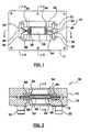
FIG. 1 is a top view of an exemplary embodiment of a combiner with the housing cover removed; -
FIG. 2 is a cross-sectional front view of the combiner ofFIG. 1 with the housing cover shown; -
FIG. 3 is a cross-sectional end view of the combiner ofFIG. 1 with the housing cover removed; -
FIG. 4 is another cross-sectional end view of the combiner ofFIG. 1 with the housing cover removed; -
FIG. 5 is a perspective view of the combiner ofFIG. 1 with the housing cover removed; -
FIG. 6 is a cross-sectional end view of another exemplary embodiment of a combiner with the housing removed; -
FIG. 7 is a perspective view of an exemplary embodiment of a 4:1 chain combiner; -
FIG. 8 is an end view of a portion of another exemplary embodiment of a combiner; -
FIG. 9 is a perspective view of a portion of the combiner ofFIG. 8 ; and -
FIG. 10 is a perspective view of another exemplary embodiment of a combiner. - It will be appreciated that for simplicity and clarity of illustration, where considered appropriate, reference numerals may be repeated among the figures to indicate corresponding or analogous elements or steps. In addition, numerous specific details are set forth in order to provide a thorough understanding of the exemplary embodiments described herein. However, it will be understood by those of ordinary skill in the art that the embodiments described herein may be practiced without these specific details. In other instances, well-known methods, procedures and components have not been described in detail since these are known to those skilled in the art.
- Referring now to
FIGS. 1-5 , shown therein are various views of an exemplary embodiment of acombiner 10. Thecombiner 10 includes a housing having an upper portion 12 (i.e. cover), and a lower portion 14 (i.e. a base), a plurality of ports 16-22, twotransmission lines 24 and 26, and a floatingintermediate conductor 28. The upper andlower portions combiner 10. The floatingintermediate conductor 28 provides an intermediate conductor arrangement for thecombiner 10. The ports 16-22 are standard N connectors (50 ohm). However, other suitable connectors may also be used. Thecombiner 10 also includesshield elements transmission lines 24 and 26 that are outside of theintermediate conductor 28. - The transmission line 24 includes
thick strip conductors coaxial conductor portion 34. Thetransmission line 26 includes thickstrip conductor portions coaxial conductor portion 40. The particular thickness to be used for any conductor in any particular application is selected based upon a variety of factors including, but not limited to, the heat transfer characteristic required for the particular application, the frequency of operation, the desired characteristic impedances of the transmission lines and mechanical constraints/requirements. Those of ordinary skill in the art will appreciate how to assess the relevant factors and select a particular thickness. Thecoaxial conductor portions intermediate conductor 28 have a length of one-quarter wavelength with regards to the operating frequency of thecombiner 10. The thickstrip conductor portions lower portions transmission lines 24 and 26. The thickstrip conductor portions coaxial conductor portions strip conductor portions transmission lines 24 and 26 being much lower than in the stripline case, which decreases the peak power capability. - The floating
intermediate conductor 28 is tubular in nature and includes channels for receiving thecoaxial conductor portions intermediate conductor 28 also receivedielectric materials coaxial conductor portions dielectric material coaxial conductors dielectric material intermediate conductor 28 is electrically insulated from the outer conductor arrangement. Theintermediate conductor 28 is also insulated from thetransmission lines 24 and 26. Also, there is no direct coupling between the twotransmission lines 24 and 26 and it appears that theintermediate conductor 28 is shielding thecoaxial conductor portions intermediate conductor 28 and the outer conductor arrangement, which is in series with the twotransmission lines 24 and 26 and acts as a mutual coupling medium. In alternative embodiments, the cross-sectional shape of the floatingintermediate conductor 28 can be round, elliptic or any other suitable shape. Furthermore, thedielectric material dielectric materials - In use, the
combiner 10 provides coupling between RF signals provided to thetransmission lines 24 and 26. For example,ports ports transmission line 26. An input signal atport 16 can be coupled to theport 18, such that the power of the input signal atport 16 is distributed betweenports port 22 does not receive any power. The amount of signal distribution depends on the amount coupling between thetransmission lines 24 and 26. Alternatively, input signals can be provided to bothports port 20, whileport 22 does not receive any power. In order to provide this behaviour, the even and odd mode propagation constants, also known as the even and odd mode propagation velocities, need to be balanced for thecombiner 10. The propagation velocities can be determined in terms of even and odd mode characteristic impedances. - The even mode characteristic impedance Zoe is measured with respect to one of the inner coaxial conductor portions and the outer conductor arrangement when the magnitude and phase of the RF voltage and current of the
coaxial conductor portions coaxial conductor portions inner transmission lines 24 or 26 and theintermediate conductor 28 is represented by Zo2 while the characteristic impedance of the transmission line between the outer conductor arrangement and one of the coaxial conductor portions is represented by Zo1. The odd mode characteristic impedance Zoo is equal to Zo2 while the even mode characteristic impedance Zoe is equal to Zo2 + 2Zo1. The characteristic impedances Zoe and Zoo are not equal for coupled conductors, and for tighter coupling such as 3 dB, there is a large difference between the characteristic impedances Zoe and Zoo. Those skilled in the art are knowledgeable in selecting values for the characteristic impedances Zoe and Zoo to achieve a certain amount of coupling between thetransmission lines 24 and 26. - In order to have an isolated port for the
combiner 10, the propagation velocity inside and outside theintermediate conductor 28 should be balanced, or at least as similar as is possible in practice. In other words, the propagation velocity (or propagation constant) in the transmission line defined above as Zoo, which can be referred to as the odd mode propagation constant since it corresponds with odd mode excitation, must be as similar as is practically possible with the propagation velocity (or propagation constant) in the transmission line defined above as Zoe, which can be referred to as the even mode propagation constant since it corresponds to even mode excitation. One way to ensure this is to use the same dielectric material between the coaxial conductor portions and the intermediate conductor arrangement, and between the intermediate conductor arrangement and the outer conductor arrangement. Indeed, previous combiners have used only air as the dielectric in both of these regions so that the even and odd mode propagation constants are as similar as is practically possible. - However, for combiners that have higher RF power requirements, it is not acceptable to use air as a dielectric since the thermal heat transfer characteristics of air are not suitable for use in high power applications. Rather, the
combiner 10 utilizes thedielectric material coaxial conductor portions transmission lines 24 and 26. This enables thecombiner 10 to handle higher power RF signals since any generated heat can be dissipated more quickly. Thedielectric material dielectric materials dielectric materials - However, by adding the
dielectric material intermediate conductor 28 is modified to increase the electrical length of the transmission line Zoo such that directivity is preserved, i.e. theport 22 is isolated, even though the even and odd mode propagation constants appear to be unequal due to dielectric loading within theintermediate conductor 28. More specifically, theintermediate conductor 28 is modified by the addition of reactive loads. The reactive loads can be capacitive loads. Accordingly, theintermediate conductor 28 includescapacitive portions 50 to 56. - To provide the
combiner 10 with higher power handling ability, distributed capacitive portions are used. However, a distributed capacitor has finite dimensions, hence a non-zero electrical length. In the exemplary embodiment, thecapacitive portions 50 to 56 are made with short lengths of a low impedance parallel plate transmission line. These parallel plate transmission lines can be considered to be in series with the transmission line Zoe, so the total electrical length of Zoe + 4cap becomes equal with the electrical length of Zoo. In this way, the odd and even mode propagation velocities have been virtually equalized at least as much as is practically possible. In order to estimate the actual amount of distributed capacitance that is required, a good starting point is that theintermediate conductor 28 must be longer by approximately the square root of the dielectric constant of the dielectric material used within theintermediate conductor 28. A 3D simulation program such as HFSS, CST or any other commercial or proprietary 3D simulator, known to those skilled in the art, can then be used to determine the amount of distributed capacitance that is required. - In this exemplary embodiment, the
capacitive portions 50 to 56 have a semi-circular shape, which allows for creating a continuous variation of the total electrical length for Zoe in the plane that is perpendicular to the plane of thetransmission lines 24 and 26. Accordingly, the compensation for electrical length in the even mode of propagation can be balanced over a certain frequency range. This means that for any frequency in the frequency range, an electrical length will exist across the capacitive portion in which the even and odd mode propagation velocities will be compensated. In alternative embodiments, different shapes can be used for thecapacitive portions 50 to 56. However, the effect of compensation over a certain frequency range may no longer exist and there will be a lower bandwidth for electrical length compensation. Further, the semi-circular shapes do not have to be perpendicular to the longitudinal axis of thecoax conductors capacitive portions 50 to 56 do not have to be exactly the same, as long as the electrical length in the even and odd modes are equal. - The
combiner 10 further includes a plurality of dielectric blocks 58-72 which provide an enhanced thermal pathway between the portions of thetransmission lines 24 and 26 that are external of theintermediate conductor 28, and the outer conductor arrangement. Depending on the power requirements of thecombiner 10, such as those that result from being used in a high peak power but low average power application, one or more or all of these dielectric blocks 58-72 can be removed. However, in high power applications, all of the dielectric blocks 58-72 should be used. The dielectric blocks 58-72 can be made from similar material as thedielectric material - Referring now to
FIG. 6 , shown therein is a cross-sectional end view of another exemplary embodiment of a combiner 10' with the housing removed. The combiner 10' is similar to thecombiner 10 but includes additional dielectric blocks 80 and 82. The combiner 10' can be used when there is a larger amount of RF power that is being coupled since the dielectric blocks 80 and 82 enable greater heat dissipation. For example, thecombiner 10 can be used as a 3 dB coupler, while the combiner 10' can be used as a 4.77 or 6 dB coupler. The dielectric blocks 80 and 82 are placed on either side of theintermediate conductor 28 and touch both theintermediate conductor 28 and the outer conductor arrangement to provide an enhanced thermal dissipation pathway between these structures. The dielectric blocks 80 and 82, and the dielectric blocks 58-72, can be made from Boron-Nitride loaded Teflon although other dielectrics can be used such as alumina, steatite, beryllium oxide, aluminum nitride and the like. Liquid low loss dielectrics can also be used, such as some silicones for example. The size of the dielectric blocks 80 and 82 can be varied depending on the amount of RF power being handled by the combiner 10'. - Referring now to
FIG. 7 , shown therein is a perspective view of an exemplary embodiment of a 4:1chain combiner 100 with the upper portion of the housing removed. Thechain combiner 100 includes threecouplers input ports output port 116. The threecouplers coupler 102 can be a 3 dB coupler, thecoupler 104 can be a 4.77 dB coupler and thecoupler 106 can be a 6 dB coupler. Since thecouplers coupler 102 employs the design of thecombiner 10. - The
coupler 102 includesinput transmission lines output transmission line 122 and anisolated transmission line 124. Thecoupler 104 includesinput transmission lines output transmission line 132 and an isolated transmission line 134. Thecoupler 106 includesinput transmission lines output transmission line 142 and an isolated transmission line 144. Theoutput transmission line 122 ofcoupler 102 is electrically connected to theinput transmission line 128 ofcoupler 104 via aconnector 126. Theoutput transmission line 132 ofcoupler 104 is electrically connected to theinput transmission line 138 ofcoupler 106 via aconnector 136. Finally, theoutput transmission line 142 ofcoupler 106 is electrically connected to theoutput port 116 via aconnector 146. - Since the
chain combiner 100 uses couplers with designs similar to those ofcombiners 10 and 10', thechain combiner 100 has good wide band frequency performance while being able to accommodate high RF power. In one example, an implementation of thechain combiner 100 was able to combine signals with RF power in excess of 10 kW at the L-band. - The
couplers chain combiner 100 require additional dielectric blocks because in thechain combiner 100, the incident RF power increases as the signals move toward theoutput 116 of thechain combiner 100. However, since the characteristic impedance of the intermediate conductor with respect to ground decreases as the coupling value is decreased, the coupler that combines the highest amount of power level (i.e. the 6 dB coupler 106) also has the lowest characteristic impedance for the intermediate conductor. Consequently, the coupler which needs the highest power dissipation capability (i.e. the 6 dB coupler 106), will have the shortest distance from the inner conductor to ground, and hence the shortest and best thermal path to ground. Accordingly, this particular design characteristic provides a favorable impedance change with a coupling value change. - The concept of modifying a floating intermediate conductor by including capacitive loaded regions in a re-entrant coupler or combiner, to compensate for different odd and even mode propagation constants is not restricted to coax embodiments. This concept can also be extended to stripline and microstrip embodiments. In these cases, the use of a dielectric material with good thermal conductivity properties and a capacitively loaded floating intermediate conductor allows for the production of combiners with better heat dissipation characteristics, and hence higher power handling characteristics, as well as for much more design flexibility in selecting dielectric materials and heights for the substrates that are used.
- For conventional reentrant combiners made using strip or microstrip designs, specific substrate heights must be used as well as dielectric materials having specific dielectric constants. This can be a serious limitation, since for a particular coupling factor value, dielectric materials with the specific required dielectric constant may not be readily available. However, using a capacitive loaded floating intermediate conductor, as is described herein, a stripline or microstrip combiner can be made using standard substrates. Also, because such a combiner can use wide transmission lines with characteristic impedances less than 50 ohm, the space between the transmission lines can be made larger than the substrate height and this kind of combiner can operate at much higher peak powers than other stripline or microstrip designs. The stripline or microstrip line versions of the modified combiner (i.e. with a capacitively loaded intermediate conductor) can also be used in a chain combiner.
- Referring now to
FIGS. 8 and 9 , shown therein is an end view and a perspective view of a portion of another exemplary embodiment of acombiner 150. Thecombiner 150 includestransmission lines combiner 150 also includes another pair ofparallel strip conductors strip conductors strip conductors strip conductors combiner 150 further includes adielectric material 160 disposed within the region. Thecombiner 150 further includesstrip conductors strip conductors strip conductors combiner 150. Thestrip conductors combiner 150. Ports can be connected on each end of thetransmission lines combiner 150 also includes adielectric substrate layer 166 between thestrip conductors - The fact that there is dielectric material between the
strip conductors strip conductors strip conductors strip conductors combiner 150 is isolated, the intermediate conductor arrangement is capacitively loaded. Accordingly, thestrip conductor 156 includescapacitive portions 166, 168, 170 and 172 near each corner. Thestrip conductor 158 also includes corresponding capacitive portions 174, 176, 178 and 180 near each corner. Many other various types of shapes can be used for these capacitive portions. This design also has the same wideband characteristic ascombiners 10 and 10' if the design properly balances the odd and even electrical lengths. The dielectric material that can be used fordielectrics - For conventional combiners having a microstrip design, the equality between the even and odd mode propagation velocities is lost. To mitigate the disparity, one approach can be to use dielectric materials with specific dielectric constants, which may not be readily available, to regain equality. However, the need for dielectric materials with specific dielectric constants, i.e. using different dielectric materials for each layer, and having a specific ratio of dielectric constants between different layers, is a design-limiting factor which is cumbersome. Hence the conventional microstrip approach is rarely used. Also, because of the required inter-relationship of the characteristic impedances, coupling values can be encountered in practice for which the readily available dielectric materials do not work i.e. the dielectric ratio is not the correct required ratio, or some conductor width or other mechanical issue (i.e. ground spacing) becomes unpractical. However, if capacitive loading is used in the microstrip case for the intermediate conductor, there is no need for specific dielectric constants. Different dielectric materials are still used, but by using capacitive loading for the intermediate conductor arrangement, a wide range of coupling values can be achieved using existing readily available dielectric materials.
- Referring now to
FIG. 10 , shown therein is a perspective view of another exemplary embodiment of acombiner 200. Thecombiner 200 includestransmission lines combiner 200 also includes another pair ofparallel strip conductors strip conductors strip conductors strip conductors combiner 200 further includes several layers of dielectric materials shown in ghost lines inFIG. 10 . Thecombiner 200 includes adielectric material 210 disposed within the first region about thestrip conductors strip conductor combiner 200 also includes a layer ofdielectric material 212 between thestrip conductors dielectric material 214 beneath the strip conductor 208 (i.e. beneath the layer of dielectric material 212). Thecombiner 200 further includes ahousing 216, which provides an outer conductor arrangement and an electrical ground for thecombiner 200. The housing is shown as defined by a simulator. In practice, in a microstrip application, the housing is a milled pocket in a chassis to place thedielectric material 214. Further, thedielectric material 210 can be added only, i.e. a piece cut to the desired dimension defined by the dimension ofstrip conductor 206 which also carriesconductor 206. In this case, thedielectric material 212 can act as the general substrate for the rest of the microstrip circuit. Thecombiner 200 also includes a plurality ofvias combiner 200 that includes input and output ports, as the case may be. Ports can be connected on each end of thetransmission lines - Accordingly, in the microstrip case, depending on the coupling factor desired, a dielectric will also exist between the
conductor 208 and ground but between theconductor 206 and the upper ground (i.e. upper portion of the housing) there is no need for a non-air dielectric. In addition, the microstrip case is also QUASI-TEM. For these two reasons, there is a significant difference in the propagation constant associated with thestrip conductor 206 and the rest of thecombiner 200. However, sinceconductors conductors conductors strip conductor 206, to equalize the electrical lengths associated with the even and odd mode, which is far easier to implement in practice. Accordingly, thestrip conductor 206 includes capacitive loads 222-228 in the form of stubs near the end portions of each corner. Please note that the term "equalize" means that the odd and even mode electrical lengths are as similar to one another as is practically possible so that one of the ports of thecombiner 200 is isolated. Furthermore, for specific coupling factors or dielectric constants, capacitive loading can be used on both theconductors dielectrics combiner 200, the design simulator that is used can provide initial requirements for the dielectric constants of each of thedielectrics - The various embodiments of the combiners described herein allow for the compensation of unequal odd and even mode propagation constants, which can result for different reasons, by using a capacitively loaded intermediate conductor arrangement. At least some of the embodiments described herein allow for the combination of high power RF signals in a small physical volume with low loss, have wide-band RF performance, good thermal dissipation capability, and insensitivity to misalignment/thermal expansion. Coupling is not sensitive to the small movements of the floating intermediate conductor within the combiner due to assembly errors or thermal expansion.
- In some circumstances, the coax embodiments described herein have a high RF power capability for dealing with RF power far in excess of 10 kW peak or 1000 Watts on average due to the various heat dissipation paths that can be included in the combiner. For instance, a first improved heat dissipation path exists from the portion of the transmission lines that are enclosed within the intermediate conductor arrangement with the use of the dielectric material that is disposed about this portion of the transmission lines to provide a thermal path to the intermediate conductor arrangement.
- In the coax case, if a greater amount of heat dissipation is required to deal with a larger amount of RF power, then additional improved heat dissipation paths can be included from the portion of the transmission lines that are external to the intermediate conductor arrangement by adding dielectric blocks or dielectric material to this region of the transmission lines to provide a better thermal path to the outer conductor arrangement. In fact, the highest electric field intensity is located at the region of the two transmission lines just external to the intermediate conductor arrangement. Accordingly, depending on the amount of RF power being handled by the combiner, it may be necessary to include dielectric material or dielectric blocks in this region.
- If an even greater amount of heat dissipation is required to deal with an even larger amount of RF power, then additional improved heat dissipation paths can be included between the intermediate conductor arrangement and the outer conductor arrangement by adding dielectric blocks or dielectric material between these two structures. In some embodiments, a liquid low-loss dielectric material, such as some silicones for example, can also be used to improve heat dissipation.
- At least the coax embodiments described herein also provide high bandwidth and combining efficiency. In fact, when the design operation frequency is decreased, the peak and average power capability of the combiner increases very fast because the power goes up by the square of the voltage breakdown limit which is in direct relation with the actual dimensions. For example, when designing the reentrant combiner according to the techniques provided herein, for the lower part of the UHF band or for the VHF band, the combiner can have a peak power capability in the mega-Watt range. No other stripline/coax 3dB combiner can do this. In addition, the directivity and Voltage Standing Wave Ratio (VSWR) of the coaxial combiner are insensitive to thermal expansion.
- In addition, the bandwidth in which couplers can typically actually be used in practice as efficient combiners is determined by the return loss bandwidth and not by the coupling bandwidth since the return loss bandwidth is always narrower than the coupling bandwidth. The type of capacitive loading described herein for the various combiner embodiments, does not restrict or deteriorate return loss bandwidth or return loss performance. Also, the dielectric material added to the 50 ohm lines does not form any kind of reactive loading. For instance, for the coax embodiments, the dielectric blocks used on the portion of the two transmission lines exterior to the intermediate conductor arrangement do not form any kind of reactive loading since the characteristic impedance is maintained at 50 ohms inside the dielectric blocks as well as outside. Further, the dielectric introduced material disposed about the portion of the transmission lines internal to the intermediate conductor arrangement do not provide any reactive (i.e. capacitive) loading because the electrical length of the conductors is not reduced with respect to 90 degrees and because the characteristic impedance of these lines is not changed.
- Furthermore, the various embodiments for the combiner described herein can be used in practice for example from about 100 MHz up to about the X-band (i.e. 12,000 MHz). At frequencies lower than 1,000 MHz, the peak power capability can exceed 1 Megawatt in certain situations for certain embodiments excluding microstrip embodiments.
Claims (14)
- A power combiner (10, 10', 150, 200) having four ports (16, 18, 20, 22), the combiner comprising:first and second transmission lines (24, 26, 152, 154, 202, 204) arranged side-by-side, each of the first and second transmission lines having a first end coupled to a respective one of four ports of the combiner and having a second end coupled to a respective one of four ports of the combiner;an intermediate conductor arrangement (28, 156, 158, 206, 208) disposed around the first and second transmission lines between the ports of the combiner and electrically insulated from the first and second transmission lines;an outer conductor arrangement (12, 14, 162, 164, 216) electrically insulated from the intermediate conductor arrangement at least partially by air; andheat transfer pathways extending along at least a portion of the length of the intermediate conductor arrangement, the heat transfer pathways being formed from a dielectric material (42, 44, 160, 210, 212) having good thermal conductivity disposed between the first transmission line and the intermediate conductor arrangement and between the second transmission line and the intermediate conductor arrangement, the dielectric material having a dielectric constant higher than that of air;the intermediate conductor arrangement having capacitive loads (50, 52, 54, 56, 166-172, 174-180, 222-228) to compensate for the imbalance in the odd and even mode propagation constants caused by the difference in the dielectric constants of a) the heat transfer pathways and b) the dielectric constant of the at least partial air insulation between the intermediate conductor arrangement and the outer conductor arrangement.
- The combiner of claim 1, wherein the capacitive loads (50, 52, 54, 56) are located near the ends of the intermediate conductor arrangement.
- The combiner of claim 1, wherein the first and second transmission lines comprise first and second coaxial conductor portions (34, 40), respectively, the heat transfer pathways are provided by dielectric material (42, 44) forming at least a partial sleeve around the first and second coaxial conductors (34, 40) respectively, and the intermediate conductor arrangement comprises two channels, each channel sized to receive a sleeved coaxial conductor.
- The combiner of any preceding claim, wherein the combiner (10) further comprises at least one dielectric block (58-72) on at least one surface of the first and second transmission lines (24, 26) exterior of the intermediate conductor arrangement (28), the at least one dielectric block being in thermal communication with the outer conductor arrangement (12,14).
- The combiner of claim 2, wherein the capacitive loads are semi-circular plates extending from end portions of the intermediate conductor arrangement at non-zero angles.
- The combiner of claim 2, wherein the capacitive loads have the same shape.
- The combiner of claim 4, wherein at least one of the at least one dielectric blocks is in thermal communication with the intermediate conductor arrangement and the outer conductor arrangement.
- The combiner of claim 3, wherein the first and second transmission lines further comprise thick strip conductor portions (30, 32 and 36, 38) electrically connected to the coaxial conductor portions (34 and 40).
- The combiner of any of claims 3-8, wherein the combiner further comprises shield elements disposed between the first and second transmission lines exterior of the intermediate conductor arrangement.
- The combiner of any preceding claim, wherein the outer conductor arrangement provides an electrical ground and forms a housing for the combiner.
- The combiner of claim 1, wherein the first and second transmission lines comprise first and second parallel strip conductors (152, 154) in a common plane, the intermediate conductor arrangement comprises third and fourth parallel strip conductors (156, 158) disposed above and below the first and second strip conductors (152, 154) and defining a region therebetween, the first and second strip conductors (152, 154) being contained within the region, and the dielectric material (160) being disposed within the region.
- The combiner of claim 11, wherein the capacitive loads are located near or on end portions of the third and fourth strip conductors (156, 158), wherein the third and fourth strip conductors are rectangular and the capacitive loads extend outward from sides of the third and fourth strip conductors near or on the end portions thereof within a common plane.
- The combiner of claim 1, wherein the first and second transmission lines comprise first and second parallel strip conductors (202, 204) in a common plane, the intermediate conductor arrangement comprises third and fourth parallel strip conductors (206, 208) disposed above and below the first and second strip conductors and defining a region therebetween, the first and second strip conductors being contained within the region, the heat transfer pathways comprises first and second dielectric portions (210, 212), the first dielectric portion (210) being disposed between the third conductor strip and the plane containing the first and second strip conductors, and the second dielectric portion (212) being disposed between the plane containing the first and second strip conductors and the fourth conductor strip.
- A chain reentrant combiner comprising a plurality of combiners according to any of the preceding claims, wherein the plurality of combiners are connected in series.
Applications Claiming Priority (2)
| Application Number | Priority Date | Filing Date | Title |
|---|---|---|---|
| US11/686,676 US7683734B2 (en) | 2007-03-15 | 2007-03-15 | RF re-entrant combiner |
| PCT/CA2007/002334 WO2008109979A1 (en) | 2007-03-15 | 2007-12-19 | Rf re-entrant combiner |
Publications (3)
| Publication Number | Publication Date |
|---|---|
| EP2140547A1 EP2140547A1 (en) | 2010-01-06 |
| EP2140547A4 EP2140547A4 (en) | 2010-09-01 |
| EP2140547B1 true EP2140547B1 (en) | 2016-10-12 |
Family
ID=39758938
Family Applications (1)
| Application Number | Title | Priority Date | Filing Date |
|---|---|---|---|
| EP07855615.6A Active EP2140547B1 (en) | 2007-03-15 | 2007-12-19 | Rf re-entrant combiner |
Country Status (4)
| Country | Link |
|---|---|
| US (1) | US7683734B2 (en) |
| EP (1) | EP2140547B1 (en) |
| CA (1) | CA2676680C (en) |
| WO (1) | WO2008109979A1 (en) |
Families Citing this family (6)
| Publication number | Priority date | Publication date | Assignee | Title |
|---|---|---|---|---|
| DE102010009104A1 (en) * | 2010-02-24 | 2011-08-25 | Epcos Ag, 81669 | detector circuit |
| US8638181B2 (en) * | 2010-08-20 | 2014-01-28 | Anaren, Inc. | Wideband balun using re-entrant coupled lines and ferrite material |
| ITMI20110708A1 (en) * | 2011-04-28 | 2012-10-29 | Com Tech S R L | UHF MULTI-CHANNEL FILTER |
| US9214899B2 (en) * | 2011-06-07 | 2015-12-15 | Telefonaktiebolaget L M Ericsson (Publ) | Power amplifier assembly comprising suspended strip lines |
| US9250317B1 (en) | 2012-12-20 | 2016-02-02 | Raytheon Canada Limited | Methods and apparatus for 3D radar data from 2D primary surveillance radar and passive adjunct radar |
| CN111799537A (en) * | 2020-06-29 | 2020-10-20 | 西南电子技术研究所(中国电子科技集团公司第十研究所) | Millimeter wave high-power ultra-wideband waveguide coupling device |
Family Cites Families (20)
| Publication number | Priority date | Publication date | Assignee | Title |
|---|---|---|---|---|
| US3327130A (en) * | 1960-09-15 | 1967-06-20 | Ibm | Tunnel diode polarity inverter |
| US3237130A (en) * | 1963-04-17 | 1966-02-22 | Emerson Electric Co | Four-port directional coupler with direct current isolated intermediate conductor disposed about inner conductors |
| US3593208A (en) | 1969-03-17 | 1971-07-13 | Bell Telephone Labor Inc | Microwave quadrature coupler having lumped-element capacitors |
| US3827001A (en) * | 1973-06-25 | 1974-07-30 | Us Navy | Wide band series-connected equal amplitude power divider |
| US4240051A (en) | 1979-06-29 | 1980-12-16 | Gte Laboratories Incorporated | High frequency power combiner or power divider |
| US4459568A (en) * | 1982-02-02 | 1984-07-10 | Rockwell International Corporation | Air-stripline overlay hybrid coupler |
| US5148132A (en) * | 1991-01-29 | 1992-09-15 | Sage Laboratories, Inc. | Microwave coupler |
| US5159298A (en) | 1991-01-29 | 1992-10-27 | Motorola, Inc. | Microstrip directional coupler with single element compensation |
| US5334958A (en) * | 1993-07-06 | 1994-08-02 | The United States Of America As Represented By The Secretary Of The Army | Microwave ferroelectric phase shifters and methods for fabricating the same |
| US6005442A (en) | 1996-03-26 | 1999-12-21 | Matsushita Electric Industrial Co., Ltd. | Divider/combiner |
| US5872491A (en) | 1996-11-27 | 1999-02-16 | Kmw Usa, Inc. | Switchable N-way power divider/combiner |
| US5796317A (en) | 1997-02-03 | 1998-08-18 | Tracor Aerospace Electronic Systems, Inc. | Variable impedance transmission line and high-power broadband reduced-size power divider/combiner employing same |
| US6275120B1 (en) * | 1998-04-09 | 2001-08-14 | Harris Corporation | Microstrip phase shifter having phase shift filter device |
| US6400235B1 (en) * | 1999-08-20 | 2002-06-04 | L3 Communications Corporation | Radio frequency, millimeter-wave or microwave device and method of making same |
| US6483397B2 (en) | 2000-11-27 | 2002-11-19 | Raytheon Company | Tandem six port 3:1 divider combiner |
| US6794954B2 (en) | 2002-01-11 | 2004-09-21 | Power Wave Technologies, Inc. | Microstrip coupler |
| JP2004040259A (en) * | 2002-06-28 | 2004-02-05 | Fujitsu Quantum Devices Ltd | Directional coupler and electronic apparatus employing the same |
| US6825738B2 (en) | 2002-12-18 | 2004-11-30 | Analog Devices, Inc. | Reduced size microwave directional coupler |
| US7026888B2 (en) | 2003-05-05 | 2006-04-11 | Marek Edward Antkowiak | Broadband non-directional tap coupler |
| US7429903B2 (en) * | 2006-03-24 | 2008-09-30 | R&D Microwaves Llc | Dual directional coupler with multi-stepped forward and reverse coupling rods |
-
2007
- 2007-03-15 US US11/686,676 patent/US7683734B2/en active Active
- 2007-12-19 CA CA2676680A patent/CA2676680C/en active Active
- 2007-12-19 EP EP07855615.6A patent/EP2140547B1/en active Active
- 2007-12-19 WO PCT/CA2007/002334 patent/WO2008109979A1/en not_active Ceased
Also Published As
| Publication number | Publication date |
|---|---|
| EP2140547A1 (en) | 2010-01-06 |
| WO2008109979A1 (en) | 2008-09-18 |
| CA2676680C (en) | 2014-09-23 |
| CA2676680A1 (en) | 2008-09-18 |
| EP2140547A4 (en) | 2010-09-01 |
| US20080224797A1 (en) | 2008-09-18 |
| US7683734B2 (en) | 2010-03-23 |
Similar Documents
| Publication | Publication Date | Title |
|---|---|---|
| US4129839A (en) | Radio frequency energy combiner or divider | |
| US6825738B2 (en) | Reduced size microwave directional coupler | |
| US20080048800A1 (en) | Low loss electrical delay line | |
| US9774069B2 (en) | N-way coaxial-to-coaxial combiner/divider | |
| US5410281A (en) | Microwave high power combiner/divider | |
| CA2676680C (en) | Rf re-entrant combiner | |
| US6542048B1 (en) | Suspended transmission line with embedded signal channeling device | |
| US4365215A (en) | High power coaxial power divider | |
| CN110212273A (en) | Two-frequency duplex device based on substrate integration wave-guide | |
| KR100897864B1 (en) | Power Divider with Coupling | |
| US10879577B2 (en) | Multilayer waveguide comprising at least one transition device between layers of this multilayer waveguide | |
| CN111048879B (en) | A broadband constant amplitude conversion structure from rectangular waveguide to double-terminal stripline | |
| TW202331752A (en) | Self supporting stripline structure | |
| US7023386B2 (en) | High gain antenna for microwave frequencies | |
| CN109378578B (en) | High Radiation Efficiency and High Gain Dielectric Resonant Antenna and Antenna Array on Silicon Substrate | |
| WO2001080347A1 (en) | Suspended transmission line with embedded amplifier | |
| US10177726B1 (en) | Waveguide to microstrip line N-port power splitter/combiner | |
| CN100365864C (en) | Improved directional coupler | |
| Van Messem et al. | Substrate integrated components for passive millimeterwave-frequency beamforming networks | |
| Ali et al. | Miniaturized grounded co-planar waveguide based x-band equal split Wilkinson power divider for aesa application | |
| JP7077137B2 (en) | Transmission lines and connectors | |
| CN115764226B (en) | A spaceborne power divider assembly | |
| Arshad et al. | 0 dB coupler employing slot technique on planar microstrip | |
| Tahara et al. | A novel three-port power divider with compensation networks for non-ideal isolation resistor | |
| CN115173016B (en) | Broadband 3dB branch line directional coupler |
Legal Events
| Date | Code | Title | Description |
|---|---|---|---|
| PUAI | Public reference made under article 153(3) epc to a published international application that has entered the european phase |
Free format text: ORIGINAL CODE: 0009012 |
|
| 17P | Request for examination filed |
Effective date: 20091015 |
|
| AK | Designated contracting states |
Kind code of ref document: A1 Designated state(s): AT BE BG CH CY CZ DE DK EE ES FI FR GB GR HU IE IS IT LI LT LU LV MC MT NL PL PT RO SE SI SK TR |
|
| DAX | Request for extension of the european patent (deleted) | ||
| A4 | Supplementary search report drawn up and despatched |
Effective date: 20100802 |
|
| RIC1 | Information provided on ipc code assigned before grant |
Ipc: H01P 5/18 20060101ALI20100727BHEP Ipc: H01P 1/213 20060101ALI20100727BHEP Ipc: H03H 7/46 20060101ALI20100727BHEP Ipc: H03H 7/48 20060101ALI20100727BHEP Ipc: H03H 7/00 20060101AFI20080929BHEP |
|
| 17Q | First examination report despatched |
Effective date: 20140306 |
|
| REG | Reference to a national code |
Ref country code: DE Ref legal event code: R079 Ref document number: 602007048324 Country of ref document: DE Free format text: PREVIOUS MAIN CLASS: H03H0007000000 Ipc: H01P0001213000 |
|
| RIC1 | Information provided on ipc code assigned before grant |
Ipc: H01P 5/18 20060101ALI20160316BHEP Ipc: H01P 5/12 20060101ALI20160316BHEP Ipc: H01P 1/213 20060101ALI20160316BHEP Ipc: H03H 7/48 20060101ALI20160316BHEP Ipc: H03H 7/46 20060101ALI20160316BHEP Ipc: H03H 7/00 20060101AFI20160316BHEP |
|
| GRAP | Despatch of communication of intention to grant a patent |
Free format text: ORIGINAL CODE: EPIDOSNIGR1 |
|
| RIC1 | Information provided on ipc code assigned before grant |
Ipc: H01P 5/18 20060101ALI20160420BHEP Ipc: H01P 1/213 20060101AFI20160420BHEP Ipc: H01P 5/12 20060101ALI20160420BHEP |
|
| INTG | Intention to grant announced |
Effective date: 20160504 |
|
| GRAS | Grant fee paid |
Free format text: ORIGINAL CODE: EPIDOSNIGR3 |
|
| GRAA | (expected) grant |
Free format text: ORIGINAL CODE: 0009210 |
|
| AK | Designated contracting states |
Kind code of ref document: B1 Designated state(s): AT BE BG CH CY CZ DE DK EE ES FI FR GB GR HU IE IS IT LI LT LU LV MC MT NL PL PT RO SE SI SK TR |
|
| REG | Reference to a national code |
Ref country code: GB Ref legal event code: FG4D |
|
| REG | Reference to a national code |
Ref country code: CH Ref legal event code: EP |
|
| REG | Reference to a national code |
Ref country code: AT Ref legal event code: REF Ref document number: 837238 Country of ref document: AT Kind code of ref document: T Effective date: 20161015 |
|
| REG | Reference to a national code |
Ref country code: IE Ref legal event code: FG4D |
|
| REG | Reference to a national code |
Ref country code: DE Ref legal event code: R096 Ref document number: 602007048324 Country of ref document: DE |
|
| REG | Reference to a national code |
Ref country code: FR Ref legal event code: PLFP Year of fee payment: 10 |
|
| REG | Reference to a national code |
Ref country code: LT Ref legal event code: MG4D |
|
| REG | Reference to a national code |
Ref country code: NL Ref legal event code: MP Effective date: 20161012 |
|
| PG25 | Lapsed in a contracting state [announced via postgrant information from national office to epo] |
Ref country code: LV Free format text: LAPSE BECAUSE OF FAILURE TO SUBMIT A TRANSLATION OF THE DESCRIPTION OR TO PAY THE FEE WITHIN THE PRESCRIBED TIME-LIMIT Effective date: 20161012 |
|
| REG | Reference to a national code |
Ref country code: AT Ref legal event code: MK05 Ref document number: 837238 Country of ref document: AT Kind code of ref document: T Effective date: 20161012 |
|
| PG25 | Lapsed in a contracting state [announced via postgrant information from national office to epo] |
Ref country code: SE Free format text: LAPSE BECAUSE OF FAILURE TO SUBMIT A TRANSLATION OF THE DESCRIPTION OR TO PAY THE FEE WITHIN THE PRESCRIBED TIME-LIMIT Effective date: 20161012 Ref country code: LT Free format text: LAPSE BECAUSE OF FAILURE TO SUBMIT A TRANSLATION OF THE DESCRIPTION OR TO PAY THE FEE WITHIN THE PRESCRIBED TIME-LIMIT Effective date: 20161012 Ref country code: GR Free format text: LAPSE BECAUSE OF FAILURE TO SUBMIT A TRANSLATION OF THE DESCRIPTION OR TO PAY THE FEE WITHIN THE PRESCRIBED TIME-LIMIT Effective date: 20170113 |
|
| PG25 | Lapsed in a contracting state [announced via postgrant information from national office to epo] |
Ref country code: AT Free format text: LAPSE BECAUSE OF FAILURE TO SUBMIT A TRANSLATION OF THE DESCRIPTION OR TO PAY THE FEE WITHIN THE PRESCRIBED TIME-LIMIT Effective date: 20161012 Ref country code: NL Free format text: LAPSE BECAUSE OF FAILURE TO SUBMIT A TRANSLATION OF THE DESCRIPTION OR TO PAY THE FEE WITHIN THE PRESCRIBED TIME-LIMIT Effective date: 20161012 Ref country code: IS Free format text: LAPSE BECAUSE OF FAILURE TO SUBMIT A TRANSLATION OF THE DESCRIPTION OR TO PAY THE FEE WITHIN THE PRESCRIBED TIME-LIMIT Effective date: 20170212 Ref country code: ES Free format text: LAPSE BECAUSE OF FAILURE TO SUBMIT A TRANSLATION OF THE DESCRIPTION OR TO PAY THE FEE WITHIN THE PRESCRIBED TIME-LIMIT Effective date: 20161012 Ref country code: BE Free format text: LAPSE BECAUSE OF FAILURE TO SUBMIT A TRANSLATION OF THE DESCRIPTION OR TO PAY THE FEE WITHIN THE PRESCRIBED TIME-LIMIT Effective date: 20161012 Ref country code: FI Free format text: LAPSE BECAUSE OF FAILURE TO SUBMIT A TRANSLATION OF THE DESCRIPTION OR TO PAY THE FEE WITHIN THE PRESCRIBED TIME-LIMIT Effective date: 20161012 Ref country code: PL Free format text: LAPSE BECAUSE OF FAILURE TO SUBMIT A TRANSLATION OF THE DESCRIPTION OR TO PAY THE FEE WITHIN THE PRESCRIBED TIME-LIMIT Effective date: 20161012 Ref country code: PT Free format text: LAPSE BECAUSE OF FAILURE TO SUBMIT A TRANSLATION OF THE DESCRIPTION OR TO PAY THE FEE WITHIN THE PRESCRIBED TIME-LIMIT Effective date: 20170213 |
|
| REG | Reference to a national code |
Ref country code: DE Ref legal event code: R097 Ref document number: 602007048324 Country of ref document: DE |
|
| PG25 | Lapsed in a contracting state [announced via postgrant information from national office to epo] |
Ref country code: SK Free format text: LAPSE BECAUSE OF FAILURE TO SUBMIT A TRANSLATION OF THE DESCRIPTION OR TO PAY THE FEE WITHIN THE PRESCRIBED TIME-LIMIT Effective date: 20161012 Ref country code: CZ Free format text: LAPSE BECAUSE OF FAILURE TO SUBMIT A TRANSLATION OF THE DESCRIPTION OR TO PAY THE FEE WITHIN THE PRESCRIBED TIME-LIMIT Effective date: 20161012 Ref country code: DK Free format text: LAPSE BECAUSE OF FAILURE TO SUBMIT A TRANSLATION OF THE DESCRIPTION OR TO PAY THE FEE WITHIN THE PRESCRIBED TIME-LIMIT Effective date: 20161012 Ref country code: EE Free format text: LAPSE BECAUSE OF FAILURE TO SUBMIT A TRANSLATION OF THE DESCRIPTION OR TO PAY THE FEE WITHIN THE PRESCRIBED TIME-LIMIT Effective date: 20161012 Ref country code: RO Free format text: LAPSE BECAUSE OF FAILURE TO SUBMIT A TRANSLATION OF THE DESCRIPTION OR TO PAY THE FEE WITHIN THE PRESCRIBED TIME-LIMIT Effective date: 20161012 |
|
| REG | Reference to a national code |
Ref country code: CH Ref legal event code: PL |
|
| PLBE | No opposition filed within time limit |
Free format text: ORIGINAL CODE: 0009261 |
|
| STAA | Information on the status of an ep patent application or granted ep patent |
Free format text: STATUS: NO OPPOSITION FILED WITHIN TIME LIMIT |
|
| PG25 | Lapsed in a contracting state [announced via postgrant information from national office to epo] |
Ref country code: BG Free format text: LAPSE BECAUSE OF FAILURE TO SUBMIT A TRANSLATION OF THE DESCRIPTION OR TO PAY THE FEE WITHIN THE PRESCRIBED TIME-LIMIT Effective date: 20170112 |
|
| 26N | No opposition filed |
Effective date: 20170713 |
|
| PG25 | Lapsed in a contracting state [announced via postgrant information from national office to epo] |
Ref country code: MC Free format text: LAPSE BECAUSE OF FAILURE TO SUBMIT A TRANSLATION OF THE DESCRIPTION OR TO PAY THE FEE WITHIN THE PRESCRIBED TIME-LIMIT Effective date: 20161012 |
|
| REG | Reference to a national code |
Ref country code: IE Ref legal event code: MM4A |
|
| PG25 | Lapsed in a contracting state [announced via postgrant information from national office to epo] |
Ref country code: LI Free format text: LAPSE BECAUSE OF NON-PAYMENT OF DUE FEES Effective date: 20161231 Ref country code: LU Free format text: LAPSE BECAUSE OF NON-PAYMENT OF DUE FEES Effective date: 20161219 Ref country code: CH Free format text: LAPSE BECAUSE OF NON-PAYMENT OF DUE FEES Effective date: 20161231 |
|
| REG | Reference to a national code |
Ref country code: FR Ref legal event code: PLFP Year of fee payment: 11 |
|
| PG25 | Lapsed in a contracting state [announced via postgrant information from national office to epo] |
Ref country code: IE Free format text: LAPSE BECAUSE OF NON-PAYMENT OF DUE FEES Effective date: 20161219 Ref country code: SI Free format text: LAPSE BECAUSE OF FAILURE TO SUBMIT A TRANSLATION OF THE DESCRIPTION OR TO PAY THE FEE WITHIN THE PRESCRIBED TIME-LIMIT Effective date: 20161012 |
|
| PG25 | Lapsed in a contracting state [announced via postgrant information from national office to epo] |
Ref country code: HU Free format text: LAPSE BECAUSE OF FAILURE TO SUBMIT A TRANSLATION OF THE DESCRIPTION OR TO PAY THE FEE WITHIN THE PRESCRIBED TIME-LIMIT; INVALID AB INITIO Effective date: 20071219 Ref country code: CY Free format text: LAPSE BECAUSE OF FAILURE TO SUBMIT A TRANSLATION OF THE DESCRIPTION OR TO PAY THE FEE WITHIN THE PRESCRIBED TIME-LIMIT Effective date: 20161012 |
|
| PG25 | Lapsed in a contracting state [announced via postgrant information from national office to epo] |
Ref country code: TR Free format text: LAPSE BECAUSE OF FAILURE TO SUBMIT A TRANSLATION OF THE DESCRIPTION OR TO PAY THE FEE WITHIN THE PRESCRIBED TIME-LIMIT Effective date: 20161012 |
|
| PG25 | Lapsed in a contracting state [announced via postgrant information from national office to epo] |
Ref country code: MT Free format text: LAPSE BECAUSE OF NON-PAYMENT OF DUE FEES Effective date: 20161219 |
|
| P01 | Opt-out of the competence of the unified patent court (upc) registered |
Effective date: 20230603 |
|
| PGFP | Annual fee paid to national office [announced via postgrant information from national office to epo] |
Ref country code: DE Payment date: 20251126 Year of fee payment: 19 |
|
| PGFP | Annual fee paid to national office [announced via postgrant information from national office to epo] |
Ref country code: GB Payment date: 20251119 Year of fee payment: 19 |
|
| PGFP | Annual fee paid to national office [announced via postgrant information from national office to epo] |
Ref country code: IT Payment date: 20251119 Year of fee payment: 19 |
|
| PGFP | Annual fee paid to national office [announced via postgrant information from national office to epo] |
Ref country code: FR Payment date: 20251120 Year of fee payment: 19 |