EP2138818B1 - Bolometer comprising an active layer surrounded on both sides by a contact layer and with an electrode layer. - Google Patents
Bolometer comprising an active layer surrounded on both sides by a contact layer and with an electrode layer. Download PDFInfo
- Publication number
- EP2138818B1 EP2138818B1 EP09162800.8A EP09162800A EP2138818B1 EP 2138818 B1 EP2138818 B1 EP 2138818B1 EP 09162800 A EP09162800 A EP 09162800A EP 2138818 B1 EP2138818 B1 EP 2138818B1
- Authority
- EP
- European Patent Office
- Prior art keywords
- layer
- layers
- bolometer
- contact
- groove
- Prior art date
- Legal status (The legal status is an assumption and is not a legal conclusion. Google has not performed a legal analysis and makes no representation as to the accuracy of the status listed.)
- Not-in-force
Links
Images



Classifications
-
- G—PHYSICS
- G01—MEASURING; TESTING
- G01J—MEASUREMENT OF INTENSITY, VELOCITY, SPECTRAL CONTENT, POLARISATION, PHASE OR PULSE CHARACTERISTICS OF INFRARED, VISIBLE OR ULTRAVIOLET LIGHT; COLORIMETRY; RADIATION PYROMETRY
- G01J5/00—Radiation pyrometry, e.g. infrared or optical thermometry
- G01J5/10—Radiation pyrometry, e.g. infrared or optical thermometry using electric radiation detectors
- G01J5/20—Radiation pyrometry, e.g. infrared or optical thermometry using electric radiation detectors using resistors, thermistors or semiconductors sensitive to radiation, e.g. photoconductive devices
-
- H—ELECTRICITY
- H10—SEMICONDUCTOR DEVICES; ELECTRIC SOLID-STATE DEVICES NOT OTHERWISE PROVIDED FOR
- H10N—ELECTRIC SOLID-STATE DEVICES NOT OTHERWISE PROVIDED FOR
- H10N19/00—Integrated devices, or assemblies of multiple devices, comprising at least one thermoelectric or thermomagnetic element covered by groups H10N10/00 - H10N15/00
Definitions
- the present invention relates to a semiconductor component comprising an active layer surrounded on both sides by a contact layer and with an electrode layer.
- the present invention can be used for different semiconductor components that have an extension in the plane of the layer that is greater than their dimension perpendicular to the said plane. It is exemplified in the description below, however, by a bolometer.
- US 5,998,791 shows a thermally sensitive element comprising a sensitive disc made from a carbonised sheet material. On top of said disc there is a conductive layer and the bottom of said disc there are two electrodes that are spaced apart in order to increase the resistance between the electrodes.
- a bolometer for example, is built up of a number of layers, which may, for example, be alternating layers of Si and layers of SiGe, which have an extension in the plane of the layers that is greater than their dimension perpendicular to this plane.
- the layers may also be GaAs/InGaAs or GaAs/ AlGaAs.
- An electrode layer is present on each of the two sides of such a structure, which electrode layer is connected to electrical conductors.
- a bolometer may be used, for example, as an IR detector element in a camera.
- the transport of current must take place vertically, i.e. across the plane of the layers, due to its construction as a multilayer structure with anisotropic properties.
- a limiting fact for such a structure is that the resistivity of the active layer cannot easily be freely chosen relative to other properties, such as, for example, temperature sensitivity.
- a number of detector elements is placed into a matrix in an imaging detector, where the CC-distances between the detector elements is determined by the optical design and by the cost of components.
- the electrical circuit that reads the detectors must be optimised relative to both the detector and the manufacturing process that is to be used.
- the present invention solves this problem and makes it possible to choose more easily the electrical properties independently of the geometrical dimensions.
- the present invention thus relates to a semiconductor component comprising a first, active, layer comprising one or several electrically conducting layers embedded on both sides by a first and a second layer respectively, which second first and second layers are contact layers, comprising one or several electrically conducting layers, where the active layer has an electrical conductivity that is lower than the conductivity in the contact layers, and where an electrode layer is present, connected to a first of the contact layers, and where the semiconductor component has greater dimensions in the lateral direction, i.e.
- the active layer is a thermistor layer comprising alternate quantum well layers or quantum dots and barrier layers in that each one of the electrodes on the upper contact layer has a surface area that is less than 10% of the surface area of the semiconductor component and in that the magnitude of the surface area of the upper contact layer relative to the magnitude of the upper surface area of the semiconductor component has been adapted to give the semiconductor component a predetermined electrical resistance.
- Figure 1 shows a semiconductor component 1 comprising a first, active, layer 3 comprising one or several electrically conducting layers embedded on both sides by a second layer, a contact layer 2, 4, comprising one or several electrically conducting layers.
- the active layer 3 has an electrical conductivity that is lower than the conductivity in the contact layers 2, 4.
- An electrode layer is present, not shown in the drawings, connected to at least one of the contact layers 2, 4.
- the electrode layers normally have an extension that is less than the extension of the contact layers.
- the semiconductor component 1 has greater dimensions in the lateral direction, i.e. in the plane of the layers, than it has in the direction perpendicular to this plane.
- the groove 7 passes through all layers 2, 3, 4 such that a lower 6 of the electrodes is exposed. This makes it possible for the component to be connected through the lower electrode 6 and the upper electrode 5.
- the electrical resistance between the two electrodes 5, 6 is thus determined by the resistivity of the active layer 3, the surface area of the electrodes, and the thickness of the active layer.
- the electrodes have an extension in the lateral direction that is less than the lateral dimensions of the semiconductor component. Furthermore, a groove 10; 14; 17 is present through at least the upper 2 of the contact layers. Furthermore, electrodes 8,9; 12,13; 15,16 are present on both sides of the groove, where it is intended that the semiconductor component be connected through the electrodes.
- the active layer 3 is a temperature-sensitive layer.
- the active layer 3 is a thermistor layer comprising alternate quantum well layers or quantum dots and barrier layers.
- the groove 10 passes through the upper layer 2 of the contact layers.
- an upper electrode 8, 9 is present on each side of the groove.
- two separate electrodes 8, 9 are formed on the same side of the component 1.
- the electrical current is spread over the complete area of one of the upper contact layers such that it flows down to the lower contact layer 4 and subsequently up to the second upper contact layer 19.
- the resistance in this embodiment will be approximately four times higher than it would be according to the embodiment shown in Figure 2 .
- the resistance still depends on the size of the pixels, i.e. the lateral size of the IR structure 1, which is determined by the optical properties.
- the detector material consists of a multilayer structure in which the electrical conductivity differs significantly between the contact layers 2, 4 and the active layer 3, and the fact that the lateral dimensions are significantly greater than the vertical dimensions, i.e. the dimensions perpendicular to the plane of the structure.
- the transport of current through the active layer 3 will be essentially limited to the volume that lies between the surrounding contact layers 2, 4. The region between these is inactive from an electrical point of view.
- the lateral dimensions of the structure in figure 3 may be 30 micrometers.
- the length of one edge of the square electrodes 8, 9 may be 3 micrometers.
- the upper contact layer has a surface area that is less than 10% of the surface area of the semiconductor component.
- Figure 4 shows a second embodiment of the invention.
- the groove 14 in this embodiment is relatively broad, which leads to the active volume being significantly lower than the volume according to the said second embodiment, with the consequence that the resistance is correspondingly higher.
- the surface area of the pixel is the same as previously. It is thus possible to optimise the resistance separately from the size of the pixel by adapting the area at the upper contact layer 2.
- the said groove 17 is designed such that a lattice of the upper contact layer is formed, which lattice is arranged to increase the optical absorption of incident light that impinges onto the semiconductor component.
- Figure 5 shows this third embodiment of the invention.
- the groove 17 is so designed that an interlace pattern of the upper contact layer 2 is formed.
- An optical lattice effect is in this way achieved, in addition to the ability to control the electrical resistance, such that the absorption of incident light increases.
Landscapes
- Physics & Mathematics (AREA)
- General Physics & Mathematics (AREA)
- Spectroscopy & Molecular Physics (AREA)
- Light Receiving Elements (AREA)
- Electrodes Of Semiconductors (AREA)
Description
- The present invention relates to a semiconductor component comprising an active layer surrounded on both sides by a contact layer and with an electrode layer.
- The present invention can be used for different semiconductor components that have an extension in the plane of the layer that is greater than their dimension perpendicular to the said plane. It is exemplified in the description below, however, by a bolometer.
-
US 5,998,791 shows a thermally sensitive element comprising a sensitive disc made from a carbonised sheet material. On top of said disc there is a conductive layer and the bottom of said disc there are two electrodes that are spaced apart in order to increase the resistance between the electrodes. - A bolometer, for example, is built up of a number of layers, which may, for example, be alternating layers of Si and layers of SiGe, which have an extension in the plane of the layers that is greater than their dimension perpendicular to this plane. The layers may also be GaAs/InGaAs or GaAs/ AlGaAs. An electrode layer is present on each of the two sides of such a structure, which electrode layer is connected to electrical conductors. A bolometer may be used, for example, as an IR detector element in a camera.
- The transport of current must take place vertically, i.e. across the plane of the layers, due to its construction as a multilayer structure with anisotropic properties. A limiting fact for such a structure is that the resistivity of the active layer cannot easily be freely chosen relative to other properties, such as, for example, temperature sensitivity.
- A number of detector elements is placed into a matrix in an imaging detector, where the CC-distances between the detector elements is determined by the optical design and by the cost of components.
- In order to achieve as high a signal/noise ratio as possible, the electrical circuit that reads the detectors must be optimised relative to both the detector and the manufacturing process that is to be used.
- There have been until now only few possibilities to influence the electrical properties of the detector once the optical properties have been determined, since the electrical properties have been dictated by the geometrical dimensions.
- The present invention solves this problem and makes it possible to choose more easily the electrical properties independently of the geometrical dimensions.
- The present invention thus relates to a semiconductor component comprising a first, active, layer comprising one or several electrically conducting layers embedded on both sides by a first and a second layer respectively, which second first and second layers are contact layers, comprising one or several electrically conducting layers, where the active layer has an electrical conductivity that is lower than the conductivity in the contact layers, and where an electrode layer is present, connected to a first of the contact layers, and where the semiconductor component has greater dimensions in the lateral direction, i.e. parallel to the plane of the layers, than in the direction perpendicular to said plane, where the electrodes have an extension in the lateral direction that is less than the lateral dimensions of the semiconductor component, where a groove is present which passes through said first of the contact layers, and where electrodes are present on both sides of the groove, characterised in that the active layer is a thermistor layer comprising alternate quantum well layers or quantum dots and barrier layers in that each one of the electrodes on the upper contact layer has a surface area that is less than 10% of the surface area of the semiconductor component and in that the magnitude of the surface area of the upper contact layer relative to the magnitude of the upper surface area of the semiconductor component has been adapted to give the semiconductor component a predetermined electrical resistance.
- The invention is described in more detail below, partially in association with embodiments shown in the attached drawings, where:
-
Figure 1 shows an IR detector structure according to prior art technology, -
Figure 2 also shows an IR detector structure according to prior art technology, -
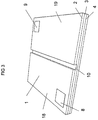
Figure 3 shows an IR detector structure according to a first embodiment of the invention, -
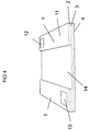
Figure 4 shows an IR detector structure according to a second embodiment of the invention, and -
Figure 5 shows an IR detector structure according to a third embodiment of the invention. -
Figure 1 shows asemiconductor component 1 comprising a first, active,layer 3 comprising one or several electrically conducting layers embedded on both sides by a second layer, acontact layer active layer 3 has an electrical conductivity that is lower than the conductivity in thecontact layers contact layers semiconductor component 1 has greater dimensions in the lateral direction, i.e. in the plane of the layers, than it has in the direction perpendicular to this plane. - In a design according to prior art technology, shown in
Figure 2 , thegroove 7 passes through alllayers lower electrode 6 and theupper electrode 5. The electrical resistance between the twoelectrodes active layer 3, the surface area of the electrodes, and the thickness of the active layer. - According to the invention, the electrodes have an extension in the lateral direction that is less than the lateral dimensions of the semiconductor component. Furthermore, a
groove 10; 14; 17 is present through at least the upper 2 of the contact layers. Furthermore,electrodes - According to one embodiment, the
active layer 3 is a temperature-sensitive layer. - According to a further embodiment, the
active layer 3 is a thermistor layer comprising alternate quantum well layers or quantum dots and barrier layers. - According to a first embodiment of the invention shown in
Figure 3 , thegroove 10 passes through theupper layer 2 of the contact layers. In this way anupper electrode separate electrodes component 1. The electrical current is spread over the complete area of one of the upper contact layers such that it flows down to thelower contact layer 4 and subsequently up to the secondupper contact layer 19. The resistance in this embodiment will be approximately four times higher than it would be according to the embodiment shown inFigure 2 . The resistance, however, still depends on the size of the pixels, i.e. the lateral size of theIR structure 1, which is determined by the optical properties. - The fact is exploited in the present invention that the detector material consists of a multilayer structure in which the electrical conductivity differs significantly between the contact layers 2, 4 and the
active layer 3, and the fact that the lateral dimensions are significantly greater than the vertical dimensions, i.e. the dimensions perpendicular to the plane of the structure. One consequence of this will be that the transport of current through theactive layer 3 will be essentially limited to the volume that lies between thesurrounding contact layers - The freeing of the dependency of the electrical properties and the optical properties has in this way been achieved. Separate optimisation of the optical and the electrical properties becomes in this way possible.
- The lateral dimensions of the structure in
figure 3 may be 30 micrometers. The length of one edge of thesquare electrodes - According to one preferred embodiment, the upper contact layer has a surface area that is less than 10% of the surface area of the semiconductor component.
-
Figure 4 shows a second embodiment of the invention. Thegroove 14 in this embodiment is relatively broad, which leads to the active volume being significantly lower than the volume according to the said second embodiment, with the consequence that the resistance is correspondingly higher. The surface area of the pixel, however, is the same as previously. It is thus possible to optimise the resistance separately from the size of the pixel by adapting the area at theupper contact layer 2. - According to one preferred embodiment, the said
groove 17 is designed such that a lattice of the upper contact layer is formed, which lattice is arranged to increase the optical absorption of incident light that impinges onto the semiconductor component. -
Figure 5 shows this third embodiment of the invention. According to this embodiment, thegroove 17 is so designed that an interlace pattern of theupper contact layer 2 is formed. An optical lattice effect is in this way achieved, in addition to the ability to control the electrical resistance, such that the absorption of incident light increases. - A number of embodiments have been described above. It is, however, obvious that one skilled in the art can vary not only the amount of the upper contact layer that is to be removed, but also its form.
- The present invention is defined by the attached patent claims.
Claims (2)
- A semiconductor bolometer (1) comprising a first, active, layer (3) comprising one or several electrically conducting layers embedded on both sides by a first and a second contact layer (2, 4) respectively, comprising one or several electrically conducting layers, where the active layer (3) has an electrical conductivity that is lower than the conductivity in the contact layers (2, 4), and where an electrode layer is present, connected to a first of the contact layers, and where the semiconductor bolometer (1) has greater dimensions in the lateral direction, i.e. parallel to the plane of the layers, than in the direction perpendicular to said plane, where the electrodes (8, 9; 12, 13; 15, 16) have an extension in the lateral direction that is less than the lateral dimensions of the semiconductor bolometer (1), where a groove (10; 14; 17) is present which passes through said first (2) of the contact layers, and where separate electrodes (8, 9; 12, 13; 15, 16) are present on both sides of the groove (10; 14; 17), characterised in that the active layer (3) is a thermistor layer comprising alternate quantum well layers or quantum dots and barrier layers in that each one of the electrodes (8, 9; 12, 13; 15, 16) on the upper contact layer (2) has a surface area that is less than 10% of the surface area of the semiconductor bolometer (1) and in that the groove is designed such that the magnitude of the surface area of the upper contact layer (2) relative to the magnitude of the upper surface area of the semiconductor bolometer has been adapted to give the semiconductor bolometer (1) a predetermined electrical resistance so that the transport of current through the active layer (3) is essentially limited to the volume that lies between the surrounding contact layers (2,4).
- A semiconductor bolometer according to claim 1, characterised in that the said groove (17) is designed such that a lattice of the upper contact layer (2) is formed, which lattice is arranged to increase the optical absorption of incident light that impinges onto the semiconductor bolometer (1).
Applications Claiming Priority (1)
| Application Number | Priority Date | Filing Date | Title |
|---|---|---|---|
| SE0801497A SE535723C2 (en) | 2008-06-25 | 2008-06-25 | Semiconductor component comprising an active layer surrounded on both sides by a contact layer and with an electrode layer |
Publications (2)
| Publication Number | Publication Date |
|---|---|
| EP2138818A1 EP2138818A1 (en) | 2009-12-30 |
| EP2138818B1 true EP2138818B1 (en) | 2013-11-27 |
Family
ID=40992063
Family Applications (1)
| Application Number | Title | Priority Date | Filing Date |
|---|---|---|---|
| EP09162800.8A Not-in-force EP2138818B1 (en) | 2008-06-25 | 2009-06-16 | Bolometer comprising an active layer surrounded on both sides by a contact layer and with an electrode layer. |
Country Status (2)
| Country | Link |
|---|---|
| EP (1) | EP2138818B1 (en) |
| SE (1) | SE535723C2 (en) |
Families Citing this family (2)
| Publication number | Priority date | Publication date | Assignee | Title |
|---|---|---|---|---|
| MD340Z (en) * | 2010-04-23 | 2011-09-30 | Институт Электронной Инженерии И Промышленных Технологий | Bolometer |
| US11819208B2 (en) | 2021-08-05 | 2023-11-21 | Covidien Lp | Handheld electromechanical surgical device with strain gauge drift detection |
Family Cites Families (1)
| Publication number | Priority date | Publication date | Assignee | Title |
|---|---|---|---|---|
| JP3357247B2 (en) | 1996-08-23 | 2002-12-16 | アルプス電気株式会社 | Temperature sensing element and radiation sensor |
-
2008
- 2008-06-25 SE SE0801497A patent/SE535723C2/en not_active IP Right Cessation
-
2009
- 2009-06-16 EP EP09162800.8A patent/EP2138818B1/en not_active Not-in-force
Non-Patent Citations (1)
| Title |
|---|
| STANLEY WISSMAR ET AL: "High signal-to-noise ratio quantum well bolometer materials", PROCEEDINGS OF SPIE, vol. 6401, 1 January 2006 (2006-01-01), pages 64010N - 64010N-11, XP055013321, ISSN: 0277-786X, DOI: 10.1117/12.689874 * |
Also Published As
| Publication number | Publication date |
|---|---|
| SE535723C2 (en) | 2012-11-27 |
| EP2138818A1 (en) | 2009-12-30 |
| SE0801497L (en) | 2009-12-26 |
Similar Documents
| Publication | Publication Date | Title |
|---|---|---|
| US9269739B2 (en) | Access-resistant diode array device having enhanced stability | |
| US8569857B2 (en) | Diode bolometer and method for producing a diode bolometer | |
| US8759932B2 (en) | Photodetector with a plasmonic structure | |
| US6777681B1 (en) | Infrared detector with amorphous silicon detector elements, and a method of making it | |
| US20110053737A1 (en) | Pressure sensor and boxing machine using the same | |
| US9236415B2 (en) | Diode matrix device with enhanced stability | |
| KR20150090028A (en) | Cmos bolometer | |
| KR20170071415A (en) | Detection device with suspended bolometric membranes having a high absorption efficiency and signal-to-noise ratio | |
| KR100860184B1 (en) | Infrared array detection device | |
| CN113015890A (en) | Infrared sensor and infrared sensor array | |
| US7232998B2 (en) | Bolometer-type infrared solid-state image sensor | |
| US20110266444A1 (en) | Pixel structure for microbolometer detector | |
| EP0873500B1 (en) | Structures for temperature sensors and infrared detectors | |
| EP2942609B1 (en) | Bolometer and method for measurement of electromagnetic radiation | |
| JP3859479B2 (en) | Bolometer type infrared detector | |
| EP2138818A1 (en) | Bolometer comprising an active layer surrounded on both sides by a contact layer and with an electrode layer. | |
| US20160111460A1 (en) | Back-lit photodetector | |
| EP3557203B1 (en) | Light detector | |
| KR20100080604A (en) | Device for detecting heat radiation with high resolution and method for the production thereof | |
| JP5452511B2 (en) | Solid-state imaging device | |
| KR102916191B1 (en) | Microbolometer with reduced pixel pitch | |
| EP3502638A1 (en) | Pyroelectric sensor with electromagnetic shielding comprising a composite material | |
| JP3715886B2 (en) | Manufacturing method and structure of thermal infrared solid-state imaging device | |
| JPH0534610B2 (en) | ||
| KR102916210B1 (en) | Microbolometer with filtering function |
Legal Events
| Date | Code | Title | Description |
|---|---|---|---|
| PUAI | Public reference made under article 153(3) epc to a published international application that has entered the european phase |
Free format text: ORIGINAL CODE: 0009012 |
|
| AK | Designated contracting states |
Kind code of ref document: A1 Designated state(s): AT BE BG CH CY CZ DE DK EE ES FI FR GB GR HR HU IE IS IT LI LT LU LV MC MK MT NL NO PL PT RO SE SI SK TR |
|
| 17P | Request for examination filed |
Effective date: 20100601 |
|
| 17Q | First examination report despatched |
Effective date: 20100624 |
|
| RAP1 | Party data changed (applicant data changed or rights of an application transferred) |
Owner name: ACREO SWEDISH ICT AB |
|
| GRAP | Despatch of communication of intention to grant a patent |
Free format text: ORIGINAL CODE: EPIDOSNIGR1 |
|
| INTG | Intention to grant announced |
Effective date: 20130625 |
|
| GRAS | Grant fee paid |
Free format text: ORIGINAL CODE: EPIDOSNIGR3 |
|
| GRAA | (expected) grant |
Free format text: ORIGINAL CODE: 0009210 |
|
| AK | Designated contracting states |
Kind code of ref document: B1 Designated state(s): AT BE BG CH CY CZ DE DK EE ES FI FR GB GR HR HU IE IS IT LI LT LU LV MC MK MT NL NO PL PT RO SE SI SK TR |
|
| REG | Reference to a national code |
Ref country code: GB Ref legal event code: FG4D |
|
| REG | Reference to a national code |
Ref country code: CH Ref legal event code: EP |
|
| REG | Reference to a national code |
Ref country code: AT Ref legal event code: REF Ref document number: 642902 Country of ref document: AT Kind code of ref document: T Effective date: 20131215 |
|
| REG | Reference to a national code |
Ref country code: IE Ref legal event code: FG4D |
|
| REG | Reference to a national code |
Ref country code: DE Ref legal event code: R096 Ref document number: 602009020367 Country of ref document: DE Effective date: 20140123 |
|
| REG | Reference to a national code |
Ref country code: NL Ref legal event code: VDEP Effective date: 20131127 |
|
| REG | Reference to a national code |
Ref country code: AT Ref legal event code: MK05 Ref document number: 642902 Country of ref document: AT Kind code of ref document: T Effective date: 20131127 |
|
| REG | Reference to a national code |
Ref country code: LT Ref legal event code: MG4D |
|
| PG25 | Lapsed in a contracting state [announced via postgrant information from national office to epo] |
Ref country code: IS Free format text: LAPSE BECAUSE OF FAILURE TO SUBMIT A TRANSLATION OF THE DESCRIPTION OR TO PAY THE FEE WITHIN THE PRESCRIBED TIME-LIMIT Effective date: 20140327 Ref country code: NL Free format text: LAPSE BECAUSE OF FAILURE TO SUBMIT A TRANSLATION OF THE DESCRIPTION OR TO PAY THE FEE WITHIN THE PRESCRIBED TIME-LIMIT Effective date: 20131127 Ref country code: FI Free format text: LAPSE BECAUSE OF FAILURE TO SUBMIT A TRANSLATION OF THE DESCRIPTION OR TO PAY THE FEE WITHIN THE PRESCRIBED TIME-LIMIT Effective date: 20131127 Ref country code: NO Free format text: LAPSE BECAUSE OF FAILURE TO SUBMIT A TRANSLATION OF THE DESCRIPTION OR TO PAY THE FEE WITHIN THE PRESCRIBED TIME-LIMIT Effective date: 20140227 Ref country code: LT Free format text: LAPSE BECAUSE OF FAILURE TO SUBMIT A TRANSLATION OF THE DESCRIPTION OR TO PAY THE FEE WITHIN THE PRESCRIBED TIME-LIMIT Effective date: 20131127 Ref country code: HR Free format text: LAPSE BECAUSE OF FAILURE TO SUBMIT A TRANSLATION OF THE DESCRIPTION OR TO PAY THE FEE WITHIN THE PRESCRIBED TIME-LIMIT Effective date: 20131127 Ref country code: SE Free format text: LAPSE BECAUSE OF FAILURE TO SUBMIT A TRANSLATION OF THE DESCRIPTION OR TO PAY THE FEE WITHIN THE PRESCRIBED TIME-LIMIT Effective date: 20131127 |
|
| PG25 | Lapsed in a contracting state [announced via postgrant information from national office to epo] |
Ref country code: AT Free format text: LAPSE BECAUSE OF FAILURE TO SUBMIT A TRANSLATION OF THE DESCRIPTION OR TO PAY THE FEE WITHIN THE PRESCRIBED TIME-LIMIT Effective date: 20131127 Ref country code: ES Free format text: LAPSE BECAUSE OF FAILURE TO SUBMIT A TRANSLATION OF THE DESCRIPTION OR TO PAY THE FEE WITHIN THE PRESCRIBED TIME-LIMIT Effective date: 20131127 Ref country code: LV Free format text: LAPSE BECAUSE OF FAILURE TO SUBMIT A TRANSLATION OF THE DESCRIPTION OR TO PAY THE FEE WITHIN THE PRESCRIBED TIME-LIMIT Effective date: 20131127 Ref country code: BE Free format text: LAPSE BECAUSE OF FAILURE TO SUBMIT A TRANSLATION OF THE DESCRIPTION OR TO PAY THE FEE WITHIN THE PRESCRIBED TIME-LIMIT Effective date: 20131127 Ref country code: CY Free format text: LAPSE BECAUSE OF FAILURE TO SUBMIT A TRANSLATION OF THE DESCRIPTION OR TO PAY THE FEE WITHIN THE PRESCRIBED TIME-LIMIT Effective date: 20131127 |
|
| PG25 | Lapsed in a contracting state [announced via postgrant information from national office to epo] |
Ref country code: PT Free format text: LAPSE BECAUSE OF FAILURE TO SUBMIT A TRANSLATION OF THE DESCRIPTION OR TO PAY THE FEE WITHIN THE PRESCRIBED TIME-LIMIT Effective date: 20140327 |
|
| PG25 | Lapsed in a contracting state [announced via postgrant information from national office to epo] |
Ref country code: EE Free format text: LAPSE BECAUSE OF FAILURE TO SUBMIT A TRANSLATION OF THE DESCRIPTION OR TO PAY THE FEE WITHIN THE PRESCRIBED TIME-LIMIT Effective date: 20131127 |
|
| REG | Reference to a national code |
Ref country code: DE Ref legal event code: R097 Ref document number: 602009020367 Country of ref document: DE |
|
| PG25 | Lapsed in a contracting state [announced via postgrant information from national office to epo] |
Ref country code: RO Free format text: LAPSE BECAUSE OF FAILURE TO SUBMIT A TRANSLATION OF THE DESCRIPTION OR TO PAY THE FEE WITHIN THE PRESCRIBED TIME-LIMIT Effective date: 20131127 Ref country code: PL Free format text: LAPSE BECAUSE OF FAILURE TO SUBMIT A TRANSLATION OF THE DESCRIPTION OR TO PAY THE FEE WITHIN THE PRESCRIBED TIME-LIMIT Effective date: 20131127 Ref country code: SK Free format text: LAPSE BECAUSE OF FAILURE TO SUBMIT A TRANSLATION OF THE DESCRIPTION OR TO PAY THE FEE WITHIN THE PRESCRIBED TIME-LIMIT Effective date: 20131127 Ref country code: CZ Free format text: LAPSE BECAUSE OF FAILURE TO SUBMIT A TRANSLATION OF THE DESCRIPTION OR TO PAY THE FEE WITHIN THE PRESCRIBED TIME-LIMIT Effective date: 20131127 |
|
| PG25 | Lapsed in a contracting state [announced via postgrant information from national office to epo] |
Ref country code: DK Free format text: LAPSE BECAUSE OF FAILURE TO SUBMIT A TRANSLATION OF THE DESCRIPTION OR TO PAY THE FEE WITHIN THE PRESCRIBED TIME-LIMIT Effective date: 20131127 |
|
| PLBE | No opposition filed within time limit |
Free format text: ORIGINAL CODE: 0009261 |
|
| STAA | Information on the status of an ep patent application or granted ep patent |
Free format text: STATUS: NO OPPOSITION FILED WITHIN TIME LIMIT |
|
| 26N | No opposition filed |
Effective date: 20140828 |
|
| REG | Reference to a national code |
Ref country code: DE Ref legal event code: R097 Ref document number: 602009020367 Country of ref document: DE Effective date: 20140828 |
|
| PG25 | Lapsed in a contracting state [announced via postgrant information from national office to epo] |
Ref country code: LU Free format text: LAPSE BECAUSE OF FAILURE TO SUBMIT A TRANSLATION OF THE DESCRIPTION OR TO PAY THE FEE WITHIN THE PRESCRIBED TIME-LIMIT Effective date: 20140616 Ref country code: MC Free format text: LAPSE BECAUSE OF FAILURE TO SUBMIT A TRANSLATION OF THE DESCRIPTION OR TO PAY THE FEE WITHIN THE PRESCRIBED TIME-LIMIT Effective date: 20131127 |
|
| REG | Reference to a national code |
Ref country code: CH Ref legal event code: PL |
|
| PG25 | Lapsed in a contracting state [announced via postgrant information from national office to epo] |
Ref country code: SI Free format text: LAPSE BECAUSE OF FAILURE TO SUBMIT A TRANSLATION OF THE DESCRIPTION OR TO PAY THE FEE WITHIN THE PRESCRIBED TIME-LIMIT Effective date: 20131127 |
|
| REG | Reference to a national code |
Ref country code: IE Ref legal event code: MM4A |
|
| PG25 | Lapsed in a contracting state [announced via postgrant information from national office to epo] |
Ref country code: LI Free format text: LAPSE BECAUSE OF NON-PAYMENT OF DUE FEES Effective date: 20140630 Ref country code: IT Free format text: LAPSE BECAUSE OF FAILURE TO SUBMIT A TRANSLATION OF THE DESCRIPTION OR TO PAY THE FEE WITHIN THE PRESCRIBED TIME-LIMIT Effective date: 20131127 Ref country code: CH Free format text: LAPSE BECAUSE OF NON-PAYMENT OF DUE FEES Effective date: 20140630 Ref country code: IE Free format text: LAPSE BECAUSE OF NON-PAYMENT OF DUE FEES Effective date: 20140616 |
|
| PG25 | Lapsed in a contracting state [announced via postgrant information from national office to epo] |
Ref country code: MT Free format text: LAPSE BECAUSE OF FAILURE TO SUBMIT A TRANSLATION OF THE DESCRIPTION OR TO PAY THE FEE WITHIN THE PRESCRIBED TIME-LIMIT Effective date: 20131127 |
|
| REG | Reference to a national code |
Ref country code: FR Ref legal event code: PLFP Year of fee payment: 8 |
|
| PG25 | Lapsed in a contracting state [announced via postgrant information from national office to epo] |
Ref country code: BG Free format text: LAPSE BECAUSE OF FAILURE TO SUBMIT A TRANSLATION OF THE DESCRIPTION OR TO PAY THE FEE WITHIN THE PRESCRIBED TIME-LIMIT Effective date: 20131127 Ref country code: GR Free format text: LAPSE BECAUSE OF FAILURE TO SUBMIT A TRANSLATION OF THE DESCRIPTION OR TO PAY THE FEE WITHIN THE PRESCRIBED TIME-LIMIT Effective date: 20140228 |
|
| PG25 | Lapsed in a contracting state [announced via postgrant information from national office to epo] |
Ref country code: HU Free format text: LAPSE BECAUSE OF FAILURE TO SUBMIT A TRANSLATION OF THE DESCRIPTION OR TO PAY THE FEE WITHIN THE PRESCRIBED TIME-LIMIT; INVALID AB INITIO Effective date: 20090616 Ref country code: TR Free format text: LAPSE BECAUSE OF FAILURE TO SUBMIT A TRANSLATION OF THE DESCRIPTION OR TO PAY THE FEE WITHIN THE PRESCRIBED TIME-LIMIT Effective date: 20131127 |
|
| REG | Reference to a national code |
Ref country code: FR Ref legal event code: PLFP Year of fee payment: 9 |
|
| PGFP | Annual fee paid to national office [announced via postgrant information from national office to epo] |
Ref country code: GB Payment date: 20170526 Year of fee payment: 9 Ref country code: FR Payment date: 20170519 Year of fee payment: 9 Ref country code: DE Payment date: 20170519 Year of fee payment: 9 |
|
| PG25 | Lapsed in a contracting state [announced via postgrant information from national office to epo] |
Ref country code: MK Free format text: LAPSE BECAUSE OF FAILURE TO SUBMIT A TRANSLATION OF THE DESCRIPTION OR TO PAY THE FEE WITHIN THE PRESCRIBED TIME-LIMIT Effective date: 20131127 |
|
| REG | Reference to a national code |
Ref country code: DE Ref legal event code: R119 Ref document number: 602009020367 Country of ref document: DE |
|
| GBPC | Gb: european patent ceased through non-payment of renewal fee |
Effective date: 20180616 |
|
| PG25 | Lapsed in a contracting state [announced via postgrant information from national office to epo] |
Ref country code: FR Free format text: LAPSE BECAUSE OF NON-PAYMENT OF DUE FEES Effective date: 20180630 Ref country code: DE Free format text: LAPSE BECAUSE OF NON-PAYMENT OF DUE FEES Effective date: 20190101 Ref country code: GB Free format text: LAPSE BECAUSE OF NON-PAYMENT OF DUE FEES Effective date: 20180616 |