EP2136421B1 - New synthesis of hybrid polymer-metal nanostructures and hybrid polymer-metal compounds nanostructures for nanodevice applications - Google Patents
New synthesis of hybrid polymer-metal nanostructures and hybrid polymer-metal compounds nanostructures for nanodevice applications Download PDFInfo
- Publication number
- EP2136421B1 EP2136421B1 EP08010990.3A EP08010990A EP2136421B1 EP 2136421 B1 EP2136421 B1 EP 2136421B1 EP 08010990 A EP08010990 A EP 08010990A EP 2136421 B1 EP2136421 B1 EP 2136421B1
- Authority
- EP
- European Patent Office
- Prior art keywords
- nanostructures
- metal
- nanoparticles
- hybrid
- hybrid polymer
- Prior art date
- Legal status (The legal status is an assumption and is not a legal conclusion. Google has not performed a legal analysis and makes no representation as to the accuracy of the status listed.)
- Not-in-force
Links
- 239000002086 nanomaterial Substances 0.000 title claims description 117
- 229910052751 metal Inorganic materials 0.000 title claims description 49
- 239000002184 metal Substances 0.000 title claims description 49
- 230000015572 biosynthetic process Effects 0.000 title description 13
- 238000003786 synthesis reaction Methods 0.000 title description 9
- 238000000034 method Methods 0.000 claims description 55
- 239000010931 gold Substances 0.000 claims description 45
- 229910052737 gold Inorganic materials 0.000 claims description 42
- 239000002105 nanoparticle Substances 0.000 claims description 41
- 239000006185 dispersion Substances 0.000 claims description 28
- 239000002082 metal nanoparticle Substances 0.000 claims description 28
- 239000002121 nanofiber Substances 0.000 claims description 24
- 229920000767 polyaniline Polymers 0.000 claims description 23
- PCHJSUWPFVWCPO-UHFFFAOYSA-N gold Chemical compound [Au] PCHJSUWPFVWCPO-UHFFFAOYSA-N 0.000 claims description 19
- YMWUJEATGCHHMB-UHFFFAOYSA-N Dichloromethane Chemical compound ClCCl YMWUJEATGCHHMB-UHFFFAOYSA-N 0.000 claims description 16
- 150000002736 metal compounds Chemical class 0.000 claims description 15
- 239000002322 conducting polymer Substances 0.000 claims description 14
- 229920001940 conductive polymer Polymers 0.000 claims description 14
- 239000008346 aqueous phase Substances 0.000 claims description 10
- YXFVVABEGXRONW-UHFFFAOYSA-N Toluene Chemical compound CC1=CC=CC=C1 YXFVVABEGXRONW-UHFFFAOYSA-N 0.000 claims description 9
- 239000002245 particle Substances 0.000 claims description 9
- 239000013110 organic ligand Substances 0.000 claims description 8
- VZGDMQKNWNREIO-UHFFFAOYSA-N tetrachloromethane Chemical compound ClC(Cl)(Cl)Cl VZGDMQKNWNREIO-UHFFFAOYSA-N 0.000 claims description 8
- 230000000379 polymerizing effect Effects 0.000 claims description 7
- UHOVQNZJYSORNB-UHFFFAOYSA-N Benzene Chemical compound C1=CC=CC=C1 UHOVQNZJYSORNB-UHFFFAOYSA-N 0.000 claims description 6
- HEDRZPFGACZZDS-UHFFFAOYSA-N Chloroform Chemical compound ClC(Cl)Cl HEDRZPFGACZZDS-UHFFFAOYSA-N 0.000 claims description 6
- RTZKZFJDLAIYFH-UHFFFAOYSA-N Diethyl ether Chemical compound CCOCC RTZKZFJDLAIYFH-UHFFFAOYSA-N 0.000 claims description 6
- XEKOWRVHYACXOJ-UHFFFAOYSA-N Ethyl acetate Chemical compound CCOC(C)=O XEKOWRVHYACXOJ-UHFFFAOYSA-N 0.000 claims description 6
- ZMXDDKWLCZADIW-UHFFFAOYSA-N N,N-Dimethylformamide Chemical compound CN(C)C=O ZMXDDKWLCZADIW-UHFFFAOYSA-N 0.000 claims description 6
- 239000000178 monomer Substances 0.000 claims description 6
- VLKZOEOYAKHREP-UHFFFAOYSA-N n-Hexane Chemical compound CCCCCC VLKZOEOYAKHREP-UHFFFAOYSA-N 0.000 claims description 6
- LFQSCWFLJHTTHZ-UHFFFAOYSA-N Ethanol Chemical compound CCO LFQSCWFLJHTTHZ-UHFFFAOYSA-N 0.000 claims description 5
- SECXISVLQFMRJM-UHFFFAOYSA-N N-Methylpyrrolidone Chemical compound CN1CCCC1=O SECXISVLQFMRJM-UHFFFAOYSA-N 0.000 claims description 4
- KDLHZDBZIXYQEI-UHFFFAOYSA-N Palladium Chemical compound [Pd] KDLHZDBZIXYQEI-UHFFFAOYSA-N 0.000 claims description 4
- WYURNTSHIVDZCO-UHFFFAOYSA-N Tetrahydrofuran Chemical compound C1CCOC1 WYURNTSHIVDZCO-UHFFFAOYSA-N 0.000 claims description 4
- 230000002051 biphasic effect Effects 0.000 claims description 4
- BASFCYQUMIYNBI-UHFFFAOYSA-N platinum Chemical compound [Pt] BASFCYQUMIYNBI-UHFFFAOYSA-N 0.000 claims description 4
- 238000012695 Interfacial polymerization Methods 0.000 claims description 3
- RTAQQCXQSZGOHL-UHFFFAOYSA-N Titanium Chemical compound [Ti] RTAQQCXQSZGOHL-UHFFFAOYSA-N 0.000 claims description 3
- 229910052719 titanium Inorganic materials 0.000 claims description 3
- 239000010936 titanium Substances 0.000 claims description 3
- RYGMFSIKBFXOCR-UHFFFAOYSA-N Copper Chemical compound [Cu] RYGMFSIKBFXOCR-UHFFFAOYSA-N 0.000 claims description 2
- FXHOOIRPVKKKFG-UHFFFAOYSA-N N,N-Dimethylacetamide Chemical compound CN(C)C(C)=O FXHOOIRPVKKKFG-UHFFFAOYSA-N 0.000 claims description 2
- CTQNGGLPUBDAKN-UHFFFAOYSA-N O-Xylene Chemical compound CC1=CC=CC=C1C CTQNGGLPUBDAKN-UHFFFAOYSA-N 0.000 claims description 2
- BQCADISMDOOEFD-UHFFFAOYSA-N Silver Chemical compound [Ag] BQCADISMDOOEFD-UHFFFAOYSA-N 0.000 claims description 2
- 239000003153 chemical reaction reagent Substances 0.000 claims description 2
- 229910017052 cobalt Inorganic materials 0.000 claims description 2
- 239000010941 cobalt Substances 0.000 claims description 2
- GUTLYIVDDKVIGB-UHFFFAOYSA-N cobalt atom Chemical compound [Co] GUTLYIVDDKVIGB-UHFFFAOYSA-N 0.000 claims description 2
- 229910052802 copper Inorganic materials 0.000 claims description 2
- 239000010949 copper Substances 0.000 claims description 2
- 229960004132 diethyl ether Drugs 0.000 claims description 2
- 229940113088 dimethylacetamide Drugs 0.000 claims description 2
- JBTWLSYIZRCDFO-UHFFFAOYSA-N ethyl methyl carbonate Chemical compound CCOC(=O)OC JBTWLSYIZRCDFO-UHFFFAOYSA-N 0.000 claims description 2
- 238000002156 mixing Methods 0.000 claims description 2
- 229910052763 palladium Inorganic materials 0.000 claims description 2
- 229910052697 platinum Inorganic materials 0.000 claims description 2
- 239000003880 polar aprotic solvent Substances 0.000 claims description 2
- 229910052709 silver Inorganic materials 0.000 claims description 2
- 239000004332 silver Substances 0.000 claims description 2
- YLQBMQCUIZJEEH-UHFFFAOYSA-N tetrahydrofuran Natural products C=1C=COC=1 YLQBMQCUIZJEEH-UHFFFAOYSA-N 0.000 claims description 2
- 239000008096 xylene Substances 0.000 claims description 2
- QGJOPFRUJISHPQ-NJFSPNSNSA-N carbon disulfide-14c Chemical compound S=[14C]=S QGJOPFRUJISHPQ-NJFSPNSNSA-N 0.000 claims 1
- 150000002148 esters Chemical class 0.000 claims 1
- 229910003472 fullerene Inorganic materials 0.000 description 25
- 239000000463 material Substances 0.000 description 16
- 239000011159 matrix material Substances 0.000 description 15
- 230000008569 process Effects 0.000 description 15
- -1 metals compounds Chemical class 0.000 description 14
- XMWRBQBLMFGWIX-UHFFFAOYSA-N C60 fullerene Chemical class C12=C3C(C4=C56)=C7C8=C5C5=C9C%10=C6C6=C4C1=C1C4=C6C6=C%10C%10=C9C9=C%11C5=C8C5=C8C7=C3C3=C7C2=C1C1=C2C4=C6C4=C%10C6=C9C9=C%11C5=C5C8=C3C3=C7C1=C1C2=C4C6=C2C9=C5C3=C12 XMWRBQBLMFGWIX-UHFFFAOYSA-N 0.000 description 13
- 229920000642 polymer Polymers 0.000 description 13
- 238000006116 polymerization reaction Methods 0.000 description 13
- 239000002131 composite material Substances 0.000 description 9
- 238000004519 manufacturing process Methods 0.000 description 7
- XLYOFNOQVPJJNP-UHFFFAOYSA-N water Substances O XLYOFNOQVPJJNP-UHFFFAOYSA-N 0.000 description 7
- OKTJSMMVPCPJKN-UHFFFAOYSA-N Carbon Chemical compound [C] OKTJSMMVPCPJKN-UHFFFAOYSA-N 0.000 description 6
- 238000009826 distribution Methods 0.000 description 6
- 230000003993 interaction Effects 0.000 description 6
- 239000012074 organic phase Substances 0.000 description 6
- WBIQQQGBSDOWNP-UHFFFAOYSA-N 2-dodecylbenzenesulfonic acid Chemical compound CCCCCCCCCCCCC1=CC=CC=C1S(O)(=O)=O WBIQQQGBSDOWNP-UHFFFAOYSA-N 0.000 description 5
- 239000008367 deionised water Substances 0.000 description 5
- 229910021641 deionized water Inorganic materials 0.000 description 5
- 229940060296 dodecylbenzenesulfonic acid Drugs 0.000 description 5
- 238000002360 preparation method Methods 0.000 description 5
- 239000000126 substance Substances 0.000 description 5
- MIOPJNTWMNEORI-GMSGAONNSA-N (S)-camphorsulfonic acid Chemical compound C1C[C@@]2(CS(O)(=O)=O)C(=O)C[C@@H]1C2(C)C MIOPJNTWMNEORI-GMSGAONNSA-N 0.000 description 4
- CSCPPACGZOOCGX-UHFFFAOYSA-N Acetone Chemical compound CC(C)=O CSCPPACGZOOCGX-UHFFFAOYSA-N 0.000 description 4
- PAYRUJLWNCNPSJ-UHFFFAOYSA-N Aniline Chemical compound NC1=CC=CC=C1 PAYRUJLWNCNPSJ-UHFFFAOYSA-N 0.000 description 4
- 239000004793 Polystyrene Substances 0.000 description 4
- ROOXNKNUYICQNP-UHFFFAOYSA-N ammonium persulfate Chemical compound [NH4+].[NH4+].[O-]S(=O)(=O)OOS([O-])(=O)=O ROOXNKNUYICQNP-UHFFFAOYSA-N 0.000 description 4
- 229910052799 carbon Inorganic materials 0.000 description 4
- 230000015556 catabolic process Effects 0.000 description 4
- 238000012512 characterization method Methods 0.000 description 4
- 238000006243 chemical reaction Methods 0.000 description 4
- 239000003795 chemical substances by application Substances 0.000 description 4
- 238000006731 degradation reaction Methods 0.000 description 4
- WNAHIZMDSQCWRP-UHFFFAOYSA-N dodecane-1-thiol Chemical compound CCCCCCCCCCCCS WNAHIZMDSQCWRP-UHFFFAOYSA-N 0.000 description 4
- 239000002019 doping agent Substances 0.000 description 4
- 239000003999 initiator Substances 0.000 description 4
- 239000002923 metal particle Substances 0.000 description 4
- 150000002739 metals Chemical class 0.000 description 4
- 229920002223 polystyrene Polymers 0.000 description 4
- 239000004094 surface-active agent Substances 0.000 description 4
- 238000002411 thermogravimetry Methods 0.000 description 4
- QTBSBXVTEAMEQO-UHFFFAOYSA-N Acetic acid Chemical compound CC(O)=O QTBSBXVTEAMEQO-UHFFFAOYSA-N 0.000 description 3
- 229920003171 Poly (ethylene oxide) Polymers 0.000 description 3
- 229910052782 aluminium Inorganic materials 0.000 description 3
- XAGFODPZIPBFFR-UHFFFAOYSA-N aluminium Chemical compound [Al] XAGFODPZIPBFFR-UHFFFAOYSA-N 0.000 description 3
- 238000013500 data storage Methods 0.000 description 3
- 238000000354 decomposition reaction Methods 0.000 description 3
- 230000003247 decreasing effect Effects 0.000 description 3
- 238000009792 diffusion process Methods 0.000 description 3
- 238000012377 drug delivery Methods 0.000 description 3
- 230000005669 field effect Effects 0.000 description 3
- 239000011521 glass Substances 0.000 description 3
- 239000000203 mixture Substances 0.000 description 3
- 150000003839 salts Chemical class 0.000 description 3
- 238000000527 sonication Methods 0.000 description 3
- 239000000758 substrate Substances 0.000 description 3
- 238000012360 testing method Methods 0.000 description 3
- LSNNMFCWUKXFEE-UHFFFAOYSA-M Bisulfite Chemical compound OS([O-])=O LSNNMFCWUKXFEE-UHFFFAOYSA-M 0.000 description 2
- MHAJPDPJQMAIIY-UHFFFAOYSA-N Hydrogen peroxide Chemical compound OO MHAJPDPJQMAIIY-UHFFFAOYSA-N 0.000 description 2
- XEEYBQQBJWHFJM-UHFFFAOYSA-N Iron Chemical compound [Fe] XEEYBQQBJWHFJM-UHFFFAOYSA-N 0.000 description 2
- AFVFQIVMOAPDHO-UHFFFAOYSA-N Methanesulfonic acid Chemical compound CS(O)(=O)=O AFVFQIVMOAPDHO-UHFFFAOYSA-N 0.000 description 2
- OJGMBLNIHDZDGS-UHFFFAOYSA-N N-Ethylaniline Chemical compound CCNC1=CC=CC=C1 OJGMBLNIHDZDGS-UHFFFAOYSA-N 0.000 description 2
- PXHVJJICTQNCMI-UHFFFAOYSA-N Nickel Chemical compound [Ni] PXHVJJICTQNCMI-UHFFFAOYSA-N 0.000 description 2
- KAESVJOAVNADME-UHFFFAOYSA-N Pyrrole Chemical compound C=1C=CNC=1 KAESVJOAVNADME-UHFFFAOYSA-N 0.000 description 2
- FOIXSVOLVBLSDH-UHFFFAOYSA-N Silver ion Chemical compound [Ag+] FOIXSVOLVBLSDH-UHFFFAOYSA-N 0.000 description 2
- YTPLMLYBLZKORZ-UHFFFAOYSA-N Thiophene Chemical compound C=1C=CSC=1 YTPLMLYBLZKORZ-UHFFFAOYSA-N 0.000 description 2
- 239000002253 acid Substances 0.000 description 2
- 125000000217 alkyl group Chemical group 0.000 description 2
- 229910001870 ammonium persulfate Inorganic materials 0.000 description 2
- 229910052980 cadmium sulfide Inorganic materials 0.000 description 2
- MIOPJNTWMNEORI-UHFFFAOYSA-N camphorsulfonic acid Chemical compound C1CC2(CS(O)(=O)=O)C(=O)CC1C2(C)C MIOPJNTWMNEORI-UHFFFAOYSA-N 0.000 description 2
- 239000002041 carbon nanotube Substances 0.000 description 2
- 229910021393 carbon nanotube Inorganic materials 0.000 description 2
- 238000006555 catalytic reaction Methods 0.000 description 2
- 239000011248 coating agent Substances 0.000 description 2
- 238000000576 coating method Methods 0.000 description 2
- UBEWDCMIDFGDOO-UHFFFAOYSA-N cobalt(2+);cobalt(3+);oxygen(2-) Chemical compound [O-2].[O-2].[O-2].[O-2].[Co+2].[Co+3].[Co+3] UBEWDCMIDFGDOO-UHFFFAOYSA-N 0.000 description 2
- 230000000875 corresponding effect Effects 0.000 description 2
- 239000000539 dimer Substances 0.000 description 2
- 230000002349 favourable effect Effects 0.000 description 2
- 238000001914 filtration Methods 0.000 description 2
- KWIUHFFTVRNATP-UHFFFAOYSA-N glycine betaine Chemical compound C[N+](C)(C)CC([O-])=O KWIUHFFTVRNATP-UHFFFAOYSA-N 0.000 description 2
- BXWNKGSJHAJOGX-UHFFFAOYSA-N hexadecan-1-ol Chemical compound CCCCCCCCCCCCCCCCO BXWNKGSJHAJOGX-UHFFFAOYSA-N 0.000 description 2
- 238000011835 investigation Methods 0.000 description 2
- 238000005259 measurement Methods 0.000 description 2
- 239000007769 metal material Substances 0.000 description 2
- BDAGIHXWWSANSR-UHFFFAOYSA-N methanoic acid Natural products OC=O BDAGIHXWWSANSR-UHFFFAOYSA-N 0.000 description 2
- 230000001590 oxidative effect Effects 0.000 description 2
- 230000000704 physical effect Effects 0.000 description 2
- 229920000728 polyester Polymers 0.000 description 2
- 239000002861 polymer material Substances 0.000 description 2
- 229920002635 polyurethane Polymers 0.000 description 2
- 239000004814 polyurethane Substances 0.000 description 2
- 239000002243 precursor Substances 0.000 description 2
- 238000004528 spin coating Methods 0.000 description 2
- 230000002194 synthesizing effect Effects 0.000 description 2
- CWERGRDVMFNCDR-UHFFFAOYSA-N thioglycolic acid Chemical compound OC(=O)CS CWERGRDVMFNCDR-UHFFFAOYSA-N 0.000 description 2
- NBOMNTLFRHMDEZ-UHFFFAOYSA-N thiosalicylic acid Chemical compound OC(=O)C1=CC=CC=C1S NBOMNTLFRHMDEZ-UHFFFAOYSA-N 0.000 description 2
- WFKWXMTUELFFGS-UHFFFAOYSA-N tungsten Chemical compound [W] WFKWXMTUELFFGS-UHFFFAOYSA-N 0.000 description 2
- 229910052721 tungsten Inorganic materials 0.000 description 2
- 239000010937 tungsten Substances 0.000 description 2
- 229910052984 zinc sulfide Inorganic materials 0.000 description 2
- ALSTYHKOOCGGFT-KTKRTIGZSA-N (9Z)-octadecen-1-ol Chemical compound CCCCCCCC\C=C/CCCCCCCCO ALSTYHKOOCGGFT-KTKRTIGZSA-N 0.000 description 1
- AKIZPWSPNKVOMT-UHFFFAOYSA-N 1-sulfanylhexan-1-ol Chemical compound CCCCCC(O)S AKIZPWSPNKVOMT-UHFFFAOYSA-N 0.000 description 1
- LBLYYCQCTBFVLH-UHFFFAOYSA-N 2-Methylbenzenesulfonic acid Chemical compound CC1=CC=CC=C1S(O)(=O)=O LBLYYCQCTBFVLH-UHFFFAOYSA-N 0.000 description 1
- VRVRGVPWCUEOGV-UHFFFAOYSA-N 2-aminothiophenol Chemical compound NC1=CC=CC=C1S VRVRGVPWCUEOGV-UHFFFAOYSA-N 0.000 description 1
- DYAOREPNYXXCOA-UHFFFAOYSA-N 2-sulfanylundecanoic acid Chemical compound CCCCCCCCCC(S)C(O)=O DYAOREPNYXXCOA-UHFFFAOYSA-N 0.000 description 1
- WUPHOULIZUERAE-UHFFFAOYSA-N 3-(oxolan-2-yl)propanoic acid Chemical compound OC(=O)CCC1CCCO1 WUPHOULIZUERAE-UHFFFAOYSA-N 0.000 description 1
- DKIDEFUBRARXTE-UHFFFAOYSA-N 3-mercaptopropanoic acid Chemical compound OC(=O)CCS DKIDEFUBRARXTE-UHFFFAOYSA-N 0.000 description 1
- OSWFIVFLDKOXQC-UHFFFAOYSA-N 4-(3-methoxyphenyl)aniline Chemical compound COC1=CC=CC(C=2C=CC(N)=CC=2)=C1 OSWFIVFLDKOXQC-UHFFFAOYSA-N 0.000 description 1
- JLBJTVDPSNHSKJ-UHFFFAOYSA-N 4-Methylstyrene Chemical compound CC1=CC=C(C=C)C=C1 JLBJTVDPSNHSKJ-UHFFFAOYSA-N 0.000 description 1
- 229920001817 Agar Polymers 0.000 description 1
- DHMQDGOQFOQNFH-UHFFFAOYSA-M Aminoacetate Chemical compound NCC([O-])=O DHMQDGOQFOQNFH-UHFFFAOYSA-M 0.000 description 1
- QGZKDVFQNNGYKY-UHFFFAOYSA-O Ammonium Chemical compound [NH4+] QGZKDVFQNNGYKY-UHFFFAOYSA-O 0.000 description 1
- 101710158075 Bucky ball Proteins 0.000 description 1
- 229910004613 CdTe Inorganic materials 0.000 description 1
- 229910052684 Cerium Inorganic materials 0.000 description 1
- LZZYPRNAOMGNLH-UHFFFAOYSA-M Cetrimonium bromide Chemical compound [Br-].CCCCCCCCCCCCCCCC[N+](C)(C)C LZZYPRNAOMGNLH-UHFFFAOYSA-M 0.000 description 1
- VYZAMTAEIAYCRO-UHFFFAOYSA-N Chromium Chemical compound [Cr] VYZAMTAEIAYCRO-UHFFFAOYSA-N 0.000 description 1
- 229910002531 CuTe Inorganic materials 0.000 description 1
- FEWJPZIEWOKRBE-JCYAYHJZSA-N Dextrotartaric acid Chemical compound OC(=O)[C@H](O)[C@@H](O)C(O)=O FEWJPZIEWOKRBE-JCYAYHJZSA-N 0.000 description 1
- SNRUBQQJIBEYMU-UHFFFAOYSA-N Dodecane Natural products CCCCCCCCCCCC SNRUBQQJIBEYMU-UHFFFAOYSA-N 0.000 description 1
- 229910052692 Dysprosium Inorganic materials 0.000 description 1
- 229910002601 GaN Inorganic materials 0.000 description 1
- 229910052688 Gadolinium Inorganic materials 0.000 description 1
- 229910052689 Holmium Inorganic materials 0.000 description 1
- VEXZGXHMUGYJMC-UHFFFAOYSA-N Hydrochloric acid Chemical compound Cl VEXZGXHMUGYJMC-UHFFFAOYSA-N 0.000 description 1
- DGAQECJNVWCQMB-PUAWFVPOSA-M Ilexoside XXIX Chemical compound C[C@@H]1CC[C@@]2(CC[C@@]3(C(=CC[C@H]4[C@]3(CC[C@@H]5[C@@]4(CC[C@@H](C5(C)C)OS(=O)(=O)[O-])C)C)[C@@H]2[C@]1(C)O)C)C(=O)O[C@H]6[C@@H]([C@H]([C@@H]([C@H](O6)CO)O)O)O.[Na+] DGAQECJNVWCQMB-PUAWFVPOSA-M 0.000 description 1
- 229910021578 Iron(III) chloride Inorganic materials 0.000 description 1
- 229910002567 K2S2O8 Inorganic materials 0.000 description 1
- 229910052765 Lutetium Inorganic materials 0.000 description 1
- FYYHWMGAXLPEAU-UHFFFAOYSA-N Magnesium Chemical compound [Mg] FYYHWMGAXLPEAU-UHFFFAOYSA-N 0.000 description 1
- ZOKXTWBITQBERF-UHFFFAOYSA-N Molybdenum Chemical compound [Mo] ZOKXTWBITQBERF-UHFFFAOYSA-N 0.000 description 1
- AFBPFSWMIHJQDM-UHFFFAOYSA-N N-methylaniline Chemical compound CNC1=CC=CC=C1 AFBPFSWMIHJQDM-UHFFFAOYSA-N 0.000 description 1
- 229910004882 Na2S2O8 Inorganic materials 0.000 description 1
- 229910019501 NaVO3 Inorganic materials 0.000 description 1
- 229910052779 Neodymium Inorganic materials 0.000 description 1
- GRYLNZFGIOXLOG-UHFFFAOYSA-N Nitric acid Chemical compound O[N+]([O-])=O GRYLNZFGIOXLOG-UHFFFAOYSA-N 0.000 description 1
- 208000012868 Overgrowth Diseases 0.000 description 1
- 229910019142 PO4 Inorganic materials 0.000 description 1
- NBIIXXVUZAFLBC-UHFFFAOYSA-N Phosphoric acid Chemical compound OP(O)(O)=O NBIIXXVUZAFLBC-UHFFFAOYSA-N 0.000 description 1
- 229920001665 Poly-4-vinylphenol Polymers 0.000 description 1
- 239000004952 Polyamide Substances 0.000 description 1
- 239000004642 Polyimide Substances 0.000 description 1
- 239000004372 Polyvinyl alcohol Substances 0.000 description 1
- 229910052777 Praseodymium Inorganic materials 0.000 description 1
- KJTLSVCANCCWHF-UHFFFAOYSA-N Ruthenium Chemical compound [Ru] KJTLSVCANCCWHF-UHFFFAOYSA-N 0.000 description 1
- BUGBHKTXTAQXES-UHFFFAOYSA-N Selenium Chemical compound [Se] BUGBHKTXTAQXES-UHFFFAOYSA-N 0.000 description 1
- QAOWNCQODCNURD-UHFFFAOYSA-N Sulfuric acid Chemical compound OS(O)(=O)=O QAOWNCQODCNURD-UHFFFAOYSA-N 0.000 description 1
- 238000003917 TEM image Methods 0.000 description 1
- 229910052771 Terbium Inorganic materials 0.000 description 1
- ATJFFYVFTNAWJD-UHFFFAOYSA-N Tin Chemical compound [Sn] ATJFFYVFTNAWJD-UHFFFAOYSA-N 0.000 description 1
- GWEVSGVZZGPLCZ-UHFFFAOYSA-N Titan oxide Chemical compound O=[Ti]=O GWEVSGVZZGPLCZ-UHFFFAOYSA-N 0.000 description 1
- HCHKCACWOHOZIP-UHFFFAOYSA-N Zinc Chemical compound [Zn] HCHKCACWOHOZIP-UHFFFAOYSA-N 0.000 description 1
- 239000005083 Zinc sulfide Substances 0.000 description 1
- QCWXUUIWCKQGHC-UHFFFAOYSA-N Zirconium Chemical compound [Zr] QCWXUUIWCKQGHC-UHFFFAOYSA-N 0.000 description 1
- MIOPJNTWMNEORI-OMNKOJBGSA-N [(4s)-7,7-dimethyl-3-oxo-4-bicyclo[2.2.1]heptanyl]methanesulfonic acid Chemical compound C1C[C@@]2(CS(O)(=O)=O)C(=O)CC1C2(C)C MIOPJNTWMNEORI-OMNKOJBGSA-N 0.000 description 1
- DDIPQFCIYCYYHG-UHFFFAOYSA-N [Er].[Ir] Chemical compound [Er].[Ir] DDIPQFCIYCYYHG-UHFFFAOYSA-N 0.000 description 1
- 229910052946 acanthite Inorganic materials 0.000 description 1
- 239000008272 agar Substances 0.000 description 1
- 238000004220 aggregation Methods 0.000 description 1
- 230000002776 aggregation Effects 0.000 description 1
- 150000001298 alcohols Chemical class 0.000 description 1
- 229910045601 alloy Inorganic materials 0.000 description 1
- 239000000956 alloy Substances 0.000 description 1
- 150000001412 amines Chemical class 0.000 description 1
- BTBJBAZGXNKLQC-UHFFFAOYSA-N ammonium lauryl sulfate Chemical compound [NH4+].CCCCCCCCCCCCOS([O-])(=O)=O BTBJBAZGXNKLQC-UHFFFAOYSA-N 0.000 description 1
- 229940063953 ammonium lauryl sulfate Drugs 0.000 description 1
- 238000004458 analytical method Methods 0.000 description 1
- 229910052787 antimony Inorganic materials 0.000 description 1
- WATWJIUSRGPENY-UHFFFAOYSA-N antimony atom Chemical compound [Sb] WATWJIUSRGPENY-UHFFFAOYSA-N 0.000 description 1
- 229960000686 benzalkonium chloride Drugs 0.000 description 1
- 229940077388 benzenesulfonate Drugs 0.000 description 1
- SRSXLGNVWSONIS-UHFFFAOYSA-M benzenesulfonate Chemical compound [O-]S(=O)(=O)C1=CC=CC=C1 SRSXLGNVWSONIS-UHFFFAOYSA-M 0.000 description 1
- 229960001950 benzethonium chloride Drugs 0.000 description 1
- UREZNYTWGJKWBI-UHFFFAOYSA-M benzethonium chloride Chemical compound [Cl-].C1=CC(C(C)(C)CC(C)(C)C)=CC=C1OCCOCC[N+](C)(C)CC1=CC=CC=C1 UREZNYTWGJKWBI-UHFFFAOYSA-M 0.000 description 1
- UENWRTRMUIOCKN-UHFFFAOYSA-N benzyl thiol Chemical compound SCC1=CC=CC=C1 UENWRTRMUIOCKN-UHFFFAOYSA-N 0.000 description 1
- CADWTSSKOVRVJC-UHFFFAOYSA-N benzyl(dimethyl)azanium;chloride Chemical compound [Cl-].C[NH+](C)CC1=CC=CC=C1 CADWTSSKOVRVJC-UHFFFAOYSA-N 0.000 description 1
- 229960003237 betaine Drugs 0.000 description 1
- 229910052797 bismuth Inorganic materials 0.000 description 1
- JCXGWMGPZLAOME-UHFFFAOYSA-N bismuth atom Chemical compound [Bi] JCXGWMGPZLAOME-UHFFFAOYSA-N 0.000 description 1
- 229910052793 cadmium Inorganic materials 0.000 description 1
- BDOSMKKIYDKNTQ-UHFFFAOYSA-N cadmium atom Chemical compound [Cd] BDOSMKKIYDKNTQ-UHFFFAOYSA-N 0.000 description 1
- UHYPYGJEEGLRJD-UHFFFAOYSA-N cadmium(2+);selenium(2-) Chemical compound [Se-2].[Cd+2] UHYPYGJEEGLRJD-UHFFFAOYSA-N 0.000 description 1
- 229910021387 carbon allotrope Inorganic materials 0.000 description 1
- HDFRDWFLWVCOGP-UHFFFAOYSA-N carbonothioic O,S-acid Chemical class OC(S)=O HDFRDWFLWVCOGP-UHFFFAOYSA-N 0.000 description 1
- 239000003054 catalyst Substances 0.000 description 1
- 230000003197 catalytic effect Effects 0.000 description 1
- ZMIGMASIKSOYAM-UHFFFAOYSA-N cerium Chemical compound [Ce][Ce][Ce][Ce][Ce][Ce][Ce][Ce][Ce][Ce][Ce][Ce][Ce][Ce][Ce][Ce][Ce][Ce][Ce][Ce][Ce][Ce][Ce][Ce][Ce][Ce][Ce][Ce][Ce][Ce][Ce][Ce][Ce][Ce][Ce][Ce][Ce][Ce] ZMIGMASIKSOYAM-UHFFFAOYSA-N 0.000 description 1
- 229910000355 cerium(IV) sulfate Inorganic materials 0.000 description 1
- 229960000541 cetyl alcohol Drugs 0.000 description 1
- 229960001927 cetylpyridinium chloride Drugs 0.000 description 1
- YMKDRGPMQRFJGP-UHFFFAOYSA-M cetylpyridinium chloride Chemical compound [Cl-].CCCCCCCCCCCCCCCC[N+]1=CC=CC=C1 YMKDRGPMQRFJGP-UHFFFAOYSA-M 0.000 description 1
- 229910052804 chromium Inorganic materials 0.000 description 1
- 239000011651 chromium Substances 0.000 description 1
- 230000001276 controlling effect Effects 0.000 description 1
- 229920001577 copolymer Polymers 0.000 description 1
- 230000002596 correlated effect Effects 0.000 description 1
- 229960001270 d- tartaric acid Drugs 0.000 description 1
- WOQQAWHSKSSAGF-WXFJLFHKSA-N decyl beta-D-maltopyranoside Chemical compound O[C@@H]1[C@@H](O)[C@H](OCCCCCCCCCC)O[C@H](CO)[C@H]1O[C@@H]1[C@H](O)[C@@H](O)[C@H](O)[C@@H](CO)O1 WOQQAWHSKSSAGF-WXFJLFHKSA-N 0.000 description 1
- 230000001419 dependent effect Effects 0.000 description 1
- 230000006866 deterioration Effects 0.000 description 1
- 238000011161 development Methods 0.000 description 1
- 125000003438 dodecyl group Chemical group [H]C([H])([H])C([H])([H])C([H])([H])C([H])([H])C([H])([H])C([H])([H])C([H])([H])C([H])([H])C([H])([H])C([H])([H])C([H])([H])C([H])([H])* 0.000 description 1
- JRBPAEWTRLWTQC-UHFFFAOYSA-N dodecylamine Chemical compound CCCCCCCCCCCCN JRBPAEWTRLWTQC-UHFFFAOYSA-N 0.000 description 1
- 238000001548 drop coating Methods 0.000 description 1
- KBQHZAAAGSGFKK-UHFFFAOYSA-N dysprosium atom Chemical compound [Dy] KBQHZAAAGSGFKK-UHFFFAOYSA-N 0.000 description 1
- 238000005516 engineering process Methods 0.000 description 1
- 230000007613 environmental effect Effects 0.000 description 1
- CCIVGXIOQKPBKL-UHFFFAOYSA-N ethanesulfonic acid Chemical compound CCS(O)(=O)=O CCIVGXIOQKPBKL-UHFFFAOYSA-N 0.000 description 1
- DNJIEGIFACGWOD-UHFFFAOYSA-N ethyl mercaptane Natural products CCS DNJIEGIFACGWOD-UHFFFAOYSA-N 0.000 description 1
- 238000001704 evaporation Methods 0.000 description 1
- 230000008020 evaporation Effects 0.000 description 1
- 239000000835 fiber Substances 0.000 description 1
- 239000012467 final product Substances 0.000 description 1
- 235000019253 formic acid Nutrition 0.000 description 1
- UIWYJDYFSGRHKR-UHFFFAOYSA-N gadolinium atom Chemical compound [Gd] UIWYJDYFSGRHKR-UHFFFAOYSA-N 0.000 description 1
- 239000007789 gas Substances 0.000 description 1
- 229910052732 germanium Inorganic materials 0.000 description 1
- GNPVGFCGXDBREM-UHFFFAOYSA-N germanium atom Chemical compound [Ge] GNPVGFCGXDBREM-UHFFFAOYSA-N 0.000 description 1
- 229910052735 hafnium Inorganic materials 0.000 description 1
- VBJZVLUMGGDVMO-UHFFFAOYSA-N hafnium atom Chemical compound [Hf] VBJZVLUMGGDVMO-UHFFFAOYSA-N 0.000 description 1
- 238000010438 heat treatment Methods 0.000 description 1
- KJZYNXUDTRRSPN-UHFFFAOYSA-N holmium atom Chemical compound [Ho] KJZYNXUDTRRSPN-UHFFFAOYSA-N 0.000 description 1
- 229920000587 hyperbranched polymer Polymers 0.000 description 1
- 229910052738 indium Inorganic materials 0.000 description 1
- APFVFJFRJDLVQX-UHFFFAOYSA-N indium atom Chemical compound [In] APFVFJFRJDLVQX-UHFFFAOYSA-N 0.000 description 1
- 229910052742 iron Inorganic materials 0.000 description 1
- FBAFATDZDUQKNH-UHFFFAOYSA-M iron chloride Chemical compound [Cl-].[Fe] FBAFATDZDUQKNH-UHFFFAOYSA-M 0.000 description 1
- UQSXHKLRYXJYBZ-UHFFFAOYSA-N iron oxide Inorganic materials [Fe]=O UQSXHKLRYXJYBZ-UHFFFAOYSA-N 0.000 description 1
- 235000013980 iron oxide Nutrition 0.000 description 1
- RBTARNINKXHZNM-UHFFFAOYSA-K iron trichloride Chemical compound Cl[Fe](Cl)Cl RBTARNINKXHZNM-UHFFFAOYSA-K 0.000 description 1
- VBMVTYDPPZVILR-UHFFFAOYSA-N iron(2+);oxygen(2-) Chemical class [O-2].[Fe+2] VBMVTYDPPZVILR-UHFFFAOYSA-N 0.000 description 1
- 150000002576 ketones Chemical class 0.000 description 1
- 229910052746 lanthanum Inorganic materials 0.000 description 1
- FZLIPJUXYLNCLC-UHFFFAOYSA-N lanthanum atom Chemical compound [La] FZLIPJUXYLNCLC-UHFFFAOYSA-N 0.000 description 1
- 239000011133 lead Substances 0.000 description 1
- 229910052981 lead sulfide Inorganic materials 0.000 description 1
- 229940056932 lead sulfide Drugs 0.000 description 1
- FEWJPZIEWOKRBE-LWMBPPNESA-N levotartaric acid Chemical compound OC(=O)[C@@H](O)[C@H](O)C(O)=O FEWJPZIEWOKRBE-LWMBPPNESA-N 0.000 description 1
- OHSVLFRHMCKCQY-UHFFFAOYSA-N lutetium atom Chemical compound [Lu] OHSVLFRHMCKCQY-UHFFFAOYSA-N 0.000 description 1
- 229910052749 magnesium Inorganic materials 0.000 description 1
- 239000011777 magnesium Substances 0.000 description 1
- WPBNNNQJVZRUHP-UHFFFAOYSA-L manganese(2+);methyl n-[[2-(methoxycarbonylcarbamothioylamino)phenyl]carbamothioyl]carbamate;n-[2-(sulfidocarbothioylamino)ethyl]carbamodithioate Chemical compound [Mn+2].[S-]C(=S)NCCNC([S-])=S.COC(=O)NC(=S)NC1=CC=CC=C1NC(=S)NC(=O)OC WPBNNNQJVZRUHP-UHFFFAOYSA-L 0.000 description 1
- 230000000873 masking effect Effects 0.000 description 1
- 230000007246 mechanism Effects 0.000 description 1
- 239000012528 membrane Substances 0.000 description 1
- 125000005358 mercaptoalkyl group Chemical group 0.000 description 1
- 229910021645 metal ion Inorganic materials 0.000 description 1
- 150000001455 metallic ions Chemical class 0.000 description 1
- 239000013528 metallic particle Substances 0.000 description 1
- 229940098779 methanesulfonic acid Drugs 0.000 description 1
- 150000002751 molybdenum Chemical class 0.000 description 1
- 229910052750 molybdenum Inorganic materials 0.000 description 1
- 239000011733 molybdenum Substances 0.000 description 1
- PJUIMOJAAPLTRJ-UHFFFAOYSA-N monothioglycerol Chemical compound OCC(O)CS PJUIMOJAAPLTRJ-UHFFFAOYSA-N 0.000 description 1
- DVEKCXOJTLDBFE-UHFFFAOYSA-N n-dodecyl-n,n-dimethylglycinate Chemical compound CCCCCCCCCCCC[N+](C)(C)CC([O-])=O DVEKCXOJTLDBFE-UHFFFAOYSA-N 0.000 description 1
- 239000002073 nanorod Substances 0.000 description 1
- 239000002135 nanosheet Substances 0.000 description 1
- 239000002071 nanotube Substances 0.000 description 1
- 239000002070 nanowire Substances 0.000 description 1
- PSZYNBSKGUBXEH-UHFFFAOYSA-N naphthalene-1-sulfonic acid Chemical compound C1=CC=C2C(S(=O)(=O)O)=CC=CC2=C1 PSZYNBSKGUBXEH-UHFFFAOYSA-N 0.000 description 1
- QEFYFXOXNSNQGX-UHFFFAOYSA-N neodymium atom Chemical compound [Nd] QEFYFXOXNSNQGX-UHFFFAOYSA-N 0.000 description 1
- 229910052759 nickel Inorganic materials 0.000 description 1
- 229910017604 nitric acid Inorganic materials 0.000 description 1
- 239000012299 nitrogen atmosphere Substances 0.000 description 1
- HEGSGKPQLMEBJL-RKQHYHRCSA-N octyl beta-D-glucopyranoside Chemical compound CCCCCCCCO[C@@H]1O[C@H](CO)[C@@H](O)[C@H](O)[C@H]1O HEGSGKPQLMEBJL-RKQHYHRCSA-N 0.000 description 1
- 229940055577 oleyl alcohol Drugs 0.000 description 1
- XMLQWXUVTXCDDL-UHFFFAOYSA-N oleyl alcohol Natural products CCCCCCC=CCCCCCCCCCCO XMLQWXUVTXCDDL-UHFFFAOYSA-N 0.000 description 1
- 230000003287 optical effect Effects 0.000 description 1
- 229910052762 osmium Inorganic materials 0.000 description 1
- SYQBFIAQOQZEGI-UHFFFAOYSA-N osmium atom Chemical compound [Os] SYQBFIAQOQZEGI-UHFFFAOYSA-N 0.000 description 1
- 239000007800 oxidant agent Substances 0.000 description 1
- RVTZCBVAJQQJTK-UHFFFAOYSA-N oxygen(2-);zirconium(4+) Chemical compound [O-2].[O-2].[Zr+4] RVTZCBVAJQQJTK-UHFFFAOYSA-N 0.000 description 1
- BHAAPTBBJKJZER-UHFFFAOYSA-N p-anisidine Chemical compound COC1=CC=C(N)C=C1 BHAAPTBBJKJZER-UHFFFAOYSA-N 0.000 description 1
- GPNDARIEYHPYAY-UHFFFAOYSA-N palladium(ii) nitrate Chemical compound [Pd+2].[O-][N+]([O-])=O.[O-][N+]([O-])=O GPNDARIEYHPYAY-UHFFFAOYSA-N 0.000 description 1
- VLTRZXGMWDSKGL-UHFFFAOYSA-N perchloric acid Chemical compound OCl(=O)(=O)=O VLTRZXGMWDSKGL-UHFFFAOYSA-N 0.000 description 1
- 239000012071 phase Substances 0.000 description 1
- 239000010452 phosphate Substances 0.000 description 1
- 238000000206 photolithography Methods 0.000 description 1
- 229920002493 poly(chlorotrifluoroethylene) Polymers 0.000 description 1
- 229920001467 poly(styrenesulfonates) Polymers 0.000 description 1
- 229920000172 poly(styrenesulfonic acid) Polymers 0.000 description 1
- 229920002647 polyamide Polymers 0.000 description 1
- 239000005023 polychlorotrifluoroethylene (PCTFE) polymer Substances 0.000 description 1
- 229920002098 polyfluorene Polymers 0.000 description 1
- 229920001721 polyimide Polymers 0.000 description 1
- 239000004926 polymethyl methacrylate Substances 0.000 description 1
- 229920000098 polyolefin Polymers 0.000 description 1
- 229920001184 polypeptide Polymers 0.000 description 1
- 229920001451 polypropylene glycol Polymers 0.000 description 1
- 229920000128 polypyrrole Polymers 0.000 description 1
- 229920001296 polysiloxane Polymers 0.000 description 1
- 229940005642 polystyrene sulfonic acid Drugs 0.000 description 1
- 229920000123 polythiophene Polymers 0.000 description 1
- 229920002451 polyvinyl alcohol Polymers 0.000 description 1
- 239000004800 polyvinyl chloride Substances 0.000 description 1
- 229920000915 polyvinyl chloride Polymers 0.000 description 1
- 229920006316 polyvinylpyrrolidine Polymers 0.000 description 1
- 239000011148 porous material Substances 0.000 description 1
- KMUONIBRACKNSN-UHFFFAOYSA-N potassium dichromate Chemical compound [K+].[K+].[O-][Cr](=O)(=O)O[Cr]([O-])(=O)=O KMUONIBRACKNSN-UHFFFAOYSA-N 0.000 description 1
- 239000012286 potassium permanganate Substances 0.000 description 1
- PUDIUYLPXJFUGB-UHFFFAOYSA-N praseodymium atom Chemical compound [Pr] PUDIUYLPXJFUGB-UHFFFAOYSA-N 0.000 description 1
- 102000004196 processed proteins & peptides Human genes 0.000 description 1
- 108090000765 processed proteins & peptides Proteins 0.000 description 1
- 239000000047 product Substances 0.000 description 1
- 239000011541 reaction mixture Substances 0.000 description 1
- 230000035484 reaction time Effects 0.000 description 1
- 238000006479 redox reaction Methods 0.000 description 1
- 230000001105 regulatory effect Effects 0.000 description 1
- 238000011160 research Methods 0.000 description 1
- 229910052703 rhodium Inorganic materials 0.000 description 1
- 239000010948 rhodium Substances 0.000 description 1
- MHOVAHRLVXNVSD-UHFFFAOYSA-N rhodium atom Chemical compound [Rh] MHOVAHRLVXNVSD-UHFFFAOYSA-N 0.000 description 1
- 229910052707 ruthenium Inorganic materials 0.000 description 1
- 239000000523 sample Substances 0.000 description 1
- 238000005204 segregation Methods 0.000 description 1
- 229910052711 selenium Inorganic materials 0.000 description 1
- 239000011669 selenium Substances 0.000 description 1
- FSJWWSXPIWGYKC-UHFFFAOYSA-M silver;silver;sulfanide Chemical compound [SH-].[Ag].[Ag+] FSJWWSXPIWGYKC-UHFFFAOYSA-M 0.000 description 1
- 239000011734 sodium Substances 0.000 description 1
- 229910052708 sodium Inorganic materials 0.000 description 1
- 239000012279 sodium borohydride Substances 0.000 description 1
- 229910000033 sodium borohydride Inorganic materials 0.000 description 1
- SUKJFIGYRHOWBL-UHFFFAOYSA-N sodium hypochlorite Chemical compound [Na+].Cl[O-] SUKJFIGYRHOWBL-UHFFFAOYSA-N 0.000 description 1
- 229940057950 sodium laureth sulfate Drugs 0.000 description 1
- CMZUMMUJMWNLFH-UHFFFAOYSA-N sodium metavanadate Chemical compound [Na+].[O-][V](=O)=O CMZUMMUJMWNLFH-UHFFFAOYSA-N 0.000 description 1
- CHQMHPLRPQMAMX-UHFFFAOYSA-L sodium persulfate Chemical compound [Na+].[Na+].[O-]S(=O)(=O)OOS([O-])(=O)=O CHQMHPLRPQMAMX-UHFFFAOYSA-L 0.000 description 1
- SXHLENDCVBIJFO-UHFFFAOYSA-M sodium;2-[2-(2-dodecoxyethoxy)ethoxy]ethyl sulfate Chemical compound [Na+].CCCCCCCCCCCCOCCOCCOCCOS([O-])(=O)=O SXHLENDCVBIJFO-UHFFFAOYSA-M 0.000 description 1
- 239000002904 solvent Substances 0.000 description 1
- 229910052950 sphalerite Inorganic materials 0.000 description 1
- 239000012798 spherical particle Substances 0.000 description 1
- 238000005507 spraying Methods 0.000 description 1
- 238000004544 sputter deposition Methods 0.000 description 1
- 238000010561 standard procedure Methods 0.000 description 1
- 238000003756 stirring Methods 0.000 description 1
- TXDNPSYEJHXKMK-UHFFFAOYSA-N sulfanylsilane Chemical class S[SiH3] TXDNPSYEJHXKMK-UHFFFAOYSA-N 0.000 description 1
- 239000003760 tallow Substances 0.000 description 1
- 229910052714 tellurium Inorganic materials 0.000 description 1
- PORWMNRCUJJQNO-UHFFFAOYSA-N tellurium atom Chemical compound [Te] PORWMNRCUJJQNO-UHFFFAOYSA-N 0.000 description 1
- GZCRRIHWUXGPOV-UHFFFAOYSA-N terbium atom Chemical compound [Tb] GZCRRIHWUXGPOV-UHFFFAOYSA-N 0.000 description 1
- QBVXKDJEZKEASM-UHFFFAOYSA-M tetraoctylammonium bromide Chemical compound [Br-].CCCCCCCC[N+](CCCCCCCC)(CCCCCCCC)CCCCCCCC QBVXKDJEZKEASM-UHFFFAOYSA-M 0.000 description 1
- 229940035024 thioglycerol Drugs 0.000 description 1
- 150000003573 thiols Chemical class 0.000 description 1
- NJRXVEJTAYWCQJ-UHFFFAOYSA-N thiomalic acid Chemical compound OC(=O)CC(S)C(O)=O NJRXVEJTAYWCQJ-UHFFFAOYSA-N 0.000 description 1
- 229930192474 thiophene Natural products 0.000 description 1
- 229910052718 tin Inorganic materials 0.000 description 1
- 239000011135 tin Substances 0.000 description 1
- OGIDPMRJRNCKJF-UHFFFAOYSA-N titanium oxide Inorganic materials [Ti]=O OGIDPMRJRNCKJF-UHFFFAOYSA-N 0.000 description 1
- 150000004992 toluidines Chemical class 0.000 description 1
- 230000007704 transition Effects 0.000 description 1
- 238000004627 transmission electron microscopy Methods 0.000 description 1
- 238000002525 ultrasonication Methods 0.000 description 1
- 229910052720 vanadium Inorganic materials 0.000 description 1
- GPPXJZIENCGNKB-UHFFFAOYSA-N vanadium Chemical compound [V]#[V] GPPXJZIENCGNKB-UHFFFAOYSA-N 0.000 description 1
- 229910052727 yttrium Inorganic materials 0.000 description 1
- VWQVUPCCIRVNHF-UHFFFAOYSA-N yttrium atom Chemical compound [Y] VWQVUPCCIRVNHF-UHFFFAOYSA-N 0.000 description 1
- 229910052725 zinc Inorganic materials 0.000 description 1
- 239000011701 zinc Substances 0.000 description 1
- DRDVZXDWVBGGMH-UHFFFAOYSA-N zinc;sulfide Chemical compound [S-2].[Zn+2] DRDVZXDWVBGGMH-UHFFFAOYSA-N 0.000 description 1
- 229910052726 zirconium Inorganic materials 0.000 description 1
- 229910001928 zirconium oxide Inorganic materials 0.000 description 1
- DGVVWUTYPXICAM-UHFFFAOYSA-N β‐Mercaptoethanol Chemical compound OCCS DGVVWUTYPXICAM-UHFFFAOYSA-N 0.000 description 1
Images






Classifications
-
- B—PERFORMING OPERATIONS; TRANSPORTING
- B82—NANOTECHNOLOGY
- B82Y—SPECIFIC USES OR APPLICATIONS OF NANOSTRUCTURES; MEASUREMENT OR ANALYSIS OF NANOSTRUCTURES; MANUFACTURE OR TREATMENT OF NANOSTRUCTURES
- B82Y10/00—Nanotechnology for information processing, storage or transmission, e.g. quantum computing or single electron logic
-
- H—ELECTRICITY
- H10—SEMICONDUCTOR DEVICES; ELECTRIC SOLID-STATE DEVICES NOT OTHERWISE PROVIDED FOR
- H10K—ORGANIC ELECTRIC SOLID-STATE DEVICES
- H10K85/00—Organic materials used in the body or electrodes of devices covered by this subclass
- H10K85/10—Organic polymers or oligomers
- H10K85/111—Organic polymers or oligomers comprising aromatic, heteroaromatic, or aryl chains, e.g. polyaniline, polyphenylene or polyphenylene vinylene
-
- H—ELECTRICITY
- H10—SEMICONDUCTOR DEVICES; ELECTRIC SOLID-STATE DEVICES NOT OTHERWISE PROVIDED FOR
- H10K—ORGANIC ELECTRIC SOLID-STATE DEVICES
- H10K85/00—Organic materials used in the body or electrodes of devices covered by this subclass
- H10K85/20—Carbon compounds, e.g. carbon nanotubes or fullerenes
- H10K85/211—Fullerenes, e.g. C60
-
- H—ELECTRICITY
- H10—SEMICONDUCTOR DEVICES; ELECTRIC SOLID-STATE DEVICES NOT OTHERWISE PROVIDED FOR
- H10K—ORGANIC ELECTRIC SOLID-STATE DEVICES
- H10K85/00—Organic materials used in the body or electrodes of devices covered by this subclass
- H10K85/20—Carbon compounds, e.g. carbon nanotubes or fullerenes
- H10K85/221—Carbon nanotubes
-
- H—ELECTRICITY
- H10—SEMICONDUCTOR DEVICES; ELECTRIC SOLID-STATE DEVICES NOT OTHERWISE PROVIDED FOR
- H10K—ORGANIC ELECTRIC SOLID-STATE DEVICES
- H10K85/00—Organic materials used in the body or electrodes of devices covered by this subclass
- H10K85/30—Coordination compounds
- H10K85/361—Polynuclear complexes, i.e. complexes comprising two or more metal centers
-
- H—ELECTRICITY
- H10—SEMICONDUCTOR DEVICES; ELECTRIC SOLID-STATE DEVICES NOT OTHERWISE PROVIDED FOR
- H10K—ORGANIC ELECTRIC SOLID-STATE DEVICES
- H10K10/00—Organic devices specially adapted for rectifying, amplifying, oscillating or switching; Organic capacitors or resistors having potential barriers
- H10K10/20—Organic diodes
-
- H—ELECTRICITY
- H10—SEMICONDUCTOR DEVICES; ELECTRIC SOLID-STATE DEVICES NOT OTHERWISE PROVIDED FOR
- H10K—ORGANIC ELECTRIC SOLID-STATE DEVICES
- H10K10/00—Organic devices specially adapted for rectifying, amplifying, oscillating or switching; Organic capacitors or resistors having potential barriers
- H10K10/50—Bistable switching devices
-
- Y—GENERAL TAGGING OF NEW TECHNOLOGICAL DEVELOPMENTS; GENERAL TAGGING OF CROSS-SECTIONAL TECHNOLOGIES SPANNING OVER SEVERAL SECTIONS OF THE IPC; TECHNICAL SUBJECTS COVERED BY FORMER USPC CROSS-REFERENCE ART COLLECTIONS [XRACs] AND DIGESTS
- Y02—TECHNOLOGIES OR APPLICATIONS FOR MITIGATION OR ADAPTATION AGAINST CLIMATE CHANGE
- Y02E—REDUCTION OF GREENHOUSE GAS [GHG] EMISSIONS, RELATED TO ENERGY GENERATION, TRANSMISSION OR DISTRIBUTION
- Y02E10/00—Energy generation through renewable energy sources
- Y02E10/50—Photovoltaic [PV] energy
- Y02E10/549—Organic PV cells
-
- Y—GENERAL TAGGING OF NEW TECHNOLOGICAL DEVELOPMENTS; GENERAL TAGGING OF CROSS-SECTIONAL TECHNOLOGIES SPANNING OVER SEVERAL SECTIONS OF THE IPC; TECHNICAL SUBJECTS COVERED BY FORMER USPC CROSS-REFERENCE ART COLLECTIONS [XRACs] AND DIGESTS
- Y02—TECHNOLOGIES OR APPLICATIONS FOR MITIGATION OR ADAPTATION AGAINST CLIMATE CHANGE
- Y02P—CLIMATE CHANGE MITIGATION TECHNOLOGIES IN THE PRODUCTION OR PROCESSING OF GOODS
- Y02P70/00—Climate change mitigation technologies in the production process for final industrial or consumer products
- Y02P70/50—Manufacturing or production processes characterised by the final manufactured product
Definitions
- the present invention relates to the field of hybrid nanostructures.
- the present invention relates to a process to produce hybrid polymer-metal and polymer-metal compounds.
- Hybrid polymer-metal nanostructures, hybrid polymer-metal compounds and hybrid polymer-fullerenes nanostructures are a novel class of materials displaying distinctive physical and chemical properties. The properties of these materials are noticeably different from those of their single components, and, for this reason, hybrid nanostructures are currently under thorough investigation. These materials represents promising solutions in a wide range of fields of application, such as electronics, catalysis and biotechnology.
- One of the main properties observed in some hybrid polymer-metal nanostructures is the electrical bistability. This phenomenon describes the presence of two states with different conductivities at the same applied voltage. One of the states displays low conductivity (OFF state), while the other is characterized by high conductivity (ON state). The ratio between the currents obtained at the same applied voltage in the two different states is called ON/OFF ratio of the system. The voltage at which the transition between the two states occurs is referred to as the switching voltage of the system. Once the system is in one of the two states, it remains steadily in this state until a voltage equal or higher than the switching voltage is applied. It is, thus necessary to apply a voltage higher than the switching voltage to a system in the OFF state to force it into the ON state.
- hybrid polymer-metal nanostructures are ideal candidates for the formation of non-volatile memory devices, i.e. devices capable of retaining stored information even without the supply of power.
- Hybrid polymer-fullerenes nanostructures are a novel class of materials whose properties are still under investigation.
- This hybrid nanostructures are formed by a polymeric structure decorated by fullerenes.
- Fullerenes are a family of carbon allotropes (molecules composed entirely of carbon) in the form of a hollow sphere, ellipsoid, tube or plane.
- Particularly relevant for the formation of hybrid polymer-fullerenes nanostructures are, for instance, buckyballs (spherical fullerenes), carbon nanotubes (cylindrical fullerenes), nano-onions (spherical particles based on multiple carbon layers surrounding a buckyball core), linked ball-and-chain dimers and fullerene rings.
- Hybrid polymer-metal compounds nanostructures are formed by a polymeric structure decorated by nanoparticles formed by metal compounds. These nanoparticles formed by metal compounds may also have a non metallic nature.
- hybrid nanostructures One of the critical aspects of hybrid nanostructures is their synthesis process. The properties of these materials depend strongly, in fact, on the synthesis process employed to produce them. It is of major importance to control precisely the geometry of the hybrid polymer-metal nanostructures, hybrid polymer-metal compounds nanostructures and polymer-fullerenes nanostructures. The structure and the dimensions of the polymeric phase play an important role in the properties of the final hybrid nanostructures such as the stability of the material. On the other hand, it is extremely important to control the size and the distribution of the metal particles and of the fullerenes.
- the electrical bistability is strongly dependent on the size of the nanoparticles and that, if the nanoparticles exceeds a certain size, the metallic nature of the particles dominates the properties of the system. In this case, the system does not exhibit electrical bistability, but it can be switched from the OFF state to the ON state only once, and then it remains in this state displaying an ohmic behavior [1].
- hybrid polymer-metal nanostructures are produced by redox reactions between the polymers and precursor materials for the metallic particles, typically ionic metal compounds (salts).
- the first step of the preparation process is the synthesis of the polymeric structure.
- the polymeric structure is let react with a metal salt (for instance tetrabromoaurate or chloroaurate),
- the metal salt chloroaurate is employed as the oxidant for the polymerization reaction of the monomer.
- hybrid polymer-metal compounds nanostrucures or hybrid polymer-fullerenes nanostructures
- hybrid polymer-metal nanostructures or hybrid polymer-metal compounds nanostructures which is based on the inventive concept of providing first a dispersion of metal nanoparticles, or of metal compounds nanoparticles and subsequently polymerizing the polymer structure in the presence of said dispersion of metal nanopartides, or of metal compounds nanoparticles as defined in claim 1.
- a method of producing hybrid polymer-metal nanostructures and hybrid pollymer-metal compounds nanostructure comprising the steps of providing a dispersion of metal nanoparticles, of of metal compounds nanoparticles in an aqueous phase and polymerizing a conducting polymer in the presence of said dispersion.
- a method of producing hybrid polymer-metal nanostructures wherein the step of providing a dispersion of metal nanoparticles further comprises the step of functionalizing the metal nanoparticles with an organic ligand.
- Functionalizing the metal nanoparticles with an organic ligand allows to control the interaction between the metal nanoparticles and the polymeric structure in the final hybrid polymer-metal nanostructure.
- the interaction between the metal nanoparticles and the polymer structure is fundamental for the stability of the hybrid nanostructure. It is possible to choose organic ligands that allow for the stability of the hybrid nanostructure for instance over wide range of temperatures and other operating conditions (pressure, humidity, etc).
- the interaction between the metal nanoparticles and the polymer structure is one of the fundamental parameters determining the physical and chemical properties of the hybrid material.
- Providing the functionalized metal nanoparticles in the hybrid polymer-metal material with organic ligands displaying specific properties allows to tailor the hybrid polymer-metal material for several kinds of applications, such as non-volatile memory devices, field effect transistors, sensors, light emitting diodes and photovoltaic cells.
- the organic ligands can play the fundamental role of protection for the nanoparticles, and they can prevent on one hand the segregation of the nanoparticles or, on the other hand, the aggregation into larger clusters.
- the metal nanoparticles can be coated for instance with alkanethiols and alkanethiol derivatives.
- alkanethiols examples are: thiols (dodecanethiol, naphtalenethiol, benzylthiol, phosphinethiol, amido-acetyl alkanethiol, thioglycerol, aminothiophenol); DNA; mercaptobenzoic acid; mercaptohexanol; sulfonated polystyrene or paramethylstyrene; polypeptides; hyperbranched polymers and polyelectolytes; dodecylamine; amino-phosphate; mercaptoalkyl alcoxysilane; mercaptoethanol; mercaptosilanes; mercaptocarboxylic acids (mercaptoacetic acid, mercaptopropionic acid, mercaptosuccin
- the metal nanoparticles are made of at least one of gold, cobalt, nickel, ruthenium, osmium, molybdenum, tungsten, yttrium, lutetium, copper, manganese, chromium, zinc, palladium, silver, platinum, tin, tellurium, bismuth, germanium, antimony, aluminum, indium, selenium, cadmium, gadolinium, hafnium, magnesium, titanium, lanthanum, cerium, praseodymium, neodymium, terbium, dysprosium, holmium, erbium iridium, rhodium, iron, titanium, lead, zirconium, vanadium and alloys composed of these metals.
- Suitable precursors are metal compounds such as tetrabromoaurate, chloroaurate, palladium nitrate, cadmium sulfide, cobaltosic oxide, lead sulfide, zinc sulfide, titanium oxide, iron oxides, zirconium oxide, iron chloride, tungsten and molybdenum acids.
- the choice of the metal can be made in view of the desired properties of the hybrid polymer-material nanostructures.
- metals suitable for the application of the hybrid polymer-metal nanostructures for electronic devices it is possible to choose metals with specific catalytic activities in order to employ the hybrid materials in catalysis processes.
- the nanoparticles may also be made of metal compounds such as: CdTe, CdSe, CdS, ZnS, GaN, Ag 2 S. C U S 2 , CuTe, CuSe.
- the particle size distribution parameters of the metal nanoparticles in the hybrid polymer-metal nanostructures are fundamental for determining the properties of the hybrid material. In the method of producing polymer-metal nanostructures of the present invention, these parameters are highly controllable, and allow to tailor the hybrid material to several kinds of applications.
- the metal nanoparticles in the hybrid polymer-metal nanostructure have a mean particle size of 25 nm or less.
- the metal nanaparticles In the hybrid polymer-metal nanostructure have a size uniformity of 2 nm or less.
- the fullerenes in the hybrid polymer-fullerenes nanostructures are at least one of buckyballs, carbon nanotubes, nano-onions, linked ball-and-chain dimers and fullerene rings.
- the conducting polymer forms nanofibers or nanoparticles.
- the nanofibers have a mean diameter of 100 nm or less.
- the nanofibers have a length ranging from at least 50 nm to 100 ⁇ m.
- the nanofibers have a mean diameter of 100 nm or less and a length ranging from at least 50 nm to 100 ⁇ m.
- the conducting polymer is polyaniline (PANI).
- PANI polyaniline
- Polyaniline is a conducting polymer with unique properties. It is easily synthesized and, for this reason, it is available at low costs. It is highly stable in several environmental conditions. Its electrical and optical properties are easily tunable with simple acid/base doping/cledoplng processes. For these reasons the employment of polyaniline in hybrid polymer-metal or hybrid polymer-fullerenes nanostructures is particularly advantageous, for instance, for their application in sensor or electronic devices.
- polyaniline in the form of nanofibers which can form the polymeric structure in the hybrid polymer-metal nanostructures, or in the hybrid polymer-metal compounds nanostructures or in the hybrid polymer-fullerenes nanostructures.
- the structural properties of the polyaniline nanofibers can be precisely controlled.
- the diameter of the PANI nanofibers is preferably 60 nm or less.
- the length of the PANI nanofibers is preferably at least 50 nm.
- polyaniline can be synthesized in the form of nanoparticles which can form the polymeric structure in the hybrid nanostructures.
- conducting polymers are for instance polypyrrole, polyvinylpyrrolidine. polyurethane, polythiophene, polyfluorene.
- the conducting polymers can be synthesized in several forms such as conducting polymer nanostructures like nano-rods, nanotubes, nano-wires, nanoparticles and nanofibers.
- hybrid polymer-metal nanostructures, hybrid polymer-metal compounds nanostructures or hybrid polymer-fullerenes nanostructures disclosed herewith can be performed in conjunction with a large variety of polymerization processes necessary to form the polymeric structure in the hybrid material.
- the step of polymerizing a conducting polymer in the presence of the metal nanoparticles dispersion, or of metal compounds nanoparticles dispersion or of the fullerenes dispersion is performed by interfacial polymerization.
- the polymerization reaction takes place at the interface between an aqueous and an organic phase in a biphase system.
- the polymer formed at the interface diffuse in the aqueous phase allowing for the continuous availability of reaction sites at the interface.
- the aqueous phase comprises the dispersion of metal nanoparticles or of metal compounds nanoparticles or of fullerenes.
- the preparation of the aqueous phase for the interface polymerization process comprises the steps of synthesizing metal nanoparticles, functionalizing the metal nanoparticles with an organic ligand, preparing a mixture of water and surfactant, dispersing the functionalized metal nanoparticles In the mixture of water and surfactant, treating the system with ultrasonication, adding an initiator agent, adding a doping agent
- surfactants are Dodecylbenzenesulfonic acid, Sodium dodecylsutfate, Ammonium lauryl sulfate and other alkyl sulfate salts, Sodium laureth sulfate, Akyl benzene sulfonate, Cetyl trimethylammonium bromide, Cetylpyridinium chloride, Polyethoxylated tallow amine, Benzalkonium chloride.
- Benzethonium chloride Dodecyl betaine, Dodecyl dimethylamlne oxide, Cocamldopropyl betaine. Cocoampho glycinate, Alkyl poly(ethylene oxide), Copolymers of poly(ethylene oxide) and poly(propylene oxide). Alkyl polyglucosides including: Octyl glucoside. Decyl maltoside, Cetyl alcohol, Oleyl alcohol, Cocamide MEA, Cocamide DEX and Cocamide TEA and silicone-based surfactants.
- initiator agents are ammonium persuffate, potassium bichromate, hydrogen peroxide, ferric chloride, Na 2 S 2 O 8 and K 2 S 2 O 8 . Ce(SO 4 ) 2 KMnO 4 , KBrO 3 , KlO 3 , R 2 O 2 . V 2 Os, NaVO 3 , NaClO and metallic ions.
- doping agents are (1S)-(+)-camphorsulfonic acid, (1R)-(-)-camphorsuffonic acid, (+)-camphorsulfonic acid, ( ⁇ )-camphorsulfonic acid, L-tartaric acid and D-tartaric acid, HCl, H 2S O 4 , HNO 3 , HClO 4 .
- H 3 PO 4 acetic acid, formic acid, methanesulfonic acid, ethylsulfonic acid, toluenesulfonic acid, methytbenzene sulfonic acid, naphtalene sulfonic acid, dinitronaphtol sulfonic acid and polystyrene sulfonic acid.
- the preparation of the organic solution comprises the step of mixing the monomers with a reagent such as CCl 4 , benzene, toluene, methylene chloride, xylene, hexane, diethylether, dichloromethane, carbon disufide tetrahydrofuran, chloroform, methylene chloride, N-methyl-2-pyrrolidinone, or other polar aprotic solvent dimethyl acetamide, dimethyl formamide, ethyl acetate or other ester solvent and alcohols.
- a reagent such as CCl 4 , benzene, toluene, methylene chloride, xylene, hexane, diethylether, dichloromethane, carbon disufide tetrahydrofuran, chloroform, methylene chloride, N-methyl-2-pyrrolidinone, or other polar aprotic solvent dimethyl acetamide, dimethyl formamide, e
- the organic phase may comprise aniline, methylaniline, ethylaniline, alkoxyaniline e dialkoxyaniline, but other carbon-based organic monomers can be used, such as pyrrole, thiophene, toluidine, anisidine.
- the step of polymerizing a conducting polymer in the presence of the metal nanoparticles dispersion or of the metal compounds nanoparticles dispersion or of the fullerenes dispersion is performed by one of rapidly mixed reactions such as disclosed in [3], dilute polymerization such as disclosed in [4], sonication such as disclosed in [5], electrochemical polymerization or chemical polymerization reactions in the presence of structural directing agents such as templates like membranes or porous materials.
- Each of these processes can be performed in the presence of a dispersion of metal nanoparticles or of metal compounds nanoparticles or of fullerenes allowing for the versable synthesis of hybrid polymer-metal nanostructures, hybrid polymer-metal compounds nanostructures or of hybrid polymer-fullerenes nanostructures according to a preferred embodiment of the present invention.
- a hybrid nanostructure is provided, said hybrid nanostructune being obtainable with the producing method according to the present invention.
- an electronic device comprising a layer including the hybrid nanostructure obtainable with the producing method according to the present invention is provided.
- an electronic device comprising a layer including the hybrid nanostructures obtainable with the producing method according to the present invention and formed by a composite material comprising hybrid polymer-metal or polymer-fullerenes nanostructures dispersed in a polymeric matrix.
- polymers suitable for the formation of the polymeric matrix are polystyrene, polyvinyl alcohol, polyvinyl chloride, poly-methyl methacrylate, cross-linked poly-4-vinylphenol, polyethylene oxide, poly(N-ethyl-2-vinylcarbazole), polyolefines, polyamides polyesters, polyester ketone, polyimides, polyurethanes, polychlorotrifluoroethylene.
- the polymeric matrix is of fundamental importance for the employment of the hybrid polymer-metal nanostructures and polymer-fullerenes nanostructures in nanodevice applications.
- the polymeric matrix may function as supporting matrix for the hybrid nanostructures.
- the polymeric matrix may confer high homogeneity and stability to the system. Because of the homogeneity of the system formed by hybrid nanostructures dispersed in a supporting polymeric matrix, a higher control on the scaling and the modeling of the nanodevices is achieved.
- the primary role of the supporting polymeric matrix is that of forming an insulating matrix that prevents shorting out of the nanodevice, it is also possible to control the performances of the device by properly controlling the chemical composition of the supporting matrix.
- the physical properties of the supporting matrix such as the dielectric constant, the density, the thermal and mechanical properties contribute in fact to the performances of the device.
- the supporting matrix in which the hybrid polymer-metal and polymer-fullerenes nanostructures are dispersed it is, thus, possible to tailor the nanodevice to several kinds of applications, such as non volatile memory devices, field effect transistors (FET), sensors, light emission diodes (LED), photovoltaic cells, drug delivery systems, data storage, spintronic and the like.
- various amounts of hybrid nanostructures synthesized according to the method of the present invention may be dispersed in a solution of the supporting polymer.
- the content of hybrid nanostructures in the composite material may preferably range from 1% to 10%.
- the dispersion of hybrid nanostructures in a solution of the supporting polymer may be performed by techniques known in the art such as sonication or stirring techniques.
- the composite material may be coated on the electrodes of the nanodevice by known coating techniques such as spin-coating, spray coating, drop coating, coating techniques employed in association with photolithography masking techniques and the like.
- the first subsection illustrates the details of the synthesis process of a preferred polymer-metal hybrid nanostructure according to a preferred embodiment of the present invention
- the second subsection describes the fabrication of a nanoelectronic device comprising the polymer-metal hybrid nanostructure synthesized according to the preferred embodiment described in the first subsection
- the third subsection shows the properties of the nanoelectronic device fabricated according to the exemplary procedure described in the second subsection.
- dodecanethiolate-functionalized gold nanoparticles with 3-4 nm mean particle size are synthesized according to a standard procedure such as disclosed in [6].
- 0.79 g of HAuCL 4 ⁇ 3H 2 O in 50 mL of deionized water are added to a solution of 2.8 g of tetraoctylammonium bromide in 160 mL of toluene.
- the desired amount of dodecanethiol is added and the resulting solution is stirred for 10 minutes.
- the Au:dodecanethiol ratio determines the mean particle size of the gold nanoparticles as shown for instance in [6].
- DBSA dodecylbenzenesulfonic acid
- polyaniline nanofibers are polymerized in the presence of the dispersion of dodecanethiolate-functionalized gold nanoparticles provided in the second step.
- the polymerization is performed by an interfacial polymerization process.
- APS ammonium persulfate
- CSA camphorsulfonic acid
- the dispersion of dodecanethiolate-functionalized gold nanoparticles including the initiator and the doping agents is slowly added to an organic solution made of 200 mL of CCl 4 and 2 mL of Aniline.
- the dispersion and the organic solution form an interface and the system has a biphasic nature.
- the so prepared biphasic reaction mixture is sealed off, and after a reaction time of 24 hours the polymerization process is completed.
- the polymerization process occurs at the interface between the organic solution and the aqueous dispersion of nanoparticles.
- the as-prepared polyaniline is in a hydrophilic form and for this reason it diffuses away from the interface into the aqueous region giving rise to the formation of nanofibers: the diffusion of polyaniline from the interface towards the aqueous region allows for the continuous availability of reaction sites at the interface and, at the same time, prevents the overgrowth of irregularly shaped agglomerates of the polymer.
- the dodecanethiolate-functionalized gold nanoparticles dispersed in the aqueous region are trapped by the growing polyaniline nanofibers. Because of this growth mechanism, some of the dodecanethiolate-functionalized gold nanoparticles are trapped inside the nanofibers, while others are bound on the external surface of the polymer nanostructures.
- the aqueous region comprises the hybrid polymer-metal nanostructures and displays the typical green color.
- the aqueous phase is separated from the organic phase and it is filtered in vacuum.
- the residue obtained from the filtration process is further washed with deionized water and acetone and finally dried in vacuum at a temperature of 80 °C.
- the final product of this process consists in the hybrid polyaniline-gold nanostructures formed by nanofibers of polyaniline decorated with gold nanoparticles.
- Fig. 1 shows the thermogravimetric analysis (TGA 2950 Thermogravimetric Analyzer, TA Instruments) of the hybrid polyaniline-gold nanostructures synthesized according to the above described production method.
- the thermal scan is performed in a nitrogen atmosphere between 30°C and 800°C with a heating rate of 10°C/min.
- Curves (a) and (b) correspond to samples of pure dodecanethiolate-functionalized gold nanoparticles and pure polyaniline fibers, respectively, while curve (c) relates to the hybrid polyaniline-gold nanostructures.
- Curve (a) shows a single degradation feature between 190°C and 275°C corresponding to the decomposition of the dodecanethiol.
- Curve (b) measured on the pure polyaniline nanofibers displays two degradation features: the first between 200°C and 350°C, the second between 400°C and 550°C.
- the first feature corresponds to the decomposition of the camphorsulfonic acid, while the second corresponds to the deterioration of the structure of the nanofibers.
- Curve (c) measured on the hybrid polyaniline-gold nanostructures displays a single degradation features between 200°C and 350°C corresponding to the decomposition of the camphorsulfonic acid, and a smooth degradation trend towards high temperature due to the slow diffusion of gas through the nanofibers comprising the gold nanoparticles.
- the final residue (65%) is higher than the residue in the case of pure polyaniline nanofibers (40%).
- Fig. 2 shows the particles size distribution curve of the gold nanoparticles obtained by the analysis of Transmission Electron Microscopy (Jeol JEM 1220 Microscope) images of the hybrid nanostructures.
- the mean particle size is 3.6 nm with a uniformity of 3.6 ⁇ 1 nm.
- the uniformity is calculated by considering the standard deviation of the data.
- TEM images of the hybrid nanostructures show that the diameter of the polyaniline nanofibers measures 40 to 50 nm, and their length ranges from about 100 nm to about 10 ⁇ m.
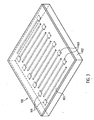
- Fig. 3 schematically displays a nanoelectronic device (100) in planar configuration employed for the characterization of the materials synthesized.
- the conducting electrodes (101) are mutually parallel and lay on an insulating substrate (102).
- the system is covered by a film (103) comprising the hybrid polyaniline-gold nanostructures.
- the planar configuration of the electronic device shown in Fig. 3 is an exemplary configuration for such a device.
- the nanoelectronic device can be fabricated in the multilayer configuration with the film comprising the hybrid nanostructures placed between overlapping electrodes.
- the planar configuration adopted for the characterization described in this subsection is particularly advantageous because it guarantees that the measured conductivity properties relate only to the film comprising the hybrid polyaniline-gold nanostructures and not to diffusion phenomena that may occur in the multilayer configuration.
- aluminum electrodes (101) are formed by a sputtering process on a precleaned glass substrate (102) (Agar Sputter Coater, Assing Scientific).
- the electrodes have a length of 5 mm, a width of 0.1 mm and a thickness of 70 nm. They are placed in a parallel planar configuration at a distance of 0.1 mm from each other.
- the hybrid polyaniline-gold nanostructures produced according to the process described in the previous subsection are dispersed in CHCl 3 by sonication (59 kHz) for 48 hours (Elma, D-78224, Transsonic Digitals).
- the polyaniline-gold nanostructures are dispersed in CCl 4 .
- aPS atactic polystyrene
- the content of polyaniline-gold nanostructures in the composite material ranges preferably from 1% to 10%.
- the so obtained composite material is deposited on the glass substrate (102) comprising the aluminum electrodes (101) by spin coating (Cee R Model 100, Brewer Science), so as to obtain a uniform film (103) with a thickness of 100 nm to 500 nm.
- the thickness and the roughness of the electrodes (101) and of the film (103) comprising the hybrid polyaniline-gold nanostructures are characterized by a profilometer (XP 1 Series Stylus Profiler, Ambios Technology).
- the results described in this subsection refer to a nanoelectronic device (100) fabricated according to the exemplary method described in the previous subsection.
- the content of polyaniline-gold nanostructures in the composite material employed to form the film (103) on the conducting electrodes (101) is 6.4%.
- the electronic properties are measured by a picoammeter coupled with a voltage source (Keithley 487).
- the temperature of the device is regulated and measured by a cryogenic probe station (Lakeshore Cryotronics) coupled with a temperature controller (Model 218, Janis Research Company).
- Figures 4 - 8 show the results obtained performing the measurements as described below between two adjacent electrodes (101) of the nanoelectronic device (100).
- the voltage scans are performed in a stepwise manner: the voltage is increased or decreased according to a step-like function with a step-height of 10 V and a step-width of 5 sec.
- Fig. 4 shows the I-V curve obtained by scanning the voltage applied between two adjacent electrodes of the nanoelectronic device from 0 V to +500 V and, subsequently, from +500 V to 0 V.
- the system exhibits a bistable electrical behavior shown by the hysteresis-like curve obtained by scanning the voltage.
- the voltage is increased from 0 V, the system exhibits low conductivity (OFF state).
- the current suddenly increases and the system displays high conductivity (ON state).
- the current measured in the high conductivity state is 5 to 6 orders of magnitude higher than the current in the low conductivity state.
- the ratio between the currents measured in the high and in the low conductivity states at the same voltage represents the ON/OFF ratio of the device.
- the bistable behavior is observed at high voltages (+240 V) because of the parallel planar configuration of the electronic device employed to characterize the hybrid polyaniline-gold nanostructures synthesized according to the preferred embodiment of the present invention described in the previous subsections.
- the electrodes are at a mutual distance which is about two orders of magnitude higher than the mutual distance between the electrodes in a typical multilayer configuration with the bistable material placed between overlapping electrodes. For this reason, the bistable behavior would be observed at about +2 V in a device with multilayer configuration.
- Fig. 5 shows the results of a test performed by submitting the device to repeated voltage scan cycles with the voltage ranging from 0 V to +500 V and then from +500 V to 0 V.
- the graph displays the results for three cycles.
- the bistable behavior is reproducible and the system follows the same hysteresis curve during the various voltage scan cycles.
- This test shows that the composite material comprising the hybrid polyaniline-gold nanostructures synthesized according to a preferred embodiment of the present invention is stable even when it undergoes several voltage cycles, and it exhibits a perfectly reproducible behavior.
- This property is important for several applications of the nanoelectronic device comprising the hybrid polyaniline-gold nanostructures.
- the ability of undergoing several ON/OFF switches under the same conditions is a fundamental property for the application of the nanoelectronic device for instance as non-volatile memory device.
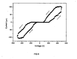
- Fig. 6 shows the results of a voltage cycle wherein the voltage is firstly increased from 0 V to + 500 V, then it is decreased from +500 V to -500 V, and, finally, it is increased from -500 V to 0 V.
- the system displays a perfectly symmetric bistable behavior with the switching between the OFF and ON states at about +240 V in the positive region of the applied voltage, and at about -240 V in the negative region.
- the intensity of the current measured in the conducting states is independent from the polarity of the applied voltage.
- Fig. 7 displays the results obtained by performing voltage scan cycles at different temperatures.
- the system displays the hysteresis-like I-V curves in a wide range of operating temperatures, showing that the bistable behavior is maintained even varying the temperature.
- the switching voltage increases by increasing the temperature because of the thermal expansion of the supporting polystyrene matrix.
- the area of the hysteresis cycles, on the contrary, is constant. Consequently the ON/OFF ratio of the device is independent on the operation temperature.
- Fig. 8 shows the resistivity of the system submitted to a voltage scan from -500 V to +500 V followed by a scan from +500 V to -500 V.
- the resistivity of the system varies by several orders of magnitude between the ON and the OFF states.
- the low value of the resistivity in the ON states is particularly advantageous because it is correlated with a low value of the switching voltage and it allows to minimize dissipation processes.
- the tests shown in the Figures 4 to 8 demonstrate that the hybrid polyaniline-gold nanostructures synthesized according to a preferred embodiment of the present invention display an excellent bistable electronic behavior, they are stable in a wide range of temperatures and they exhibit reproducible properties when submitted to repeated operation cycles.
- the bistability of the hybrid polyaniline-gold nanostructures synthesized according to a preferred embodiment of the present invention is characterized by a high ON/OFF ratio and by a low resistivity of the system in the ON state. These properties make the hybrid polyaniline-gold nanostructures synthesized according to a preferred embodiment of the present invention especially suitable for the application in non-volatile memory devices or field emission transistors.
- the preferred embodiment of the present invention described with respect to the preparation of hybrid polyaniline-gold nanostructures is extremely versatile and it is possible to apply it with a large variety of polymers and of nanoparticles.
- the method of producing hybrid nanostructures of the present invention can be, in fact, applied not only for the preparation of hybrid polymer-metal nanostructures, but also to produce hybrid polymer-fullerenes nanostructures or hybrid polymer-metal compounds nanostructures.
- several polymerizing methods can be employed for the synthesis of the polymeric structure in the presence of the dispersion of nanoparticles.
- by providing the nanoparticles with functionalizing groups it is possible to precisely tailor the interaction between the nanoparticles and the polymeric structure in the hybrid nanostructures.
- hybrid polymer-metal nanostructures or hybrid polymer-metal compounds nanostructures of the present invention can be applied to synthesize materials suitable for a wide range of applications.
- the hybrid nanostructures synthesized according to the method of the present invention can be employed for instance for sensors, light-emitting diodes, photovoltaic cells, catalysts, drug delivery systems and data storage systems.
Landscapes
- Chemical & Material Sciences (AREA)
- Engineering & Computer Science (AREA)
- Materials Engineering (AREA)
- Nanotechnology (AREA)
- Physics & Mathematics (AREA)
- Mathematical Physics (AREA)
- Theoretical Computer Science (AREA)
- Crystallography & Structural Chemistry (AREA)
- High Energy & Nuclear Physics (AREA)
- Inorganic Chemistry (AREA)
- Macromolecular Compounds Obtained By Forming Nitrogen-Containing Linkages In General (AREA)
- Compositions Of Macromolecular Compounds (AREA)
Description
- The present invention relates to the field of hybrid nanostructures. In particular, the present invention relates to a process to produce hybrid polymer-metal and polymer-metal compounds.
- Hybrid polymer-metal nanostructures, hybrid polymer-metal compounds and hybrid polymer-fullerenes nanostructures are a novel class of materials displaying distinctive physical and chemical properties. The properties of these materials are noticeably different from those of their single components, and, for this reason, hybrid nanostructures are currently under thorough investigation. These materials represents promising solutions in a wide range of fields of application, such as electronics, catalysis and biotechnology.
- One of the main properties observed in some hybrid polymer-metal nanostructures is the electrical bistability. This phenomenon describes the presence of two states with different conductivities at the same applied voltage. One of the states displays low conductivity (OFF state), while the other is characterized by high conductivity (ON state). The ratio between the currents obtained at the same applied voltage in the two different states is called ON/OFF ratio of the system. The voltage at which the transition between the two states occurs is referred to as the switching voltage of the system. Once the system is in one of the two states, it remains steadily in this state until a voltage equal or higher than the switching voltage is applied. It is, thus necessary to apply a voltage higher than the switching voltage to a system in the OFF state to force it into the ON state. On the contrary, once the system is in the ON state, it is necessary to apply a negative voltage as high as the switching voltage to restore the OFF state. For this reason, hybrid polymer-metal nanostructures are ideal candidates for the formation of non-volatile memory devices, i.e. devices capable of retaining stored information even without the supply of power.
- Hybrid polymer-fullerenes nanostructures are a novel class of materials whose properties are still under investigation. This hybrid nanostructures are formed by a polymeric structure decorated by fullerenes. Fullerenes are a family of carbon allotropes (molecules composed entirely of carbon) in the form of a hollow sphere, ellipsoid, tube or plane. Particularly relevant for the formation of hybrid polymer-fullerenes nanostructures are, for instance, buckyballs (spherical fullerenes), carbon nanotubes (cylindrical fullerenes), nano-onions (spherical particles based on multiple carbon layers surrounding a buckyball core), linked ball-and-chain dimers and fullerene rings.
- Hybrid polymer-metal compounds nanostructures are formed by a polymeric structure decorated by nanoparticles formed by metal compounds. These nanoparticles formed by metal compounds may also have a non metallic nature.
- One of the critical aspects of hybrid nanostructures is their synthesis process. The properties of these materials depend strongly, in fact, on the synthesis process employed to produce them. It is of major importance to control precisely the geometry of the hybrid polymer-metal nanostructures, hybrid polymer-metal compounds nanostructures and polymer-fullerenes nanostructures. The structure and the dimensions of the polymeric phase play an important role in the properties of the final hybrid nanostructures such as the stability of the material. On the other hand, it is extremely important to control the size and the distribution of the metal particles and of the fullerenes. It is known, in fact, that the electrical bistability is strongly dependent on the size of the nanoparticles and that, if the nanoparticles exceeds a certain size, the metallic nature of the particles dominates the properties of the system. In this case, the system does not exhibit electrical bistability, but it can be switched from the OFF state to the ON state only once, and then it remains in this state displaying an ohmic behavior [1].
- According to the methods known in the prior art, hybrid polymer-metal nanostructures are produced by redox reactions between the polymers and precursor materials for the metallic particles, typically ionic metal compounds (salts). In [1] the first step of the preparation process is the synthesis of the polymeric structure. Subsequently, the polymeric structure is let react with a metal salt (for instance tetrabromoaurate or chloroaurate), In [2], the metal salt (chloroaurate) is employed as the oxidant for the polymerization reaction of the monomer.
- A further example of direct reaction between polyaniline nanafibers and oxidizing metal ions such as Au3+ and Ag+ can be found in Pure Appl. Chem, Vol 78, , by J. Huang. In Nano Letters, Vol. 5, No. 6, pp. 1077-1080 (200%, a digital memory device is disclosed based on the nanofibers obtained with the method described In the previous paper.
- In all these cases it is extremely difficult to control the size and the distribution of the metal particles. Moreover, it is not possible to control and engineer the interaction between the metal particles and the polymeric structure.
- Finally, M.M. Oliveira and colleagues (J. Phys. Chem. B, Vol. 110, pp. 17063-17069 (2006)) report on the development of a process for synthesizing hybrid silver nanopartiCles/polyaniline nanosheets.
- In view of the mentioned problems incurred in the synthesis process of hybrid polymer-metal nanostructures, hybrid polymer-metal compounds nanostrucures or hybrid polymer-fullerenes nanostructures, it is an object of the present invention to provide a method of producing hybrid polymer-metal nanostructures and hybrid polymer-metal compounds nanostructures allowing to overcome these problems. In particular, it is an object of the present invention to provide a versatile method of producing hybrid polymer-metal nanostructures, hybrid polymer-metal compounds nanostructures wherein a large variety of polymers, metals and metals compounds can be chosen to form the hybrid nanostructures. Moreover, it as an object of the present invention to provide a method which allows to engineer the chemical and physical properties of the hybrid polymer-metal nanostructures and hybrid polymer-metal compounds nanostructures in a controlled way. More in particular, it is an object of the present invention to provide a method that allows to control the size distributions parameters of the metal particles in the hybrid nanostructures with high accuracy. It is a further object of the present invention to provide a method that allows to control the nature and the properties of the interaction between the metal nanoparticles and the polymeric structure. It is a further object of the present invention to provide a method that allows to engineer the structure of the polymer material in the hybrid polymer-metal nanostructures and hybrid polymer-metal compounds nanostructures. Moreover, it is an object of the present invention to provide a method of producing hybrid polymer-metal nanostructures and hybrid polymer-metal compounds nanostructures that can be performed in conjunction with a large variety of polymerization processes necessary to form the polymeric structure in the hybrid material.
- It is a further object of the present invention to provide electronic devices comprising hybrid polymer-metal nanostructures, hybrid polymer metal compounds nanostructures. Moreover, it is an object of the present invention to provide several kinds of nanodevices suitable for several kinds of applications such as non volatile memory devices, field effect transistors, sensors. light emission diodes, photovoltetic cells, drug delivery systems, data storage and spintronics.
- According to the present invention, there is provide a method of producing hybrid polymer-metal nanostructures or hybrid polymer-metal compounds nanostructures which is based on the inventive concept of providing first a dispersion of metal nanoparticles, or of metal compounds nanoparticles and subsequently polymerizing the polymer structure in the presence of said dispersion of metal nanopartides, or of metal compounds nanoparticles as defined in
claim 1. - Preferred embodiments are given In the subclaims as well as the following specification,
-
-
Fig. 1 shows the thermogravimetric analysis (TGA) of hybrid polyaniline-gold nanostructures synthesized according to a preferred embodiment of the present invention. -
Fig. 2 shows the particles size distribution curve for gold nanoparticles in a hybrid polyaniline-gold nanostructure synthesized according to a preferred embodiment of the present invention. -
Fig. 3 displays a nanoelectronic device in planar configuration including a film comprising hybrid polymer-metal nanostructures synthesized according to a preferred embodiment of the present invention. -
Fig. 4 shows the I-V curve obtained by scanning the voltage applied between two adjacent electrodes of the nanoelectronic device ofFig. 3 . -
Fig. 5 shows the I-V curves obtained by scanning repeatedly the voltage applied between two adjacent electrodes of the nanoelectronic device ofFig. 3 . -
Fig. 6 shows the I-V curve obtained by scanning the voltage applied between two adjacent electrodes of the nanoelectronic device ofFig. 3 both for positive and negative values of the polarity. -
Fig. 7 shows the I-V curves obtained by scanning the voltage applied between two adjacent electrodes of the nanoelectronic device ofFig. 3 for four different values of the operating temperature. -
Fig. 8 shows the resistivity of the nanoelectronic device ofFig. 3 measured during a voltage scan between -500 V and +500 V. - In a preferred embodiment of the present invention, a method of producing hybrid polymer-metal nanostructures and hybrid pollymer-metal compounds nanostructure is provided, the method comprising the steps of providing a dispersion of metal nanoparticles, of of metal compounds nanoparticles in an aqueous phase and polymerizing a conducting polymer in the presence of said dispersion.
- In a further preferred embodiment of the present invention, a method of producing hybrid polymer-metal nanostructures is provided, wherein the step of providing a dispersion of metal nanoparticles further comprises the step of functionalizing the metal nanoparticles with an organic ligand. Functionalizing the metal nanoparticles with an organic ligand allows to control the interaction between the metal nanoparticles and the polymeric structure in the final hybrid polymer-metal nanostructure. The interaction between the metal nanoparticles and the polymer structure is fundamental for the stability of the hybrid nanostructure. It is possible to choose organic ligands that allow for the stability of the hybrid nanostructure for instance over wide range of temperatures and other operating conditions (pressure, humidity, etc). Moreover, the interaction between the metal nanoparticles and the polymer structure is one of the fundamental parameters determining the physical and chemical properties of the hybrid material. Providing the functionalized metal nanoparticles in the hybrid polymer-metal material with organic ligands displaying specific properties allows to tailor the hybrid polymer-metal material for several kinds of applications, such as non-volatile memory devices, field effect transistors, sensors, light emitting diodes and photovoltaic cells. Furthermore, the organic ligands can play the fundamental role of protection for the nanoparticles, and they can prevent on one hand the segregation of the nanoparticles or, on the other hand, the aggregation into larger clusters. There are several kinds of organic ligands suitable to functionalize the metal nanoparticles: the metal nanoparticles can be coated for instance with alkanethiols and alkanethiol derivatives. Examples are: thiols (dodecanethiol, naphtalenethiol, benzylthiol, phosphinethiol, amido-acetyl alkanethiol, thioglycerol, aminothiophenol); DNA; mercaptobenzoic acid; mercaptohexanol; sulfonated polystyrene or paramethylstyrene; polypeptides; hyperbranched polymers and polyelectolytes; dodecylamine; amino-phosphate; mercaptoalkyl alcoxysilane; mercaptoethanol; mercaptosilanes; mercaptocarboxylic acids (mercaptoacetic acid, mercaptopropionic acid, mercaptosuccinic acid, mercaptobenzoic acid, mercaptoundecanoic acid).
- In yet another preferred embodiment of the present invention, the metal nanoparticles are made of at least one of gold, cobalt, nickel, ruthenium, osmium, molybdenum, tungsten, yttrium, lutetium, copper, manganese, chromium, zinc, palladium, silver, platinum, tin, tellurium, bismuth, germanium, antimony, aluminum, indium, selenium, cadmium, gadolinium, hafnium, magnesium, titanium, lanthanum, cerium, praseodymium, neodymium, terbium, dysprosium, holmium, erbium iridium, rhodium, iron, titanium, lead, zirconium, vanadium and alloys composed of these metals. Suitable precursors are metal compounds such as tetrabromoaurate, chloroaurate, palladium nitrate, cadmium sulfide, cobaltosic oxide, lead sulfide, zinc sulfide, titanium oxide, iron oxides, zirconium oxide, iron chloride, tungsten and molybdenum acids. The choice of the metal can be made in view of the desired properties of the hybrid polymer-material nanostructures. Besides metals suitable for the application of the hybrid polymer-metal nanostructures for electronic devices, it is possible to choose metals with specific catalytic activities in order to employ the hybrid materials in catalysis processes.
- The nanoparticles may also be made of metal compounds such as: CdTe, CdSe, CdS, ZnS, GaN, Ag2S. CUS2, CuTe, CuSe.
- The particle size distribution parameters of the metal nanoparticles in the hybrid polymer-metal nanostructures are fundamental for determining the properties of the hybrid material. In the method of producing polymer-metal nanostructures of the present invention, these parameters are highly controllable, and allow to tailor the hybrid material to several kinds of applications.
- In a particularly favorable embodiment of the present invention, the metal nanoparticles in the hybrid polymer-metal nanostructure have a mean particle size of 25 nm or less.
- In a further embodiment of the present invention, the metal nanaparticles In the hybrid polymer-metal nanostructure have a size uniformity of 2 nm or less.
- According to the present disclosure, the fullerenes in the hybrid polymer-fullerenes nanostructures are at least one of buckyballs, carbon nanotubes, nano-onions, linked ball-and-chain dimers and fullerene rings.
- In the present invention, the conducting polymer forms nanofibers or nanoparticles. In a further preferred embodiment of the present invention the nanofibers have a mean diameter of 100 nm or less. In yet another preferred embodiment of the present invention, the nanofibers have a length ranging from at least 50 nm to 100 µm. In a further favorable embodiment of the present invention the nanofibers have a mean diameter of 100 nm or less and a length ranging from at least 50 nm to 100 µm.
- In a further preferred embodiment of the present invention, the conducting polymer is polyaniline (PANI). Polyaniline is a conducting polymer with unique properties. It is easily synthesized and, for this reason, it is available at low costs. It is highly stable in several environmental conditions. Its electrical and optical properties are easily tunable with simple acid/base doping/cledoplng processes. For these reasons the employment of polyaniline in hybrid polymer-metal or hybrid polymer-fullerenes nanostructures is particularly advantageous, for instance, for their application in sensor or electronic devices. Moreover, it is possible to synthesize polyaniline in the form of nanofibers which can form the polymeric structure in the hybrid polymer-metal nanostructures, or in the hybrid polymer-metal compounds nanostructures or in the hybrid polymer-fullerenes nanostructures. According to the present invention, the structural properties of the polyaniline nanofibers (such as average length and average diameter) can be precisely controlled. The diameter of the PANI nanofibers is preferably 60 nm or less. The length of the PANI nanofibers is preferably at least 50 nm. Moreover, polyaniline can be synthesized in the form of nanoparticles which can form the polymeric structure in the hybrid nanostructures.
- Other examples of conducting polymers are for instance polypyrrole, polyvinylpyrrolidine. polyurethane, polythiophene, polyfluorene.
- The conducting polymers can be synthesized in several forms such as conducting polymer nanostructures like nano-rods, nanotubes, nano-wires, nanoparticles and nanofibers.
- The method of producing hybrid polymer-metal nanostructures, hybrid polymer-metal compounds nanostructures or hybrid polymer-fullerenes nanostructures disclosed herewith can be performed in conjunction with a large variety of polymerization processes necessary to form the polymeric structure in the hybrid material.
- In a parucularly advantageous embodiment disclosed herewith, the step of polymerizing a conducting polymer in the presence of the metal nanoparticles dispersion, or of metal compounds nanoparticles dispersion or of the fullerenes dispersion is performed by interfacial polymerization. In this process, the polymerization reaction takes place at the interface between an aqueous and an organic phase in a biphase system. The polymer formed at the interface diffuse in the aqueous phase allowing for the continuous availability of reaction sites at the interface. In this exemplary embodiment of the present invention, the aqueous phase comprises the dispersion of metal nanoparticles or of metal compounds nanoparticles or of fullerenes. In a particular embodiment of the present invention, the preparation of the aqueous phase for the interface polymerization process comprises the steps of synthesizing metal nanoparticles, functionalizing the metal nanoparticles with an organic ligand, preparing a mixture of water and surfactant, dispersing the functionalized metal nanoparticles In the mixture of water and surfactant, treating the system with ultrasonication, adding an initiator agent, adding a doping agent Examples of surfactants are Dodecylbenzenesulfonic acid, Sodium dodecylsutfate, Ammonium lauryl sulfate and other alkyl sulfate salts, Sodium laureth sulfate, Akyl benzene sulfonate, Cetyl trimethylammonium bromide, Cetylpyridinium chloride, Polyethoxylated tallow amine, Benzalkonium chloride. Benzethonium chloride, Dodecyl betaine, Dodecyl dimethylamlne oxide, Cocamldopropyl betaine. Cocoampho glycinate, Alkyl poly(ethylene oxide), Copolymers of poly(ethylene oxide) and poly(propylene oxide). Alkyl polyglucosides including: Octyl glucoside. Decyl maltoside, Cetyl alcohol, Oleyl alcohol, Cocamide MEA, Cocamide DEX and Cocamide TEA and silicone-based surfactants.
- Examples of initiator agents are ammonium persuffate, potassium bichromate, hydrogen peroxide, ferric chloride, Na2S2O8 and K2S2O8. Ce(SO4)2 KMnO4, KBrO3, KlO3, R2O2. V2Os, NaVO3, NaClO and metallic ions. Examples of doping agents are (1S)-(+)-camphorsulfonic acid, (1R)-(-)-camphorsuffonic acid, (+)-camphorsulfonic acid, (±)-camphorsulfonic acid, L-tartaric acid and D-tartaric acid, HCl, H2SO4, HNO3, HClO4. H3PO4, acetic acid, formic acid, methanesulfonic acid, ethylsulfonic acid, toluenesulfonic acid, methytbenzene sulfonic acid, naphtalene sulfonic acid, dinitronaphtol sulfonic acid and polystyrene sulfonic acid. The preparation of the organic solution comprises the step of mixing the monomers with a reagent such as CCl4, benzene, toluene, methylene chloride, xylene, hexane, diethylether, dichloromethane, carbon disufide tetrahydrofuran, chloroform, methylene chloride, N-methyl-2-pyrrolidinone, or other polar aprotic solvent dimethyl acetamide, dimethyl formamide, ethyl acetate or other ester solvent and alcohols. The aqueous phase is slowly added to the organic phase to form the biphasic system. The organic phase may comprise aniline, methylaniline, ethylaniline, alkoxyaniline e dialkoxyaniline, but other carbon-based organic monomers can be used, such as pyrrole, thiophene, toluidine, anisidine.
- In yet another preferred embodiment disclosed herewith, the step of polymerizing a conducting polymer in the presence of the metal nanoparticles dispersion or of the metal compounds nanoparticles dispersion or of the fullerenes dispersion is performed by one of rapidly mixed reactions such as disclosed in [3], dilute polymerization such as disclosed in [4], sonication such as disclosed in [5], electrochemical polymerization or chemical polymerization reactions in the presence of structural directing agents such as templates like membranes or porous materials. Each of these processes can be performed in the presence of a dispersion of metal nanoparticles or of metal compounds nanoparticles or of fullerenes allowing for the versable synthesis of hybrid polymer-metal nanostructures, hybrid polymer-metal compounds nanostructures or of hybrid polymer-fullerenes nanostructures according to a preferred embodiment of the present invention.
- In yet a further embodiment disclosed herewith, a hybrid nanostructure is provided, said hybrid nanostructune being obtainable with the producing method according to the present invention.
- In a further embodiment disclosed herewith, an electronic device comprising a layer including the hybrid nanostructure obtainable with the producing method according to the present invention is provided.
- In yet a further embodiment disclosed herewith, an electronic device comprising a layer including the hybrid nanostructures obtainable with the producing method according to the present invention and formed by a composite material comprising hybrid polymer-metal or polymer-fullerenes nanostructures dispersed in a polymeric matrix is provided. Examples of polymers suitable for the formation of the polymeric matrix are polystyrene, polyvinyl alcohol, polyvinyl chloride, poly-methyl methacrylate, cross-linked poly-4-vinylphenol, polyethylene oxide, poly(N-ethyl-2-vinylcarbazole), polyolefines, polyamides polyesters, polyester ketone, polyimides, polyurethanes, polychlorotrifluoroethylene. The polymeric matrix is of fundamental importance for the employment of the hybrid polymer-metal nanostructures and polymer-fullerenes nanostructures in nanodevice applications. The polymeric matrix may function as supporting matrix for the hybrid nanostructures. The polymeric matrix may confer high homogeneity and stability to the system. Because of the homogeneity of the system formed by hybrid nanostructures dispersed in a supporting polymeric matrix, a higher control on the scaling and the modeling of the nanodevices is achieved. Moreover, even if the primary role of the supporting polymeric matrix is that of forming an insulating matrix that prevents shorting out of the nanodevice, it is also possible to control the performances of the device by properly controlling the chemical composition of the supporting matrix. The physical properties of the supporting matrix such as the dielectric constant, the density, the thermal and mechanical properties contribute in fact to the performances of the device. By properly choosing the supporting matrix in which the hybrid polymer-metal and polymer-fullerenes nanostructures are dispersed, it is, thus, possible to tailor the nanodevice to several kinds of applications, such as non volatile memory devices, field effect transistors (FET), sensors, light emission diodes (LED), photovoltaic cells, drug delivery systems, data storage, spintronic and the like.
- In order to form the composite material comprising the hybrid polymer-metal nanostructures, the hybrid polymer-metal compounds nanostructures or the hybrid polymer-fullerenes nanostructures in the supporting polymeric matrix, various amounts of hybrid nanostructures synthesized according to the method of the present invention may be dispersed in a solution of the supporting polymer. The content of hybrid nanostructures in the composite material may preferably range from 1% to 10%. The dispersion of hybrid nanostructures in a solution of the supporting polymer may be performed by techniques known in the art such as sonication or stirring techniques. The composite material may be coated on the electrodes of the nanodevice by known coating techniques such as spin-coating, spray coating, drop coating, coating techniques employed in association with photolithography masking techniques and the like.
- In the following, the present invention is described with reference to a preferred embodiment as illustrated in the following detailed description. Accordingly, this description is to be construed as illustrative only and is for the purpose of teaching those skilled in the art the general manner of carrying out the present invention.
- The following section is organized as follows: the first subsection illustrates the details of the synthesis process of a preferred polymer-metal hybrid nanostructure according to a preferred embodiment of the present invention, the second subsection describes the fabrication of a nanoelectronic device comprising the polymer-metal hybrid nanostructure synthesized according to the preferred embodiment described in the first subsection, finally, the third subsection shows the properties of the nanoelectronic device fabricated according to the exemplary procedure described in the second subsection.
- In the following subsection the method of producing polyaniline nanofibers decorated with gold nanoparticles according to a preferred embodiment of the present invention is described.
- In the first step of the preferred production method, dodecanethiolate-functionalized gold nanoparticles with 3-4 nm mean particle size are synthesized according to a standard procedure such as disclosed in [6]. In particular, 0.79 g of HAuCL4·3H2O in 50 mL of deionized water are added to a solution of 2.8 g of tetraoctylammonium bromide in 160 mL of toluene. After isolating the organic phase, the desired amount of dodecanethiol is added and the resulting solution is stirred for 10 minutes. The Au:dodecanethiol ratio determines the mean particle size of the gold nanoparticles as shown for instance in [6]. 0.77 g of NaBH4 in 50 mL of deionized water are added over periods of 5 minutes. The solution is stirred at room temperature for 3.5 hours. The organic phase is collected and the solvent is removed by evaporation at 50°C. The product is suspended in 150 mL of ethanol, sonicated, collected on a glass filtration frit, washed with ethanol and acetone and finally dried in vacuum.
- In the second step, a dispersion of the dodecanethiolate-functionalized gold nanoparticles in deionized water and dodecylbenzenesulfonic acid (DBSA) is provided.
- For this purpose, 20 mg of the dodecanethiolate-functionalized gold nanoparticles synthesized as described above are added to a solution formed by 200 mL of deionized water and DBSA so that the Au:DBSA ratio is 1:2.5. The obtained dispersion is sonicated (20 kHz) for 48 hours. The dispersion displays the typical gray color.
- In the third step of the exemplary production method, polyaniline nanofibers are polymerized in the presence of the dispersion of dodecanethiolate-functionalized gold nanoparticles provided in the second step. In this exemplary production method the polymerization is performed by an interfacial polymerization process. For this purpose, 1.127 g of ammonium persulfate (APS) (initiator agent) and 47.41 g of camphorsulfonic acid (CSA) (doping agent) are added to the dispersion of dodecanethiolate-functionalized gold nanoparticles. The dispersion of dodecanethiolate-functionalized gold nanoparticles including the initiator and the doping agents is slowly added to an organic solution made of 200 mL of CCl4 and 2 mL of Aniline. The dispersion and the organic solution form an interface and the system has a biphasic nature. The so prepared biphasic reaction mixture is sealed off, and after a reaction time of 24 hours the polymerization process is completed. The polymerization process occurs at the interface between the organic solution and the aqueous dispersion of nanoparticles. The as-prepared polyaniline is in a hydrophilic form and for this reason it diffuses away from the interface into the aqueous region giving rise to the formation of nanofibers: the diffusion of polyaniline from the interface towards the aqueous region allows for the continuous availability of reaction sites at the interface and, at the same time, prevents the overgrowth of irregularly shaped agglomerates of the polymer. During this polymerization process, the dodecanethiolate-functionalized gold nanoparticles dispersed in the aqueous region are trapped by the growing polyaniline nanofibers. Because of this growth mechanism, some of the dodecanethiolate-functionalized gold nanoparticles are trapped inside the nanofibers, while others are bound on the external surface of the polymer nanostructures. When the polymerization process is completed, the aqueous region comprises the hybrid polymer-metal nanostructures and displays the typical green color. At this point the aqueous phase is separated from the organic phase and it is filtered in vacuum. The residue obtained from the filtration process is further washed with deionized water and acetone and finally dried in vacuum at a temperature of 80 °C. The final product of this process consists in the hybrid polyaniline-gold nanostructures formed by nanofibers of polyaniline decorated with gold nanoparticles.
-
Fig. 1 shows the thermogravimetric analysis (TGA 2950 Thermogravimetric Analyzer, TA Instruments) of the hybrid polyaniline-gold nanostructures synthesized according to the above described production method. The thermal scan is performed in a nitrogen atmosphere between 30°C and 800°C with a heating rate of 10°C/min. Curves (a) and (b) correspond to samples of pure dodecanethiolate-functionalized gold nanoparticles and pure polyaniline fibers, respectively, while curve (c) relates to the hybrid polyaniline-gold nanostructures. Curve (a) shows a single degradation feature between 190°C and 275°C corresponding to the decomposition of the dodecanethiol. Curve (b) measured on the pure polyaniline nanofibers displays two degradation features: the first between 200°C and 350°C, the second between 400°C and 550°C. The first feature corresponds to the decomposition of the camphorsulfonic acid, while the second corresponds to the deterioration of the structure of the nanofibers. Curve (c) measured on the hybrid polyaniline-gold nanostructures displays a single degradation features between 200°C and 350°C corresponding to the decomposition of the camphorsulfonic acid, and a smooth degradation trend towards high temperature due to the slow diffusion of gas through the nanofibers comprising the gold nanoparticles. The final residue (65%) is higher than the residue in the case of pure polyaniline nanofibers (40%). These results show that the majority of gold nanoparticles are trapped and protected inside the polyaniline nanofibers structure and that the hybrid polyaniline-gold nanostructure are formed by about 25% of gold. -
Fig. 2 shows the particles size distribution curve of the gold nanoparticles obtained by the analysis of Transmission Electron Microscopy (Jeol JEM 1220 Microscope) images of the hybrid nanostructures. The mean particle size is 3.6 nm with a uniformity of 3.6 ± 1 nm. The uniformity is calculated by considering the standard deviation of the data. - Moreover, TEM images of the hybrid nanostructures show that the diameter of the polyaniline nanofibers measures 40 to 50 nm, and their length ranges from about 100 nm to about 10 µm.
- The following subsection describes the fabrication of a nanoelectronic device employed for the characterization of the hybrid polyaniline-gold nanostructures produced according to the exemplary embodiment of the present invention described in the previous subsection.
-
Fig. 3 schematically displays a nanoelectronic device (100) in planar configuration employed for the characterization of the materials synthesized. The conducting electrodes (101) are mutually parallel and lay on an insulating substrate (102). The system is covered by a film (103) comprising the hybrid polyaniline-gold nanostructures. The planar configuration of the electronic device shown inFig. 3 is an exemplary configuration for such a device. Alternatively, the nanoelectronic device can be fabricated in the multilayer configuration with the film comprising the hybrid nanostructures placed between overlapping electrodes. The planar configuration adopted for the characterization described in this subsection is particularly advantageous because it guarantees that the measured conductivity properties relate only to the film comprising the hybrid polyaniline-gold nanostructures and not to diffusion phenomena that may occur in the multilayer configuration. - In the first step of the exemplary fabrication procedure, aluminum electrodes (101) are formed by a sputtering process on a precleaned glass substrate (102) (Agar Sputter Coater, Assing Scientific). The electrodes have a length of 5 mm, a width of 0.1 mm and a thickness of 70 nm. They are placed in a parallel planar configuration at a distance of 0.1 mm from each other.
- The hybrid polyaniline-gold nanostructures produced according to the process described in the previous subsection are dispersed in CHCl3 by sonication (59 kHz) for 48 hours (Elma, D-78224, Transsonic Digitals). Alternatively, the polyaniline-gold nanostructures are dispersed in CCl4. Subsequently, atactic polystyrene (aPS) is added to the obtained dispersion at 80°C for 30 minutes in order to obtain a composite material formed by hybrid polyaniline-gold nanostructures dispersed in a supporting polystyrene matrix. The content of polyaniline-gold nanostructures in the composite material ranges preferably from 1% to 10%.
- The so obtained composite material is deposited on the glass substrate (102) comprising the aluminum electrodes (101) by spin coating (CeeR Model 100, Brewer Science), so as to obtain a uniform film (103) with a thickness of 100 nm to 500 nm.
- The thickness and the roughness of the electrodes (101) and of the film (103) comprising the hybrid polyaniline-gold nanostructures are characterized by a profilometer (
XP 1 Series Stylus Profiler, Ambios Technology). - The results described in this subsection refer to a nanoelectronic device (100) fabricated according to the exemplary method described in the previous subsection. The content of polyaniline-gold nanostructures in the composite material employed to form the film (103) on the conducting electrodes (101) is 6.4%. The electronic properties are measured by a picoammeter coupled with a voltage source (Keithley 487). The temperature of the device is regulated and measured by a cryogenic probe station (Lakeshore Cryotronics) coupled with a temperature controller (Model 218, Janis Research Company).
-
Figures 4 - 8 show the results obtained performing the measurements as described below between two adjacent electrodes (101) of the nanoelectronic device (100). In all the measurements, the voltage scans are performed in a stepwise manner: the voltage is increased or decreased according to a step-like function with a step-height of 10 V and a step-width of 5 sec. -
Fig. 4 shows the I-V curve obtained by scanning the voltage applied between two adjacent electrodes of the nanoelectronic device from 0 V to +500 V and, subsequently, from +500 V to 0 V. The system exhibits a bistable electrical behavior shown by the hysteresis-like curve obtained by scanning the voltage. When the voltage is increased from 0 V, the system exhibits low conductivity (OFF state). At about +240 V, the current suddenly increases and the system displays high conductivity (ON state). Once the ON state is established at high voltage, it is stable even decreasing the voltage towards 0 V. The current measured in the high conductivity state is 5 to 6 orders of magnitude higher than the current in the low conductivity state. The ratio between the currents measured in the high and in the low conductivity states at the same voltage represents the ON/OFF ratio of the device. - The bistable behavior is observed at high voltages (+240 V) because of the parallel planar configuration of the electronic device employed to characterize the hybrid polyaniline-gold nanostructures synthesized according to the preferred embodiment of the present invention described in the previous subsections. In the parallel configuration the electrodes are at a mutual distance which is about two orders of magnitude higher than the mutual distance between the electrodes in a typical multilayer configuration with the bistable material placed between overlapping electrodes. For this reason, the bistable behavior would be observed at about +2 V in a device with multilayer configuration.
-
Fig. 5 shows the results of a test performed by submitting the device to repeated voltage scan cycles with the voltage ranging from 0 V to +500 V and then from +500 V to 0 V. The graph displays the results for three cycles. The bistable behavior is reproducible and the system follows the same hysteresis curve during the various voltage scan cycles. This test shows that the composite material comprising the hybrid polyaniline-gold nanostructures synthesized according to a preferred embodiment of the present invention is stable even when it undergoes several voltage cycles, and it exhibits a perfectly reproducible behavior. This property is important for several applications of the nanoelectronic device comprising the hybrid polyaniline-gold nanostructures. The ability of undergoing several ON/OFF switches under the same conditions is a fundamental property for the application of the nanoelectronic device for instance as non-volatile memory device. -
Fig. 6 shows the results of a voltage cycle wherein the voltage is firstly increased from 0 V to + 500 V, then it is decreased from +500 V to -500 V, and, finally, it is increased from -500 V to 0 V. The system displays a perfectly symmetric bistable behavior with the switching between the OFF and ON states at about +240 V in the positive region of the applied voltage, and at about -240 V in the negative region. The intensity of the current measured in the conducting states is independent from the polarity of the applied voltage. -
Fig. 7 displays the results obtained by performing voltage scan cycles at different temperatures. The system displays the hysteresis-like I-V curves in a wide range of operating temperatures, showing that the bistable behavior is maintained even varying the temperature. The switching voltage increases by increasing the temperature because of the thermal expansion of the supporting polystyrene matrix. The area of the hysteresis cycles, on the contrary, is constant. Consequently the ON/OFF ratio of the device is independent on the operation temperature. -
Fig. 8 shows the resistivity of the system submitted to a voltage scan from -500 V to +500 V followed by a scan from +500 V to -500 V. The resistivity of the system varies by several orders of magnitude between the ON and the OFF states. The low value of the resistivity in the ON states is particularly advantageous because it is correlated with a low value of the switching voltage and it allows to minimize dissipation processes. - The tests shown in the
Figures 4 to 8 demonstrate that the hybrid polyaniline-gold nanostructures synthesized according to a preferred embodiment of the present invention display an excellent bistable electronic behavior, they are stable in a wide range of temperatures and they exhibit reproducible properties when submitted to repeated operation cycles. The bistability of the hybrid polyaniline-gold nanostructures synthesized according to a preferred embodiment of the present invention is characterized by a high ON/OFF ratio and by a low resistivity of the system in the ON state. These properties make the hybrid polyaniline-gold nanostructures synthesized according to a preferred embodiment of the present invention especially suitable for the application in non-volatile memory devices or field emission transistors. - The preferred embodiment of the present invention described with respect to the preparation of hybrid polyaniline-gold nanostructures is extremely versatile and it is possible to apply it with a large variety of polymers and of nanoparticles. The method of producing hybrid nanostructures of the present invention can be, in fact, applied not only for the preparation of hybrid polymer-metal nanostructures, but also to produce hybrid polymer-fullerenes nanostructures or hybrid polymer-metal compounds nanostructures. Moreover, several polymerizing methods can be employed for the synthesis of the polymeric structure in the presence of the dispersion of nanoparticles. Furthermore, by providing the nanoparticles with functionalizing groups, it is possible to precisely tailor the interaction between the nanoparticles and the polymeric structure in the hybrid nanostructures.
- For these reasons, the method of producing hybrid polymer-metal nanostructures or hybrid polymer-metal compounds nanostructures of the present invention can be applied to synthesize materials suitable for a wide range of applications. The hybrid nanostructures synthesized according to the method of the present invention can be employed for instance for sensors, light-emitting diodes, photovoltaic cells, catalysts, drug delivery systems and data storage systems.
-
- [1] R. J. Tseng et al., Nano Letters, 5 (2005) 1077
- [2] Y. Wang et al., Langmuir, 21 (2005) 833
- [3] J. X. Huang, R. B. Kaner, Angew. Chem. Int. Ed, 43 (2004) 5817
- [4] N. Chiou, A. J. Epstein, Advanced Materials, 17 (2005) 1679
- [5] X. Jing et al., Ultrasonics Sonochemistry, 14 (2007) 75
- [6] M.J. Hostetler et al., Langmuir, 14 (1998) 17
Claims (7)
- A method of producing hybrid polymer-metal nanostructures or hybrid polymer-metal compounds nanostructures, the method comprising the steps of,
providing a dispersion of metal nanoparticies or of metal compounds nanoparticles in an aqueous phase,
preparing an organic solution by mixing the monomers of a conducting polymer with a reagent such as CCl4, benzene, toluene, methylene, chloride, xylene, hexane, diethylether, dichloromethane, carbon disulfide, tetrahydrofuran, chloroform, methylene chloride, N-methyl-2-pyrrolidinone, a polar aprotic solvent, dimethyl acetamide, dimethyl formamide, ethyl acetate, an ester solvent, an ester alcohol,
adding said dispersion of metal nanoparticles or of metal compounds nanoparticles in said aqueous phase to said organic solution so as to form a biphasic system comprising an interface between said aqueous phase and said organic solution,
polymerizing said monomers of said conducting polymer in the presence of said dispersion,
wherein said step of polymerizing said monomers of said conducting polymer in the presence of said dispersion is performed by interfacial polymerization so that said conducting polymer forms nanofibers or nanoparticles. - The method of claim 1, wherein said step of providing metal nanoparticles in an aqueous phase further comprises the step of functionalizing said metal nanoparticles with an organic ligand.
- The method of any one of the preceding claims, wherein said metal nanoparticles are made of at least one of gold, palladium, silver, platinum, copper, titanium, cobalt.
- The method of any one of the preceding claims, wherein said metal nanoparticles have a mean particle size of 25 nm or less.
- The method of any one of the preceding claims, wherein said metal nanoparticles have a size uniformity of 2 nm or less.
- The method of one of claims 1 to 5, wherein said nanofibers have a mean diameter of 100 nm or less, or a length ranging from at least 50 nm to 100 µm, or a mean diameter of 100 nm or less and a length ranging from at least 50 nm to 100 µm.
- The method of any one of the preceding claims, wherein said conducting polymer is polyaniline.
Priority Applications (2)
| Application Number | Priority Date | Filing Date | Title |
|---|---|---|---|
| EP08010990.3A EP2136421B1 (en) | 2008-06-17 | 2008-06-17 | New synthesis of hybrid polymer-metal nanostructures and hybrid polymer-metal compounds nanostructures for nanodevice applications |
| PCT/EP2009/004375 WO2009153035A1 (en) | 2008-06-17 | 2009-06-17 | New synthesis of hybrid polymer-metal nanostructures, hybrid polymer-metal compounds nanostructures and hybrid polymer- fullerenes nanostructures for nanodevice applications |
Applications Claiming Priority (1)
| Application Number | Priority Date | Filing Date | Title |
|---|---|---|---|
| EP08010990.3A EP2136421B1 (en) | 2008-06-17 | 2008-06-17 | New synthesis of hybrid polymer-metal nanostructures and hybrid polymer-metal compounds nanostructures for nanodevice applications |
Publications (2)
| Publication Number | Publication Date |
|---|---|
| EP2136421A1 EP2136421A1 (en) | 2009-12-23 |
| EP2136421B1 true EP2136421B1 (en) | 2013-09-25 |
Family
ID=39941483
Family Applications (1)
| Application Number | Title | Priority Date | Filing Date |
|---|---|---|---|
| EP08010990.3A Not-in-force EP2136421B1 (en) | 2008-06-17 | 2008-06-17 | New synthesis of hybrid polymer-metal nanostructures and hybrid polymer-metal compounds nanostructures for nanodevice applications |
Country Status (2)
| Country | Link |
|---|---|
| EP (1) | EP2136421B1 (en) |
| WO (1) | WO2009153035A1 (en) |
Cited By (1)
| Publication number | Priority date | Publication date | Assignee | Title |
|---|---|---|---|---|
| EP4329830A4 (en) * | 2021-04-28 | 2025-03-19 | Solventum Intellectual Properties Company | SENSOR DEVICE |
Families Citing this family (2)
| Publication number | Priority date | Publication date | Assignee | Title |
|---|---|---|---|---|
| CN102869604B (en) * | 2010-01-27 | 2014-06-04 | 伦斯勒理工学院 | Nanofilled polymer nanocomposites with tunable refractive index |
| CN120981255A (en) * | 2023-04-24 | 2025-11-18 | 舒万诺知识产权公司 | Sensor device |
-
2008
- 2008-06-17 EP EP08010990.3A patent/EP2136421B1/en not_active Not-in-force
-
2009
- 2009-06-17 WO PCT/EP2009/004375 patent/WO2009153035A1/en not_active Ceased
Non-Patent Citations (2)
| Title |
|---|
| JIAXING HUANG: "Synthesis and applications of conducting polymer polyaniline nanofibers", PURE APPL. CHEM., vol. 78, 31 December 2006 (2006-12-31), pages 15 - 27, DOI: 10.1351/pac200678010015 * |
| OLIVEIRA M M; CASTRO E G; CANESTRARO C D; ZANCHET D; UGARTE D; ROMAN L S; ZARBIN A J G: "A simple two-phase route to silver nanoparticles/polyaniline structures", JOURNAL OF PHYSICAL CHEMISTRY B, vol. 110, 8 May 2006 (2006-05-08), pages 17063 - 17069, ISSN: 1520-6106, DOI: 10.1021/jp060861f * |
Cited By (1)
| Publication number | Priority date | Publication date | Assignee | Title |
|---|---|---|---|---|
| EP4329830A4 (en) * | 2021-04-28 | 2025-03-19 | Solventum Intellectual Properties Company | SENSOR DEVICE |
Also Published As
| Publication number | Publication date |
|---|---|
| WO2009153035A1 (en) | 2009-12-23 |
| EP2136421A1 (en) | 2009-12-23 |
Similar Documents
| Publication | Publication Date | Title |
|---|---|---|
| Rahimzadeh et al. | An overview on the synthesis and recent applications of conducting poly (3, 4-ethylenedioxythiophene)(PEDOT) in industry and biomedicine | |
| Das et al. | Development of room temperature ethanol sensor from polypyrrole (PPy) embedded in polyvinyl alcohol (PVA) matrix | |
| Jang | Conducting polymer nanomaterials and their applications | |
| Xu et al. | Multifunctional polymer–metal nanocomposites via direct chemical reduction by conjugated polymers | |
| Yalagala et al. | Wirelessly destructible MgO-PVP-Graphene composite based flexible transient memristor for security applications | |
| Kumar et al. | Conducting polymers: synthesis, properties and applications | |
| Jabeen et al. | Synthesis, characterization and photovoltaic applications of noble metal—doped ZnS quantum dots | |
| Park et al. | Hybrid organic− inorganic, rod-shaped nanoresistors and diodes | |
| Malinauskas et al. | Conducting polymer-based nanostructurized materials: electrochemical aspects | |
| Zhou et al. | Preparation, optical spectroscopy, and electrochemical studies of novel π-conjugated polymer-protected stable PbS colloidal nanoparticles in a nonaqueous solution | |
| Hong et al. | AuAg nanosheets assembled from ultrathin AuAg nanowires | |
| Li et al. | Luminescent silicon nanoparticles capped by conductive polyaniline through the self-assembly method | |
| Li et al. | Controlled electrophoretic patterning of polyaniline from a colloidal suspension | |
| Folarin et al. | Polymer-noble metal nanocomposites | |
| KR101490776B1 (en) | Manufacturing methods of carbon quantum dots using emulsion | |
| Shafiei et al. | Conversion of n-type CuTCNQ into p-type nitrogen-doped CuO and the implication for room-temperature gas sensing | |
| Wang et al. | Transparent conductive thin films based on polyaniline nanofibers | |
| KR101199782B1 (en) | Carbon nanostructures loaded with metal nanoparticles, fabrication method thereof and application for electrode materials in fuel cells | |
| JP2008056511A (en) | Method for producing metal sulfide nanoparticles and photoelectric conversion element | |
| Sarkar et al. | Nanoassemblies of sulfonated polyaniline multilayers | |
| Ohiienko et al. | Preparation of narrow copper nanowires with less oxidized surface for flexible and transparent electrodes under octadecylamine | |
| Lee et al. | Phase-engineered WS2 monolayer quantum dots by rhenium doping | |
| Sharma et al. | Printed silver nanowire-PEDOT: PSS composite electrodes for flexible transparent microsupercapacitor applications | |
| Zhang et al. | Necklace‐Like Nanostructures: From Fabrication, Properties to Applications | |
| Abdelrasoul et al. | Plasmonic polyaniline/gold nanorods hybrid composites for selective NIR photodetection: synthesis and characterization |
Legal Events
| Date | Code | Title | Description |
|---|---|---|---|
| PUAI | Public reference made under article 153(3) epc to a published international application that has entered the european phase |
Free format text: ORIGINAL CODE: 0009012 |
|
| 17P | Request for examination filed |
Effective date: 20080617 |
|
| AK | Designated contracting states |
Kind code of ref document: A1 Designated state(s): AT BE BG CH CY CZ DE DK EE ES FI FR GB GR HR HU IE IS IT LI LT LU LV MC MT NL NO PL PT RO SE SI SK TR |
|
| AX | Request for extension of the european patent |
Extension state: AL BA MK RS |
|
| AKX | Designation fees paid |
Designated state(s): AT BE BG CH CY CZ DE DK EE ES FI FR GB GR HR HU IE IS IT LI LT LU LV MC MT NL NO PL PT RO SE SI SK TR |
|
| 17Q | First examination report despatched |
Effective date: 20110519 |
|
| GRAP | Despatch of communication of intention to grant a patent |
Free format text: ORIGINAL CODE: EPIDOSNIGR1 |
|
| RIC1 | Information provided on ipc code assigned before grant |
Ipc: B82Y 10/00 20110101ALI20130318BHEP Ipc: H01L 51/05 20060101AFI20130318BHEP Ipc: H01L 51/30 20060101ALI20130318BHEP |
|
| INTG | Intention to grant announced |
Effective date: 20130411 |
|
| GRAS | Grant fee paid |
Free format text: ORIGINAL CODE: EPIDOSNIGR3 |
|
| GRAA | (expected) grant |
Free format text: ORIGINAL CODE: 0009210 |
|
| AK | Designated contracting states |
Kind code of ref document: B1 Designated state(s): AT BE BG CH CY CZ DE DK EE ES FI FR GB GR HR HU IE IS IT LI LT LU LV MC MT NL NO PL PT RO SE SI SK TR |
|
| REG | Reference to a national code |
Ref country code: GB Ref legal event code: FG4D |
|
| REG | Reference to a national code |
Ref country code: CH Ref legal event code: EP |
|
| REG | Reference to a national code |
Ref country code: AT Ref legal event code: REF Ref document number: 634017 Country of ref document: AT Kind code of ref document: T Effective date: 20131015 |
|
| REG | Reference to a national code |
Ref country code: IE Ref legal event code: FG4D |
|
| REG | Reference to a national code |
Ref country code: DE Ref legal event code: R096 Ref document number: 602008027739 Country of ref document: DE Effective date: 20131121 |
|
| PG25 | Lapsed in a contracting state [announced via postgrant information from national office to epo] |
Ref country code: NO Free format text: LAPSE BECAUSE OF FAILURE TO SUBMIT A TRANSLATION OF THE DESCRIPTION OR TO PAY THE FEE WITHIN THE PRESCRIBED TIME-LIMIT Effective date: 20131225 Ref country code: HR Free format text: LAPSE BECAUSE OF FAILURE TO SUBMIT A TRANSLATION OF THE DESCRIPTION OR TO PAY THE FEE WITHIN THE PRESCRIBED TIME-LIMIT Effective date: 20130925 Ref country code: LT Free format text: LAPSE BECAUSE OF FAILURE TO SUBMIT A TRANSLATION OF THE DESCRIPTION OR TO PAY THE FEE WITHIN THE PRESCRIBED TIME-LIMIT Effective date: 20130925 Ref country code: SE Free format text: LAPSE BECAUSE OF FAILURE TO SUBMIT A TRANSLATION OF THE DESCRIPTION OR TO PAY THE FEE WITHIN THE PRESCRIBED TIME-LIMIT Effective date: 20130925 |
|
| REG | Reference to a national code |
Ref country code: AT Ref legal event code: MK05 Ref document number: 634017 Country of ref document: AT Kind code of ref document: T Effective date: 20130925 |
|
| REG | Reference to a national code |
Ref country code: NL Ref legal event code: VDEP Effective date: 20130925 |
|
| REG | Reference to a national code |
Ref country code: LT Ref legal event code: MG4D |
|
| PG25 | Lapsed in a contracting state [announced via postgrant information from national office to epo] |
Ref country code: LV Free format text: LAPSE BECAUSE OF FAILURE TO SUBMIT A TRANSLATION OF THE DESCRIPTION OR TO PAY THE FEE WITHIN THE PRESCRIBED TIME-LIMIT Effective date: 20130925 Ref country code: FI Free format text: LAPSE BECAUSE OF FAILURE TO SUBMIT A TRANSLATION OF THE DESCRIPTION OR TO PAY THE FEE WITHIN THE PRESCRIBED TIME-LIMIT Effective date: 20130925 Ref country code: SI Free format text: LAPSE BECAUSE OF FAILURE TO SUBMIT A TRANSLATION OF THE DESCRIPTION OR TO PAY THE FEE WITHIN THE PRESCRIBED TIME-LIMIT Effective date: 20130925 Ref country code: GR Free format text: LAPSE BECAUSE OF FAILURE TO SUBMIT A TRANSLATION OF THE DESCRIPTION OR TO PAY THE FEE WITHIN THE PRESCRIBED TIME-LIMIT Effective date: 20131226 |
|
| PG25 | Lapsed in a contracting state [announced via postgrant information from national office to epo] |
Ref country code: BE Free format text: LAPSE BECAUSE OF FAILURE TO SUBMIT A TRANSLATION OF THE DESCRIPTION OR TO PAY THE FEE WITHIN THE PRESCRIBED TIME-LIMIT Effective date: 20130925 |
|
| PG25 | Lapsed in a contracting state [announced via postgrant information from national office to epo] |
Ref country code: EE Free format text: LAPSE BECAUSE OF FAILURE TO SUBMIT A TRANSLATION OF THE DESCRIPTION OR TO PAY THE FEE WITHIN THE PRESCRIBED TIME-LIMIT Effective date: 20130925 Ref country code: SK Free format text: LAPSE BECAUSE OF FAILURE TO SUBMIT A TRANSLATION OF THE DESCRIPTION OR TO PAY THE FEE WITHIN THE PRESCRIBED TIME-LIMIT Effective date: 20130925 Ref country code: IS Free format text: LAPSE BECAUSE OF FAILURE TO SUBMIT A TRANSLATION OF THE DESCRIPTION OR TO PAY THE FEE WITHIN THE PRESCRIBED TIME-LIMIT Effective date: 20140125 Ref country code: NL Free format text: LAPSE BECAUSE OF FAILURE TO SUBMIT A TRANSLATION OF THE DESCRIPTION OR TO PAY THE FEE WITHIN THE PRESCRIBED TIME-LIMIT Effective date: 20130925 Ref country code: RO Free format text: LAPSE BECAUSE OF FAILURE TO SUBMIT A TRANSLATION OF THE DESCRIPTION OR TO PAY THE FEE WITHIN THE PRESCRIBED TIME-LIMIT Effective date: 20130925 Ref country code: CZ Free format text: LAPSE BECAUSE OF FAILURE TO SUBMIT A TRANSLATION OF THE DESCRIPTION OR TO PAY THE FEE WITHIN THE PRESCRIBED TIME-LIMIT Effective date: 20130925 |
|
| PG25 | Lapsed in a contracting state [announced via postgrant information from national office to epo] |
Ref country code: CY Free format text: LAPSE BECAUSE OF FAILURE TO SUBMIT A TRANSLATION OF THE DESCRIPTION OR TO PAY THE FEE WITHIN THE PRESCRIBED TIME-LIMIT Effective date: 20130925 Ref country code: ES Free format text: LAPSE BECAUSE OF FAILURE TO SUBMIT A TRANSLATION OF THE DESCRIPTION OR TO PAY THE FEE WITHIN THE PRESCRIBED TIME-LIMIT Effective date: 20130925 Ref country code: PL Free format text: LAPSE BECAUSE OF FAILURE TO SUBMIT A TRANSLATION OF THE DESCRIPTION OR TO PAY THE FEE WITHIN THE PRESCRIBED TIME-LIMIT Effective date: 20130925 Ref country code: AT Free format text: LAPSE BECAUSE OF FAILURE TO SUBMIT A TRANSLATION OF THE DESCRIPTION OR TO PAY THE FEE WITHIN THE PRESCRIBED TIME-LIMIT Effective date: 20130925 |
|
| REG | Reference to a national code |
Ref country code: DE Ref legal event code: R097 Ref document number: 602008027739 Country of ref document: DE |
|
| PG25 | Lapsed in a contracting state [announced via postgrant information from national office to epo] |
Ref country code: PT Free format text: LAPSE BECAUSE OF FAILURE TO SUBMIT A TRANSLATION OF THE DESCRIPTION OR TO PAY THE FEE WITHIN THE PRESCRIBED TIME-LIMIT Effective date: 20140127 |
|
| PLBE | No opposition filed within time limit |
Free format text: ORIGINAL CODE: 0009261 |
|
| STAA | Information on the status of an ep patent application or granted ep patent |
Free format text: STATUS: NO OPPOSITION FILED WITHIN TIME LIMIT |
|
| 26N | No opposition filed |
Effective date: 20140626 |
|
| PG25 | Lapsed in a contracting state [announced via postgrant information from national office to epo] |
Ref country code: DK Free format text: LAPSE BECAUSE OF FAILURE TO SUBMIT A TRANSLATION OF THE DESCRIPTION OR TO PAY THE FEE WITHIN THE PRESCRIBED TIME-LIMIT Effective date: 20130925 |
|
| REG | Reference to a national code |
Ref country code: DE Ref legal event code: R097 Ref document number: 602008027739 Country of ref document: DE Effective date: 20140626 |
|
| PG25 | Lapsed in a contracting state [announced via postgrant information from national office to epo] |
Ref country code: MC Free format text: LAPSE BECAUSE OF FAILURE TO SUBMIT A TRANSLATION OF THE DESCRIPTION OR TO PAY THE FEE WITHIN THE PRESCRIBED TIME-LIMIT Effective date: 20130925 Ref country code: LU Free format text: LAPSE BECAUSE OF FAILURE TO SUBMIT A TRANSLATION OF THE DESCRIPTION OR TO PAY THE FEE WITHIN THE PRESCRIBED TIME-LIMIT Effective date: 20140617 |
|
| REG | Reference to a national code |
Ref country code: CH Ref legal event code: PL |
|
| GBPC | Gb: european patent ceased through non-payment of renewal fee |
Effective date: 20140617 |
|
| REG | Reference to a national code |
Ref country code: IE Ref legal event code: MM4A |
|
| REG | Reference to a national code |
Ref country code: FR Ref legal event code: ST Effective date: 20150227 |
|
| PG25 | Lapsed in a contracting state [announced via postgrant information from national office to epo] |
Ref country code: LI Free format text: LAPSE BECAUSE OF NON-PAYMENT OF DUE FEES Effective date: 20140630 Ref country code: IE Free format text: LAPSE BECAUSE OF NON-PAYMENT OF DUE FEES Effective date: 20140617 Ref country code: CH Free format text: LAPSE BECAUSE OF NON-PAYMENT OF DUE FEES Effective date: 20140630 |
|
| PG25 | Lapsed in a contracting state [announced via postgrant information from national office to epo] |
Ref country code: GB Free format text: LAPSE BECAUSE OF NON-PAYMENT OF DUE FEES Effective date: 20140617 Ref country code: FR Free format text: LAPSE BECAUSE OF NON-PAYMENT OF DUE FEES Effective date: 20140630 |
|
| PGFP | Annual fee paid to national office [announced via postgrant information from national office to epo] |
Ref country code: DE Payment date: 20150521 Year of fee payment: 8 |
|
| PG25 | Lapsed in a contracting state [announced via postgrant information from national office to epo] |
Ref country code: MT Free format text: LAPSE BECAUSE OF FAILURE TO SUBMIT A TRANSLATION OF THE DESCRIPTION OR TO PAY THE FEE WITHIN THE PRESCRIBED TIME-LIMIT Effective date: 20130925 |
|
| PG25 | Lapsed in a contracting state [announced via postgrant information from national office to epo] |
Ref country code: BG Free format text: LAPSE BECAUSE OF FAILURE TO SUBMIT A TRANSLATION OF THE DESCRIPTION OR TO PAY THE FEE WITHIN THE PRESCRIBED TIME-LIMIT Effective date: 20130925 |
|
| PG25 | Lapsed in a contracting state [announced via postgrant information from national office to epo] |
Ref country code: TR Free format text: LAPSE BECAUSE OF FAILURE TO SUBMIT A TRANSLATION OF THE DESCRIPTION OR TO PAY THE FEE WITHIN THE PRESCRIBED TIME-LIMIT Effective date: 20130925 Ref country code: HU Free format text: LAPSE BECAUSE OF FAILURE TO SUBMIT A TRANSLATION OF THE DESCRIPTION OR TO PAY THE FEE WITHIN THE PRESCRIBED TIME-LIMIT; INVALID AB INITIO Effective date: 20080617 |
|
| PGFP | Annual fee paid to national office [announced via postgrant information from national office to epo] |
Ref country code: IT Payment date: 20160525 Year of fee payment: 9 |
|
| REG | Reference to a national code |
Ref country code: DE Ref legal event code: R119 Ref document number: 602008027739 Country of ref document: DE |
|
| PG25 | Lapsed in a contracting state [announced via postgrant information from national office to epo] |
Ref country code: DE Free format text: LAPSE BECAUSE OF NON-PAYMENT OF DUE FEES Effective date: 20170103 |
|
| PG25 | Lapsed in a contracting state [announced via postgrant information from national office to epo] |
Ref country code: IT Free format text: LAPSE BECAUSE OF NON-PAYMENT OF DUE FEES Effective date: 20170617 |