EP2136295A1 - Systems, methods, and apparatuses to transfer data and data mask bits in a common frame with a shared error bit code - Google Patents
Systems, methods, and apparatuses to transfer data and data mask bits in a common frame with a shared error bit code Download PDFInfo
- Publication number
- EP2136295A1 EP2136295A1 EP09251583A EP09251583A EP2136295A1 EP 2136295 A1 EP2136295 A1 EP 2136295A1 EP 09251583 A EP09251583 A EP 09251583A EP 09251583 A EP09251583 A EP 09251583A EP 2136295 A1 EP2136295 A1 EP 2136295A1
- Authority
- EP
- European Patent Office
- Prior art keywords
- xor
- frame
- crc
- data
- checksum
- Prior art date
- Legal status (The legal status is an assumption and is not a legal conclusion. Google has not performed a legal analysis and makes no representation as to the accuracy of the status listed.)
- Granted
Links
Images



Classifications
-
- G—PHYSICS
- G11—INFORMATION STORAGE
- G11C—STATIC STORES
- G11C7/00—Arrangements for writing information into, or reading information out from, a digital store
- G11C7/10—Input/output [I/O] data interface arrangements, e.g. I/O data control circuits, I/O data buffers
- G11C7/1006—Data managing, e.g. manipulating data before writing or reading out, data bus switches or control circuits therefor
-
- G—PHYSICS
- G06—COMPUTING OR CALCULATING; COUNTING
- G06F—ELECTRIC DIGITAL DATA PROCESSING
- G06F11/00—Error detection; Error correction; Monitoring
- G06F11/07—Responding to the occurrence of a fault, e.g. fault tolerance
- G06F11/08—Error detection or correction by redundancy in data representation, e.g. by using checking codes
- G06F11/10—Adding special bits or symbols to the coded information, e.g. parity check, casting out 9's or 11's
-
- G—PHYSICS
- G06—COMPUTING OR CALCULATING; COUNTING
- G06F—ELECTRIC DIGITAL DATA PROCESSING
- G06F11/00—Error detection; Error correction; Monitoring
-
- G—PHYSICS
- G06—COMPUTING OR CALCULATING; COUNTING
- G06F—ELECTRIC DIGITAL DATA PROCESSING
- G06F11/00—Error detection; Error correction; Monitoring
- G06F11/07—Responding to the occurrence of a fault, e.g. fault tolerance
- G06F11/08—Error detection or correction by redundancy in data representation, e.g. by using checking codes
- G06F11/10—Adding special bits or symbols to the coded information, e.g. parity check, casting out 9's or 11's
- G06F11/1004—Adding special bits or symbols to the coded information, e.g. parity check, casting out 9's or 11's to protect a block of data words, e.g. CRC or checksum
-
- G—PHYSICS
- G11—INFORMATION STORAGE
- G11C—STATIC STORES
- G11C7/00—Arrangements for writing information into, or reading information out from, a digital store
- G11C7/10—Input/output [I/O] data interface arrangements, e.g. I/O data control circuits, I/O data buffers
- G11C7/1015—Read-write modes for single port memories, i.e. having either a random port or a serial port
- G11C7/1045—Read-write mode select circuits
-
- G—PHYSICS
- G11—INFORMATION STORAGE
- G11C—STATIC STORES
- G11C7/00—Arrangements for writing information into, or reading information out from, a digital store
- G11C7/10—Input/output [I/O] data interface arrangements, e.g. I/O data control circuits, I/O data buffers
- G11C7/1051—Data output circuits, e.g. read-out amplifiers, data output buffers, data output registers, data output level conversion circuits
-
- G—PHYSICS
- G11—INFORMATION STORAGE
- G11C—STATIC STORES
- G11C7/00—Arrangements for writing information into, or reading information out from, a digital store
- G11C7/10—Input/output [I/O] data interface arrangements, e.g. I/O data control circuits, I/O data buffers
- G11C7/1051—Data output circuits, e.g. read-out amplifiers, data output buffers, data output registers, data output level conversion circuits
- G11C7/1069—I/O lines read out arrangements
Definitions
- Embodiments of the invention generally relate to the field of integrated circuits and, more particularly, to systems, methods and apparatuses to transfer data and data mask bits in a common frame with a shared error bit code.
- Memory systems may use a partial write command to indicate that at least some of the transferred data is to be masked.
- the conventional approach to implementing partial writes includes the use of a dedicated data mask pin.
- a system may include a dedicated data mask pin for each byte lane of data.
- a x 16 wide device typically includes two dedicated data mask pins.
- the data mask pins are typically toggled at the same frequency as the data signals.
- x4 devices do not support data masking because they are primarily used in servers that have error correction code (ECC) and perform a "read-modify-write" operation.
- ECC error correction code
- Embodiments of the invention are generally directed to systems, methods, and apparatuses to transfer data and data mask bits in a common frame with a shared error bit code.
- a memory system uses data frames to transfer data between a host and a memory device.
- the system may also transfer one or more data mask bits in a data frame (rather than via a separate bit lane).
- the system generates an error bit checksum (such as a cyclic redundancy code or CRC) to cover the data bits and the data mask bits.
- CRC cyclic redundancy code
- the data bits, data mask bits, and checksum bits are transferred in a common frame.
- error bit refers to a bit that provides error coverage for one or more data bits.
- FIG. 1 is a high-level block diagram illustrating selected aspects of a computing system implemented according to an embodiment of the invention.
- system 100 includes host 110 (e.g., a memory controller) and memory device 120 (e.g., a DRAM).
- host 110 e.g., a memory controller
- memory device 120 e.g., a DRAM
- system 100 may include more elements, fewer elements, and/or different elements.
- Interconnect 101 links host 110 with memory device 120.
- interconnect 101 is (at least partly) a point to point interconnect.
- interconnect 101 is (at least partly) a multi-drop bus.
- interconnect 101 complies, at least in part, with one or more of the standards and/or specifications that define the double data rate bus (e.g., DDR1, DDR2, DDR3, DDR4, and the like).
- interconnect 101 includes command/address lanes 102 and data (or DQ) lanes 104.
- interconnect 101 may include more elements, fewer elements, and/or different elements.
- Command/Address (C/A) lanes 102 provide a plurality of lanes for sending commands and addresses to memory device 120.
- DQ lanes 104 provide a bi-directional read/write data bus. In alternative embodiments, DQ lanes 104 may be unidirectional.
- embodiments of the invention are described with reference to a x8 memory device. It is to be appreciated, however, that embodiments of the invention may include other device data widths such as x4, x16, x32, etc.
- Host 110 controls the transfer of data to and from memory device 120.
- host 110 is integrated onto the same die as one or more processors.
- host 110 is part of a computing system's chipset.
- Host 110 may use a variety of commands to control the transfer of data.
- the command encoding for a full write may be defined as "W.”
- host 110 supports a command for partial writes (e.g., Wm).
- a partial write refers to a write operation in which at least some of the write data is masked using one or more data mask bits.
- the data mask bits are transferred in the same frame as the corresponding data bits.
- Host 110 includes, inter alia, CRC logic 112, framing logic 114, and enable/disable logic 116.
- CRC logic 112 enables host 110 to support an in-band CRC mechanism.
- CRC logic 112 enables host 110 to generate a CRC checksum that is transferred in one or more data frames (e.g., over DQ lanes 104).
- a CRC checksum may be generated for partial write frames.
- the CRC checksum may cover (at least some of) the data bits and (at least some of) the data mask bits in the write frame.
- the data bits, data mask bits, and corresponding checksum are transferred in a common frame (e.g., over DQ lanes 104).
- the use of CRC to cover data frames can be selectively enabled or disabled.
- host 110 includes enable/disable logic 116 to selectively enable or disable the use of CRC.
- enable/disable logic 116 may include one or more register bits (e.g., mode register set or MRS bits).
- Host 110 may also include framing logic 114.
- Framing logic 114 includes logic to assemble the frames that are transferred to memory device 120.
- logic 114 may also include logic to disassemble the frames that are received from memory device 120.
- framing logic 114 is capable of assembling more than one type of data frame (e.g. data frames 106A, 106B, and 106C).
- Table 1 illustrates three example frame types according to some embodiments of the invention. It is to be appreciated that in alternative embodiments, other frame types may be used. TABLE 1 Frame Type Description Example Use 1 CRC8 over 72 bits x8 for 64 data bits + 8 mask bits 2 CRC8 over 64 bits x8 for 64 data bits 3 CRC8 over 32 bits x4 for 32 data bits
- Memory device 120 provides (at least in part) the main system memory for system 100.
- memory device 120 is a DRAM device (e.g., DDR1, DDR2, DDR3, DDR4, etc.).
- Memory device 120 includes CRC logic 122, framing logic 124, and enable disable logic 126.
- CRC logic 122 enables memory device 120 to support an in-band CRC mechanism (e.g., on DQ lines 104).
- the term "in-band CRC mechanism" refers to supporting CRC (or other error bit scheme) without adding additional pins.
- CRC logic 122 may include CRC generation logic to generate a local checksum based on a received data frame. The local checksum may be compared with the checksum conveyed in the frame to determine whether there are any transmission errors. Memory device 120 may signal host 110 when transmission errors occur.
- Framing logic 124 includes logic to assemble the frames that are transferred from host 110. Logic 124 may also include logic to disassemble the frames that are received from host 110. In some embodiments, framing logic 124 is capable of assembling more than one type of data frame (e.g. data frames 106).
- memory device 120 includes enable/disable logic 126 to selectively enable or disable the use of CRC.
- enable/disable logic 126 may include one or more register bits (e.g., mode register set or MRS bits).
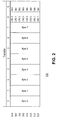
- FIG. 2 illustrates selected aspects of a x8 write frame with data mask and cyclic redundancy code bits, according to an embodiment of the invention.
- Write data frame 200 illustrates a frame of data being written to memory.
- CRC is enabled and frame 200 is a partial write frame (e.g., it includes data mask bits).
- the first eight UI convey write data (e.g., U10 through U17).
- Unit interval 8 conveys the CRC bits (e.g., a CRC byte in the illustrated embodiment).
- the CRC byte covers the data bytes (U10 through U17) as well as the data mask byte (e.g., U19).
- Unit interval 9 conveys the data mask bits that determine which data bytes are masked.
- each data mask bit determines whether the data byte with the corresponding number is masked (e.g., DM0 indicates whether byte 0 is masked, DM1 indicates whether byte 1 is masked, etc.).
- Table 1 lists the associations between data mask bits and write data bytes according to some embodiments of the invention. In alternative embodiments, the associations between data mask bits and write data bytes (or bits, nibbles, etc.) may be different.
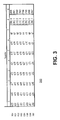
- FIG. 3 illustrates a more detailed bit mapping of a x8 frame according to an embodiment of the invention.
- frame 300 conveys data bits in the first eight UI (UI0 through UI7). It also conveys CRC bits in UI 8 and data mask bits in UI 9.
- the data bits in frame 300 are mapped in a serpentine pattern across the columns of frame 300 to increase the effectives of the coverage provided by the CRC bits. For example, in UI7 the bit at the bottom of the column (in lane DQ7) is q7. The next bit in the sequence, q8, is located at the bottom of the column defined by UI6. The bit at the top of the same column is q15. The next bit in the sequence, q16, is located at the top of the column defined by UI5. This pattern is repeated across the columns of frame 300.
- the generator polynomial for the 8 bit CRC is x ⁇ 8+x ⁇ 5+x ⁇ 3+x ⁇ 2+x+1. In binary, this polynomial may be represented as 0b0 10010111.
- the host e.g., host 110, shown in FIG. 1
- the first stage of the algorithm places the data mask bits into the most significant bits (MSB's) of the write data frame. These bits can be zeroed.
- the data may be placed into the remaining bit locations (e.g., the least significant bits) which are not zeroed.
- a different algorithm may be used.
- the DRAM receives the code word (e.g., Q[71:0]) generated by the host.
- the DRAM checks for an error in the received code word using an appropriate functional equivalent to the following algorithm:
- the first stage (step #3) generates a "local checksum" based on the received code word.
- the local checksum is compared with the received checksum (e.g., the checksum generated at step #2). If an error is detected, the DRAM may provide an error signal to the host (e.g. step #5).
- a different algorithm may be used.
- the XOR equations may be expressed as follows.
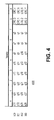
- FIG. 4 illustrates selected aspects of a x4 frame with cyclic redundancy code bits, according to an embodiment of the invention.
- Frame 400 conveys data bits in the first eight U1 (U10 through U17). ). It also conveys CRC bits in U18 and UI 9.
- frame 400 does not include data mask bits because, in many cases, x4 devices do not support data masking as they are primarily used in servers that have error correction code (ECC) and perform a "read-modify-write" operation.
- ECC error correction code
- the data bits in frame 400 are mapped in a serpentine pattern across the columns of frame 400 to increase the effectives of the coverage provided by the CRC bits.
- FIG. 5 is a block diagram illustrating selected aspects of a write data path for a host implemented according to an embodiment of the invention.
- Host 500 includes, inter alia , core logic 502, CRC generator 504, and transmit (TX) framing unit 506.
- host 500 includes more elements, fewer elements, and/or different elements.
- Core logic 502 includes, for example, scheduling logic to schedule reads and writes to main memory as well as retry logic to retry operations when a transmission error occurs.
- core logic 502 includes logic to generate data mask bits 508 to mask at least some of the corresponding write data bits 510.
- core logic 502 schedules, for example, a partial write operation and provides the write data (510) and the corresponding data mask bits (508) to TX framing unit 506 and to CRC generator 504.
- CRC generator 504 generates a CRC checksum based on the write data and the data mask bits.
- a wide array of CRC algorithms may be employed including, for example, an algorithm in which six levels of XOR trees are used to compute the CRC checksum. In alternative embodiments, a different number of XOR trees or a different algorithm may be used to generate the CRC checksum.
- the write data path and the read data path use the same XOR trees to generate the CRC checksum.
- TX framing unit 506 frames the write data (510), the data mask bits (508) and the corresponding CRC checksum into one or more write data frames (e.g., write data frame 512).
- TX framing unit 506 is capable of generating different frame types depending on factors such as whether CRC is enabled and the width of the DRAM.
- TX framing unit 506 may be capable of generating a first frame type which includes a CRC8, 64 data bits, and 8 data mask bits (e.g., for a x8 device).
- TX framing unit 506 may also be capable of generating a second frame type having a CRC8 and 64 data bits (e.g., for a x8 device).
- host 500 may support a third frame type having a CRC8 over 32 bits. In alternative embodiments, more frame types, fewer frame types, and/or different frame types may be supported.
- the write data frame(s) (512) is transferred to one or more memory devices (e.g., DRAMs) via the DQ bus.
- FIG. 6 is a block diagram illustrating selected aspects of a read data path for a memory device implemented according to an embodiment of the invention.
- Memory device 600 includes, inter alia , memory array 602, transmit (TX) framing unit 604, CRC generator 606, and CRC disable logic 608.
- TX transmit
- CRC generator 606 CRC disable logic 608.
- memory device 600 may include more elements, fewer elements, and/or different elements.
- memory device 600 is a dynamic random access memory device (DRAM).
- DRAM dynamic random access memory device
- memory device 600 receives a read command from the host (e.g., host 110) on a C/A bus (e.g., C/A bus 102).
- the data is read from memory array 602 and provided to TX framing unit 604.
- the read data is also provided to CRC generator 606 which computes a CRC checksum.
- CRC generator 606 which computes a CRC checksum.
- six levels of XOR trees are used to compute the CRC checksum.
- a different number of XOR trees or a different algorithm may be used to generate the CRC checksum.
- the read data path and the write data path use the same XOR trees to generate the CRC checksum.
- TX framing unit 604 receives the read data bits and the checksum bits and frames them in a write data frame.
- TX framing unit 604 is capable of using different frame types depending, for example, on whether CRC is enabled.
- TX framing unit 604 may use a first frame type if CRC is enabled and a second frame type if CRC is disabled.
- the first frame type may include both read data bits and a corresponding CRC checksum.
- the second frame type may include the read data bits without the CRC checksum.
- Memory device 600 may transfer the read data frames (with or without a CRC checksum) to the host via DQ bus 610.
- Memory device 600 includes CRC disable logic 608.
- CRC disable logic 608 disables the use of a CRC by memory device 600.
- memory device 600 can be configured to use a CRC checksum with read data or configured to not use a CRC checksum with read data (and/or with write data).
- CRC disable logic includes a portion of a mode register set (MRS).
- FIG. 7 is a flow diagram illustrating selected aspects of a method for transferring data and data mask bits in a common frame with a shared error bit checksum, according to an embodiment of the invention.
- a host e.g., a memory controller
- an error bit checksum e.g., a CRC checksum
- the host includes a CRC generator to generate the CRC checksum. The host may use the same CRC tree for the read data path and the write data path.
- the host (using, e.g., transmit framing unit 506, shown in FIG. 5 ) frames the plurality of data bits into one or more data frames.
- the host can generate different frame types depending on whether CRC is enabled and/or whether a partial write or a full write is being performed.
- the one or more data frames are transferred to a memory device (e.g., a DRAM) via a data bus at 706.
- the DRAM uses the CRC checksum included in the frame provided by the host to determine whether a transmission error has occurred. For example, the DRAM may generate a "local" CRC checksum (based on the received data) and compare the local checksum with the received checksum. If a transmission error has occurred, the DRAM may send an error signal to the host. Referring to decision block 708, if the host receives an error signal, then it may resend the data (at 710). Alternatively, if the host does not receive an error signal, then the data may be valid (at 712).
- Elements of embodiments of the present invention may also be provided as a machine-readable medium for storing the machine-executable instructions.
- the machine-readable medium may include, but is not limited to, flash memory, optical disks, compact disks-read only memory (CD-ROM), digital versatile/video disks (DVD) ROM, random access memory (RAM), erasable programmable read-only memory (EPROM), electrically erasable programmable read-only memory (EEPROM), magnetic or optical cards, propagation media or other type of machine-readable media suitable for storing electronic instructions.
- embodiments of the invention may be downloaded as a computer program which may be transferred from a remote computer (e.g., a server) to a requesting computer (e.g., a client) by way of data signals embodied in a carrier wave or other propagation medium via a communication link (e.g., a modem or network connection).
- a remote computer e.g., a server
- a requesting computer e.g., a client
- a communication link e.g., a modem or network connection
- logic is representative of hardware, firmware, software (or any combination thereof) to perform one or more functions.
- examples of “hardware” include, but are not limited to, an integrated circuit, a finite state machine, or even combinatorial logic.
- the integrated circuit may take the form of a processor such as a microprocessor, an application specific integrated circuit, a digital signal processor, a micro-controller, or the like.
Landscapes
- Engineering & Computer Science (AREA)
- Theoretical Computer Science (AREA)
- General Engineering & Computer Science (AREA)
- Quality & Reliability (AREA)
- Physics & Mathematics (AREA)
- General Physics & Mathematics (AREA)
- Computer Security & Cryptography (AREA)
- Detection And Correction Of Errors (AREA)
- For Increasing The Reliability Of Semiconductor Memories (AREA)
- Techniques For Improving Reliability Of Storages (AREA)
- Memory System (AREA)
- Detection And Prevention Of Errors In Transmission (AREA)
Abstract
Description
- Embodiments of the invention generally relate to the field of integrated circuits and, more particularly, to systems, methods and apparatuses to transfer data and data mask bits in a common frame with a shared error bit code.
- Memory systems may use a partial write command to indicate that at least some of the transferred data is to be masked. The conventional approach to implementing partial writes includes the use of a dedicated data mask pin. For example, a system may include a dedicated data mask pin for each byte lane of data. Thus, a x 16 wide device typically includes two dedicated data mask pins. The data mask pins are typically toggled at the same frequency as the data signals. In many cases, x4 devices do not support data masking because they are primarily used in servers that have error correction code (ECC) and perform a "read-modify-write" operation.
- In addition, the rate at which information is transferred in memory systems continues to increase. These faster transfer rates dictate the use of mechanisms for improved error coverage. Conventional approaches to improving error coverage involve adding pins to the channel. In modem memory systems, the dynamic random memory access (DRAM) channel is pin constrained. Thus, conventional approaches to improving error coverage are not suitable for modem memory systems.
- Embodiments of the invention are illustrated by way of example, and not by way of limitation, in the figures of the accompanying drawings in which like reference numerals refer to similar elements.
-
Figure 1 is a high-level block diagram illustrating selected aspects of a computing system implemented according to an embodiment of the invention. -
Figure 2 illustrates selected aspects of a x8 write frame with data mask bits and cyclic redundancy code bits, according to an embodiment of the invention. -
Figure 3 illustrates a more detailed bit mapping of a x8 frame according to an embodiment of the invention. -
Figure 4 illustrates selected aspects of a x4 frame with cyclic redundancy code bits, according to an embodiment of the invention. -
Figure 5 is a block diagram illustrating selected aspects of a write data path for a host implemented according to an embodiment of the invention. -
Figure 6 is a block diagram illustrating selected aspects of a read data path for a memory device implemented according to an embodiment of the invention. -
Figure 7 is a flow diagram illustrating selected aspects of a method for transferring data and data mask bits in a common frame with a shared error bit checksum, according to an embodiment of the invention. - Embodiments of the invention are generally directed to systems, methods, and apparatuses to transfer data and data mask bits in a common frame with a shared error bit code. A memory system uses data frames to transfer data between a host and a memory device. In some cases, the system may also transfer one or more data mask bits in a data frame (rather than via a separate bit lane). In some embodiments, the system generates an error bit checksum (such as a cyclic redundancy code or CRC) to cover the data bits and the data mask bits. As is further described below, in some embodiments, the data bits, data mask bits, and checksum bits are transferred in a common frame.
- Embodiments of the invention are described below in which CRC is used to provide error coverage for transmission errors. It is to be appreciated, however, that in alternative embodiments a different error bit mechanism may be used. For example, in alternative embodiments, parity bits, error correction code, and the like may be used to provide coverage for transmission errors. The term "error bit" (e.g., a CRC bit) refers to a bit that provides error coverage for one or more data bits.
-
FIG. 1 is a high-level block diagram illustrating selected aspects of a computing system implemented according to an embodiment of the invention. In the illustrated embodiment,system 100 includes host 110 (e.g., a memory controller) and memory device 120 (e.g., a DRAM). In alternative embodiments,system 100 may include more elements, fewer elements, and/or different elements. - Interconnect 101
links host 110 with memory device 120. In some embodiments,interconnect 101 is (at least partly) a point to point interconnect. In other embodiments,interconnect 101 is (at least partly) a multi-drop bus. In some embodiments,interconnect 101 complies, at least in part, with one or more of the standards and/or specifications that define the double data rate bus (e.g., DDR1, DDR2, DDR3, DDR4, and the like). In the illustrated embodiment,interconnect 101 includes command/address lanes 102 and data (or DQ)lanes 104. In other embodiments,interconnect 101 may include more elements, fewer elements, and/or different elements. - Command/Address (C/A)
lanes 102 provide a plurality of lanes for sending commands and addresses to memory device 120.DQ lanes 104 provide a bi-directional read/write data bus. In alternative embodiments,DQ lanes 104 may be unidirectional. For ease of description, embodiments of the invention are described with reference to a x8 memory device. It is to be appreciated, however, that embodiments of the invention may include other device data widths such as x4, x16, x32, etc. -
Host 110 controls the transfer of data to and from memory device 120. In some embodiments,host 110 is integrated onto the same die as one or more processors. In other embodiments,host 110 is part of a computing system's chipset.Host 110 may use a variety of commands to control the transfer of data. For example, the command encoding for a full write may be defined as "W." In some embodiments,host 110 supports a command for partial writes (e.g., Wm). A partial write refers to a write operation in which at least some of the write data is masked using one or more data mask bits. In some embodiments, the data mask bits are transferred in the same frame as the corresponding data bits. -
Host 110 includes, inter alia,CRC logic 112,framing logic 114, and enable/disablelogic 116.CRC logic 112 enableshost 110 to support an in-band CRC mechanism. For example,CRC logic 112 enableshost 110 to generate a CRC checksum that is transferred in one or more data frames (e.g., over DQ lanes 104). In some embodiments, a CRC checksum may be generated for partial write frames. The CRC checksum may cover (at least some of) the data bits and (at least some of) the data mask bits in the write frame. In some embodiments, the data bits, data mask bits, and corresponding checksum are transferred in a common frame (e.g., over DQ lanes 104). - In some embodiments, the use of CRC to cover data frames can be selectively enabled or disabled. For example, in the illustrated embodiment,
host 110 includes enable/disablelogic 116 to selectively enable or disable the use of CRC. In some embodiments, enable/disablelogic 116 may include one or more register bits (e.g., mode register set or MRS bits). -
Host 110 may also includeframing logic 114.Framing logic 114 includes logic to assemble the frames that are transferred to memory device 120. Similarly,logic 114 may also include logic to disassemble the frames that are received from memory device 120. In some embodiments, framinglogic 114 is capable of assembling more than one type of data frame (e.g. data frames 106A, 106B, and 106C). Table 1 illustrates three example frame types according to some embodiments of the invention. It is to be appreciated that in alternative embodiments, other frame types may be used.TABLE 1 Frame Type Description Example Use 1 CRC8 over 72 bits x8 for 64 data bits + 8 mask bits 2 CRC8 over 64 bits x8 for 64 data bits 3 CRC8 over 32 bits x4 for 32 data bits - Memory device 120 provides (at least in part) the main system memory for
system 100. In some embodiments, memory device 120 is a DRAM device (e.g., DDR1, DDR2, DDR3, DDR4, etc.). Memory device 120 includesCRC logic 122, framinglogic 124, and enable disablelogic 126. In some embodiments,CRC logic 122 enables memory device 120 to support an in-band CRC mechanism (e.g., on DQ lines 104). The term "in-band CRC mechanism" refers to supporting CRC (or other error bit scheme) without adding additional pins.CRC logic 122 may include CRC generation logic to generate a local checksum based on a received data frame. The local checksum may be compared with the checksum conveyed in the frame to determine whether there are any transmission errors. Memory device 120 may signalhost 110 when transmission errors occur. -
Framing logic 124 includes logic to assemble the frames that are transferred fromhost 110.Logic 124 may also include logic to disassemble the frames that are received fromhost 110. In some embodiments, framinglogic 124 is capable of assembling more than one type of data frame (e.g. data frames 106). - In some embodiments, the use of CRC to cover data frames can be selectively enabled or disabled. For example, in the illustrated embodiment, memory device 120 includes enable/disable
logic 126 to selectively enable or disable the use of CRC. In some embodiments, enable/disablelogic 126 may include one or more register bits (e.g., mode register set or MRS bits). -
FIG. 2 illustrates selected aspects of a x8 write frame with data mask and cyclic redundancy code bits, according to an embodiment of the invention. Writedata frame 200 illustrates a frame of data being written to memory. In the illustrated embodiment, CRC is enabled andframe 200 is a partial write frame (e.g., it includes data mask bits). The first eight UI convey write data (e.g., U10 through U17).Unit interval 8 conveys the CRC bits (e.g., a CRC byte in the illustrated embodiment). In some embodiments, the CRC byte covers the data bytes (U10 through U17) as well as the data mask byte (e.g., U19).Unit interval 9 conveys the data mask bits that determine which data bytes are masked. In some embodiments, each data mask bit determines whether the data byte with the corresponding number is masked (e.g., DM0 indicates whetherbyte 0 is masked, DM1 indicates whetherbyte 1 is masked, etc.). Table 1 lists the associations between data mask bits and write data bytes according to some embodiments of the invention. In alternative embodiments, the associations between data mask bits and write data bytes (or bits, nibbles, etc.) may be different.TABLE 2 Data Mask Bit Byte Covered by the Data Mask Bit DM0 Byte 0 DM1 Byte 1 DM2 Byte 2 DM3 Byte 3 DM4 Byte 4 DM5 Byte 5 DM6 Byte 6 DM7 Byte 7 -
FIG. 3 illustrates a more detailed bit mapping of a x8 frame according to an embodiment of the invention. Likeframe 200,frame 300 conveys data bits in the first eight UI (UI0 through UI7). It also conveys CRC bits inUI 8 and data mask bits inUI 9. The data bits inframe 300 are mapped in a serpentine pattern across the columns offrame 300 to increase the effectives of the coverage provided by the CRC bits. For example, in UI7 the bit at the bottom of the column (in lane DQ7) is q7. The next bit in the sequence, q8, is located at the bottom of the column defined by UI6. The bit at the top of the same column is q15. The next bit in the sequence, q16, is located at the top of the column defined by UI5. This pattern is repeated across the columns offrame 300. - In some embodiments, the generator polynomial for the 8 bit CRC is x^8+x^5+x^3+x^2+x+1. In binary, this polynomial may be represented as 0b0 10010111. In some embodiments, the host (e.g.,
host 110, shown inFIG. 1 ) may generate a CRC checksum and may form the write data frames using an appropriate functional equivalent for the following algorithm (e.g., for frames that include data mask bits): - 1) Set Q[71 :0]= {DM[7:0]. q[63:0]}
- 2) Set CRC[7:0]= the remainder when Q[71:0] is divided by 0b0 10010111.
- The first stage of the algorithm, places the data mask bits into the most significant bits (MSB's) of the write data frame. These bits can be zeroed. The data may be placed into the remaining bit locations (e.g., the least significant bits) which are not zeroed. In alternative embodiments, a different algorithm may be used.
- The DRAM receives the code word (e.g., Q[71:0]) generated by the host. In some embodiments, the DRAM checks for an error in the received code word using an appropriate functional equivalent to the following algorithm:
- 3) Set R[7:0] = the remainder when Q[71:0] is divided by 0b0 10010111.
- 4) If R[7:0] ≠ CRC[7:0] the received code word contains one or more errors.
- 5) Error reported using an ERROR signal from DRAM.
- The first stage (step #3) generates a "local checksum" based on the received code word. The local checksum is compared with the received checksum (e.g., the checksum generated at step #2). If an error is detected, the DRAM may provide an error signal to the host (e.g. step #5). In alternative embodiments, a different algorithm may be used.
- In some embodiments, CRC XOR equations based on the generator polynomial x^8+x^S+x^3+x^2+x+1 are as follows: 0x97 p(x) = (x+1)(x^7+x^6+x^5+x^2+1). In VHDL equation format with D(71) and CRC(7) being the most significant bits, the XOR equations may be expressed as follows.
- CRC (0) :=
- D(70) xor D(69) xor D(67) xor D(64) xor D(63) xor D(61) xor D(59) xor D(58) xor D(54) xor D(53) xor D(51) xor D(50) xor D(49) xor D(46) xor D(45) xor D(44) xor D(42) xor D(38) xor D(37) xor D(36) xor D(35) xor D(33) xor D(32) xor D(31) xor D(30) xor D(27) xor D(25) xor D(24) xor D(23) xor D(22) xor 0(21) xor D(15) xor D(12) xor D(11) xor D(10) xor D(9) xor D(8) xor D(7) xor D(5) xor D(3) xor D(0) ;
- CRC (1) :=
- D(71) xor D(69) xor D(68) xor D(67) xor D(65) xor D(63) xor D(62) xor D(61) xor D(60) xor D(58) xor D(55) xor D(53) xor D(52) xor D(49) xor D(47) xor D(44) xor D(43) xor D(42) xor D(39) xor D(35) xor D(34) xor D(30) xor D(28) xor D(27) xor D(26) xor D(21) xor D(16) xor D(15) xor D(13) xor D(7) xor D(6) xor D(5) xor D(4) xor D(3) xor D(1) xor D(0) ;
- CRC (2) :=
- D(68) xor D(67) xor D(66) xor D(62) xor D(58) xor D(56) xor D(51) xor D(49) xor D(48) xor D(46) xor D(43) xor D(42) xor D(40) xor D(38) xor D(37) xor D(33) xor D(32) xor D(30) xor D(29) xor D(28) xor D(25) xor D(24) xor D(23) xor D(21) xor D(17) xor D(16) xor D(15) xor D(14) xor D(12) xor D(11) xor D(10) xor D(9) xor D(6) xor D(4) xor D(3) xor D(2) xor D(1) xor D(0);
- CRC (3) :=
- D(70) xor D(68) xor D(64) xor D(61) xor D(58) xor D(57) xor D(54) xor D(53) xor D(52) xor D(51) xor D(47) xor D(46) xor D(45) xor D(43) xor D(42) xor D(41) xor D(39) xor D(37) xor D(36) xor D(35) xor D(34) xor D(32) xor D(29) xor D(27) xor D(26) xor D(23) xor D(21) xor D(18) xor D(17) xor D(16) xor D(13) xor D(9) xor D(8) xor D(4) xor D(2) xor D(1) xor D(0) ;
- CRC (4) :=
- D(71) xor D(69) xor D(65) xor D(62) xor D(59) xor D(58) xor D(55) xor D(54) xor D(53) xor D(52) xor D(48) xor D(47) xor D(46) xor D(44) xor D(43) xor D(42) xor D(40) xor D(38) xor D(37) xor D(36) xor D(35) xor D(33) xor D(30) xor D(28) xor D(27) xor D(24) xor D(22) xor D(19) xor D(18) xor D(17) xor D(14) xor D(10) xor D(9) xor D(5) xor D(3) xor D(2) xor D(1) ;
- CRC (5) :=
- D(69) xor D(67) xor D(66) xor D(64) xor D(61) xor D(60) xor D(58) xor D(56) xor D(55) xor D(51) xor D(50) xor D(48) xor D(47) xor D(46) xor D(43) xor D(42) xor D(41) xor D(39) xor D(35) xor D(34) xor D(33) xor D(32) xor D(30) xor D(29) xor D(28) xor D(27) xor D(24) xor D(22) xor D(21) xor D(20) xor D(19) xor D(18) xor D(12) xor D(9) xor D(8) xor D(7) xor D(6) xor D(5) xor D(4) xor D(2) xor D(0) ;
- CRC (6) :=
- D(70) xor D(68) xor D(67) xor D(65) xor D(62) xor D(61) xor D(59) xor D(57) xor D(56) xor D(52) xor D(51) xor D(49) xor D(48) xor D(47) xor D(44) xor D(43) xor D(42) xor D(40) xor D(36) xor D(35) xor D(34) xor D(33) xor D(31) xor D(30) xor D(29) xor D(28) xor D(25) xor D(23) xor D(22) xor D(21) xor D(20) xor D(19) xor D(13) xor D(10) xor D(9) xor D(8) xor D(7) xor D(6) xor D(5) xor D(3) xor D(1) ;
- CRC (7) :=
- D(71) xor D(69) xor D(68) xor D(66) xor D(63) xor D(62) xor D(60) xor D(58) xor D(57) xor D(53) xor D(52) xor D(50) xor D(49) xor D(48) xor D(45) xor D(44) xor D(43) xor D(41) xor D(37) xor D(36) xor D(35) xor D(34) xor D(32) xor D(31) xor D(30) xor D(29) xor D(26) xor D(24) xor D(23) xor D(22) xor D(21) xor D(20) xor D(14) xor D(11) xor D(10) xor D(9) xor D(8) xor D(7) xor D(6) xor D(4) xor D(2) ;
-
FIG. 4 illustrates selected aspects of a x4 frame with cyclic redundancy code bits, according to an embodiment of the invention.Frame 400 conveys data bits in the first eight U1 (U10 through U17). ). It also conveys CRC bits in U18 andUI 9. In the illustrated embodiment,frame 400 does not include data mask bits because, in many cases, x4 devices do not support data masking as they are primarily used in servers that have error correction code (ECC) and perform a "read-modify-write" operation. The data bits inframe 400 are mapped in a serpentine pattern across the columns offrame 400 to increase the effectives of the coverage provided by the CRC bits. -
FIG. 5 is a block diagram illustrating selected aspects of a write data path for a host implemented according to an embodiment of the invention.Host 500 includes, inter alia,core logic 502,CRC generator 504, and transmit (TX)framing unit 506. In alternative embodiments,host 500 includes more elements, fewer elements, and/or different elements.Core logic 502 includes, for example, scheduling logic to schedule reads and writes to main memory as well as retry logic to retry operations when a transmission error occurs. In addition,core logic 502 includes logic to generate data maskbits 508 to mask at least some of the correspondingwrite data bits 510. - In operation,
core logic 502 schedules, for example, a partial write operation and provides the write data (510) and the corresponding data mask bits (508) toTX framing unit 506 and toCRC generator 504. In some embodiments,CRC generator 504 generates a CRC checksum based on the write data and the data mask bits. A wide array of CRC algorithms may be employed including, for example, an algorithm in which six levels of XOR trees are used to compute the CRC checksum. In alternative embodiments, a different number of XOR trees or a different algorithm may be used to generate the CRC checksum. In some embodiments, the write data path and the read data path use the same XOR trees to generate the CRC checksum. -
TX framing unit 506 frames the write data (510), the data mask bits (508) and the corresponding CRC checksum into one or more write data frames (e.g., write data frame 512). In some embodiments,TX framing unit 506 is capable of generating different frame types depending on factors such as whether CRC is enabled and the width of the DRAM. For example,TX framing unit 506 may be capable of generating a first frame type which includes a CRC8, 64 data bits, and 8 data mask bits (e.g., for a x8 device).TX framing unit 506 may also be capable of generating a second frame type having a CRC8 and 64 data bits (e.g., for a x8 device). Ifhost 500 is coupled with a x4 device, then it may support a third frame type having a CRC8 over 32 bits. In alternative embodiments, more frame types, fewer frame types, and/or different frame types may be supported. The write data frame(s) (512) is transferred to one or more memory devices (e.g., DRAMs) via the DQ bus. -
FIG. 6 is a block diagram illustrating selected aspects of a read data path for a memory device implemented according to an embodiment of the invention.Memory device 600 includes, inter alia,memory array 602, transmit (TX)framing unit 604,CRC generator 606, and CRC disablelogic 608. In alternative embodiments,memory device 600 may include more elements, fewer elements, and/or different elements. In some embodiments,memory device 600 is a dynamic random access memory device (DRAM). - In operation,
memory device 600 receives a read command from the host (e.g., host 110) on a C/A bus (e.g., C/A bus 102). The data is read frommemory array 602 and provided toTX framing unit 604. The read data is also provided toCRC generator 606 which computes a CRC checksum. In some embodiments, six levels of XOR trees are used to compute the CRC checksum. In alternative embodiments, a different number of XOR trees or a different algorithm may be used to generate the CRC checksum. In some embodiments, the read data path and the write data path use the same XOR trees to generate the CRC checksum. -
TX framing unit 604 receives the read data bits and the checksum bits and frames them in a write data frame. In some embodiments,TX framing unit 604 is capable of using different frame types depending, for example, on whether CRC is enabled. For example,TX framing unit 604 may use a first frame type if CRC is enabled and a second frame type if CRC is disabled. The first frame type may include both read data bits and a corresponding CRC checksum. The second frame type may include the read data bits without the CRC checksum.Memory device 600 may transfer the read data frames (with or without a CRC checksum) to the host viaDQ bus 610. -
Memory device 600 includes CRC disablelogic 608. In some embodiments, CRC disablelogic 608 disables the use of a CRC bymemory device 600. Thus, in some embodiments,memory device 600 can be configured to use a CRC checksum with read data or configured to not use a CRC checksum with read data (and/or with write data). In some embodiments, CRC disable logic includes a portion of a mode register set (MRS). -
FIG. 7 is a flow diagram illustrating selected aspects of a method for transferring data and data mask bits in a common frame with a shared error bit checksum, according to an embodiment of the invention. Referring to process block 702, a host (e.g., a memory controller) generates an error bit checksum (e.g., a CRC checksum) to cover transmission errors for a plurality of data bits and to cover (e.g., for a partial write operation) one or more data mask bits. In some embodiments, the host includes a CRC generator to generate the CRC checksum. The host may use the same CRC tree for the read data path and the write data path. - Referring to process block 704, the host (using, e.g., transmit framing
unit 506, shown inFIG. 5 ) frames the plurality of data bits into one or more data frames. In some embodiments, the host can generate different frame types depending on whether CRC is enabled and/or whether a partial write or a full write is being performed. The one or more data frames are transferred to a memory device (e.g., a DRAM) via a data bus at 706. - In some embodiments, the DRAM uses the CRC checksum included in the frame provided by the host to determine whether a transmission error has occurred. For example, the DRAM may generate a "local" CRC checksum (based on the received data) and compare the local checksum with the received checksum. If a transmission error has occurred, the DRAM may send an error signal to the host. Referring to decision block 708, if the host receives an error signal, then it may resend the data (at 710). Alternatively, if the host does not receive an error signal, then the data may be valid (at 712).
- Elements of embodiments of the present invention may also be provided as a machine-readable medium for storing the machine-executable instructions. The machine-readable medium may include, but is not limited to, flash memory, optical disks, compact disks-read only memory (CD-ROM), digital versatile/video disks (DVD) ROM, random access memory (RAM), erasable programmable read-only memory (EPROM), electrically erasable programmable read-only memory (EEPROM), magnetic or optical cards, propagation media or other type of machine-readable media suitable for storing electronic instructions. For example, embodiments of the invention may be downloaded as a computer program which may be transferred from a remote computer (e.g., a server) to a requesting computer (e.g., a client) by way of data signals embodied in a carrier wave or other propagation medium via a communication link (e.g., a modem or network connection).
- In the description above, certain terminology is used to describe embodiments of the invention. For example, the term "logic" is representative of hardware, firmware, software (or any combination thereof) to perform one or more functions. For instance, examples of "hardware" include, but are not limited to, an integrated circuit, a finite state machine, or even combinatorial logic. The integrated circuit may take the form of a processor such as a microprocessor, an application specific integrated circuit, a digital signal processor, a micro-controller, or the like.
- It should be appreciated that reference throughout this specification to "one embodiment" or "an embodiment" means that a particular feature, structure or characteristic described in connection with the embodiment is included in at least one embodiment of the present invention. Therefore, it is emphasized and should be appreciated that two or more references to "an embodiment" or "one embodiment" or "an alternative embodiment" in various portions of this specification are not necessarily all referring to the same embodiment. Furthermore, the particular features, structures or characteristics may be combined as suitable in one or more embodiments of the invention.
- Similarly, it should be appreciated that in the foregoing description of embodiments of the invention, various features are sometimes grouped together in a single embodiment, figure, or description thereof for the purpose of streamlining the disclosure aiding in the understanding of one or more of the various inventive aspects. This method of disclosure, however, is not to be interpreted as reflecting an intention that the claimed subject matter requires more features than are expressly recited in each claim. Rather, as the following claims reflect, inventive aspects lie in less than all features of a single foregoing disclosed embodiment. Thus, the claims following the detailed description are hereby expressly incorporated into this detailed description.
Claims (15)
- An integrated circuit comprising:logic to indicate whether error bit coverage is enabled for a frame to be transferred from the integrated circuit to a memory device;error bit generation logic to generate an error bit checksum to cover the frame, if error bit coverage is enabled; andframing logic to generate the frame, wherein the framing logic is capable of generating the frame based on a number of different frame types, including a first frame type, the first frame type having a plurality of data bits, a plurality of data mask bits, and a corresponding error bit checksum.
- The integrated circuit of claim 1, wherein the frame is based on the first frame type.
- The integrated circuit of claim 2, wherein the data mask bits, DM, are located in the most significant bit locations of the frame (Q).
- The integrated circuit of claim 3, wherein the error bit logic generates a checksum, C, based, at least in part, on dividing Q by a cyclic redundancy code (CRC) generator polynomial.
- The integrated circuit of claim 4, wherein C includes the remainder when Q is divided by the CRC generator polynomial.
- The integrated circuit of claim 5, wherein the CRC generator polynomial is represented in binary by the expression 0b0 10010111.
- The integrated circuit of claim 6, wherein the frame is to be transferred to a x8 dynamic random access memory (DRAM) device and Q is based, at least in part, on the following expression: Q[71:0] = {DM[7:0]. q[63:0]}.
- The integrated circuit of claim 7, wherein C is the remainder when Q[71:0] is divided by 0b0 10010111.
- The integrated circuit of claim 1, wherein the framing logic is capable of generating the frame based on a second frame type, the second frame type including a plurality of data bits and a corresponding error bit checksum.
- The integrated circuit of claim 9, wherein the frame is based on the second frame type and the memory device is a x4 dynamic random access memory (DRAM) device.
- The integrated circuit of claim 10, wherein bits [71:32] of the frame, Q, are set to zero.
- The integrated circuit of claim 11, wherein the checksum, C, is the remainder when Q[71:0] is divided by 0b0 10010111.
- A system comprising:a host, the host includinglogic to indicate whether cyclic redundancy code (CRC) coverage is enabled for a frame to be transferred from the host to a dynamic random access memory (DRAM) device,CRC generation logic to generate a CRC checksum to cover the frame, if CRC coverage is enabled, andframing logic to generate the frame, wherein the framing logic is capable of generating the frame based on a number of different frame types, including a first frame type, the first frame type having a plurality of data bits, a plurality of data mask bits, and a corresponding CRC checksum; andthe DRAM device coupled with the host.
- The system of claim 13, wherein the DRAM device includes
CRC generation logic to generate a local CRC checksum based, at least in part, on dividing the frame by a CRC generator polynomial;
comparison logic to compare the local CRC checksum with the CRC checksum; and
error reporting logic to provide an error indication, if the local CRC checksum does not match the CRC checksum. - The system of claim 14, wherein the frame is based on the first frame type.
Applications Claiming Priority (1)
| Application Number | Priority Date | Filing Date | Title |
|---|---|---|---|
| US12/141,339 US8196009B2 (en) | 2008-06-18 | 2008-06-18 | Systems, methods, and apparatuses to transfer data and data mask bits in a common frame with a shared error bit code |
Publications (2)
| Publication Number | Publication Date |
|---|---|
| EP2136295A1 true EP2136295A1 (en) | 2009-12-23 |
| EP2136295B1 EP2136295B1 (en) | 2012-04-25 |
Family
ID=40957974
Family Applications (1)
| Application Number | Title | Priority Date | Filing Date |
|---|---|---|---|
| EP09251583A Not-in-force EP2136295B1 (en) | 2008-06-18 | 2009-06-17 | Systems, methods, and apparatuses to transfer data and data mask bits in a common frame with a shared error bit code |
Country Status (6)
| Country | Link |
|---|---|
| US (1) | US8196009B2 (en) |
| EP (1) | EP2136295B1 (en) |
| JP (2) | JP2010003299A (en) |
| KR (1) | KR101093857B1 (en) |
| CN (1) | CN101609418B (en) |
| AT (1) | ATE555439T1 (en) |
Cited By (3)
| Publication number | Priority date | Publication date | Assignee | Title |
|---|---|---|---|---|
| WO2013006387A2 (en) | 2011-07-01 | 2013-01-10 | Intel Corporation | Rank-specific cyclic redundancy check |
| EP2652619A4 (en) * | 2010-12-06 | 2014-04-02 | Intel Corp | Memory device on the fly crc mode |
| GB2543877A (en) * | 2015-10-27 | 2017-05-03 | Cirrus Logic Int Semiconductor Ltd | Transfer of data with check bits |
Families Citing this family (20)
| Publication number | Priority date | Publication date | Assignee | Title |
|---|---|---|---|---|
| US8347199B2 (en) * | 2009-01-21 | 2013-01-01 | Cisco Technology, Inc. | Enhanced error detection in multilink serdes channels |
| US8612828B2 (en) * | 2009-12-22 | 2013-12-17 | Intel Corporation | Error correction mechanisms for 8-bit memory devices |
| KR101688051B1 (en) * | 2010-11-08 | 2016-12-20 | 삼성전자 주식회사 | Data processing device and method using error detection code, method for compensating data skew and semiconductor device having data processing device |
| WO2013147733A1 (en) | 2012-03-26 | 2013-10-03 | Intel Corporation | Timing optimization for memory devices employing error detection coded transactions |
| US9299400B2 (en) | 2012-09-28 | 2016-03-29 | Intel Corporation | Distributed row hammer tracking |
| CN103187104B (en) * | 2013-03-19 | 2016-11-23 | 西安紫光国芯半导体有限公司 | The error correction method of DRAM memory |
| US9081700B2 (en) * | 2013-05-16 | 2015-07-14 | Western Digital Technologies, Inc. | High performance read-modify-write system providing line-rate merging of dataframe segments in hardware |
| JP2014225309A (en) | 2013-05-16 | 2014-12-04 | ピーエスフォー ルクスコ エスエイアールエルPS4 Luxco S.a.r.l. | Semiconductor device |
| US9135984B2 (en) * | 2013-12-18 | 2015-09-15 | Micron Technology, Inc. | Apparatuses and methods for writing masked data to a buffer |
| US9354818B2 (en) | 2014-02-25 | 2016-05-31 | Kabushiki Kaisha Toshiba | Memory device and data storing method |
| US9983925B2 (en) * | 2014-04-11 | 2018-05-29 | Micron Technology, Inc. | Apparatuses and methods for fixing a logic level of an internal signal line |
| DE102015209196A1 (en) * | 2014-09-08 | 2016-03-10 | Robert Bosch Gmbh | Method for the serial transmission of a frame via a bus system from a transmitter to at least one receiver and subscribers of a bus system |
| CN107924369B (en) * | 2015-09-11 | 2021-08-31 | 东芝存储器株式会社 | memory device |
| EP3392778A4 (en) * | 2015-12-16 | 2019-01-09 | Sony Corporation | COMMUNICATION DEVICE, COMMUNICATION METHOD, PROGRAM, AND COMMUNICATION SYSTEM |
| US9996414B2 (en) * | 2016-07-12 | 2018-06-12 | International Business Machines Corporation | Auto-disabling DRAM error checking on threshold |
| KR102810613B1 (en) * | 2016-12-02 | 2025-05-21 | 삼성전자주식회사 | error detection code generator of a semiconductor device, a memory controller including the same and a semiconductor memory device including the same |
| WO2019047788A1 (en) | 2017-09-08 | 2019-03-14 | 华为技术有限公司 | Coding method and device |
| CN115378546A (en) * | 2017-09-08 | 2022-11-22 | 华为技术有限公司 | Encoding and decoding method and device |
| US11994943B2 (en) * | 2018-12-31 | 2024-05-28 | Lodestar Licensing Group Llc | Configurable data path for memory modules |
| US11314589B2 (en) * | 2020-05-15 | 2022-04-26 | Intel Corporation | Read retry to selectively disable on-die ECC |
Citations (4)
| Publication number | Priority date | Publication date | Assignee | Title |
|---|---|---|---|---|
| US20030156465A1 (en) | 2002-02-21 | 2003-08-21 | Laberge Paul A. | System and method for multiplexing data and data masking information on a data bus of a memory device |
| WO2006122932A1 (en) | 2005-05-17 | 2006-11-23 | International Business Machines Corporation | Method to handle write mask in dram memory |
| US20070061671A1 (en) | 2005-08-30 | 2007-03-15 | Paul Wallner | Data memory system and method for transferring data into a data memory |
| WO2008005781A2 (en) | 2006-06-30 | 2008-01-10 | Intel Corporation | Improving reliability, availability, and serviceability in a memory device |
Family Cites Families (6)
| Publication number | Priority date | Publication date | Assignee | Title |
|---|---|---|---|---|
| US7272703B2 (en) * | 1997-08-01 | 2007-09-18 | Micron Technology, Inc. | Program controlled embedded-DRAM-DSP architecture and methods |
| JPH1165943A (en) * | 1997-08-21 | 1999-03-09 | Hitachi Ltd | Data transfer device |
| DE102005040109B4 (en) * | 2005-08-24 | 2007-12-27 | Qimonda Ag | Semiconductor memory chip |
| US7734985B2 (en) * | 2006-02-27 | 2010-06-08 | Intel Corporation | Systems, methods, and apparatuses for using the same memory type to support an error check mode and a non-error check mode |
| US7757064B2 (en) * | 2006-09-07 | 2010-07-13 | Infineon Technologies Ag | Method and apparatus for sending data from a memory |
| KR101308047B1 (en) * | 2007-02-08 | 2013-09-12 | 삼성전자주식회사 | Memory system, memory for the same, and command decoding method of the memory |
-
2008
- 2008-06-18 US US12/141,339 patent/US8196009B2/en not_active Expired - Fee Related
-
2009
- 2009-06-16 JP JP2009142981A patent/JP2010003299A/en active Pending
- 2009-06-17 EP EP09251583A patent/EP2136295B1/en not_active Not-in-force
- 2009-06-17 CN CN200910146302.9A patent/CN101609418B/en not_active Expired - Fee Related
- 2009-06-17 AT AT09251583T patent/ATE555439T1/en active
- 2009-06-18 KR KR1020090054352A patent/KR101093857B1/en not_active Expired - Fee Related
-
2012
- 2012-12-11 JP JP2012270332A patent/JP5437470B2/en not_active Expired - Fee Related
Patent Citations (4)
| Publication number | Priority date | Publication date | Assignee | Title |
|---|---|---|---|---|
| US20030156465A1 (en) | 2002-02-21 | 2003-08-21 | Laberge Paul A. | System and method for multiplexing data and data masking information on a data bus of a memory device |
| WO2006122932A1 (en) | 2005-05-17 | 2006-11-23 | International Business Machines Corporation | Method to handle write mask in dram memory |
| US20070061671A1 (en) | 2005-08-30 | 2007-03-15 | Paul Wallner | Data memory system and method for transferring data into a data memory |
| WO2008005781A2 (en) | 2006-06-30 | 2008-01-10 | Intel Corporation | Improving reliability, availability, and serviceability in a memory device |
Cited By (5)
| Publication number | Priority date | Publication date | Assignee | Title |
|---|---|---|---|---|
| EP2652619A4 (en) * | 2010-12-06 | 2014-04-02 | Intel Corp | Memory device on the fly crc mode |
| WO2013006387A2 (en) | 2011-07-01 | 2013-01-10 | Intel Corporation | Rank-specific cyclic redundancy check |
| EP2727115A4 (en) * | 2011-07-01 | 2015-02-18 | Intel Corp | Rank-specific cyclic redundancy check |
| KR101570622B1 (en) | 2011-07-01 | 2015-11-19 | 인텔 코포레이션 | Rank-specific cyclic redundancy check |
| GB2543877A (en) * | 2015-10-27 | 2017-05-03 | Cirrus Logic Int Semiconductor Ltd | Transfer of data with check bits |
Also Published As
| Publication number | Publication date |
|---|---|
| JP2013065347A (en) | 2013-04-11 |
| CN101609418B (en) | 2016-01-20 |
| JP5437470B2 (en) | 2014-03-12 |
| JP2010003299A (en) | 2010-01-07 |
| KR101093857B1 (en) | 2011-12-13 |
| EP2136295B1 (en) | 2012-04-25 |
| ATE555439T1 (en) | 2012-05-15 |
| KR20090131667A (en) | 2009-12-29 |
| CN101609418A (en) | 2009-12-23 |
| US8196009B2 (en) | 2012-06-05 |
| US20090319877A1 (en) | 2009-12-24 |
Similar Documents
| Publication | Publication Date | Title |
|---|---|---|
| EP2136295A1 (en) | Systems, methods, and apparatuses to transfer data and data mask bits in a common frame with a shared error bit code | |
| EP2068245B1 (en) | Reliability, availability, and serviceability solutions for memory technology | |
| JP5135348B2 (en) | Improving memory device reliability, availability, and serviceability | |
| EP1989712B1 (en) | Systems, methods, and apparatuses for using the same memory type to support an error check mode and a non-error check mode | |
| EP2266116B1 (en) | Systems, methods, and apparatuses to save memory self-refresh power | |
| EP2324478B1 (en) | Systems, methods, and apparatuses for in-band data mask bit transmission | |
| US6493843B1 (en) | Chipkill for a low end server or workstation | |
| US20160134307A1 (en) | Completely utilizing hamming distance for secded based ecc dimms | |
| CN116244108A (en) | Memory controller and memory data writing and reading method and storage system | |
| JP2004246754A (en) | Semiconductor memory and its controller | |
| US7836380B2 (en) | Destination indication to aid in posted write buffer loading |
Legal Events
| Date | Code | Title | Description |
|---|---|---|---|
| PUAI | Public reference made under article 153(3) epc to a published international application that has entered the european phase |
Free format text: ORIGINAL CODE: 0009012 |
|
| 17P | Request for examination filed |
Effective date: 20090629 |
|
| AK | Designated contracting states |
Kind code of ref document: A1 Designated state(s): AT BE BG CH CY CZ DE DK EE ES FI FR GB GR HR HU IE IS IT LI LT LU LV MC MK MT NL NO PL PT RO SE SI SK TR |
|
| GRAP | Despatch of communication of intention to grant a patent |
Free format text: ORIGINAL CODE: EPIDOSNIGR1 |
|
| GRAS | Grant fee paid |
Free format text: ORIGINAL CODE: EPIDOSNIGR3 |
|
| GRAA | (expected) grant |
Free format text: ORIGINAL CODE: 0009210 |
|
| AK | Designated contracting states |
Kind code of ref document: B1 Designated state(s): AT BE BG CH CY CZ DE DK EE ES FI FR GB GR HR HU IE IS IT LI LT LU LV MC MK MT NL NO PL PT RO SE SI SK TR |
|
| REG | Reference to a national code |
Ref country code: GB Ref legal event code: FG4D |
|
| REG | Reference to a national code |
Ref country code: CH Ref legal event code: EP |
|
| REG | Reference to a national code |
Ref country code: AT Ref legal event code: REF Ref document number: 555439 Country of ref document: AT Kind code of ref document: T Effective date: 20120515 |
|
| REG | Reference to a national code |
Ref country code: IE Ref legal event code: FG4D |
|
| REG | Reference to a national code |
Ref country code: DE Ref legal event code: R096 Ref document number: 602009006515 Country of ref document: DE Effective date: 20120621 |
|
| REG | Reference to a national code |
Ref country code: NL Ref legal event code: T3 |
|
| REG | Reference to a national code |
Ref country code: AT Ref legal event code: MK05 Ref document number: 555439 Country of ref document: AT Kind code of ref document: T Effective date: 20120425 |
|
| LTIE | Lt: invalidation of european patent or patent extension |
Effective date: 20120425 |
|
| PG25 | Lapsed in a contracting state [announced via postgrant information from national office to epo] |
Ref country code: FI Free format text: LAPSE BECAUSE OF FAILURE TO SUBMIT A TRANSLATION OF THE DESCRIPTION OR TO PAY THE FEE WITHIN THE PRESCRIBED TIME-LIMIT Effective date: 20120425 Ref country code: NO Free format text: LAPSE BECAUSE OF FAILURE TO SUBMIT A TRANSLATION OF THE DESCRIPTION OR TO PAY THE FEE WITHIN THE PRESCRIBED TIME-LIMIT Effective date: 20120725 Ref country code: SE Free format text: LAPSE BECAUSE OF FAILURE TO SUBMIT A TRANSLATION OF THE DESCRIPTION OR TO PAY THE FEE WITHIN THE PRESCRIBED TIME-LIMIT Effective date: 20120425 Ref country code: CY Free format text: LAPSE BECAUSE OF FAILURE TO SUBMIT A TRANSLATION OF THE DESCRIPTION OR TO PAY THE FEE WITHIN THE PRESCRIBED TIME-LIMIT Effective date: 20120425 Ref country code: IS Free format text: LAPSE BECAUSE OF FAILURE TO SUBMIT A TRANSLATION OF THE DESCRIPTION OR TO PAY THE FEE WITHIN THE PRESCRIBED TIME-LIMIT Effective date: 20120825 Ref country code: LT Free format text: LAPSE BECAUSE OF FAILURE TO SUBMIT A TRANSLATION OF THE DESCRIPTION OR TO PAY THE FEE WITHIN THE PRESCRIBED TIME-LIMIT Effective date: 20120425 Ref country code: PL Free format text: LAPSE BECAUSE OF FAILURE TO SUBMIT A TRANSLATION OF THE DESCRIPTION OR TO PAY THE FEE WITHIN THE PRESCRIBED TIME-LIMIT Effective date: 20120425 |
|
| PG25 | Lapsed in a contracting state [announced via postgrant information from national office to epo] |
Ref country code: HR Free format text: LAPSE BECAUSE OF FAILURE TO SUBMIT A TRANSLATION OF THE DESCRIPTION OR TO PAY THE FEE WITHIN THE PRESCRIBED TIME-LIMIT Effective date: 20120425 Ref country code: GR Free format text: LAPSE BECAUSE OF FAILURE TO SUBMIT A TRANSLATION OF THE DESCRIPTION OR TO PAY THE FEE WITHIN THE PRESCRIBED TIME-LIMIT Effective date: 20120726 Ref country code: SI Free format text: LAPSE BECAUSE OF FAILURE TO SUBMIT A TRANSLATION OF THE DESCRIPTION OR TO PAY THE FEE WITHIN THE PRESCRIBED TIME-LIMIT Effective date: 20120425 Ref country code: PT Free format text: LAPSE BECAUSE OF FAILURE TO SUBMIT A TRANSLATION OF THE DESCRIPTION OR TO PAY THE FEE WITHIN THE PRESCRIBED TIME-LIMIT Effective date: 20120827 Ref country code: LV Free format text: LAPSE BECAUSE OF FAILURE TO SUBMIT A TRANSLATION OF THE DESCRIPTION OR TO PAY THE FEE WITHIN THE PRESCRIBED TIME-LIMIT Effective date: 20120425 |
|
| PG25 | Lapsed in a contracting state [announced via postgrant information from national office to epo] |
Ref country code: BE Free format text: LAPSE BECAUSE OF FAILURE TO SUBMIT A TRANSLATION OF THE DESCRIPTION OR TO PAY THE FEE WITHIN THE PRESCRIBED TIME-LIMIT Effective date: 20120425 |
|
| PG25 | Lapsed in a contracting state [announced via postgrant information from national office to epo] |
Ref country code: DK Free format text: LAPSE BECAUSE OF FAILURE TO SUBMIT A TRANSLATION OF THE DESCRIPTION OR TO PAY THE FEE WITHIN THE PRESCRIBED TIME-LIMIT Effective date: 20120425 Ref country code: AT Free format text: LAPSE BECAUSE OF FAILURE TO SUBMIT A TRANSLATION OF THE DESCRIPTION OR TO PAY THE FEE WITHIN THE PRESCRIBED TIME-LIMIT Effective date: 20120425 Ref country code: MC Free format text: LAPSE BECAUSE OF NON-PAYMENT OF DUE FEES Effective date: 20120630 Ref country code: CZ Free format text: LAPSE BECAUSE OF FAILURE TO SUBMIT A TRANSLATION OF THE DESCRIPTION OR TO PAY THE FEE WITHIN THE PRESCRIBED TIME-LIMIT Effective date: 20120425 Ref country code: RO Free format text: LAPSE BECAUSE OF FAILURE TO SUBMIT A TRANSLATION OF THE DESCRIPTION OR TO PAY THE FEE WITHIN THE PRESCRIBED TIME-LIMIT Effective date: 20120425 Ref country code: EE Free format text: LAPSE BECAUSE OF FAILURE TO SUBMIT A TRANSLATION OF THE DESCRIPTION OR TO PAY THE FEE WITHIN THE PRESCRIBED TIME-LIMIT Effective date: 20120425 Ref country code: SK Free format text: LAPSE BECAUSE OF FAILURE TO SUBMIT A TRANSLATION OF THE DESCRIPTION OR TO PAY THE FEE WITHIN THE PRESCRIBED TIME-LIMIT Effective date: 20120425 |
|
| PG25 | Lapsed in a contracting state [announced via postgrant information from national office to epo] |
Ref country code: IT Free format text: LAPSE BECAUSE OF FAILURE TO SUBMIT A TRANSLATION OF THE DESCRIPTION OR TO PAY THE FEE WITHIN THE PRESCRIBED TIME-LIMIT Effective date: 20120425 Ref country code: MK Free format text: LAPSE BECAUSE OF FAILURE TO SUBMIT A TRANSLATION OF THE DESCRIPTION OR TO PAY THE FEE WITHIN THE PRESCRIBED TIME-LIMIT Effective date: 20120425 |
|
| PLBE | No opposition filed within time limit |
Free format text: ORIGINAL CODE: 0009261 |
|
| STAA | Information on the status of an ep patent application or granted ep patent |
Free format text: STATUS: NO OPPOSITION FILED WITHIN TIME LIMIT |
|
| REG | Reference to a national code |
Ref country code: IE Ref legal event code: MM4A |
|
| REG | Reference to a national code |
Ref country code: FR Ref legal event code: ST Effective date: 20130228 |
|
| 26N | No opposition filed |
Effective date: 20130128 |
|
| PG25 | Lapsed in a contracting state [announced via postgrant information from national office to epo] |
Ref country code: ES Free format text: LAPSE BECAUSE OF FAILURE TO SUBMIT A TRANSLATION OF THE DESCRIPTION OR TO PAY THE FEE WITHIN THE PRESCRIBED TIME-LIMIT Effective date: 20120805 Ref country code: FR Free format text: LAPSE BECAUSE OF NON-PAYMENT OF DUE FEES Effective date: 20120702 Ref country code: IE Free format text: LAPSE BECAUSE OF NON-PAYMENT OF DUE FEES Effective date: 20120617 |
|
| REG | Reference to a national code |
Ref country code: DE Ref legal event code: R097 Ref document number: 602009006515 Country of ref document: DE Effective date: 20130128 |
|
| PG25 | Lapsed in a contracting state [announced via postgrant information from national office to epo] |
Ref country code: BG Free format text: LAPSE BECAUSE OF FAILURE TO SUBMIT A TRANSLATION OF THE DESCRIPTION OR TO PAY THE FEE WITHIN THE PRESCRIBED TIME-LIMIT Effective date: 20120725 Ref country code: MT Free format text: LAPSE BECAUSE OF FAILURE TO SUBMIT A TRANSLATION OF THE DESCRIPTION OR TO PAY THE FEE WITHIN THE PRESCRIBED TIME-LIMIT Effective date: 20120425 |
|
| REG | Reference to a national code |
Ref country code: CH Ref legal event code: PL |
|
| PG25 | Lapsed in a contracting state [announced via postgrant information from national office to epo] |
Ref country code: CH Free format text: LAPSE BECAUSE OF NON-PAYMENT OF DUE FEES Effective date: 20130630 Ref country code: LI Free format text: LAPSE BECAUSE OF NON-PAYMENT OF DUE FEES Effective date: 20130630 Ref country code: TR Free format text: LAPSE BECAUSE OF FAILURE TO SUBMIT A TRANSLATION OF THE DESCRIPTION OR TO PAY THE FEE WITHIN THE PRESCRIBED TIME-LIMIT Effective date: 20120425 |
|
| PG25 | Lapsed in a contracting state [announced via postgrant information from national office to epo] |
Ref country code: LU Free format text: LAPSE BECAUSE OF NON-PAYMENT OF DUE FEES Effective date: 20120617 |
|
| PG25 | Lapsed in a contracting state [announced via postgrant information from national office to epo] |
Ref country code: HU Free format text: LAPSE BECAUSE OF FAILURE TO SUBMIT A TRANSLATION OF THE DESCRIPTION OR TO PAY THE FEE WITHIN THE PRESCRIBED TIME-LIMIT Effective date: 20090617 |
|
| PGFP | Annual fee paid to national office [announced via postgrant information from national office to epo] |
Ref country code: NL Payment date: 20180613 Year of fee payment: 10 Ref country code: DE Payment date: 20180605 Year of fee payment: 10 |
|
| PGFP | Annual fee paid to national office [announced via postgrant information from national office to epo] |
Ref country code: GB Payment date: 20180613 Year of fee payment: 10 |
|
| REG | Reference to a national code |
Ref country code: DE Ref legal event code: R119 Ref document number: 602009006515 Country of ref document: DE |
|
| REG | Reference to a national code |
Ref country code: NL Ref legal event code: MM Effective date: 20190701 |
|
| GBPC | Gb: european patent ceased through non-payment of renewal fee |
Effective date: 20190617 |
|
| PG25 | Lapsed in a contracting state [announced via postgrant information from national office to epo] |
Ref country code: DE Free format text: LAPSE BECAUSE OF NON-PAYMENT OF DUE FEES Effective date: 20200101 Ref country code: GB Free format text: LAPSE BECAUSE OF NON-PAYMENT OF DUE FEES Effective date: 20190617 Ref country code: NL Free format text: LAPSE BECAUSE OF NON-PAYMENT OF DUE FEES Effective date: 20190701 |