EP2131493A1 - Acoustic wave branching filter - Google Patents
Acoustic wave branching filter Download PDFInfo
- Publication number
- EP2131493A1 EP2131493A1 EP08751913A EP08751913A EP2131493A1 EP 2131493 A1 EP2131493 A1 EP 2131493A1 EP 08751913 A EP08751913 A EP 08751913A EP 08751913 A EP08751913 A EP 08751913A EP 2131493 A1 EP2131493 A1 EP 2131493A1
- Authority
- EP
- European Patent Office
- Prior art keywords
- acoustic
- wave
- balanced
- longitudinally
- filter
- Prior art date
- Legal status (The legal status is an assumption and is not a legal conclusion. Google has not performed a legal analysis and makes no representation as to the accuracy of the status listed.)
- Withdrawn
Links
Images





Classifications
-
- H—ELECTRICITY
- H03—ELECTRONIC CIRCUITRY
- H03H—IMPEDANCE NETWORKS, e.g. RESONANT CIRCUITS; RESONATORS
- H03H9/00—Networks comprising electromechanical or electro-acoustic elements; Electromechanical resonators
- H03H9/02—Details
- H03H9/05—Holders or supports
- H03H9/0538—Constructional combinations of supports or holders with electromechanical or other electronic elements
- H03H9/0566—Constructional combinations of supports or holders with electromechanical or other electronic elements for duplexers
- H03H9/0576—Constructional combinations of supports or holders with electromechanical or other electronic elements for duplexers including surface acoustic wave [SAW] devices
-
- H—ELECTRICITY
- H03—ELECTRONIC CIRCUITRY
- H03H—IMPEDANCE NETWORKS, e.g. RESONANT CIRCUITS; RESONATORS
- H03H9/00—Networks comprising electromechanical or electro-acoustic elements; Electromechanical resonators
- H03H9/70—Multiple-port networks for connecting several sources or loads, working on different frequencies or frequency bands, to a common load or source
- H03H9/72—Networks using surface acoustic waves
-
- H—ELECTRICITY
- H03—ELECTRONIC CIRCUITRY
- H03H—IMPEDANCE NETWORKS, e.g. RESONANT CIRCUITS; RESONATORS
- H03H9/00—Networks comprising electromechanical or electro-acoustic elements; Electromechanical resonators
- H03H9/0023—Networks for transforming balanced signals into unbalanced signals and vice versa, e.g. baluns, or networks having balanced input and output
- H03H9/0028—Networks for transforming balanced signals into unbalanced signals and vice versa, e.g. baluns, or networks having balanced input and output using surface acoustic wave devices
- H03H9/0047—Networks for transforming balanced signals into unbalanced signals and vice versa, e.g. baluns, or networks having balanced input and output using surface acoustic wave devices having two acoustic tracks
- H03H9/0066—Networks for transforming balanced signals into unbalanced signals and vice versa, e.g. baluns, or networks having balanced input and output using surface acoustic wave devices having two acoustic tracks being electrically parallel
- H03H9/0071—Networks for transforming balanced signals into unbalanced signals and vice versa, e.g. baluns, or networks having balanced input and output using surface acoustic wave devices having two acoustic tracks being electrically parallel the balanced terminals being on the same side of the tracks
-
- H—ELECTRICITY
- H03—ELECTRONIC CIRCUITRY
- H03H—IMPEDANCE NETWORKS, e.g. RESONANT CIRCUITS; RESONATORS
- H03H9/00—Networks comprising electromechanical or electro-acoustic elements; Electromechanical resonators
- H03H9/0023—Networks for transforming balanced signals into unbalanced signals and vice versa, e.g. baluns, or networks having balanced input and output
- H03H9/0028—Networks for transforming balanced signals into unbalanced signals and vice versa, e.g. baluns, or networks having balanced input and output using surface acoustic wave devices
- H03H9/0047—Networks for transforming balanced signals into unbalanced signals and vice versa, e.g. baluns, or networks having balanced input and output using surface acoustic wave devices having two acoustic tracks
- H03H9/0066—Networks for transforming balanced signals into unbalanced signals and vice versa, e.g. baluns, or networks having balanced input and output using surface acoustic wave devices having two acoustic tracks being electrically parallel
- H03H9/0076—Networks for transforming balanced signals into unbalanced signals and vice versa, e.g. baluns, or networks having balanced input and output using surface acoustic wave devices having two acoustic tracks being electrically parallel the balanced terminals being on opposite sides of the tracks
-
- H—ELECTRICITY
- H03—ELECTRONIC CIRCUITRY
- H03H—IMPEDANCE NETWORKS, e.g. RESONANT CIRCUITS; RESONATORS
- H03H9/00—Networks comprising electromechanical or electro-acoustic elements; Electromechanical resonators
- H03H9/02—Details
- H03H9/125—Driving means, e.g. electrodes, coils
- H03H9/145—Driving means, e.g. electrodes, coils for networks using surface acoustic waves
-
- H—ELECTRICITY
- H03—ELECTRONIC CIRCUITRY
- H03H—IMPEDANCE NETWORKS, e.g. RESONANT CIRCUITS; RESONATORS
- H03H9/00—Networks comprising electromechanical or electro-acoustic elements; Electromechanical resonators
- H03H9/25—Constructional features of resonators using surface acoustic waves
-
- H—ELECTRICITY
- H03—ELECTRONIC CIRCUITRY
- H03H—IMPEDANCE NETWORKS, e.g. RESONANT CIRCUITS; RESONATORS
- H03H9/00—Networks comprising electromechanical or electro-acoustic elements; Electromechanical resonators
- H03H9/46—Filters
- H03H9/64—Filters using surface acoustic waves
-
- H—ELECTRICITY
- H03—ELECTRONIC CIRCUITRY
- H03H—IMPEDANCE NETWORKS, e.g. RESONANT CIRCUITS; RESONATORS
- H03H9/00—Networks comprising electromechanical or electro-acoustic elements; Electromechanical resonators
- H03H9/46—Filters
- H03H9/64—Filters using surface acoustic waves
- H03H9/6423—Means for obtaining a particular transfer characteristic
- H03H9/6433—Coupled resonator filters
- H03H9/6436—Coupled resonator filters having one acoustic track only
-
- H—ELECTRICITY
- H03—ELECTRONIC CIRCUITRY
- H03H—IMPEDANCE NETWORKS, e.g. RESONANT CIRCUITS; RESONATORS
- H03H9/00—Networks comprising electromechanical or electro-acoustic elements; Electromechanical resonators
- H03H9/46—Filters
- H03H9/64—Filters using surface acoustic waves
- H03H9/6423—Means for obtaining a particular transfer characteristic
- H03H9/6433—Coupled resonator filters
- H03H9/644—Coupled resonator filters having two acoustic tracks
- H03H9/6456—Coupled resonator filters having two acoustic tracks being electrically coupled
- H03H9/6469—Coupled resonator filters having two acoustic tracks being electrically coupled via two connecting electrodes
- H03H9/6476—Coupled resonator filters having two acoustic tracks being electrically coupled via two connecting electrodes the tracks being electrically parallel
-
- H—ELECTRICITY
- H03—ELECTRONIC CIRCUITRY
- H03H—IMPEDANCE NETWORKS, e.g. RESONANT CIRCUITS; RESONATORS
- H03H9/00—Networks comprising electromechanical or electro-acoustic elements; Electromechanical resonators
- H03H9/46—Filters
- H03H9/64—Filters using surface acoustic waves
- H03H9/6423—Means for obtaining a particular transfer characteristic
- H03H9/6433—Coupled resonator filters
- H03H9/6483—Ladder SAW filters
-
- H—ELECTRICITY
- H03—ELECTRONIC CIRCUITRY
- H03H—IMPEDANCE NETWORKS, e.g. RESONANT CIRCUITS; RESONATORS
- H03H9/00—Networks comprising electromechanical or electro-acoustic elements; Electromechanical resonators
- H03H9/70—Multiple-port networks for connecting several sources or loads, working on different frequencies or frequency bands, to a common load or source
- H03H9/72—Networks using surface acoustic waves
- H03H9/725—Duplexers
-
- H—ELECTRICITY
- H03—ELECTRONIC CIRCUITRY
- H03H—IMPEDANCE NETWORKS, e.g. RESONANT CIRCUITS; RESONATORS
- H03H9/00—Networks comprising electromechanical or electro-acoustic elements; Electromechanical resonators
- H03H9/0023—Networks for transforming balanced signals into unbalanced signals and vice versa, e.g. baluns, or networks having balanced input and output
- H03H9/0028—Networks for transforming balanced signals into unbalanced signals and vice versa, e.g. baluns, or networks having balanced input and output using surface acoustic wave devices
- H03H9/0047—Networks for transforming balanced signals into unbalanced signals and vice versa, e.g. baluns, or networks having balanced input and output using surface acoustic wave devices having two acoustic tracks
- H03H9/0052—Networks for transforming balanced signals into unbalanced signals and vice versa, e.g. baluns, or networks having balanced input and output using surface acoustic wave devices having two acoustic tracks being electrically cascaded
- H03H9/0057—Networks for transforming balanced signals into unbalanced signals and vice versa, e.g. baluns, or networks having balanced input and output using surface acoustic wave devices having two acoustic tracks being electrically cascaded the balanced terminals being on the same side of the tracks
-
- H—ELECTRICITY
- H03—ELECTRONIC CIRCUITRY
- H03H—IMPEDANCE NETWORKS, e.g. RESONANT CIRCUITS; RESONATORS
- H03H9/00—Networks comprising electromechanical or electro-acoustic elements; Electromechanical resonators
- H03H9/0023—Networks for transforming balanced signals into unbalanced signals and vice versa, e.g. baluns, or networks having balanced input and output
- H03H9/0028—Networks for transforming balanced signals into unbalanced signals and vice versa, e.g. baluns, or networks having balanced input and output using surface acoustic wave devices
- H03H9/0047—Networks for transforming balanced signals into unbalanced signals and vice versa, e.g. baluns, or networks having balanced input and output using surface acoustic wave devices having two acoustic tracks
- H03H9/0052—Networks for transforming balanced signals into unbalanced signals and vice versa, e.g. baluns, or networks having balanced input and output using surface acoustic wave devices having two acoustic tracks being electrically cascaded
- H03H9/0061—Networks for transforming balanced signals into unbalanced signals and vice versa, e.g. baluns, or networks having balanced input and output using surface acoustic wave devices having two acoustic tracks being electrically cascaded the balanced terminals being on opposite sides of the tracks
-
- H—ELECTRICITY
- H03—ELECTRONIC CIRCUITRY
- H03H—IMPEDANCE NETWORKS, e.g. RESONANT CIRCUITS; RESONATORS
- H03H9/00—Networks comprising electromechanical or electro-acoustic elements; Electromechanical resonators
- H03H9/0023—Networks for transforming balanced signals into unbalanced signals and vice versa, e.g. baluns, or networks having balanced input and output
- H03H9/0028—Networks for transforming balanced signals into unbalanced signals and vice versa, e.g. baluns, or networks having balanced input and output using surface acoustic wave devices
- H03H9/0085—Networks for transforming balanced signals into unbalanced signals and vice versa, e.g. baluns, or networks having balanced input and output using surface acoustic wave devices having four acoustic tracks
-
- H—ELECTRICITY
- H03—ELECTRONIC CIRCUITRY
- H03H—IMPEDANCE NETWORKS, e.g. RESONANT CIRCUITS; RESONATORS
- H03H9/00—Networks comprising electromechanical or electro-acoustic elements; Electromechanical resonators
- H03H9/46—Filters
- H03H9/64—Filters using surface acoustic waves
- H03H9/6423—Means for obtaining a particular transfer characteristic
- H03H9/6433—Coupled resonator filters
- H03H9/644—Coupled resonator filters having two acoustic tracks
- H03H9/6456—Coupled resonator filters having two acoustic tracks being electrically coupled
- H03H9/6469—Coupled resonator filters having two acoustic tracks being electrically coupled via two connecting electrodes
- H03H9/6473—Coupled resonator filters having two acoustic tracks being electrically coupled via two connecting electrodes the electrodes being electrically interconnected
Definitions
- the present invention relates to a duplexer in which a transmission filter chip and a reception filter chip are mounted on a substrate and, more specifically, to an acoustic-wave duplexer in which each filter chip is made of an acoustic-wave filter chip, such as a surface-acoustic-wave filter chip or a boundary-acoustic-wave filter chip.
- a duplexer that includes a reception filter chip used in a reception circuit and a transmission filter chip used in a transmission circuit.
- Patent Document 1 discloses, as one example of duplexers of this type, a surface-acoustic-wave duplexer illustrated in the diagrammatic circuit diagram in Fig. 17 .
- a transmission acoustic-wave filter chip 1003 and a reception acoustic-wave filter chip 1004 are surface-mounted on a substrate 1002.
- Each of the transmission acoustic-wave filter chip 1003 and the reception acoustic-wave filter chip 1004 has a first end connected to a common terminal 1005.
- the reception acoustic-wave filter chip 1004 is connected to the common terminal 1005 through a phase shift circuit 1006.
- the common terminal 1005 is a terminal connected to an antenna or the like.
- the transmission acoustic-wave filter chip 1003 includes a plurality of series-arm resonators S1 to S3 each made of a 1-port surface-acoustic-wave resonator and parallel-arm resonators P1 and P2 each made of a 1-port surface-acoustic-wave resonator.
- the transmission acoustic-wave filter chip 1003 has an end that is opposite to the first end connected to the common terminal 1005 and that is connected to a transmission terminal 1007.
- An electric signal to be transmitted is input from the transmission terminal 1007 and supplied to the common terminal 1005 through the transmission acoustic-wave filter chip 1003.
- the reception acoustic-wave filter chip 1004 has a structure in which first and second longitudinally-coupled resonator surface-acoustic-wave filters 1008 and 1009 are connected in parallel.
- Each of the longitudinally-coupled resonator surface-acoustic-wave filters 1008 and 1009 includes a first IDT arranged in its center. First ends of the first IDTs are commonly connected to the common terminal 1005 through the phase shift circuit. A second end of each of the first IDTs is connected to a ground potential.
- First ends of second and third IDTs arranged at both sides of the first IDT of the longitudinally-coupled resonator surface-acoustic-wave filter 1008 in a surface wave propagation direction are commonly connected to a first reception terminal 1010.
- First ends of second and third IDTs of the longitudinally-coupled resonator surface-acoustic-wave filter 1009 are also commonly connected to the first reception terminal 1010.
- the second and third IDTs of each of the longitudinally-coupled resonator surface-acoustic-wave filters 1008 and 1009 are commonly connected to a second reception terminal 1011 serving as a second balanced terminal.
- reception acoustic-wave filter chip 1004 is a surface-acoustic-wave filter including the first and second reception terminals 1010 and 1011 and having the balanced-to-unbalanced conversion function.
- the transmission acoustic-wave filter chip 1003 forming the transmission filter and the reception acoustic-wave filter chip 1004 forming the reception filter are surface-mounted on the substrate 1002 to aim at multifunction. Accordingly, the number of parts can be reduced.
- the reception acoustic-wave filter chip 1004 has the balanced-to-unbalanced conversion function, as described above, so a balun can be omitted.
- the transmission acoustic-wave filter chip 1003 has a ladder circuit configuration, and during transmission a transmission current flows and a magnetic field occurs.
- a reception current is conveyed from the first reception terminal 1010 being the first balanced terminal toward the second reception terminal 1011 serving as the second balanced terminal.
- an induced current caused by the above-described magnetic field flows while being superimposed on the reception current. Because of this, a problem is present in which the isolation characteristic in the reception acoustic-wave filter chip 1004 deteriorates in the pass band of the transmission band-pass filter.
- an acoustic-wave duplexer including a substrate, a reception acoustic-wave filter chip, and a transmission acoustic-wave filter chip, the reception and transmission acoustic-wave filters being mounted on the substrate.
- the substrate includes first and second balanced terminals, a common terminal, and a signal terminal.
- Each of the transmission acoustic-wave filter chip and the reception acoustic-wave filter chip includes at least one acoustic-wave excitation electrode, and at least one of the transmission acoustic-wave filter chip and the reception acoustic-wave filter chip is a balanced filter unit that includes, as an input terminal or an output terminal, a first balanced signal terminal and a second balanced signal terminal.
- the acoustic-wave duplexer further includes a first interconnection that connects the balanced filter unit and the first balanced terminal and a second interconnection that connects the balanced filter unit and the second balanced terminal.
- the first balanced signal end of the balanced filter unit is a junction of the balanced filter unit and the first interconnection
- the second balanced signal end thereof is a junction of the balanced filter unit and the second interconnection.
- the first and second interconnections intersect with each other while being insulated from each other.
- the substrate may be provided with a portion where the first and second interconnections intersect with each other.
- the portion where the first and second interconnections intersect with each other while being insulated from each other can be readily formed.
- the substrate may be a laminated substrate in which a plurality of insulating layers are laminated, and the substrate may further include a plurality of conductive patterns spaced by a corresponding insulating layer of the laminated substrate disposed therebetween and a via-hole conductor disposed so as to electrically connect at least two of the plurality of conductive patterns spaced by the corresponding insulating layer of the laminated substrate disposed therebetween.
- the structure in which the first and second interconnections intersect with each other while being insulated from each other can be readily formed by formation of at least one interconnection using one of the above-described conductive patterns.
- the portion where the first and second interconnections intersect with each other may be provided to the balanced filter chip.
- the substrate can have a reduced size.
- the reception acoustic-wave filter chip of the transmission acoustic-wave filter chip and the reception acoustic-wave filter chip may be the balanced filter unit.
- the reception acoustic-wave filter chip is of the balanced type, the necessity of connecting the reception acoustic-wave filter chip with a balun can be obviated.
- the acoustic-wave duplexer can have a reduced size.
- the above-described balanced filter unit can be formed variously.
- the balanced filter unit may include a piezoelectric substrate and first and second longitudinally-coupled resonator acoustic-wave filters provided to the piezoelectric substrate.
- Each of the first and second longitudinally-coupled resonator acoustic-wave filters may include, as the acoustic-wave excitation electrode, a first IDT and second and third IDTs arranged at both sides of the first IDT in an acoustic-wave propagation direction and may further include a pair of reflectors arranged at both side of a region in which the first to third IDTs are disposed in the acoustic-wave propagation direction.
- the second IDTs of the first and second longitudinally-coupled resonator acoustic-wave filters may be connected to each other.
- the third IDTs of the first and second longitudinally-coupled resonator acoustic-wave filters may be connected to each other.
- a first bus bar of the first IDT of the second longitudinally-coupled resonator acoustic-wave filter may be a first balanced signal input/output unit.
- a second bus bar of the first IDT of the second longitudinally-coupled resonator acoustic-wave filter may be a second balanced signal input/output unit.
- This preferable balanced filter unit is hereinafter abbreviated as a particular preferable balanced filter unit.
- the first balanced signal input/output unit may be connected to the first balanced signal end, and the second balanced signal input/output unit may be connected to the second balanced signal end.
- the balanced filter unit may comprise two above-described particular preferable balanced filter units, the two balanced filter units being connected in parallel. Te first balanced signal input/output units of both of the two balanced filter units may be connected to the first balanced signal end. The second balanced signal input/output units of both of the two balanced filter units may be connected to the second balanced signal end.
- the balanced filter unit may comprise two above-described particular balanced filter units provided on the piezoelectric substrate, the two balanced filter units being connected in parallel.
- the first balanced signal input/output units of both of the two balanced filter units may be connected to the first balanced signal end.
- the second balanced signal input/output unit of either one of the two balanced filter units may be connected to the second balanced signal end.
- the balanced filter unit may comprise two above-described particular balanced filter units provided on the piezoelectric substrate, the two balanced filter units being connected in parallel.
- the first balanced signal input/output unit of either one of the two balanced filter units may be connected to the first balanced signal end.
- the second balanced signal input/output units of both of the two balanced filter units may be connected to the second balanced signal end.
- the acoustic-wave duplexer may also have a structure in which the balanced filter unit including a piezoelectric substrate and first and second longitudinally-coupled resonator acoustic-wave filters provided to the piezoelectric substrate, each of the first and second longitudinally-coupled resonator acoustic-wave filters including, as the acoustic-wave excitation electrode, a first IDT and second and third IDTs arranged at both sides of the first IDT in an acoustic-wave propagation direction and further including a pair of reflectors arranged at both side of a region in which the first to third IDTs are disposed in the acoustic-wave propagation direction, the first balanced signal end being a portion of the first IDT or the second and third IDTs of the first longitudinally-coupled resonator acoustic-wave filter, the portion being connected to the first interconnection, the second balanced signal end being a portion of the first IDT or the second and third I
- the acoustic-wave duplexer may also have a structure in which the balanced filter unit includes a piezoelectric substrate and first to fourth longitudinally-coupled resonator acoustic-wave filters provided to the piezoelectric substrate, each of the first to fourth longitudinally-coupled resonator acoustic-wave filters includes, as the acoustic-wave excitation electrode, a first IDT and second and third IDTs arranged at both sides of the first IDT in an acoustic-wave propagation direction, each of the first to fourth longitudinally-coupled resonator acoustic-wave filters further includes a pair of reflectors arranged at both side of a region in which the first to third IDTs are disposed in the acoustic-wave propagation direction, the first and third longitudinally-coupled resonator acoustic-wave filters are cascaded, the second and fourth longitudinally-coupled resonator acoustic-wave filters are cascaded, the second
- the transmission band-pass filter may be made of a ladder acoustic-wave filter. In this case, a small insertion loss can be achieved.
- a surface acoustic wave may be used, and thus a surface-acoustic-wave filter device may be configured.
- a boundary acoustic wave may be used, and thus a boundary-acoustic-wave filter chip may be configured.
- the balanced filter unit may contain a piezoelectric resonator that includes a substrate, a piezoelectric film supported by the substrate and acoustically isolated from the substrate, and an upper electrode film and a lower electrode film as the excitation electrode.
- the upper electrode film and the lower electrode film are disposed such that the piezoelectric film is arranged therebetween.
- the transmission acoustic-wave filter chip and the reception acoustic-wave filter chip are mounted on the substrate, at least one of the transmission acoustic-wave filter chip and the reception acoustic-wave filter chip is the balanced filter unit, and the first interconnection connecting the balanced filter unit and the first balanced terminal and the second interconnection connecting the balanced filter unit and the second balanced terminal intersect with each other while being insulated from each other.
- the isolation characteristic in the pass band of a transmission band-pass filter in the reception acoustic-wave filter chip is improved, and the isolation characteristic in the pass band of a reception band-pass filter in the transmission acoustic-wave filter chip is improved.
- the duplexer in which a reception acoustic-wave filter chip and a transmission acoustic-wave filter chip are surface-mounted on a substrate and at least one of the filter chips is a balanced filter unit, the duplexer being capable of reducing its size, the isolation characteristic between the transmission acoustic-wave filter chip and the reception acoustic-wave filter chip can be effectively improved.
- the size of a mobile communication device such as a cellular phone, can be reduced, and the isolation between transmission and reception sides can also be enhanced. Accordingly, communication performance in transmission and reception can be enhanced.
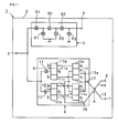
- Fig. 1 is a schematic circuit diagram that illustrates a circuit configuration of a duplexer according to an embodiment of the present invention.
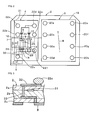
- Fig. 2 is a schematic plan view that illustrates a structure of the duplexer according to the present embodiment
- Fig. 3 is a partially cut-away side cross-sectional view that illustrates a main portion thereof.
- a duplexer 1 includes a substrate 2.
- the substrate 2 is formed from a plurality of insulating layers and also made of a laminated substrate having conductor patterns laminated with the insulating layers disposed therebetween. The structure of the laminated substrate is described later.
- An insulating material forming each of the insulating layers is not limited to a particular one, and as the material, proper insulation ceramic, for example, alumina, and synthetic resin can be used.
- the substrate 2 is provided with a common terminal 5 for use in connecting to an antenna.
- the common terminal 5 is connected to the transmission acoustic-wave filter chip 3.
- the transmission acoustic-wave filter chip 3 is a surface-acoustic-wave filter having a ladder circuit configuration that has three series-arm resonators S1-S3 and three parallel-arm resonators P1-P3.
- Each of the series-arm resonators S1-S3 and the parallel-arm resonators P1-P3 is made of a 1-port surface-acoustic-wave resonator.
- the transmission acoustic-wave filter chip 3 is electrically connected to a transmission terminal 6.
- a transmission signal is input from the transmission terminal 6 and output to the common terminal 5, which is connected to the antenna, through the transmission acoustic-wave filter chip 3.
- the duplexer 1 is used as a duplexer of a cellular phone of PCS system.
- the transmission frequency band is between 1850 and 1910 MHz, and the reception frequency band is between 1930 and 1990 MHz.
- the reception acoustic-wave filter chip 4 has a first end connected to the common terminal 5 and a second end electrically connected to first and second balanced terminals 7 and 8 serving as first and second reception terminals, respectively.
- the reception acoustic-wave filter chip 4 has a circuit configuration illustrated in Fig. 1 . That is, first and second longitudinally-coupled resonator surface-acoustic-wave filters 11 and 12 are connected to the common terminal 5 through 1-port surface-acoustic-wave resonators 9 and 10, respectively. Although being schematically illustrated in Fig. 1 , each of the longitudinally-coupled resonator surface-acoustic-wave filters 11 and 12 is a 3-IDT longitudinally-coupled resonator surface-acoustic-wave filter.
- the first longitudinally-coupled resonator surface-acoustic-wave filter 11 includes a first IDT 11a arranged in the center and second and third IDTs 11b and 11c arranged at both sides of the first IDT 11a in a surface-wave propagation direction.
- the longitudinally-coupled resonator surface-acoustic-wave filter 12 includes first to third IDTs 12a-12c.
- a first end of the first IDT 11a and that of the first IDT 12a in the first and second longitudinally-coupled resonator surface-acoustic-wave filters are commonly connected to the common terminal 5 through the 1-port surface-acoustic-wave resonators 9 and 10, respectively.
- Each of the IDTs 11a and 12a has a second end connected to a ground potential.
- Each of the second and third IDTs 11b and 11c of the first longitudinally-coupled resonator surface-acoustic-wave filter 11 has a first end connected to a ground potential, and second ends thereof are connected to first ends of the second and third IDTs 13b and 13c, respectively, of a 3-IDT longitudinally-coupled resonator surface-acoustic-wave filter 13.
- Each of the IDTs 13b and 13c has a second end connected to a ground potential.
- each of the IDTs 12b and 12c has a first end connected to a ground potential. Second ends of the IDTs 12b and 12c are electrically connected to first ends of IDTs 14b and 14c, respectively. Each of the IDTs 14b and 14c has a second electrode connected to a ground potential. A first end of a first IDT 14a and a first end of a first IDT 13a are commonly connected to the first balanced terminal 7, which serves as the first balanced signal terminal. Second ends of the first IDTs 14a and 13a are also commonly connected to the second balanced terminal 8, which serves as the second reception terminal.
- first and second balanced terminals 7 and 8 are disposed adjacent to the substrate 2.
- the reception surface-acoustic-wave filter chip 4 is electrically connected to the first balanced terminal 7 by a first interconnection 15.
- the reception surface-acoustic-wave filter chip 4 is connected to the second balanced terminal 8 by a second interconnection 16.
- the junction of the first interconnection 15 and the reception surface-acoustic-wave filter chip 4 is a first balanced signal end 17, whereas the junction of the second interconnection 16 and the reception surface-acoustic-wave filter chip 4 is a second balanced signal end 18.
- each of the transmission surface-acoustic-wave filter chip 3 and the reception surface-acoustic-wave filter chip 4 is provided by formation of electrodes and interconnection patterns made of proper metal, such as aluminum, or alloy on a single side of a piezoelectric substrate to implement the above-described circuit configuration.
- the common terminal 5 and the first and second balanced terminals 7 and 8 are provided to the substrate 2. Meanwhile, as illustrated in Fig. 2 , in the present embodiment, the first and second interconnections 15 and 16 are disposed so as to reach onto the substrate 2, on which the reception surface-acoustic-wave filter chip 4 is formed.
- a characteristic of the present embodiment is intersection of the first interconnection 15 and the second interconnection 16 as indicated by the arrow "A" illustrated in Fig. 1 . This makes it possible to improve an isolation characteristic of the transmission surface-acoustic-wave filter chip 3 and the reception surface-acoustic-wave filter chip 4 in their respective pass bands.
- FIG. 1 A specific structure illustrated in Fig. 1 is described with reference to Figs. 2 and 3 .
- Fig. 2 illustrates, using a schematic plan view, the structure in which the transmission surface-acoustic-wave filter chip 3 and the reception surface-acoustic-wave filter chip 4 are mounted on the substrate 2.
- the transmission surface-acoustic-wave filter chip 3 includes a piezoelectric substrate 19.
- An electrode structure and an interconnection pattern for implementing the circuit configuration of the transmission surface-acoustic-wave filter chip 3 illustrated in Fig. 1 are disposed on a lower surface of the piezoelectric substrate 19. Note that, in Fig. 2 , for the sake of simplification of illustration, the piezoelectric substrate 19 is illustrated so as to be seen therethrough and the above-described electrode structure and interconnection patterns are omitted.
- a plurality of bumps 20a to 20h are disposed on the lower surface of the piezoelectric substrate 19 so as to be connected to the interconnection patter on the substrate 2. These bumps 20a to 20h are provided at the lower surface of the piezoelectric substrate 19 so as to project downward.
- the bumps 20a to 20h are electrically connected to corresponding electrodes connected to the common terminal 5, the ground terminals, and the transmission terminal 6 of the transmission surface-acoustic-wave filter chip 3.
- the bump 20a is a bump connected to the common terminal 5
- the bumps 20d to 20g are bumps connected to the ground terminals
- the bump 20h is a bump connected to the transmission terminal 6, which is illustrated in Fig. 1 .
- the bumps 20b and 20c are electrically floating dummy bumps provided to allow the transmission surface-acoustic-wave filter chip 3 to be stably mounted on the substrate 2.
- a transmission current for example, as indicated by the arrow B, flows.
- the transmission current produces a magnetic field.
- a plurality of bumps 22a to 22f are disposed on a lower surface of a piezoelectric substrate 21.
- an electrode structure as schematically indicated by the solid lines in Fig. 1 , is disposed on the lower surface of the piezoelectric substrate 21.
- the bumps 22a to 22f also project downward from the lower surface of the piezoelectric substrate 21.
- the bumps 22a to 22f are electrically connected to corresponding electrodes connected to the common terminal 5, the ground terminals, and the first and second balanced terminals 7 and 8 of the reception surface-acoustic-wave filter chip 4.
- the bump 22a is a floating bump
- the bumps 22b and 22e are bumps connected to the ground terminals
- the bump 22c is a bump connected to the second balanced terminal.
- the bump 22d is a bump connected to the common terminal 5
- the bump 22f is a bump electrically connected to the first balanced terminal.
- an interconnection pattern indicated by the solid lines and an interconnection pattern indicated by the broken lines are disposed at different height positions within the piezoelectric substrate 21.
- the interconnection patterns disposed at different height positions are electrically connected to each other by via-hole conductors 24, 25, and 26.
- the first balanced terminal 7 and the first balanced signal end 17 are connected to each other by the first interconnection 15, and the second balanced terminal 8 and the second balanced signal end 18 are connected to each other by the second interconnection 16 (see Fig. 1 ).
- This is realized onto the substrate 2 illustrated in Fig. 2 in the present embodiment. That is, in Fig. 2 , an interconnection pattern 31 indicated by the alternate long and short dashed lines forms the first interconnection 15, whereas an interconnection pattern 32 indicated by the alternate long and short dashed lines forms the second interconnection 16.
- Fig. 3 shows the partially cut-away side cross-sectional view illustrated in Fig. 3 , which shows the portion taken along the line C-C of Fig.
- the interconnection patterns 31 and 32 are disposed at different height positions in the substrate 2, and accordingly, they intersect with each other while being insulated from each other. More specifically, as illustrated in Fig. 3 , the substrate 2 has a structure in which first and second insulating layers 2a and 2b are laminated.
- the interconnection pattern 32 forming the second interconnection to which the bump 22c disposed on the lower surface of the reception surface-acoustic-wave filter chip 4 is coupled is disposed on the substrate 2.
- the interconnection pattern 32 is electrically connected to the second balanced terminal 8 disposed on the lower surface of the substrate 2 through a via-hole conductor 33.
- the interconnection pattern 31 forming the first interconnection 15 is disposed in the border between the insulating layers 2a and 2b.
- the interconnection pattern 31 has an L shape indicated by the alternate long and short dashed lines at the height position between the insulating layers 2a and 2b.
- the first balanced terminal 7 is disposed on the lower surface of the substrate 2.
- the first balanced terminal 7 and the interconnection pattern 31 are electrically connected to each other by a via-hole electrode (not shown).
- This structure suppresses the effects of a magnetic field produced by the above-described transmission current flowing in the direction indicated by the arrow B and thus improves the isolation characteristic between the surface-acoustic-wave filter chips 3 and 4.
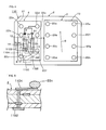
- a duplexer 1101 of this comparative example includes a transmission surface-acoustic-wave filter chip and a reception surface-acoustic-wave filter chip that are substantially the same as those in the above-described embodiment. The only difference is that the first and second interconnections connecting the first and second balanced signal ends of the reception surface-acoustic-wave filter chip with the first and second balanced terminals do not intersect with each other.
- an interconnection pattern 1104 serving as the first interconnection connected to the first balanced signal end and a first balanced terminal 1102 and an interconnection pattern 1105 forming the second interconnection connected to the second balanced signal end and a second balanced terminal 1103 are isolated from each other so as not to intersect with each other, as illustrated.
- the duplexer 1101 of the above-described comparative example has a configuration similar to the duplexer 1 of the above-described embodiment. Accordingly, the description of the common portions is omitted by use of the same reference numerals in the common portions.
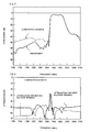
- Fig. 6 shows isolation characteristics of duplexers of the above-described embodiment and comparative example.
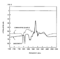
- Fig. 7 illustrates filter characteristics of reception surface-acoustic-wave filters.
- the solid lines represent a result of the above-described embodiment, whereas the broken lines represent a result of the above-described comparative example.
- the vertical axis of Figs. 6 and 7 indicates an attenuation (dB).
- Fig. 6 shows the degree of leakage of signals from the transmission surface-acoustic-wave filter chip 3 toward the reception surface-acoustic-wave filter chip 4.
- Fig. 7 which shows filter characteristics of the reception surface-acoustic-wave filters, it is found that, according to the above-described embodiment, attenuation in the transmission pass-band can be sufficiently increased in comparison with that according to the comparative example.
- intersection of the first and second interconnections can sufficiently improve the isolation characteristic. This is because, in the reception surface-acoustic-wave filter chip 4, which is a balanced filter chip, the characteristic is improved by enhancement in balance.
- an output single in the first balanced terminal and that in the second balanced terminal have the same amplitude and the same phase.
- the differential amplitude approaches 0, and larger attenuation is obtainable. Accordingly, the greater the degree of balance, the greater the characteristic, in comparison with that obtained when the outputs would be unbalanced.
- Figs. 8 and 9 show an amplitude characteristic in isolation in the comparative example and that in the embodiment, respectively.
- the solid lines indicate the amplitude characteristic between the common terminal and the first balanced terminal 7
- the broken lines indicates the amplitude characteristic between the common terminal and the second balanced terminal 8.
- the horizontal axis indicates a frequency
- the vertical axis indicates an attenuation.
- Fig. 10 shows a phase balance characteristic in isolation. That is, Fig. 10 shows a phase difference between a signal output to the first balanced terminal and a signal output to the second balanced terminal when a signal is input into a transmission terminal.
- the vertical axis indicates a phase difference
- the thin line indicates a result of the comparative example
- the thick line indicates a result of the above-described embodiment.
- the isolation in the transmission surface-acoustic-wave filter chip 3 and the reception surface-acoustic-wave filter chip 4 can be effectively enhanced.
- the circuit configuration in the reception surface-acoustic-wave filter chip 4 is not limited to one illustrated in Fig. 1 .
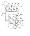
- Circuit configurations of duplexers according to such modification examples in which balanced filter units have modified circuit configurations are illustrated in Figs. 11 to 17 using diagrammatic plan views.
- a reception surface-acoustic-wave filter chip 54 is a balanced surface-acoustic-wave filter chip.
- the first to fourth 3-IDT type longitudinally-coupled resonator surface-acoustic-wave filters 11 to 14 are used.
- the first and second balanced signal ends 17 and 18 connected to the first and second balanced terminals 7 and 8 are connected to first ends of the first IDTs 13a and 14a of the third and fourth longitudinally-coupled resonator surface-acoustic-wave filters, and the second ends of the first IDTs 13a and 14a are connected to ground potentials.
- the reception surface-acoustic-wave filter chip 54 having a two-stage cascaded structure with a neutral point may also be used.
- the first and second interconnections 15 and 16 intersect with each other while being insulated from each other, as illustrated.
- the isolation characteristic is improved by enhancement in balance.
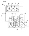
- Fig. 12 is a schematic plan view that illustrates a duplexer according to another modification example of the present invention.
- a reception surface-acoustic-wave filter chip 64 is made of a floating balanced surface-acoustic-wave filter chip.
- the reception surface-acoustic-wave filter chip 64 includes first and second 3-IDT type longitudinally-coupled resonator surface-acoustic-wave filters 62 and 63.
- First ends of central first IDTs 62a and 63a of the first and second longitudinally-coupled resonator surface-acoustic-wave filters 62 and 63 are connected to the common terminal 5 through the 1-port surface-acoustic-wave resonators 9 and 10, respectively. Second ends thereof are connected to ground potentials. First ends of second and third IDTs 62b, 62c, 63b, and 63c are commonly connected to the first balanced signal end 17, and second ends thereof are commonly connected to the second balanced signal end 18.
- the other configuration is substantially the same as that in the first embodiment.
- the first and second interconnections 15 and 16 intersect with each other while being insulated from each other.
- the isolation characteristic is improved by improvement in balance characteristic.
- Fig. 13 is a diagrammatic plan view that illustrates a circuit configuration of a duplexer according to still another modification example of the present invention.
- a duplexer 71 illustrated in Fig. 13 similar to the modification example illustrated in Fig. 12 , the first and second longitudinally-coupled resonator surface-acoustic-wave filters 62 and 63 are connected to the common terminal 5 through the 1-port surface-acoustic-wave resonators 9 and 10, respectively.
- a single-stage structure with a neutral point is used, so the first ends of the second and third IDTs 62b and 62c are commonly connected to the first balanced signal end, and the first ends of second and third IDTs 63b and 63c are commonly connected to the second balanced signal end.
- the second ends of the IDTs 62a to 62c and 63a to 63c are connected to ground potentials.
- a neutral-point type having the two longitudinally-coupled resonator surface-acoustic-wave filters 62 and 63 may also be used. Also in this case, because the first and second interconnections 15 and 16 intersect with each other, the balance is enhanced, and this improves the isolation characteristic.
- Fig. 14 is a schematic circuit diagram that illustrates a duplexer according to still another modification example of the present invention.
- a duplexer 81 illustrated in Fig. 14 the portion where the first and second interconnections 15 and 16 intersect with each other is disposed adjacent to the reception surface-acoustic-wave filter chip 4.
- the other respects are substantially the same as in the first embodiment.
- the portion where the first and second interconnections 15 and 16 intersect with each other may also be disposed within the reception surface-acoustic-wave filter chip 4, i.e., a balanced surface-acoustic-wave filter chip, not on the substrate 2.
- Fig. 15 is a circuit diagram that illustrates still another modification example of the present invention.
- a duplexer 91 according to this modification example similar to the case of the duplexer 81 according to the modification example illustrated in Fig. 14 , the portion where the first and second interconnections 15 and 16 intersect with each other is disposed within the reception surface-acoustic-wave filter chip, which is a balanced filter chip.
- a bus bar of each of the central IDTs 13a and 14a of the third and fourth longitudinally-coupled resonator surface-acoustic-wave filters 13 and 14 are a balanced signal input/output unit.
- a second bus bar (balanced signal input/output unit) of the central IDT 14a is connected to the second balanced signal end 18.
- a second bus bar (balanced signal input/output unit) of the central IDT 13a is connected to the second balanced terminal 8 through another interconnection 116. Similar to the case of the duplexer 81 according to the modification example illustrated in Fig.
- the first bus bar (balanced signal input/output unit) of the central IDT 13a and the first bus bar (balanced signal input/output unit) of the central IDT 14a are both connected to the first balanced signal end 17.
- the first and second balanced signal ends 17 and 18 are connected to first ends of the first and second interconnections 15 and 16, respectively.
- the portion where the first and second interconnections intersect with each other in the balanced filter chip may also be the portion where the first interconnection 15 connected to the two first bus bars and the second interconnection connected to one of the two second bus bars intersect with each other.
- the transmission filter has a ladder circuit configuration, but it is not limited to the one having the ladder circuit configuration.
- At least one of the transmission surface-acoustic-wave filter chip and the reception surface-acoustic-wave filter chip may be a balanced filter chip, so the reception surface-acoustic-wave filter chip does not necessarily have to be of the balanced type.
- boundary-acoustic-wave filter chips making use of a boundary acoustic wave may also be used.
- the above-described balanced filter unit may also be formed using a piezoelectric resonator illustrated in Fig. 16 .
- a piezoelectric resonator 101 illustrated in Fig. 16 includes a substrate 102.
- the substrate 102 is made of proper insulation ceramic or synthetic resin, for example.
- a piezoelectric thin film 103 is disposed on the substrate 102.
- a lower electrode 104 and an upper electrode 105 are disposed so as to be opposed to each other such that the piezoelectric thin film 103 is disposed therebetween.
- Each of the lower electrode 104 and the upper electrode 105 forms an excitation electrode according to the present invention and is made of a proper metal, such as silver or aluminum, or alloy.
- the piezoelectric thin film 103 is made of proper piezoelectric ceramic, such as PZTK ceramic.
- the balanced filter unit may also be formed using the piezoelectric resonator 101 using this piezoelectric thin film 103.
- the angle of intersection of the first and second interconnections 15 and 16 may be 90°.
- the angle is not 90°, a similar advantage of improving isolation is obtainable.
Landscapes
- Physics & Mathematics (AREA)
- Acoustics & Sound (AREA)
- Surface Acoustic Wave Elements And Circuit Networks Thereof (AREA)
Abstract
Description
- The present invention relates to a duplexer in which a transmission filter chip and a reception filter chip are mounted on a substrate and, more specifically, to an acoustic-wave duplexer in which each filter chip is made of an acoustic-wave filter chip, such as a surface-acoustic-wave filter chip or a boundary-acoustic-wave filter chip.
- Traditionally, for a mobile communication system, such as a cellular phone, in order to reduce the number of parts, a composite part having multiple functions is highly desired. As one such example of the composite part, a duplexer is known that includes a reception filter chip used in a reception circuit and a transmission filter chip used in a transmission circuit.
- For example,
Patent Document 1 mentioned below discloses, as one example of duplexers of this type, a surface-acoustic-wave duplexer illustrated in the diagrammatic circuit diagram inFig. 17 . - In a surface-acoustic-wave duplexer 1001, a transmission acoustic-
wave filter chip 1003 and a reception acoustic-wave filter chip 1004 are surface-mounted on asubstrate 1002. Each of the transmission acoustic-wave filter chip 1003 and the reception acoustic-wave filter chip 1004 has a first end connected to acommon terminal 1005. The reception acoustic-wave filter chip 1004 is connected to thecommon terminal 1005 through aphase shift circuit 1006. Thecommon terminal 1005 is a terminal connected to an antenna or the like. - The transmission acoustic-
wave filter chip 1003 includes a plurality of series-arm resonators S1 to S3 each made of a 1-port surface-acoustic-wave resonator and parallel-arm resonators P1 and P2 each made of a 1-port surface-acoustic-wave resonator. The transmission acoustic-wave filter chip 1003 has an end that is opposite to the first end connected to thecommon terminal 1005 and that is connected to atransmission terminal 1007. An electric signal to be transmitted is input from thetransmission terminal 1007 and supplied to thecommon terminal 1005 through the transmission acoustic-wave filter chip 1003. - Meanwhile, the reception acoustic-
wave filter chip 1004 has a structure in which first and second longitudinally-coupled resonator surface-acoustic-wave filters wave filters common terminal 1005 through the phase shift circuit. A second end of each of the first IDTs is connected to a ground potential. - First ends of second and third IDTs arranged at both sides of the first IDT of the longitudinally-coupled resonator surface-acoustic-
wave filter 1008 in a surface wave propagation direction are commonly connected to afirst reception terminal 1010. - First ends of second and third IDTs of the longitudinally-coupled resonator surface-acoustic-
wave filter 1009 are also commonly connected to thefirst reception terminal 1010. The second and third IDTs of each of the longitudinally-coupled resonator surface-acoustic-wave filters second reception terminal 1011 serving as a second balanced terminal. - Accordingly, the above-described reception acoustic-
wave filter chip 1004 is a surface-acoustic-wave filter including the first andsecond reception terminals - [Patent Document 1] Japanese Unexamined Patent Application Publication No.
2003-249832 - For the surface-acoustic-wave duplexer 1001 described in
Patent Document 1, the transmission acoustic-wave filter chip 1003 forming the transmission filter and the reception acoustic-wave filter chip 1004 forming the reception filter are surface-mounted on thesubstrate 1002 to aim at multifunction. Accordingly, the number of parts can be reduced. In addition, the reception acoustic-wave filter chip 1004 has the balanced-to-unbalanced conversion function, as described above, so a balun can be omitted. - However, there is a problem in which isolation between the transmission acoustic-
wave filter chip 1003 and the reception acoustic-wave filter chip 1004 is not sufficient. That is, the transmission acoustic-wave filter chip 1003 has a ladder circuit configuration, and during transmission a transmission current flows and a magnetic field occurs. For the balanced reception acoustic-wave filter chip 1004, a reception current is conveyed from thefirst reception terminal 1010 being the first balanced terminal toward thesecond reception terminal 1011 serving as the second balanced terminal. However, in a transmission frequency band, an induced current caused by the above-described magnetic field flows while being superimposed on the reception current. Because of this, a problem is present in which the isolation characteristic in the reception acoustic-wave filter chip 1004 deteriorates in the pass band of the transmission band-pass filter. - It is an object of the present invention to overcome the above-described drawbacks in the related art and to provide an acoustic-wave duplexer having a configuration in which at least one of a transmission acoustic-wave filter chip and a reception acoustic-wave filter chip is a balanced filter chip and having a satisfactory isolation characteristic between a reception acoustic-wave filter chip and a transmission acoustic-wave filter chip.
- According to the present invention, there is provided an acoustic-wave duplexer including a substrate, a reception acoustic-wave filter chip, and a transmission acoustic-wave filter chip, the reception and transmission acoustic-wave filters being mounted on the substrate. The substrate includes first and second balanced terminals, a common terminal, and a signal terminal. Each of the transmission acoustic-wave filter chip and the reception acoustic-wave filter chip includes at least one acoustic-wave excitation electrode, and at least one of the transmission acoustic-wave filter chip and the reception acoustic-wave filter chip is a balanced filter unit that includes, as an input terminal or an output terminal, a first balanced signal terminal and a second balanced signal terminal. The acoustic-wave duplexer further includes a first interconnection that connects the balanced filter unit and the first balanced terminal and a second interconnection that connects the balanced filter unit and the second balanced terminal. The first balanced signal end of the balanced filter unit is a junction of the balanced filter unit and the first interconnection, and the second balanced signal end thereof is a junction of the balanced filter unit and the second interconnection. The first and second interconnections intersect with each other while being insulated from each other.
- For the acoustic-wave duplexer according to the present invention, preferably, the substrate may be provided with a portion where the first and second interconnections intersect with each other. In this case, the portion where the first and second interconnections intersect with each other while being insulated from each other can be readily formed. In this case, more preferably, the substrate may be a laminated substrate in which a plurality of insulating layers are laminated, and the substrate may further include a plurality of conductive patterns spaced by a corresponding insulating layer of the laminated substrate disposed therebetween and a via-hole conductor disposed so as to electrically connect at least two of the plurality of conductive patterns spaced by the corresponding insulating layer of the laminated substrate disposed therebetween. In this case, because the plurality of conductive patterns spaced by the corresponding insulating layer are provided to the laminated substrate and at least two of the plurality of conductive patterns obtained through the insulating layers are electrically connected to each other using the via hole, the structure in which the first and second interconnections intersect with each other while being insulated from each other can be readily formed by formation of at least one interconnection using one of the above-described conductive patterns.
- For the acoustic-wave duplexer according to the present invention, the portion where the first and second interconnections intersect with each other may be provided to the balanced filter chip. In this case, it is not necessary to provide the structure in which the first and second interconnections intersect with each other while being insulated from each other to the substrate, the substrate can have a reduced size.
- For the acoustic-wave duplexer according to the present invention, preferably, the reception acoustic-wave filter chip of the transmission acoustic-wave filter chip and the reception acoustic-wave filter chip may be the balanced filter unit. In this case, because the reception acoustic-wave filter chip is of the balanced type, the necessity of connecting the reception acoustic-wave filter chip with a balun can be obviated. Thus, the acoustic-wave duplexer can have a reduced size.
- For the acoustic-wave duplexer according to the present invention, the above-described balanced filter unit can be formed variously. Preferably, the balanced filter unit may include a piezoelectric substrate and first and second longitudinally-coupled resonator acoustic-wave filters provided to the piezoelectric substrate. Each of the first and second longitudinally-coupled resonator acoustic-wave filters may include, as the acoustic-wave excitation electrode, a first IDT and second and third IDTs arranged at both sides of the first IDT in an acoustic-wave propagation direction and may further include a pair of reflectors arranged at both side of a region in which the first to third IDTs are disposed in the acoustic-wave propagation direction. The second IDTs of the first and second longitudinally-coupled resonator acoustic-wave filters may be connected to each other. The third IDTs of the first and second longitudinally-coupled resonator acoustic-wave filters may be connected to each other. A first bus bar of the first IDT of the second longitudinally-coupled resonator acoustic-wave filter may be a first balanced signal input/output unit. A second bus bar of the first IDT of the second longitudinally-coupled resonator acoustic-wave filter may be a second balanced signal input/output unit. This preferable balanced filter unit is hereinafter abbreviated as a particular preferable balanced filter unit.
- Preferably, the first balanced signal input/output unit may be connected to the first balanced signal end, and the second balanced signal input/output unit may be connected to the second balanced signal end.
- With a particular aspect of the acoustic-wave duplexer according to the present invention, the balanced filter unit may comprise two above-described particular preferable balanced filter units, the two balanced filter units being connected in parallel. Te first balanced signal input/output units of both of the two balanced filter units may be connected to the first balanced signal end. The second balanced signal input/output units of both of the two balanced filter units may be connected to the second balanced signal end.
- With another particular aspect of the acoustic-wave duplexer according to the present invention, the balanced filter unit may comprise two above-described particular balanced filter units provided on the piezoelectric substrate, the two balanced filter units being connected in parallel. The first balanced signal input/output units of both of the two balanced filter units may be connected to the first balanced signal end. The second balanced signal input/output unit of either one of the two balanced filter units may be connected to the second balanced signal end.
- With still another particular aspect of the acoustic-wave duplexer according to the present invention, the balanced filter unit may comprise two above-described particular balanced filter units provided on the piezoelectric substrate, the two balanced filter units being connected in parallel. The first balanced signal input/output unit of either one of the two balanced filter units may be connected to the first balanced signal end. The second balanced signal input/output units of both of the two balanced filter units may be connected to the second balanced signal end.
- The acoustic-wave duplexer according to the present invention may also have a structure in which the balanced filter unit including a piezoelectric substrate and first and second longitudinally-coupled resonator acoustic-wave filters provided to the piezoelectric substrate, each of the first and second longitudinally-coupled resonator acoustic-wave filters including, as the acoustic-wave excitation electrode, a first IDT and second and third IDTs arranged at both sides of the first IDT in an acoustic-wave propagation direction and further including a pair of reflectors arranged at both side of a region in which the first to third IDTs are disposed in the acoustic-wave propagation direction, the first balanced signal end being a portion of the first IDT or the second and third IDTs of the first longitudinally-coupled resonator acoustic-wave filter, the portion being connected to the first interconnection, the second balanced signal end being a portion of the first IDT or the second and third IDTs of the second longitudinally-coupled resonator acoustic-wave filter, the portion being connected to the second interconnection, a phase of an output signal to an input signal in the second longitudinally-coupled resonator acoustic-wave filter differing by 180° from a phase of an output signal to an input signal in the first longitudinally-coupled resonator acoustic-wave filter.
- The acoustic-wave duplexer according to the present invention may also have a structure in which the balanced filter unit includes a piezoelectric substrate and first to fourth longitudinally-coupled resonator acoustic-wave filters provided to the piezoelectric substrate, each of the first to fourth longitudinally-coupled resonator acoustic-wave filters includes, as the acoustic-wave excitation electrode, a first IDT and second and third IDTs arranged at both sides of the first IDT in an acoustic-wave propagation direction, each of the first to fourth longitudinally-coupled resonator acoustic-wave filters further includes a pair of reflectors arranged at both side of a region in which the first to third IDTs are disposed in the acoustic-wave propagation direction, the first and third longitudinally-coupled resonator acoustic-wave filters are cascaded, the second and fourth longitudinally-coupled resonator acoustic-wave filters are cascaded, the first balanced signal end is a portion of the first IDT or the second and third IDTs of the third longitudinally-coupled resonator acoustic-wave filter, the portion being connected to the first interconnection, the second balanced signal end is a portion of the first IDT or the second and third IDTs of the fourth longitudinally-coupled resonator acoustic-wave filter, the portion being connected to the second interconnection, phases of an output signal to an input signal in three filters of the first to fourth longitudinally-coupled resonator acoustic-wave filters are the same, and the phases differs by 180° from a phase of an output signal to an input signal in the remaining one filter.
- For the acoustic-wave duplexer according to the present invention, the transmission band-pass filter may be made of a ladder acoustic-wave filter. In this case, a small insertion loss can be achieved.
- For the acoustic-wave duplexer according to the present invention, as the acoustic wave, a surface acoustic wave may be used, and thus a surface-acoustic-wave filter device may be configured. Alternatively, a boundary acoustic wave may be used, and thus a boundary-acoustic-wave filter chip may be configured.
- For the acoustic-wave duplexer according to the present invention, preferably, the balanced filter unit may contain a piezoelectric resonator that includes a substrate, a piezoelectric film supported by the substrate and acoustically isolated from the substrate, and an upper electrode film and a lower electrode film as the excitation electrode. The upper electrode film and the lower electrode film are disposed such that the piezoelectric film is arranged therebetween.
- For the acoustic-wave duplexer according to the present invention, the transmission acoustic-wave filter chip and the reception acoustic-wave filter chip are mounted on the substrate, at least one of the transmission acoustic-wave filter chip and the reception acoustic-wave filter chip is the balanced filter unit, and the first interconnection connecting the balanced filter unit and the first balanced terminal and the second interconnection connecting the balanced filter unit and the second balanced terminal intersect with each other while being insulated from each other. Thus, the isolation characteristic in the pass band of a transmission band-pass filter in the reception acoustic-wave filter chip is improved, and the isolation characteristic in the pass band of a reception band-pass filter in the transmission acoustic-wave filter chip is improved.
- Accordingly, for a duplexer in which a reception acoustic-wave filter chip and a transmission acoustic-wave filter chip are surface-mounted on a substrate and at least one of the filter chips is a balanced filter unit, the duplexer being capable of reducing its size, the isolation characteristic between the transmission acoustic-wave filter chip and the reception acoustic-wave filter chip can be effectively improved.
- Accordingly, the size of a mobile communication device, such as a cellular phone, can be reduced, and the isolation between transmission and reception sides can also be enhanced. Accordingly, communication performance in transmission and reception can be enhanced.
-
- [
Fig. 1] Fig. 1 is a diagrammatic circuit diagram that illustrates a circuit configuration of a duplexer according to a first embodiment of the present invention. - [
Fig. 2] Fig. 2 is a plan view that schematically illustrates a duplexer according to an embodiment of the present invention. - [
Fig. 3] Fig. 3 is a partially cut-away enlarged side view that illustrates a portion extending along the line C-C in the duplexer ofFig. 2 . - [
Fig. 4] Fig. 4 is a schematic plan view of a traditional duplexer prepared for comparison. - [
Fig. 5] Fig. 5 is a partially cut-away enlarged side view that illustrates a portion extending along the line D-D in the duplexer prepared for comparison illustrated inFig. 4 . - [
Fig. 6] Fig. 6 is an illustration showing isolation characteristics of the duplexer according to the embodiment and the duplexer according to the comparative example. - [
Fig. 7] Fig. 7 is an illustration showing filter characteristics of the duplexer according to the embodiment and the duplexer according to the comparative example. - [
Fig. 8] Fig. 8 is an illustration showing an amplitude characteristic in an isolation characteristic in the duplexer prepared for comparison. - [
Fig. 9] Fig. 9 is an illustration showing an amplitude characteristic in an isolation characteristic in the embodiment illustrated inFig. 1 . - [
Fig. 10] Fig. 10 is an illustration showing phase balance characteristics in the traditional example prepared for comparison and in the embodiment. - [
Fig. 11] Fig. 11 is a schematic circuit diagram that illustrates a duplexer according to a modification example of the present invention. - [
Fig. 12] Fig. 12 is a schematic circuit diagram that illustrates a duplexer according to another modification example of the present invention. - [
Fig. 13] Fig. 13 is a schematic circuit diagram that illustrates a duplexer according to still another modification example of the present invention. - [
Fig. 14] Fig. 14 is a schematic circuit diagram that illustrates a duplexer according to another modification example of the present invention. - [
Fig. 15] Fig. 15 is a schematic circuit diagram that illustrates a duplexer according to still another modification example of the present invention. - [
Fig. 16] Fig. 16 is a schematic front view that illustrates an example of a piezoelectric resonator forming a balanced filter unit according to the present invention. - [
Fig. 17] Fig. 17 is a schematic circuit diagram that illustrates a circuit configuration of a traditional duplexer. -
- 1: duplexer
- 2: substrate
- 2a, 2b: insulating layers
- 3: transmission surface-acoustic-wave filter chip
- 4: reception surface-acoustic-wave filter chip
- 5: common terminal
- 6: transmission terminal
- 7: first balanced terminal
- 8: second balanced terminal
- 9: 1-port surface-acoustic-wave resonator
- 10: 1-port surface-acoustic-wave resonator
- 11-14: longitudinally-coupled resonator surface-acoustic-wave filters
- 11a-11c: first to third IDTs
- 12a-12c: first to third IDTs
- 13a-13c: first to third IDTs
- 14a-14c: first to third IDTs
- 15: first interconnection
- 16: second interconnection
- 17: first balanced signal end
- 18: second balanced signal end
- 19: piezoelectric substrate
- 20a-20h: bumps
- 21: piezoelectric substrate
- 22a-22f: bumps
- 24, 25, 26: via-hole conductors
- 31, 32: interconnection patterns
- 33: via-hole conductor
- 51: duplexer
- 54: reception surface-acoustic-wave filter chip
- 61: duplexer
- 62, 63: first and second 3-IDT longitudinally-coupled resonator surface-acoustic-wave filters
- 62a-62c: IDTs
- 63a-63c: IDTs
- 64: reception surface-acoustic-wave filter chip
- 71: duplexer
- 81: duplexer
- 91: duplexer
- 101: piezoelectric resonator
- 102: substrate
- 103: piezoelectric thin film
- 104: lower electrode
- 105: upper electrode
- 116: interconnection
- P1-P3: parallel-arm resonators
- S1-S3: series-arm resonators
- The present invention is explained below by the description of specific embodiments of the present invention with reference to the drawings.
-
Fig. 1 is a schematic circuit diagram that illustrates a circuit configuration of a duplexer according to an embodiment of the present invention.Fig. 2 is a schematic plan view that illustrates a structure of the duplexer according to the present embodiment, andFig. 3 is a partially cut-away side cross-sectional view that illustrates a main portion thereof. - A
duplexer 1 according to the present embodiment includes asubstrate 2. With the present embodiment, thesubstrate 2 is formed from a plurality of insulating layers and also made of a laminated substrate having conductor patterns laminated with the insulating layers disposed therebetween. The structure of the laminated substrate is described later. - An insulating material forming each of the insulating layers is not limited to a particular one, and as the material, proper insulation ceramic, for example, alumina, and synthetic resin can be used.
- A transmission surface-acoustic-
wave filter chip 3 and a reception surface-acoustic-wave filter chip 4, each of which has a circuit configuration illustrated inFig. 1 , are mounted on thesubstrate 2. Thesubstrate 2 is provided with acommon terminal 5 for use in connecting to an antenna. Thecommon terminal 5 is connected to the transmission acoustic-wave filter chip 3. The transmission acoustic-wave filter chip 3 is a surface-acoustic-wave filter having a ladder circuit configuration that has three series-arm resonators S1-S3 and three parallel-arm resonators P1-P3. - Each of the series-arm resonators S1-S3 and the parallel-arm resonators P1-P3 is made of a 1-port surface-acoustic-wave resonator.
- The transmission acoustic-
wave filter chip 3 is electrically connected to atransmission terminal 6. A transmission signal is input from thetransmission terminal 6 and output to thecommon terminal 5, which is connected to the antenna, through the transmission acoustic-wave filter chip 3. - The
duplexer 1 according to the present embodiment is used as a duplexer of a cellular phone of PCS system. The transmission frequency band is between 1850 and 1910 MHz, and the reception frequency band is between 1930 and 1990 MHz. - The reception acoustic-
wave filter chip 4 has a first end connected to thecommon terminal 5 and a second end electrically connected to first and secondbalanced terminals - The reception acoustic-
wave filter chip 4 has a circuit configuration illustrated inFig. 1 . That is, first and second longitudinally-coupled resonator surface-acoustic-wave filters common terminal 5 through 1-port surface-acoustic-wave resonators Fig. 1 , each of the longitudinally-coupled resonator surface-acoustic-wave filters wave filter 11 includes a first IDT 11a arranged in the center and second andthird IDTs wave filter 12 includes first tothird IDTs 12a-12c. A first end of the first IDT 11a and that of thefirst IDT 12a in the first and second longitudinally-coupled resonator surface-acoustic-wave filters are commonly connected to thecommon terminal 5 through the 1-port surface-acoustic-wave resonators - Each of the
IDTs 11a and 12a has a second end connected to a ground potential. - Each of the second and
third IDTs wave filter 11 has a first end connected to a ground potential, and second ends thereof are connected to first ends of the second andthird IDTs wave filter 13. Each of theIDTs - Similarly, the downstream stage of the second longitudinally-coupled resonator surface-acoustic-
wave filter 12 is connected to a fourth 3-IDT longitudinally-coupled resonator surface-acoustic-wave filter 14. That is, each of theIDTs IDTs IDTs IDTs first IDT 14a and a first end of a first IDT 13a are commonly connected to the firstbalanced terminal 7, which serves as the first balanced signal terminal. Second ends of thefirst IDTs 14a and 13a are also commonly connected to the secondbalanced terminal 8, which serves as the second reception terminal. - Here, the first and second
balanced terminals substrate 2. The reception surface-acoustic-wave filter chip 4 is electrically connected to the firstbalanced terminal 7 by afirst interconnection 15. Meanwhile, the reception surface-acoustic-wave filter chip 4 is connected to the secondbalanced terminal 8 by asecond interconnection 16. Here, the junction of thefirst interconnection 15 and the reception surface-acoustic-wave filter chip 4 is a firstbalanced signal end 17, whereas the junction of thesecond interconnection 16 and the reception surface-acoustic-wave filter chip 4 is a secondbalanced signal end 18. - It is noted that each of the transmission surface-acoustic-
wave filter chip 3 and the reception surface-acoustic-wave filter chip 4 is provided by formation of electrodes and interconnection patterns made of proper metal, such as aluminum, or alloy on a single side of a piezoelectric substrate to implement the above-described circuit configuration. - It is noted that, in the present embodiment, the
common terminal 5 and the first and secondbalanced terminals substrate 2. Meanwhile, as illustrated inFig. 2 , in the present embodiment, the first andsecond interconnections substrate 2, on which the reception surface-acoustic-wave filter chip 4 is formed. - A characteristic of the present embodiment is intersection of the
first interconnection 15 and thesecond interconnection 16 as indicated by the arrow "A" illustrated inFig. 1 . This makes it possible to improve an isolation characteristic of the transmission surface-acoustic-wave filter chip 3 and the reception surface-acoustic-wave filter chip 4 in their respective pass bands. - A specific structure illustrated in
Fig. 1 is described with reference toFigs. 2 and 3 . -
Fig. 2 illustrates, using a schematic plan view, the structure in which the transmission surface-acoustic-wave filter chip 3 and the reception surface-acoustic-wave filter chip 4 are mounted on thesubstrate 2. Here, the transmission surface-acoustic-wave filter chip 3 includes apiezoelectric substrate 19. An electrode structure and an interconnection pattern for implementing the circuit configuration of the transmission surface-acoustic-wave filter chip 3 illustrated inFig. 1 are disposed on a lower surface of thepiezoelectric substrate 19. Note that, inFig. 2 , for the sake of simplification of illustration, thepiezoelectric substrate 19 is illustrated so as to be seen therethrough and the above-described electrode structure and interconnection patterns are omitted. A plurality of bumps 20a to 20h are disposed on the lower surface of thepiezoelectric substrate 19 so as to be connected to the interconnection patter on thesubstrate 2. These bumps 20a to 20h are provided at the lower surface of thepiezoelectric substrate 19 so as to project downward. The bumps 20a to 20h are electrically connected to corresponding electrodes connected to thecommon terminal 5, the ground terminals, and thetransmission terminal 6 of the transmission surface-acoustic-wave filter chip 3. Here, the bump 20a is a bump connected to thecommon terminal 5; thebumps 20d to 20g are bumps connected to the ground terminals; and thebump 20h is a bump connected to thetransmission terminal 6, which is illustrated inFig. 1 . Thebumps wave filter chip 3 to be stably mounted on thesubstrate 2. For the transmission surface-acoustic-wave filter chip 3, from the side of thebump 20h connected to thetransmission terminal 6 toward the side of the bump 20a connected to the common terminal, a transmission current, for example, as indicated by the arrow B, flows. The transmission current produces a magnetic field. - Meanwhile, as illustrated in
Fig. 2 , also for the reception surface-acoustic-wave filter chip 4, a plurality ofbumps 22a to 22f are disposed on a lower surface of apiezoelectric substrate 21. For the reception surface-acoustic-wave filter chip 4, an electrode structure, as schematically indicated by the solid lines inFig. 1 , is disposed on the lower surface of thepiezoelectric substrate 21. - The
bumps 22a to 22f also project downward from the lower surface of thepiezoelectric substrate 21. Thebumps 22a to 22f are electrically connected to corresponding electrodes connected to thecommon terminal 5, the ground terminals, and the first and secondbalanced terminals wave filter chip 4. - Among the
bumps 22a to 22f, thebump 22a is a floating bump, thebumps bump 22c is a bump connected to the second balanced terminal. Thebump 22d is a bump connected to thecommon terminal 5, and thebump 22f is a bump electrically connected to the first balanced terminal. Thesebumps 22b to 22f are electrically connected to the reception surface-acoustic-wave filter disposed on the lower surface of thepiezoelectric substrate 21. - Among the interconnection patterns connecting the first to fourth longitudinally-coupled resonator surface-acoustic-
wave filters 11 to 14 disposed in the reception surface-acoustic-wave filter chip 4, an interconnection pattern indicated by the solid lines and an interconnection pattern indicated by the broken lines are disposed at different height positions within thepiezoelectric substrate 21. The interconnection patterns disposed at different height positions are electrically connected to each other by via-hole conductors - Meanwhile, in the present embodiment, the first
balanced terminal 7 and the firstbalanced signal end 17 are connected to each other by thefirst interconnection 15, and the secondbalanced terminal 8 and the secondbalanced signal end 18 are connected to each other by the second interconnection 16 (seeFig. 1 ). This is realized onto thesubstrate 2 illustrated inFig. 2 in the present embodiment. That is, inFig. 2 , aninterconnection pattern 31 indicated by the alternate long and short dashed lines forms thefirst interconnection 15, whereas aninterconnection pattern 32 indicated by the alternate long and short dashed lines forms thesecond interconnection 16. As is clear from the partially cut-away side cross-sectional view illustrated inFig. 3 , which shows the portion taken along the line C-C ofFig. 2 , theinterconnection patterns substrate 2, and accordingly, they intersect with each other while being insulated from each other. More specifically, as illustrated inFig. 3 , thesubstrate 2 has a structure in which first and second insulatinglayers 2a and 2b are laminated. Theinterconnection pattern 32 forming the second interconnection to which thebump 22c disposed on the lower surface of the reception surface-acoustic-wave filter chip 4 is coupled is disposed on thesubstrate 2. Theinterconnection pattern 32 is electrically connected to the secondbalanced terminal 8 disposed on the lower surface of thesubstrate 2 through a via-hole conductor 33. - Meanwhile, the
interconnection pattern 31 forming thefirst interconnection 15 is disposed in the border between the insulatinglayers 2a and 2b. Theinterconnection pattern 31 has an L shape indicated by the alternate long and short dashed lines at the height position between the insulatinglayers 2a and 2b. The firstbalanced terminal 7 is disposed on the lower surface of thesubstrate 2. The firstbalanced terminal 7 and theinterconnection pattern 31 are electrically connected to each other by a via-hole electrode (not shown). - As described above, the
interconnection patterns second interconnections wave filter chips - This is described with reference to
Figs. 6 to 10 . First, for comparison, a duplexer according to a traditional example is described with reference to schematic plan and cross-sectional views illustrated inFigs. 4 and 5, Fig. 5 being a partially cut-away side cross-sectional view taken along the line D-D ofFig. 4 . Aduplexer 1101 of this comparative example includes a transmission surface-acoustic-wave filter chip and a reception surface-acoustic-wave filter chip that are substantially the same as those in the above-described embodiment. The only difference is that the first and second interconnections connecting the first and second balanced signal ends of the reception surface-acoustic-wave filter chip with the first and second balanced terminals do not intersect with each other. More specifically, as illustrated inFig. 4 , aninterconnection pattern 1104 serving as the first interconnection connected to the first balanced signal end and a firstbalanced terminal 1102 and aninterconnection pattern 1105 forming the second interconnection connected to the second balanced signal end and a secondbalanced terminal 1103 are isolated from each other so as not to intersect with each other, as illustrated. With respect to the other respects, theduplexer 1101 of the above-described comparative example has a configuration similar to theduplexer 1 of the above-described embodiment. Accordingly, the description of the common portions is omitted by use of the same reference numerals in the common portions. -
Fig. 6 shows isolation characteristics of duplexers of the above-described embodiment and comparative example.Fig. 7 illustrates filter characteristics of reception surface-acoustic-wave filters. InFigs. 6 and7 , the solid lines represent a result of the above-described embodiment, whereas the broken lines represent a result of the above-described comparative example. The vertical axis ofFigs. 6 and7 indicates an attenuation (dB).Fig. 6 shows the degree of leakage of signals from the transmission surface-acoustic-wave filter chip 3 toward the reception surface-acoustic-wave filter chip 4. As is clear fromFig. 6 , according to the above-described embodiment, in the range of 1850 to 1910 MHz being the transmission band, large attenuation is obtainable in comparison with that according to the comparative example, and accordingly, the isolation characteristic can be effectively enhanced. Referring toFig. 7 , which shows filter characteristics of the reception surface-acoustic-wave filters, it is found that, according to the above-described embodiment, attenuation in the transmission pass-band can be sufficiently increased in comparison with that according to the comparative example. - That is, it is found that intersection of the first and second interconnections can sufficiently improve the isolation characteristic. This is because, in the reception surface-acoustic-
wave filter chip 4, which is a balanced filter chip, the characteristic is improved by enhancement in balance. - That is, to obtain a large degree of isolation between the balance outputs, it is preferable that, when a signal is input into a transmission terminal, an output single in the first balanced terminal and that in the second balanced terminal have the same amplitude and the same phase. As the amplitudes and the phases of output signals in the first and second balanced terminals are nearer the same, the differential amplitude approaches 0, and larger attenuation is obtainable. Accordingly, the greater the degree of balance, the greater the characteristic, in comparison with that obtained when the outputs would be unbalanced.
-
Figs. 8 and9 show an amplitude characteristic in isolation in the comparative example and that in the embodiment, respectively. InFigs. 8 and9 , the solid lines indicate the amplitude characteristic between the common terminal and the firstbalanced terminal 7, whereas the broken lines indicates the amplitude characteristic between the common terminal and the secondbalanced terminal 8. InFigs. 8 and9 , the horizontal axis indicates a frequency, whereas the vertical axis indicates an attenuation. -
Fig. 10 shows a phase balance characteristic in isolation. That is,Fig. 10 shows a phase difference between a signal output to the first balanced terminal and a signal output to the second balanced terminal when a signal is input into a transmission terminal. InFig. 10 , the vertical axis indicates a phase difference, the thin line indicates a result of the comparative example, and the thick line indicates a result of the above-described embodiment. - From the comparison between
Figs. 8 and9 and as is clear fromFig. 10 , it is revealed that the balance of the amplitude characteristic and the balance of the phase characteristic are improved by intersection of the first and second interconnections. This is because, with reference to a magnetic field caused by passage of a transmission current, an electromagnetic induction current flowing into the first and second balanced terminals is reduced by intersection of the above-described first andsecond interconnections - Accordingly, with the duplexer of the present embodiment, the isolation in the transmission surface-acoustic-
wave filter chip 3 and the reception surface-acoustic-wave filter chip 4 can be effectively enhanced. - For the duplexer according to the present invention, the circuit configuration in the reception surface-acoustic-
wave filter chip 4 is not limited to one illustrated inFig. 1 . Circuit configurations of duplexers according to such modification examples in which balanced filter units have modified circuit configurations are illustrated inFigs. 11 to 17 using diagrammatic plan views. - In a
duplexer 51 illustrated inFig. 11 , a reception surface-acoustic-wave filter chip 54 is a balanced surface-acoustic-wave filter chip. In this case, similar to the first embodiment, the first to fourth 3-IDT type longitudinally-coupled resonator surface-acoustic-wave filters 11 to 14 are used. The first and second balanced signal ends 17 and 18 connected to the first and secondbalanced terminals first IDTs 13a and 14a of the third and fourth longitudinally-coupled resonator surface-acoustic-wave filters, and the second ends of thefirst IDTs 13a and 14a are connected to ground potentials. In such a way, the reception surface-acoustic-wave filter chip 54 having a two-stage cascaded structure with a neutral point may also be used. Also in this case, the first andsecond interconnections -
Fig. 12 is a schematic plan view that illustrates a duplexer according to another modification example of the present invention. In aduplexer 61 according to the modification example illustrated inFig. 12 , similar to the reception surface-acoustic-wave filter chip 4 according to the first embodiment, a reception surface-acoustic-wave filter chip 64 is made of a floating balanced surface-acoustic-wave filter chip. In this case, however, the reception surface-acoustic-wave filter chip 64 includes first and second 3-IDT type longitudinally-coupled resonator surface-acoustic-wave filters first IDTs wave filters common terminal 5 through the 1-port surface-acoustic-wave resonators third IDTs balanced signal end 17, and second ends thereof are commonly connected to the secondbalanced signal end 18. The other configuration is substantially the same as that in the first embodiment. Also in this case, for the reception surface-acoustic-wave filter chip 64, which is a balanced filter chip, the first andsecond interconnections -
Fig. 13 is a diagrammatic plan view that illustrates a circuit configuration of a duplexer according to still another modification example of the present invention. In aduplexer 71 illustrated inFig. 13 , similar to the modification example illustrated inFig. 12 , the first and second longitudinally-coupled resonator surface-acoustic-wave filters common terminal 5 through the 1-port surface-acoustic-wave resonators third IDTs third IDTs 63b and 63c are commonly connected to the second balanced signal end. The second ends of theIDTs 62a to 62c and 63a to 63c are connected to ground potentials. In such a way, a neutral-point type having the two longitudinally-coupled resonator surface-acoustic-wave filters second interconnections -
Fig. 14 is a schematic circuit diagram that illustrates a duplexer according to still another modification example of the present invention. In aduplexer 81 illustrated inFig. 14 , the portion where the first andsecond interconnections wave filter chip 4. The other respects are substantially the same as in the first embodiment. In such a way, the portion where the first andsecond interconnections wave filter chip 4, i.e., a balanced surface-acoustic-wave filter chip, not on thesubstrate 2. -
Fig. 15 is a circuit diagram that illustrates still another modification example of the present invention. In aduplexer 91 according to this modification example, similar to the case of theduplexer 81 according to the modification example illustrated inFig. 14 , the portion where the first andsecond interconnections - In the
duplexer 91 according to the present modification example, a bus bar of each of thecentral IDTs 13a and 14a of the third and fourth longitudinally-coupled resonator surface-acoustic-wave filters duplexer 81 according to the modification example illustrated inFig. 14 , only a second bus bar (balanced signal input/output unit) of thecentral IDT 14a is connected to the secondbalanced signal end 18. A second bus bar (balanced signal input/output unit) of the central IDT 13a is connected to the secondbalanced terminal 8 through anotherinterconnection 116. Similar to the case of theduplexer 81 according to the modification example illustrated inFig. 14 , the first bus bar (balanced signal input/output unit) of the central IDT 13a and the first bus bar (balanced signal input/output unit) of thecentral IDT 14a are both connected to the firstbalanced signal end 17. The first and second balanced signal ends 17 and 18 are connected to first ends of the first andsecond interconnections first interconnection 15 connected to the two first bus bars and the second interconnection connected to one of the two second bus bars intersect with each other. - For the above-described first embodiment and the modification examples, the transmission filter has a ladder circuit configuration, but it is not limited to the one having the ladder circuit configuration. At least one of the transmission surface-acoustic-wave filter chip and the reception surface-acoustic-wave filter chip may be a balanced filter chip, so the reception surface-acoustic-wave filter chip does not necessarily have to be of the balanced type.
- Furthermore, in place of the surface-acoustic-wave filter chips, boundary-acoustic-wave filter chips making use of a boundary acoustic wave may also be used.
- In the present invention, the above-described balanced filter unit may also be formed using a piezoelectric resonator illustrated in
Fig. 16 . Apiezoelectric resonator 101 illustrated inFig. 16 includes asubstrate 102. Thesubstrate 102 is made of proper insulation ceramic or synthetic resin, for example. A piezoelectricthin film 103 is disposed on thesubstrate 102. Alower electrode 104 and anupper electrode 105 are disposed so as to be opposed to each other such that the piezoelectricthin film 103 is disposed therebetween. Each of thelower electrode 104 and theupper electrode 105 forms an excitation electrode according to the present invention and is made of a proper metal, such as silver or aluminum, or alloy. The piezoelectricthin film 103 is made of proper piezoelectric ceramic, such as PZTK ceramic. The balanced filter unit may also be formed using thepiezoelectric resonator 101 using this piezoelectricthin film 103. - Preferably, the angle of intersection of the first and
second interconnections
Claims (16)
- An acoustic-wave duplexer comprising a substrate, a reception acoustic-wave filter chip, and a transmission acoustic-wave filter chip, the reception and transmission acoustic-wave filters being mounted on the substrate,
wherein the substrate includes first and second balanced terminals, a common terminal, and a signal terminal,
each of the transmission acoustic-wave filter chip and the reception acoustic-wave filter chip includes at least one acoustic-wave excitation electrode, and at least one of the transmission acoustic-wave filter chip and the reception acoustic-wave filter chip is a balanced filter unit that includes, as an input terminal or an output terminal, a first balanced signal terminal and a second balanced signal terminal,
the acoustic-wave duplexer further comprising:a first interconnection that connects the balanced filter unit and the first balanced terminal and a second interconnection that connects the balanced filter unit and the second balanced terminal,wherein the first balanced signal end of the balanced filter unit is a junction of the balanced filter unit and the first interconnection, and the second balanced signal end thereof is a junction of the balanced filter unit and the second interconnection, andthe first and second interconnections intersect with each other while being insulated from each other. - The acoustic-wave duplexer according to Claim 1, wherein the substrate is provided with a portion where the first and second interconnections intersect with each other.
- The acoustic-wave duplexer according to Claim 2, wherein the substrate is a laminated substrate in which a plurality of insulating layers are laminated, and the substrate further includes a plurality of conductive patterns spaced by a corresponding insulating layer of the laminated substrate disposed therebetween and a via-hole conductor disposed so as to electrically connect at least two of the plurality of conductive patterns spaced by the corresponding insulating layer of the laminated substrate disposed therebetween.
- The acoustic-wave duplexer according to any one of Claims 1 to 3, wherein the portion where the first and second interconnections intersect with each other is provided to the balanced filter unit.
- The acoustic-wave duplexer according to any one of Claims 1 to 4, wherein the reception acoustic-wave filter chip of the transmission acoustic-wave filter chip and the reception acoustic-wave filter chip is the balanced filter unit.
- The acoustic-wave duplexer according to any one of Claims 1 to 5, wherein the balanced filter unit includes:a piezoelectric substrate; andfirst and second longitudinally-coupled resonator acoustic-wave filters provided to the piezoelectric substrate, each of the first and second longitudinally-coupled resonator acoustic-wave filters including, as the acoustic-wave excitation electrode, a first IDT and second and third IDTs arranged at both sides of the first IDT in an acoustic-wave propagation direction and further including a pair of reflectors arranged at both side of a region in which the first to third IDTs are disposed in the acoustic-wave propagation direction,wherein the second IDTs of the first and second longitudinally-coupled resonator acoustic-wave filters are connected to each other,the third IDTs of the first and second longitudinally-coupled resonator acoustic-wave filters are connected to each other,a first bus bar of the first IDT of the second longitudinally-coupled resonator acoustic-wave filter is a first balanced signal input/output unit, anda second bus bar of the first IDT of the second longitudinally-coupled resonator acoustic-wave filter is a second balanced signal input/output unit.
- The acoustic-wave duplexer according to Claim 6, wherein the first balanced signal input/output unit is connected to the first balanced signal end, and
the second balanced signal input/output unit is connected to the second balanced signal end. - The acoustic-wave duplexer according to any one of Claims 1 to 5, wherein the balanced filter unit comprises two balanced filter units according to Claim 6 provided on the piezoelectric substrate, the two balanced filter units being connected in parallel,
the first balanced signal input/output units of both of the two balanced filter units are connected to the first balanced signal end, and
the second balanced signal input/output units of both of the two balanced filter units are connected to the second balanced signal end. - The acoustic-wave duplexer according to any one of Claims 1 to 5, wherein the balanced filter unit comprises two balanced filter units according to Claim 6 provided on the piezoelectric substrate, the two balanced filter units being connected in parallel,
the first balanced signal input/output units of both of the two balanced filter units are connected to the first balanced signal end, and
the second balanced signal input/output unit of either one of the two balanced filter units is connected to the second balanced signal end. - The acoustic-wave duplexer according to any one of Claims 1 to 5, wherein the balanced filter unit comprises two balanced filter units according to Claim 6 provided on the piezoelectric substrate, the two balanced filter units being connected in parallel,
the first balanced signal input/output unit of either one of the two balanced filter units is connected to the first balanced signal end, and
the second balanced signal input/output units of both of the two balanced filter units are connected to the second balanced signal end. - The acoustic-wave duplexer according to any one of Claims 1 to 5, wherein the balanced filter unit includes:a piezoelectric substrate; andfirst and second longitudinally-coupled resonator acoustic-wave filters provided to the piezoelectric substrate, each of the first and second longitudinally-coupled resonator acoustic-wave filters including, as the acoustic-wave excitation electrode, a first IDT and second and third IDTs arranged at both sides of the first IDT in an acoustic-wave propagation direction and further including a pair of reflectors arranged at both side of a region in which the first to third IDTs are disposed in the acoustic-wave propagation direction,wherein the first balanced signal end is a portion of the first IDT or the second and third IDTs of the first longitudinally-coupled resonator acoustic-wave filter, the portion being connected to the first interconnection,the second balanced signal end is a portion of the first IDT or the second and third IDTs of the second longitudinally-coupled resonator acoustic-wave filter, the portion being connected to the second interconnection, anda phase of an output signal to an input signal in the second longitudinally-coupled resonator acoustic-wave filter differs by 180° from a phase of an output signal to an input signal in the first longitudinally-coupled resonator acoustic-wave filter.
- The acoustic-wave duplexer according to any one of Claims 1 to 5, wherein the balanced filter unit includes:a piezoelectric substrate; andfirst to fourth longitudinally-coupled resonator acoustic-wave filters provided to the piezoelectric substrate, each of the first to fourth longitudinally-coupled resonator acoustic-wave filters including, as the acoustic-wave excitation electrode, a first IDT and second and third IDTs arranged at both sides of the first IDT in an acoustic-wave propagation direction, each of the first to fourth longitudinally-coupled resonator acoustic-wave filters further including a pair of reflectors arranged at both side of a region in which the first to third IDTs are disposed in the acoustic-wave propagation direction,wherein the first and third longitudinally-coupled resonator acoustic-wave filters are cascaded,the second and fourth longitudinally-coupled resonator acoustic-wave filters are cascaded,the first balanced signal end is a portion of the first IDT or the second and third IDTs of the third longitudinally-coupled resonator acoustic-wave filter, the portion being connected to the first interconnection,the second balanced signal end is a portion of the first IDT or the second and third IDTs of the fourth longitudinally-coupled resonator acoustic-wave filter, the portion being connected to the second interconnection,phases of an output signal to an input signal in three filters of the first to fourth longitudinally-coupled resonator acoustic-wave filters are the same, andthe phases differ by 180° from a phase of an output signal to an input signal in the remaining one filter.
- The acoustic-wave duplexer according to any one of Claims 1 to 12, wherein, as the transmission band-pass filter, a ladder acoustic-wave filter is used.
- The acoustic-wave duplexer according to any one of Claims 1 to 13, wherein, as the acoustic wave, a surface acoustic wave is used, and a surface-acoustic-wave device is configured.
- The acoustic-wave duplexer according to any one of Claims 1 to 13, wherein, as the acoustic wave, a boundary acoustic wave is used, and a boundary-acoustic-wave device is configured.
- The acoustic-wave duplexer according to any one of Claims 1 to 5, wherein the balanced filter unit contains a piezoelectric resonator, the piezoelectric resonator including a substrate, a piezoelectric film supported by the substrate and acoustically isolated from the substrate, and an upper electrode film and a lower electrode film as the excitation electrode, the upper electrode film and the lower electrode film being disposed such that the piezoelectric film is arranged therebetween.
Applications Claiming Priority (2)
| Application Number | Priority Date | Filing Date | Title |
|---|---|---|---|
| JP2007142314 | 2007-05-29 | ||
| PCT/JP2008/057728 WO2008146552A1 (en) | 2007-05-29 | 2008-04-22 | Acoustic wave branching filter |
Publications (2)
| Publication Number | Publication Date |
|---|---|
| EP2131493A1 true EP2131493A1 (en) | 2009-12-09 |
| EP2131493A4 EP2131493A4 (en) | 2011-07-20 |
Family
ID=40074822
Family Applications (1)
| Application Number | Title | Priority Date | Filing Date |
|---|---|---|---|
| EP08751913A Withdrawn EP2131493A4 (en) | 2007-05-29 | 2008-04-22 | Acoustic wave branching filter |
Country Status (6)
| Country | Link |
|---|---|
| US (1) | US7804380B2 (en) |
| EP (1) | EP2131493A4 (en) |
| JP (1) | JP4868064B2 (en) |
| KR (1) | KR101027593B1 (en) |
| CN (1) | CN101682312B (en) |
| WO (1) | WO2008146552A1 (en) |
Cited By (3)
| Publication number | Priority date | Publication date | Assignee | Title |
|---|---|---|---|---|
| US8072292B2 (en) | 2008-12-10 | 2011-12-06 | Murata Manufacturing Co., Ltd. | High-frequency module |
| US8525615B2 (en) | 2010-01-20 | 2013-09-03 | Murata Manufacturing Co., Ltd. | Elastic wave duplexer having a sealing member that includes a recess |
| US20200280303A1 (en) * | 2017-12-06 | 2020-09-03 | Murata Manufacturing Co., Ltd. | Multiplexer, high frequency front-end circuit, and communication apparatus |
Families Citing this family (20)
| Publication number | Priority date | Publication date | Assignee | Title |
|---|---|---|---|---|
| JP4702454B2 (en) * | 2007-02-02 | 2011-06-15 | 株式会社村田製作所 | Elastic wave filter device |
| CN102652394B (en) * | 2010-01-12 | 2015-05-13 | 京瓷株式会社 | Acoustic wave device |
| JP4947156B2 (en) * | 2010-01-20 | 2012-06-06 | 株式会社村田製作所 | Elastic wave duplexer |
| JP5168360B2 (en) * | 2010-01-28 | 2013-03-21 | 株式会社村田製作所 | Duplexer |
| JP5340976B2 (en) | 2010-02-01 | 2013-11-13 | 太陽誘電株式会社 | Duplexer, communication module, communication device |
| JP5476617B2 (en) * | 2011-03-09 | 2014-04-23 | パナソニック株式会社 | Elastic wave device |
| KR101595847B1 (en) * | 2011-09-01 | 2016-02-19 | 가부시키가이샤 무라타 세이사쿠쇼 | Elastic wave device |
| WO2013061694A1 (en) * | 2011-10-24 | 2013-05-02 | 株式会社村田製作所 | Elastic wave branching filter |
| US20130120082A1 (en) * | 2011-11-10 | 2013-05-16 | Qualcomm Incorporated | Two-port resonators electrically coupled in parallel |
| WO2013191122A1 (en) * | 2012-06-22 | 2013-12-27 | 株式会社村田製作所 | Elastic wave device |
| KR101644380B1 (en) * | 2012-08-30 | 2016-08-01 | 가부시키가이샤 무라타 세이사쿠쇼 | Acoustic wave filter device and duplexer |
| WO2014045665A1 (en) * | 2012-09-24 | 2014-03-27 | 株式会社村田製作所 | Filter device |
| JP6472945B2 (en) * | 2013-06-13 | 2019-02-20 | 太陽誘電株式会社 | Elastic wave device |
| KR101754193B1 (en) | 2013-08-02 | 2017-07-05 | 가부시키가이샤 무라타 세이사쿠쇼 | Duplexer |
| WO2016103953A1 (en) | 2014-12-25 | 2016-06-30 | 株式会社村田製作所 | Acoustic wave device |
| WO2017090269A1 (en) | 2015-11-27 | 2017-06-01 | 株式会社村田製作所 | Filter device |
| WO2017110223A1 (en) | 2015-12-24 | 2017-06-29 | 株式会社村田製作所 | Filter device |
| WO2018021242A1 (en) * | 2016-07-26 | 2018-02-01 | 京セラ株式会社 | Acoustic wave device and communication device |
| JP6669132B2 (en) * | 2017-06-23 | 2020-03-18 | 株式会社村田製作所 | Multiplexer, transmitting device and receiving device |
| CN115997343B (en) * | 2020-09-02 | 2026-04-03 | 株式会社村田制作所 | Elastic wave filters and multiplexers |
Family Cites Families (11)
| Publication number | Priority date | Publication date | Assignee | Title |
|---|---|---|---|---|
| KR100609219B1 (en) * | 2001-04-09 | 2006-08-02 | 가부시키가이샤 무라타 세이사쿠쇼 | Surface acoustic wave apparatus and communication unit |
| TWI315607B (en) * | 2001-10-29 | 2009-10-01 | Panasonic Corp | Surface acoustic wave filter element, surface acoustic wave filter and communication device using the same |
| JP3833569B2 (en) * | 2001-12-21 | 2006-10-11 | 富士通メディアデバイス株式会社 | Demultiplexer and electronic device using the same |
| JP2003249832A (en) | 2002-02-22 | 2003-09-05 | Murata Mfg Co Ltd | Emi filter |
| CN100536328C (en) * | 2002-10-25 | 2009-09-02 | 日立金属株式会社 | Balanced-unblanced type multi-band filer module |
| JP4222197B2 (en) | 2003-02-24 | 2009-02-12 | 株式会社村田製作所 | Surface acoustic wave filter, communication device |
| JP3967289B2 (en) * | 2003-04-30 | 2007-08-29 | 富士通メディアデバイス株式会社 | Duplexer and electronic device |
| KR101044972B1 (en) * | 2003-07-29 | 2011-06-29 | 파나소닉 주식회사 | Surface acoustic wave device |
| US7446629B2 (en) * | 2004-08-04 | 2008-11-04 | Matsushita Electric Industrial Co., Ltd. | Antenna duplexer, and RF module and communication apparatus using the same |
| JPWO2006013753A1 (en) * | 2004-08-06 | 2008-05-01 | 株式会社村田製作所 | High frequency composite parts |
| CN101091310B (en) * | 2005-10-03 | 2012-06-13 | 株式会社村田制作所 | Elastic wave filter device and duplexer |
-
2008
- 2008-04-22 CN CN2008800166349A patent/CN101682312B/en active Active
- 2008-04-22 JP JP2009516222A patent/JP4868064B2/en active Active
- 2008-04-22 KR KR1020097024545A patent/KR101027593B1/en active Active
- 2008-04-22 WO PCT/JP2008/057728 patent/WO2008146552A1/en not_active Ceased
- 2008-04-22 EP EP08751913A patent/EP2131493A4/en not_active Withdrawn
-
2009
- 2009-11-20 US US12/622,603 patent/US7804380B2/en active Active
Cited By (4)
| Publication number | Priority date | Publication date | Assignee | Title |
|---|---|---|---|---|
| US8072292B2 (en) | 2008-12-10 | 2011-12-06 | Murata Manufacturing Co., Ltd. | High-frequency module |
| US8525615B2 (en) | 2010-01-20 | 2013-09-03 | Murata Manufacturing Co., Ltd. | Elastic wave duplexer having a sealing member that includes a recess |
| US20200280303A1 (en) * | 2017-12-06 | 2020-09-03 | Murata Manufacturing Co., Ltd. | Multiplexer, high frequency front-end circuit, and communication apparatus |
| US11699991B2 (en) * | 2017-12-06 | 2023-07-11 | Murata Manufacturing Co., Ltd. | Multiplexer, high frequency front-end circuit, and communication apparatus |
Also Published As
| Publication number | Publication date |
|---|---|
| WO2008146552A1 (en) | 2008-12-04 |
| KR101027593B1 (en) | 2011-04-06 |
| JP4868064B2 (en) | 2012-02-01 |
| US7804380B2 (en) | 2010-09-28 |
| JPWO2008146552A1 (en) | 2010-08-19 |
| US20100060372A1 (en) | 2010-03-11 |
| KR20100007911A (en) | 2010-01-22 |
| CN101682312A (en) | 2010-03-24 |
| CN101682312B (en) | 2013-01-23 |
| EP2131493A4 (en) | 2011-07-20 |
Similar Documents
| Publication | Publication Date | Title |
|---|---|---|
| EP2131493A1 (en) | Acoustic wave branching filter | |
| US7283016B2 (en) | Balanced acoustic wave filter and acoustic wave filter | |
| US7619491B2 (en) | Elastic wave duplexer | |
| EP1168612B1 (en) | Surface acoustic wave device | |
| US20030146805A1 (en) | Surface acoustic wave filter device | |
| US7459997B2 (en) | Elastic wave filter device and duplexer | |
| US7190242B2 (en) | Surface acoustic wave filter and communication unit | |
| JP5700121B2 (en) | Elastic wave filter device | |
| US7898366B2 (en) | Balanced acoustic wave filter device and composite filter | |
| US6771003B2 (en) | Surface acoustic wave apparatus and communication unit | |
| CN102804601B (en) | Elastic wave device and duplexer | |
| JP3864850B2 (en) | Surface acoustic wave filter, communication device | |
| JP5673897B2 (en) | Elastic wave device and demultiplexing device | |
| US8319582B2 (en) | Elastic wave apparatus and duplexer | |
| JP2003124777A (en) | Surface acoustic wave device | |
| JP2003060484A (en) | Surface acoustic wave device | |
| EP2017961A1 (en) | Elastic wave filter device and duplexer | |
| JP4412326B2 (en) | Balanced SAW filter | |
| JP4069917B2 (en) | Balanced surface acoustic wave filter | |
| JP4403861B2 (en) | Surface acoustic wave device | |
| JP4947151B2 (en) | Balanced elastic wave filter device and composite filter | |
| JPWO2006048999A1 (en) | Balanced SAW filter |
Legal Events
| Date | Code | Title | Description |
|---|---|---|---|
| PUAI | Public reference made under article 153(3) epc to a published international application that has entered the european phase |
Free format text: ORIGINAL CODE: 0009012 |
|
| 17P | Request for examination filed |
Effective date: 20091028 |
|
| AK | Designated contracting states |
Kind code of ref document: A1 Designated state(s): AT BE BG CH CY CZ DE DK EE ES FI FR GB GR HR HU IE IS IT LI LT LU LV MC MT NL NO PL PT RO SE SI SK TR |
|
| DAX | Request for extension of the european patent (deleted) | ||
| A4 | Supplementary search report drawn up and despatched |
Effective date: 20110621 |
|
| RIC1 | Information provided on ipc code assigned before grant |
Ipc: H03H 9/25 20060101ALI20110615BHEP Ipc: H03H 9/145 20060101ALI20110615BHEP Ipc: H03H 9/72 20060101AFI20081218BHEP Ipc: H01L 41/09 20060101ALI20110615BHEP Ipc: H03H 9/17 20060101ALI20110615BHEP Ipc: H03H 9/64 20060101ALI20110615BHEP Ipc: H03H 9/05 20060101ALI20110615BHEP Ipc: H03H 9/00 20060101ALI20110615BHEP |
|
| GRAP | Despatch of communication of intention to grant a patent |
Free format text: ORIGINAL CODE: EPIDOSNIGR1 |
|
| INTG | Intention to grant announced |
Effective date: 20131115 |
|
| STAA | Information on the status of an ep patent application or granted ep patent |
Free format text: STATUS: THE APPLICATION IS DEEMED TO BE WITHDRAWN |
|
| 18D | Application deemed to be withdrawn |
Effective date: 20140326 |