EP2131204A1 - A method and system for testing a semiconductor package - Google Patents
A method and system for testing a semiconductor package Download PDFInfo
- Publication number
- EP2131204A1 EP2131204A1 EP08157780A EP08157780A EP2131204A1 EP 2131204 A1 EP2131204 A1 EP 2131204A1 EP 08157780 A EP08157780 A EP 08157780A EP 08157780 A EP08157780 A EP 08157780A EP 2131204 A1 EP2131204 A1 EP 2131204A1
- Authority
- EP
- European Patent Office
- Prior art keywords
- semiconductor package
- package unit
- circuit board
- printed circuit
- pogo pins
- Prior art date
- Legal status (The legal status is an assumption and is not a legal conclusion. Google has not performed a legal analysis and makes no representation as to the accuracy of the status listed.)
- Granted
Links
Images


Classifications
-
- G—PHYSICS
- G01—MEASURING; TESTING
- G01R—MEASURING ELECTRIC VARIABLES; MEASURING MAGNETIC VARIABLES
- G01R31/00—Arrangements for testing electric properties; Arrangements for locating electric faults; Arrangements for electrical testing characterised by what is being tested not provided for elsewhere
- G01R31/28—Testing of electronic circuits, e.g. by signal tracer
- G01R31/317—Testing of digital circuits
- G01R31/3181—Functional testing
- G01R31/319—Tester hardware, i.e. output processing circuits
- G01R31/31903—Tester hardware, i.e. output processing circuits tester configuration
- G01R31/31905—Interface with the device under test [DUT], e.g. arrangements between the test head and the DUT, mechanical aspects, fixture
-
- G—PHYSICS
- G01—MEASURING; TESTING
- G01R—MEASURING ELECTRIC VARIABLES; MEASURING MAGNETIC VARIABLES
- G01R31/00—Arrangements for testing electric properties; Arrangements for locating electric faults; Arrangements for electrical testing characterised by what is being tested not provided for elsewhere
- G01R31/28—Testing of electronic circuits, e.g. by signal tracer
- G01R31/2801—Testing of printed circuits, backplanes, motherboards, hybrid circuits or carriers for multichip packages [MCP]
- G01R31/2806—Apparatus therefor, e.g. test stations, drivers, analysers, conveyors
- G01R31/2808—Holding, conveying or contacting devices, e.g. test adapters, edge connectors, extender boards
-
- G—PHYSICS
- G01—MEASURING; TESTING
- G01R—MEASURING ELECTRIC VARIABLES; MEASURING MAGNETIC VARIABLES
- G01R1/00—Details of instruments or arrangements of the types included in groups G01R5/00 - G01R13/00 and G01R31/00
- G01R1/02—General constructional details
- G01R1/06—Measuring leads; Measuring probes
- G01R1/067—Measuring probes
- G01R1/073—Multiple probes
- G01R1/07307—Multiple probes with individual probe elements, e.g. needles, cantilever beams or bump contacts, fixed in relation to each other, e.g. bed of nails fixture or probe card
- G01R1/07314—Multiple probes with individual probe elements, e.g. needles, cantilever beams or bump contacts, fixed in relation to each other, e.g. bed of nails fixture or probe card the body of the probe being perpendicular to test object, e.g. bed of nails or probe with bump contacts on a rigid support
Definitions
- Electronic devices are continually getting smaller, faster, and using less power, while simultaneously being able to support and perform a greater number of increasingly complex and sophisticated functions.
- One reason for these trends is an ever increasing demand for small, portable and multifunctional electronic devices.
- cellular phones, personal computing devices, and personal audio devices e . g ., MP3 players
- Such electronic devices rely on a limited power source (e . g ., batteries) while providing ever-increasing processing capabilities and storage capacity.
- a package-on-package semiconductor device involves stacking two or more semiconductor packages on top of each other.
- a package-on-package semiconductor device may involve stacking a memory device (e.g . flash memory, SDRAM, etc.) on top of a memory controller.
- a memory device e.g . flash memory, SDRAM, etc.
- Package-on-package semiconductor devices keep the cost of manufacturing lower and provide higher yield.
- At least some of the illustrative embodiments are methods comprising testing a semiconductor package unit by electrically coupling a top printed circuit board to a top-side of a semiconductor package unit, the coupling using electrically conductive top-side pogo pins, a pair of adjacent top-side pogo pins bridged using an electrically conductive path, electrically coupling a bottom printed circuit board to a bottom-side of the semiconductor package unit, the coupling using electrically conductive bottom-side pogo pins, said top-side pogo pins and said bottom-side pogo pins are of substantially equal height, and transmitting test signals from the bottom printed circuit board to the semiconductor device package by way of the bottom-side pogo pins.
- illustrative embodiments are systems for testing a semiconductor package unit comprising a top printed circuit board comprising a plurality of barrels, each of the plurality of barrels comprises an electrically conductive pogo pin having a particular length, and each pogo pin configured to electrically couple to a top-side connector on a semiconductor package unit, and electrically conductive paths configured to bridge a pair adjacent barrels, a bottom printed circuit board comprising plurality of barrels, each of the plurality of barrels comprises an electrically conductive pogo pin having substantially the particular length, each pogo pin configured to electrically couple to a bottom-side connector on the semiconductor package unit, and said bottom printed circuit board configured to transmit test signals to the semiconductor package unit by way of the barrels.
- Yet other illustrative embodiments are an apparatus comprising a printed circuit board configured to be disposed on a top-side of semiconductor package unit, the printed circuit board comprising a plurality of barrels, each of the plurality of barrels comprises an electrically conductive pogo pin, and each pogo pin configured to electrically couple to a top-side connector on a semiconductor package unit; said each pogo pin is of substantially equal height, and electrically conductive paths configured to couple a pair adjacent barrels; and said printed circuit board is configured to enable a test of the semiconductor package unit.
- semiconductor package unit means a device having contact points on the top-side and the bottom-side of the device.
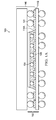
- Figure 1A illustrates a cross sectional view of the package-on-package semiconductor device 100.
- Figure 1A illustrates a top semiconductor package unit 140 (e . g ., flip chip memory device) stacked on top of a bottom semiconductor package unit 150 ( e . g ., memory controller).
- the top semiconductor package unit 140 is electrically coupled to the bottom semiconductor unit 150 by way of bumps 101 and top-side connector pads 114A-114B.
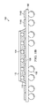
- Figure 1B illustrates the cross sectional view of the bottom semiconductor package unit 150 as a flip chip assembly coupled to a substrate 102 ( e .
- the bottom semiconductor package unit 150 electrically couples to the substrate 102 by way of the bumps 104 (e . g ., solder bumps, gold stud bumps).
- the bumps 104 provide an electrically conducting path between an integrated circuit die 112 and conducting pads 106 on the substrate 102.
- a non-conductive underfill adhesive 110 fills the portion between the integrated circuit die 112 and the substrate 102, the underfill adhesive 110 attaches , at least in part, the flip chip integrated circuit die 112 to the substrate 102.
- External bumps 108 connect the bottom semiconductor package unit 150 to a system level printed circuit board (not shown in Figure 1 ).
- the top semiconductor package unit 140 is electrically coupled to the bottom semiconductor package unit 150 by way of top-side connector pads 114A-114B.
- the top-side connector pad 114A provides an output from the bottom semiconductor package unit 150 to top semiconductor package unit
- the top-side connector pad 114B provides an input into the bottom semiconductor package unit 150 from the top semiconductor package unit.
- the top-side connector pad 114A provides the input while the top-side connector pad 114B provides the output.
- FIG. 2 illustrates a cross sectional view of a testing system 200 for testing the bottom semiconductor package unit 150.
- the testing system 200 as illustrated in Figure 2 , comprises a top printed circuit board 208 positioned above and parallel to the bottom semiconductor package unit 150, and a bottom printed circuit board 210 positioned below and parallel to the bottom semiconductor package unit 150.
- a plurality of top-side pogo pins 201A electrically couple the top printed circuit board 208 to the top-side connector pads 114A-114B of the bottom semiconductor package unit 150.
- Each of the top-side pogo pins 201A comprises an elongated barrel 202A and a probe pin 204A.
- the barrels 202A are spring loaded enabling the probe pins 204A to longitudinally compress against the top-side connector pads 114A-114B. Collectively, the barrels 202A and the probe pins 204A form an electrically conductive path from the top printed circuit board 208 to the top-side connector pads 114A-114B of the bottom semiconductor package unit 150.
- a plurality of bottom-side pogo pins 201B electrically couple the bottom printed circuit board 210 to the bottom-side connector pads 220 below the bottom semiconductor package unit 150.
- Each of the bottom-side pogo pins 201B comprises an elongated barrel 202B and a probe pin 204B.
- the barrels 202B are spring loaded enabling the probe pins 204B to longitudinally compress against the bottom-side connector pads 220. Collectively, the barrels 202B and the probe pins 204B form an electrically conductive path from the bottom printed circuit board 210 to the bottom-side connector pads 220 below the bottom semiconductor package unit 150. In alternative embodiments, a plurality of bottom-side pogo pins 201B electrically couple the bottom printed circuit board 210 to the external bumps 108 below the bottom semiconductor package unit 150. In at least some embodiments, the top-side pogo pins 201A and the bottom-side pogo pins 201B are of substantially equal height "h".
- a pair of adjacent top-side pogo pins 204A are electrically bridged together on the top printed circuit board 208.
- Figure 3 illustrates a top view of a portion of the top printed circuit board 208.
- the pogo pins 201A are electrically coupled using electrically conductive path 302.
- the electrically conductive path 302 is etched in the top printed circuit board 208. Consequently, the electrically conductive path 302 bridges a top-side pogo pin 201A with the adjacent top-side pogo pin 201A.
- one of the bridged top-side pogo pins 201A receives a signal outputted from the bottom semiconductor package 150, the signal is routed through the electrically conductive path 302 and the signal is inputted to the bottom semiconductor package 150 by way of the adjacent top-side pogo pin 201A.
- the testing system 200 as illustrated in the Figure 2 and Figure 3 performs continuity tests and functional tests of the bottom semiconductor package unit 150.
- the bottom printed circuit board 210 transmits electrical test signals to the bottom semiconductor package unit 150 by way of the electrically conductive path created by the bottom-side pogo pins 201B.
- the test signal is generated by a signal generator, not shown in Figure 2 , coupled to the bottom printed circuit board 210.
- the test signal is outputted by the bottom semiconductor package unit 150, and routed through the top-side connector pad 114A, and pogo pin 201A. Additionally, the test signal is routed through the electrically conductive path 302, pogo pin 201A, and inputted into the bottom semiconductor package unit 150 through the top-side connector pad 114B.
- the testing system 200 performs the continuity tests by transmitting a test signal (e . g . a sequence of bits) from the bottom printed circuit board 210 to the bottom semiconductor package unit 150.
- a test signal e . g . a sequence of bits
- the bottom semiconductor package unit 150 is a memory controller to be stacked below a memory device ( e . g ., flash memory, SDRAM, DDR) in the package-on-package semiconductor device.
- the continuity test for the memory controller comprises writing test data to an address in the memory device.
- the bottom printed circuit board 210 transmits a test signal with write test data that causes the bottom semiconductor package unit 150 (i.e ., the memory controller) to write test data to an address in the top semiconductor package unit 140 ( i.e ., the memory device).
- the test signal is routed through the bottom semiconductor package unit 150, and the bottom semiconductor package unit 150 outputs the write test data from the top-side connector 114A.
- the write test data is routed through the top-side pogo pin 201A, through the electrical path 302, through the top-side pogo pin 201A, and supplied again into the bottom semiconductor package unit 150 by the top-side connector pad 114B.
- the write test data is received by the bottom printed circuit board 210 through the bottom-side pogo pins 201B, and the bottom printed circuit board 210 compares the received write test data with the transmitted write test data. If the received write test data is different from the transmitted test data then the bottom semiconductor package unit 150 is determined to have failed the continuity test. Similarly, if the received write test data is same as the transmitted write test data then the semiconductor package unit 100 is determined to have passed the continuity test.
- the testing systems are not enabled to perform functional tests of the semiconductor package unit because the testing systems comprise pogo pins of various lengths. For example, there may be pogo pins that electrically couple the top printed circuit board directly to the bottom printed circuit board.
- the top printed circuit board as illustrated in Figure 3 enables the testing system as illustrated in Figure 2 to comprise pogo pins of substantially the same length "h".
- the testing system as illustrated in Figure 2 and 3 may perform functional tests of the bottom semiconductor package unit 150.
- the functional tests may be specific to the bottom semiconductor package unit 150.
- the bottom semiconductor package unit 150 is a memory controller to be stacked below a memory device ( e .
- the functional test for the memory controller comprises measuring the time to access the memory device.
- the testing system 200 measures access time of the memory controller by capturing at the top-side connector pad 114B a signal outputted from the top-side connector pad 114A.
- the bottom printed circuit board 210 transmits a test signal with write test data that causes the bottom semiconductor package unit 150 ( i.e ., the memory controller) to write test data to an address in the top semiconductor package unit 140 ( i.e ., the memory device).
- a propagation delay is measured as the write test data outputted by the top-side connector pad 114A is routed through the top-side pogo pin 201A, through the electrically conductive path 302, and captured at the top-side connector 114B.
- the propagation delay from the top-side connector 114A to the top-side connector 114B is a measure of the access time of the bottom semiconductor package unit 150.
- Figure 4 shows a method in accordance with at least some embodiments.
- method starts (block 410) and proceeds to testing a semiconductor package unit by electrically coupling a top printed circuit board to a top-side of a semiconductor package unit, the coupling using electrically conductive top-side pogo pins, and a pair of adjacent top-side pogo pins bridged using an electrically conductive path (block 420).
- the top-side pogo pins are bridged by etching an electrically conductive path in the top printed circuit board.
- a bottom printed circuit board is coupled to a bottom-side of the semiconductor package unit, the bottom printed circuit board is coupled using electrically conductive bottom-side pogo pins (block 430).
- the top-side pogo pins and the bottom-side pogo pins are of substantially equal height.
- the bottom printed circuit board transmits test signals to the semiconductor device package by way of the bottom-side pogo pins (block 440). The method then ends (block 450).
- testing of the semiconductor package unit may be performed using any other semiconductor package unit (e.g . ball grid array (BGA), pin grid array (PGA), etc.).
- BGA ball grid array
- PGA pin grid array
- the various embodiments are discussed with the functional test performed for the memory controller; however, the functional test may be performed for other semiconductor device (e.g . a micro controller, a digital signal processor, etc.).
- the various embodiments may perform testing of additional top-side connector pads (not specifically illustrated) by utilizing the bottom printed circuit board. It is intended that the following claims be interpreted to embrace all such variations and modifications.
Landscapes
- Engineering & Computer Science (AREA)
- General Engineering & Computer Science (AREA)
- Physics & Mathematics (AREA)
- General Physics & Mathematics (AREA)
- Computer Hardware Design (AREA)
- Microelectronics & Electronic Packaging (AREA)
- Tests Of Electronic Circuits (AREA)
Abstract
Description
- Electronic devices are continually getting smaller, faster, and using less power, while simultaneously being able to support and perform a greater number of increasingly complex and sophisticated functions. One reason for these trends is an ever increasing demand for small, portable and multifunctional electronic devices. For example, cellular phones, personal computing devices, and personal audio devices (e.g., MP3 players) are in great demand in the consumer market. Such electronic devices rely on a limited power source (e.g., batteries) while providing ever-increasing processing capabilities and storage capacity.
- Accordingly, there is a trend in the semiconductor industry to manufacture package-on-package semiconductor devices. A package-on-package semiconductor device involves stacking two or more semiconductor packages on top of each other. For example, a package-on-package semiconductor device may involve stacking a memory device (e.g. flash memory, SDRAM, etc.) on top of a memory controller. Package-on-package semiconductor devices keep the cost of manufacturing lower and provide higher yield.
- At least some of the illustrative embodiments are methods comprising testing a semiconductor package unit by electrically coupling a top printed circuit board to a top-side of a semiconductor package unit, the coupling using electrically conductive top-side pogo pins, a pair of adjacent top-side pogo pins bridged using an electrically conductive path, electrically coupling a bottom printed circuit board to a bottom-side of the semiconductor package unit, the coupling using electrically conductive bottom-side pogo pins, said top-side pogo pins and said bottom-side pogo pins are of substantially equal height, and transmitting test signals from the bottom printed circuit board to the semiconductor device package by way of the bottom-side pogo pins.
- Other illustrative embodiments are systems for testing a semiconductor package unit comprising a top printed circuit board comprising a plurality of barrels, each of the plurality of barrels comprises an electrically conductive pogo pin having a particular length, and each pogo pin configured to electrically couple to a top-side connector on a semiconductor package unit, and electrically conductive paths configured to bridge a pair adjacent barrels, a bottom printed circuit board comprising plurality of barrels, each of the plurality of barrels comprises an electrically conductive pogo pin having substantially the particular length, each pogo pin configured to electrically couple to a bottom-side connector on the semiconductor package unit, and said bottom printed circuit board configured to transmit test signals to the semiconductor package unit by way of the barrels.
- Yet other illustrative embodiments are an apparatus comprising a printed circuit board configured to be disposed on a top-side of semiconductor package unit, the printed circuit board comprising a plurality of barrels, each of the plurality of barrels comprises an electrically conductive pogo pin, and each pogo pin configured to electrically couple to a top-side connector on a semiconductor package unit; said each pogo pin is of substantially equal height, and electrically conductive paths configured to couple a pair adjacent barrels; and said printed circuit board is configured to enable a test of the semiconductor package unit.
- For a more detailed description of the various embodiments, reference will now be made to the accompanying drawings, wherein:
-
Figure 1A shows a package-on-package semiconductor device; -
Figure 1B shows a bottom semiconductor package unit of the package-on-package semiconductor device; -
Figure 2 shows a testing system in accordance with some embodiments; -
Figure 3 shows a top view of the top printed circuit board; and -
Figure 4 shows a method in accordance with at least some embodiments. - Certain terms are used throughout the following description and claims to refer to particular system components. As one skilled in the art will appreciate, various companies may refer to a component by different names. This document does not intend to distinguish between components that differ in name but not function. In the following discussion and in the claims, the terms "including" and "comprising" are used in an open-ended fashion, and thus should be interpreted to mean "including, but not limited to...". Also, the term "couple" or "couples" is intended to mean either an indirect or direct connection. Thus, if a first device couples to a second device, that connection may be through a direct connection, or through an indirect connection via other devices and connections.
- Unless otherwise stated, the term "semiconductor package unit" means a device having contact points on the top-side and the bottom-side of the device.
- The following discussion is directed to various embodiments.
Although one or more of these embodiments may be preferred, the embodiments disclosed should not be interpreted, or otherwise used, as limiting the scope of the disclosure, including the claims, unless otherwise specified. In addition, one skilled in the art will understand that the following description has broad application, and the discussion of any embodiment is meant only to be exemplary of that embodiment, and not intended to intimate that the scope of the disclosure, including the claims, is limited to that embodiment. - The various embodiments are directed to methods and related systems for testing a bottom semiconductor package unit of a package-on-package semiconductor device.
Figure 1A illustrates a cross sectional view of the package-on-package semiconductor device 100. In particular,Figure 1A illustrates a top semiconductor package unit 140 (e.g., flip chip memory device) stacked on top of a bottom semiconductor package unit 150 (e.g., memory controller). The topsemiconductor package unit 140 is electrically coupled to thebottom semiconductor unit 150 by way ofbumps 101 and top-side connector pads 114A-114B.Figure 1B illustrates the cross sectional view of the bottomsemiconductor package unit 150 as a flip chip assembly coupled to a substrate 102 (e.g., a printed circuit board, or a semiconductor tape). The bottomsemiconductor package unit 150 electrically couples to thesubstrate 102 by way of the bumps 104 (e.g., solder bumps, gold stud bumps). Thebumps 104 provide an electrically conducting path between an integratedcircuit die 112 and conductingpads 106 on thesubstrate 102. Anon-conductive underfill adhesive 110 fills the portion between theintegrated circuit die 112 and thesubstrate 102, the underfill adhesive 110 attaches , at least in part, the flip chip integrated circuit die 112 to thesubstrate 102.External bumps 108 connect the bottomsemiconductor package unit 150 to a system level printed circuit board (not shown inFigure 1 ). As previously discussed, the topsemiconductor package unit 140 is electrically coupled to the bottomsemiconductor package unit 150 by way of top-side connector pads 114A-114B. In at least some embodiments, the top-side connector pad 114A provides an output from the bottomsemiconductor package unit 150 to top semiconductor package unit, and the top-side connector pad 114B provides an input into the bottomsemiconductor package unit 150 from the top semiconductor package unit. In other embodiments, the top-side connector pad 114A provides the input while the top-side connector pad 114B provides the output. -
Figure 2 illustrates a cross sectional view of atesting system 200 for testing the bottomsemiconductor package unit 150. Thetesting system 200, as illustrated inFigure 2 , comprises a top printedcircuit board 208 positioned above and parallel to the bottomsemiconductor package unit 150, and a bottom printedcircuit board 210 positioned below and parallel to the bottomsemiconductor package unit 150. A plurality of top-side pogo pins 201A electrically couple the top printedcircuit board 208 to the top-side connector pads 114A-114B of the bottomsemiconductor package unit 150. Each of the top-side pogo pins 201A comprises anelongated barrel 202A and aprobe pin 204A. Thebarrels 202A are spring loaded enabling theprobe pins 204A to longitudinally compress against the top-side connector pads 114A-114B. Collectively, thebarrels 202A and theprobe pins 204A form an electrically conductive path from the top printedcircuit board 208 to the top-side connector pads 114A-114B of the bottomsemiconductor package unit 150. A plurality of bottom-side pogo pins 201B electrically couple the bottom printedcircuit board 210 to the bottom-side connector pads 220 below the bottomsemiconductor package unit 150. Each of the bottom-side pogo pins 201B comprises anelongated barrel 202B and aprobe pin 204B. Thebarrels 202B are spring loaded enabling theprobe pins 204B to longitudinally compress against the bottom-side connector pads 220. Collectively, thebarrels 202B and theprobe pins 204B form an electrically conductive path from the bottom printedcircuit board 210 to the bottom-side connector pads 220 below the bottomsemiconductor package unit 150. In alternative embodiments, a plurality of bottom-side pogo pins 201B electrically couple the bottom printedcircuit board 210 to theexternal bumps 108 below the bottomsemiconductor package unit 150. In at least some embodiments, the top-side pogo pins 201A and the bottom-side pogo pins 201B are of substantially equal height "h". - In at least some embodiments, a pair of adjacent top-
side pogo pins 204A are electrically bridged together on the top printedcircuit board 208.Figure 3 illustrates a top view of a portion of the top printedcircuit board 208. In accordance withFigure 3 , thepogo pins 201A are electrically coupled using electricallyconductive path 302. In at least some embodiments, the electricallyconductive path 302 is etched in the top printedcircuit board 208. Consequently, the electricallyconductive path 302 bridges a top-side pogo pin 201A with the adjacent top-side pogo pin 201A. As will be thoroughly discussed below, one of the bridged top-side pogo pins 201A receives a signal outputted from thebottom semiconductor package 150, the signal is routed through the electricallyconductive path 302 and the signal is inputted to thebottom semiconductor package 150 by way of the adjacent top-side pogo pin 201A. - The
testing system 200 as illustrated in theFigure 2 andFigure 3 performs continuity tests and functional tests of the bottomsemiconductor package unit 150. The bottom printedcircuit board 210 transmits electrical test signals to the bottomsemiconductor package unit 150 by way of the electrically conductive path created by the bottom-side pogo pins 201B. In at least some embodiments, the test signal is generated by a signal generator, not shown inFigure 2 , coupled to the bottom printedcircuit board 210. The test signal is outputted by the bottomsemiconductor package unit 150, and routed through the top-side connector pad 114A, andpogo pin 201A. Additionally, the test signal is routed through the electricallyconductive path 302,pogo pin 201A, and inputted into the bottomsemiconductor package unit 150 through the top-side connector pad 114B. - In at least some embodiments, the
testing system 200 performs the continuity tests by transmitting a test signal (e.g. a sequence of bits) from the bottom printedcircuit board 210 to the bottomsemiconductor package unit 150. Consider, for purpose of explanation, that the bottomsemiconductor package unit 150 is a memory controller to be stacked below a memory device (e.g., flash memory, SDRAM, DDR) in the package-on-package semiconductor device. The continuity test for the memory controller comprises writing test data to an address in the memory device. The bottom printedcircuit board 210 transmits a test signal with write test data that causes the bottom semiconductor package unit 150 (i.e., the memory controller) to write test data to an address in the top semiconductor package unit 140 (i.e., the memory device). The test signal is routed through the bottomsemiconductor package unit 150, and the bottomsemiconductor package unit 150 outputs the write test data from the top-side connector 114A. The write test data is routed through the top-side pogo pin 201A, through theelectrical path 302, through the top-side pogo pin 201A, and supplied again into the bottomsemiconductor package unit 150 by the top-side connector pad 114B. The write test data is received by the bottom printedcircuit board 210 through the bottom-side pogo pins 201B, and the bottom printedcircuit board 210 compares the received write test data with the transmitted write test data. If the received write test data is different from the transmitted test data then the bottomsemiconductor package unit 150 is determined to have failed the continuity test. Similarly, if the received write test data is same as the transmitted write test data then thesemiconductor package unit 100 is determined to have passed the continuity test. - In at least some related art, the testing systems are not enabled to perform functional tests of the semiconductor package unit because the testing systems comprise pogo pins of various lengths. For example, there may be pogo pins that electrically couple the top printed circuit board directly to the bottom printed circuit board. The top printed circuit board as illustrated in
Figure 3 enables the testing system as illustrated inFigure 2 to comprise pogo pins of substantially the same length "h". Thus, the testing system as illustrated inFigure 2 and3 may perform functional tests of the bottomsemiconductor package unit 150. In at least some embodiments, the functional tests may be specific to the bottomsemiconductor package unit 150. Consider, for purpose of explanation, that the bottomsemiconductor package unit 150 is a memory controller to be stacked below a memory device (e.g., flash memory, SDRAM, DDR) in the package-on-package semiconductor device. The functional test for the memory controller comprises measuring the time to access the memory device. Thetesting system 200 measures access time of the memory controller by capturing at the top-side connector pad 114B a signal outputted from the top-side connector pad 114A. For example, the bottom printedcircuit board 210 transmits a test signal with write test data that causes the bottom semiconductor package unit 150 (i.e., the memory controller) to write test data to an address in the top semiconductor package unit 140 (i.e., the memory device). A propagation delay is measured as the write test data outputted by the top-side connector pad 114A is routed through the top-side pogo pin 201A, through the electricallyconductive path 302, and captured at the top-side connector 114B. The propagation delay from the top-side connector 114A to the top-side connector 114B is a measure of the access time of the bottomsemiconductor package unit 150. -
Figure 4 shows a method in accordance with at least some embodiments. In particular, method starts (block 410) and proceeds to testing a semiconductor package unit by electrically coupling a top printed circuit board to a top-side of a semiconductor package unit, the coupling using electrically conductive top-side pogo pins, and a pair of adjacent top-side pogo pins bridged using an electrically conductive path (block 420). In some embodiments, the top-side pogo pins are bridged by etching an electrically conductive path in the top printed circuit board. Next, a bottom printed circuit board is coupled to a bottom-side of the semiconductor package unit, the bottom printed circuit board is coupled using electrically conductive bottom-side pogo pins (block 430). In at least some embodiments, the top-side pogo pins and the bottom-side pogo pins are of substantially equal height. The bottom printed circuit board transmits test signals to the semiconductor device package by way of the bottom-side pogo pins (block 440). The method then ends (block 450). - The above discussion is meant to be illustrative of the principles and various embodiments of the present invention. Numerous variations and modifications will become apparent to those skilled in the art once the above disclosure is fully appreciated. For example, the testing of the semiconductor package unit may be performed using any other semiconductor package unit (e.g. ball grid array (BGA), pin grid array (PGA), etc.). Moreover, the various embodiments are discussed with the functional test performed for the memory controller; however, the functional test may be performed for other semiconductor device (e.g. a micro controller, a digital signal processor, etc.). Finally, the various embodiments may perform testing of additional top-side connector pads (not specifically illustrated) by utilizing the bottom printed circuit board. It is intended that the following claims be interpreted to embrace all such variations and modifications.
Claims (16)
- A method comprising:testing a semiconductor package unit (150, 420) by:electrically coupling a top printed circuit board (208, 420) to a top-side of a semiconductor package unit (150, 420), the coupling using electrically conductive top-side pogo pins (201A, 420), and a pair of adjacent top-side pogo pins (201A, 420) bridged using an electrically conductive path (302, 420);electrically coupling a bottom printed circuit board (210, 430) to a bottom-side of the semiconductor package unit (150, 430), the coupling using electrically conductive bottom-side pogo pins (201B, 430), said top-side pogo pins (201A, 430) and said bottom-side pogo pins are of substantially equal height (201B, 430); andtransmitting test signals from the bottom printed circuit board to the semiconductor device package by way of the bottom-side pogo pins (210, 440).
- The method as defined in claim 1 further comprises performing a functional test (150, 440).
- The method as defined in claim 2 wherein performing the functional test further comprises measuring memory access time of the semiconductor package unit being a memory controller (150, 440).
- The method as defined in claim 3 wherein measuring memory access time further comprises measuring a propagation delay from a connector providing an output (114A, 440) from the semiconductor package unit to a connector providing an input (114B, 440) to the semiconductor package unit.
- The method as defined in any preceding claim wherein bridging further comprises bridging a pogo pin (201A, 440) electrically coupled to a connector providing an input (114A, 440) to the semiconductor package unit with a pogo pin (201A, 440) electrically coupled to a connector providing an output (114B, 440) from the semiconductor package unit.
- An apparatus comprising:a printed circuit board (208) configured to be disposed on a top-side of semiconductor package unit (150), the printed circuit board comprising:a plurality of electrically conductive pogo pins (201A), and each pogo pin configured to electrically couple to a top-side connector (114A) on a semiconductor package unit (150); said each pogo pin is of substantially equal height (201A); andelectrically conductive paths (302) configured to bridge a pair adjacent pogo pins (201A); andsaid printed circuit board (208) is configured to enable a test of the semiconductor package unit (150).
- The apparatus as defined in claim 6 wherein the pair of adjacent barrels (204A) further comprise a pogo pin (202A) electrically coupled to a connector configured to provide an input (114A) to the semiconductor package (150) and a pogo pin (202A) electrically coupled to a connector configured to provide an output (114B) from the semiconductor package unit.
- The apparatus as defined in claim 6 or claim 7 wherein the printed circuit board (208) is configured to enable a functional test of the semiconductor package unit (150).
- The apparatus as defined in claim 8 wherein the printed circuit board (208) configured to enable the functional test is further configured to enable a measure of memory access time of the semiconductor package unit being a memory controller.
- The apparatus as defined in claim 9 wherein the printed circuit board (208) configured to enable the measure of memory access time is further configured to enable a measure of propagation delay from a connector configured to provide an output (114B) from the semiconductor package unit to a connector configured to provide an input (114A) to the semiconductor package unit.
- A system to test a semiconductor package unit comprising:a top printed circuit board comprising:a plurality of electrically conductive pogo pins having a particular length, and each pogo pin configured to electrically couple to a top-side connector on a semiconductor package unit; andelectrically conductive paths configured to bridge a pair adjacent pogo pins;a bottom printed circuit board comprising:plurality of electrically conductive pogo pins having substantially the particular length, each pogo pin configured to electrically couple to a bottom-side connector on the semiconductor package unit; andsaid bottom printed circuit board configured to transmit test signals to the semiconductor package unit by way of the pogo pins.
- The system as defined in claim 11 wherein the system to test the semiconductor package unit is further configured to perform a continuity test of the semiconductor package unit.
- The system as defined in claim 11 wherein the system to test the semiconductor package unit is further configured to perform a functional test of the semiconductor package unit.
- The system as defined in claim 13 wherein the system configured to perform the functional test is further configured to measure memory access time of the semiconductor package unit being a memory controller.
- The system as defined in claim 14 wherein the system configured to measure memory access time further configured to measure propagation delay from a connector configured to provide an output from the semiconductor package unit to a connector configured to provide an input to the semiconductor package unit.
- The system as defined in any of claims 11 to 15 wherein the pair of adjacent pogo pins further comprise a pogo pin electrically coupled to a connector configured to provide an input to the semiconductor package unit and a pogo pin electrically coupled to a connector configured to provide an output from the semiconductor package unit.
Priority Applications (2)
| Application Number | Priority Date | Filing Date | Title |
|---|---|---|---|
| EP08157780A EP2131204B1 (en) | 2008-06-06 | 2008-06-06 | A method and system for testing a semiconductor package |
| US12/276,496 US8159244B2 (en) | 2008-06-06 | 2008-11-24 | Method and system for testing a semiconductor package |
Applications Claiming Priority (1)
| Application Number | Priority Date | Filing Date | Title |
|---|---|---|---|
| EP08157780A EP2131204B1 (en) | 2008-06-06 | 2008-06-06 | A method and system for testing a semiconductor package |
Publications (2)
| Publication Number | Publication Date |
|---|---|
| EP2131204A1 true EP2131204A1 (en) | 2009-12-09 |
| EP2131204B1 EP2131204B1 (en) | 2012-11-14 |
Family
ID=39877813
Family Applications (1)
| Application Number | Title | Priority Date | Filing Date |
|---|---|---|---|
| EP08157780A Ceased EP2131204B1 (en) | 2008-06-06 | 2008-06-06 | A method and system for testing a semiconductor package |
Country Status (2)
| Country | Link |
|---|---|
| US (1) | US8159244B2 (en) |
| EP (1) | EP2131204B1 (en) |
Cited By (1)
| Publication number | Priority date | Publication date | Assignee | Title |
|---|---|---|---|---|
| CN104237755A (en) * | 2014-09-30 | 2014-12-24 | 如皋市大昌电子有限公司 | Insulating and voltage-resistant testing tool for bridge rectifier |
Families Citing this family (4)
| Publication number | Priority date | Publication date | Assignee | Title |
|---|---|---|---|---|
| US9230682B2 (en) * | 2012-12-26 | 2016-01-05 | Broadcom Corporation | Method and system for automated device testing |
| KR102642193B1 (en) * | 2018-10-24 | 2024-03-05 | 삼성전자주식회사 | Device and method for testing semiconductor device and test handler |
| US12241912B2 (en) * | 2021-10-22 | 2025-03-04 | Raytheon Company | Socketless or flush mount QFN (quad flat no lead) test board, fixture, and method |
| FR3139411B1 (en) * | 2022-09-01 | 2025-10-24 | St Microelectronics Grenoble 2 | INTEGRATED CIRCUIT BOX |
Citations (5)
| Publication number | Priority date | Publication date | Assignee | Title |
|---|---|---|---|---|
| US4056773A (en) * | 1976-08-25 | 1977-11-01 | Sullivan Donald F | Printed circuit board open circuit tester |
| EP0492806A2 (en) * | 1990-12-20 | 1992-07-01 | Hewlett-Packard Company | Identification of pin-open faults by capacitive coupling through the integrated circuit package |
| US20070173097A1 (en) * | 2006-01-25 | 2007-07-26 | Samsung Electronics Co., Ltd. | Socket for an electrical tester |
| US20080054910A1 (en) * | 2006-09-05 | 2008-03-06 | Inventec Appliances Corp. | Test apparatus for testing operation of a printed circuit board |
| US20080094086A1 (en) * | 2006-10-24 | 2008-04-24 | Samsung Electronics Co., Ltd | Stack-type semiconductor package sockets and stack-type semiconductor package test systems |
Family Cites Families (18)
| Publication number | Priority date | Publication date | Assignee | Title |
|---|---|---|---|---|
| US5150041A (en) * | 1991-06-21 | 1992-09-22 | Compaq Computer Corporation | Optically alignable printed circuit board test fixture apparatus and associated methods |
| US5818248A (en) * | 1996-07-29 | 1998-10-06 | Delaware Capital Formation, Inc | Loaded board test fixture with integral translator fixture for testing closely spaced test sites |
| DE19654404A1 (en) * | 1996-12-24 | 1998-06-25 | Hewlett Packard Co | Adaptation device for the electrical test of printed circuit boards |
| US6551844B1 (en) * | 1997-01-15 | 2003-04-22 | Formfactor, Inc. | Test assembly including a test die for testing a semiconductor product die |
| JP3214415B2 (en) * | 1997-10-30 | 2001-10-02 | 日本電産リード株式会社 | Substrate inspection device and substrate inspection method |
| JP2000338167A (en) * | 1999-05-31 | 2000-12-08 | Nidec-Read Corp | Circuit board inspection device |
| US6700398B1 (en) * | 2000-11-28 | 2004-03-02 | Kingston Technology Company | In-line D.C. testing of multiple memory modules in a panel before panel separation |
| US6791344B2 (en) * | 2000-12-28 | 2004-09-14 | International Business Machines Corporation | System for and method of testing a microelectronic device using a dual probe technique |
| US6798225B2 (en) * | 2002-05-08 | 2004-09-28 | Formfactor, Inc. | Tester channel to multiple IC terminals |
| US6903360B2 (en) * | 2002-10-16 | 2005-06-07 | Agilent Technologies, Inc. | Method for detecting missing components at electrical board test using optoelectronic fixture-mounted sensors |
| US7102372B2 (en) * | 2004-11-02 | 2006-09-05 | Taiwan Semiconductor Manufacturing Co., Ltd. | Apparatus and method for testing conductive bumps |
| US7187165B2 (en) * | 2004-12-10 | 2007-03-06 | Agilent Technologies, Inc. | Method and system for implicitly encoding preferred probing locations in a printed circuit board design for use in tester fixture build |
| US7196294B2 (en) * | 2005-02-28 | 2007-03-27 | Ridgetop Group, Inc. | Method and resistive bridge circuit for the detection of solder-joint failures in a digital electronic package |
| US20060250149A1 (en) * | 2005-05-04 | 2006-11-09 | Unitech Printed Circuit Board Corp. | Complex printed circuit board testing tool |
| US7271606B1 (en) * | 2005-08-04 | 2007-09-18 | National Semiconductor Corporation | Spring-based probe pin that allows kelvin testing |
| JP4767147B2 (en) * | 2005-11-16 | 2011-09-07 | パナソニック株式会社 | Inspection apparatus and inspection method |
| JP4571076B2 (en) * | 2006-01-23 | 2010-10-27 | 富士通セミコンダクター株式会社 | Inspection equipment for semiconductor devices |
| US7400135B1 (en) * | 2007-02-23 | 2008-07-15 | Quality One Test Fixturing, Inc. | Test fixture and method for circuit board testing |
-
2008
- 2008-06-06 EP EP08157780A patent/EP2131204B1/en not_active Ceased
- 2008-11-24 US US12/276,496 patent/US8159244B2/en active Active
Patent Citations (5)
| Publication number | Priority date | Publication date | Assignee | Title |
|---|---|---|---|---|
| US4056773A (en) * | 1976-08-25 | 1977-11-01 | Sullivan Donald F | Printed circuit board open circuit tester |
| EP0492806A2 (en) * | 1990-12-20 | 1992-07-01 | Hewlett-Packard Company | Identification of pin-open faults by capacitive coupling through the integrated circuit package |
| US20070173097A1 (en) * | 2006-01-25 | 2007-07-26 | Samsung Electronics Co., Ltd. | Socket for an electrical tester |
| US20080054910A1 (en) * | 2006-09-05 | 2008-03-06 | Inventec Appliances Corp. | Test apparatus for testing operation of a printed circuit board |
| US20080094086A1 (en) * | 2006-10-24 | 2008-04-24 | Samsung Electronics Co., Ltd | Stack-type semiconductor package sockets and stack-type semiconductor package test systems |
Cited By (2)
| Publication number | Priority date | Publication date | Assignee | Title |
|---|---|---|---|---|
| CN104237755A (en) * | 2014-09-30 | 2014-12-24 | 如皋市大昌电子有限公司 | Insulating and voltage-resistant testing tool for bridge rectifier |
| CN104237755B (en) * | 2014-09-30 | 2017-05-10 | 如皋市大昌电子有限公司 | Insulating and voltage-resistant testing tool for bridge rectifier |
Also Published As
| Publication number | Publication date |
|---|---|
| EP2131204B1 (en) | 2012-11-14 |
| US20090121735A1 (en) | 2009-05-14 |
| US8159244B2 (en) | 2012-04-17 |
Similar Documents
| Publication | Publication Date | Title |
|---|---|---|
| KR101341566B1 (en) | A socket, a test equipment, and method for manufacturing a multi-chip semiconductor device package | |
| JP5914541B2 (en) | Probe card | |
| US9589905B2 (en) | EMI shielding in semiconductor packages | |
| US20140014958A1 (en) | Semiconductor chip module and semiconductor package having the same | |
| KR101977699B1 (en) | Multi chip semiconductor apparatus and method of testing the same | |
| US10204661B2 (en) | Semiconductor device | |
| US7436199B2 (en) | Stack-type semiconductor package sockets and stack-type semiconductor package test systems | |
| US20130099235A1 (en) | Semiconductor wafer and method for manufacturing stack package using the same | |
| KR101697603B1 (en) | Semiconductor Package | |
| EP2131204B1 (en) | A method and system for testing a semiconductor package | |
| CN100505437C (en) | Contactor and testing method using contactor | |
| US20140264904A1 (en) | Unified pcb design for ssd applications, various density configurations, and direct nand access | |
| US9396765B2 (en) | Stacked semiconductor package | |
| US20150380062A1 (en) | Memory module and video camera | |
| US20160293230A1 (en) | Semiconductor device, a method for manufacturing the same, and a system having the same | |
| CN217133316U (en) | Chip testing tool and chip testing device | |
| TWI281035B (en) | Test board for high-frequency system level test | |
| US7414422B2 (en) | System in-package test inspection apparatus and test inspection method | |
| US20180040589A1 (en) | Microelectronic packages and assemblies with repeaters | |
| US7898279B2 (en) | Circuit for multi-pads test | |
| KR100871378B1 (en) | FAX Package Tester | |
| US10101381B2 (en) | Space transformation methods | |
| KR101311177B1 (en) | Probe card on mounted active element chip | |
| CN118259142A (en) | Package routing performance test circuit and method | |
| KR20160041330A (en) | Semiconductor package |
Legal Events
| Date | Code | Title | Description |
|---|---|---|---|
| PUAI | Public reference made under article 153(3) epc to a published international application that has entered the european phase |
Free format text: ORIGINAL CODE: 0009012 |
|
| AK | Designated contracting states |
Kind code of ref document: A1 Designated state(s): AT BE BG CH CY CZ DE DK EE ES FI FR GB GR HR HU IE IS IT LI LT LU LV MC MT NL NO PL PT RO SE SI SK TR |
|
| AX | Request for extension of the european patent |
Extension state: AL BA MK RS |
|
| 17P | Request for examination filed |
Effective date: 20100609 |
|
| 17Q | First examination report despatched |
Effective date: 20100705 |
|
| AKX | Designation fees paid |
Designated state(s): DE FR GB NL |
|
| REG | Reference to a national code |
Ref country code: DE Ref legal event code: R079 Ref document number: 602008020062 Country of ref document: DE Free format text: PREVIOUS MAIN CLASS: G01R0031319000 Ipc: G01R0031280000 |
|
| RIC1 | Information provided on ipc code assigned before grant |
Ipc: G01R 31/319 20060101ALI20120612BHEP Ipc: G01R 31/28 20060101AFI20120612BHEP Ipc: G01R 1/04 20060101ALI20120612BHEP |
|
| GRAP | Despatch of communication of intention to grant a patent |
Free format text: ORIGINAL CODE: EPIDOSNIGR1 |
|
| GRAS | Grant fee paid |
Free format text: ORIGINAL CODE: EPIDOSNIGR3 |
|
| GRAA | (expected) grant |
Free format text: ORIGINAL CODE: 0009210 |
|
| AK | Designated contracting states |
Kind code of ref document: B1 Designated state(s): DE FR GB NL |
|
| REG | Reference to a national code |
Ref country code: GB Ref legal event code: FG4D |
|
| REG | Reference to a national code |
Ref country code: DE Ref legal event code: R096 Ref document number: 602008020062 Country of ref document: DE Effective date: 20130110 |
|
| REG | Reference to a national code |
Ref country code: NL Ref legal event code: VDEP Effective date: 20121114 |
|
| PG25 | Lapsed in a contracting state [announced via postgrant information from national office to epo] |
Ref country code: NL Free format text: LAPSE BECAUSE OF FAILURE TO SUBMIT A TRANSLATION OF THE DESCRIPTION OR TO PAY THE FEE WITHIN THE PRESCRIBED TIME-LIMIT Effective date: 20121114 |
|
| PLBE | No opposition filed within time limit |
Free format text: ORIGINAL CODE: 0009261 |
|
| STAA | Information on the status of an ep patent application or granted ep patent |
Free format text: STATUS: NO OPPOSITION FILED WITHIN TIME LIMIT |
|
| 26N | No opposition filed |
Effective date: 20130815 |
|
| REG | Reference to a national code |
Ref country code: DE Ref legal event code: R097 Ref document number: 602008020062 Country of ref document: DE Effective date: 20130815 |
|
| REG | Reference to a national code |
Ref country code: FR Ref legal event code: PLFP Year of fee payment: 9 |
|
| REG | Reference to a national code |
Ref country code: FR Ref legal event code: PLFP Year of fee payment: 10 |
|
| REG | Reference to a national code |
Ref country code: FR Ref legal event code: PLFP Year of fee payment: 11 |
|
| P01 | Opt-out of the competence of the unified patent court (upc) registered |
Effective date: 20230523 |
|
| PGFP | Annual fee paid to national office [announced via postgrant information from national office to epo] |
Ref country code: GB Payment date: 20240521 Year of fee payment: 17 |
|
| PGFP | Annual fee paid to national office [announced via postgrant information from national office to epo] |
Ref country code: DE Payment date: 20240521 Year of fee payment: 17 |
|
| PGFP | Annual fee paid to national office [announced via postgrant information from national office to epo] |
Ref country code: FR Payment date: 20240521 Year of fee payment: 17 |
|
| REG | Reference to a national code |
Ref country code: DE Ref legal event code: R119 Ref document number: 602008020062 Country of ref document: DE |
|
| GBPC | Gb: european patent ceased through non-payment of renewal fee |
Effective date: 20250606 |
|
| PG25 | Lapsed in a contracting state [announced via postgrant information from national office to epo] |
Ref country code: GB Free format text: LAPSE BECAUSE OF NON-PAYMENT OF DUE FEES Effective date: 20250606 |
|
| PG25 | Lapsed in a contracting state [announced via postgrant information from national office to epo] |
Ref country code: DE Free format text: LAPSE BECAUSE OF NON-PAYMENT OF DUE FEES Effective date: 20260101 |
|
| PG25 | Lapsed in a contracting state [announced via postgrant information from national office to epo] |
Ref country code: FR Free format text: LAPSE BECAUSE OF NON-PAYMENT OF DUE FEES Effective date: 20250630 |