EP2128847A1 - Organic light emitting display device - Google Patents
Organic light emitting display device Download PDFInfo
- Publication number
- EP2128847A1 EP2128847A1 EP09157077A EP09157077A EP2128847A1 EP 2128847 A1 EP2128847 A1 EP 2128847A1 EP 09157077 A EP09157077 A EP 09157077A EP 09157077 A EP09157077 A EP 09157077A EP 2128847 A1 EP2128847 A1 EP 2128847A1
- Authority
- EP
- European Patent Office
- Prior art keywords
- output
- detection sensor
- lines
- external condition
- display device
- Prior art date
- Legal status (The legal status is an assumption and is not a legal conclusion. Google has not performed a legal analysis and makes no representation as to the accuracy of the status listed.)
- Granted
Links
Images

Classifications
-
- G—PHYSICS
- G09—EDUCATION; CRYPTOGRAPHY; DISPLAY; ADVERTISING; SEALS
- G09G—ARRANGEMENTS OR CIRCUITS FOR CONTROL OF INDICATING DEVICES USING STATIC MEANS TO PRESENT VARIABLE INFORMATION
- G09G3/00—Control arrangements or circuits, of interest only in connection with visual indicators other than cathode-ray tubes
- G09G3/20—Control arrangements or circuits, of interest only in connection with visual indicators other than cathode-ray tubes for presentation of an assembly of a number of characters, e.g. a page, by composing the assembly by combination of individual elements arranged in a matrix no fixed position being assigned to or needed to be assigned to the individual characters or partial characters
- G09G3/22—Control arrangements or circuits, of interest only in connection with visual indicators other than cathode-ray tubes for presentation of an assembly of a number of characters, e.g. a page, by composing the assembly by combination of individual elements arranged in a matrix no fixed position being assigned to or needed to be assigned to the individual characters or partial characters using controlled light sources
- G09G3/30—Control arrangements or circuits, of interest only in connection with visual indicators other than cathode-ray tubes for presentation of an assembly of a number of characters, e.g. a page, by composing the assembly by combination of individual elements arranged in a matrix no fixed position being assigned to or needed to be assigned to the individual characters or partial characters using controlled light sources using electroluminescent panels
- G09G3/32—Control arrangements or circuits, of interest only in connection with visual indicators other than cathode-ray tubes for presentation of an assembly of a number of characters, e.g. a page, by composing the assembly by combination of individual elements arranged in a matrix no fixed position being assigned to or needed to be assigned to the individual characters or partial characters using controlled light sources using electroluminescent panels semiconductive, e.g. using light-emitting diodes [LED]
- G09G3/3208—Control arrangements or circuits, of interest only in connection with visual indicators other than cathode-ray tubes for presentation of an assembly of a number of characters, e.g. a page, by composing the assembly by combination of individual elements arranged in a matrix no fixed position being assigned to or needed to be assigned to the individual characters or partial characters using controlled light sources using electroluminescent panels semiconductive, e.g. using light-emitting diodes [LED] organic, e.g. using organic light-emitting diodes [OLED]
- G09G3/3225—Control arrangements or circuits, of interest only in connection with visual indicators other than cathode-ray tubes for presentation of an assembly of a number of characters, e.g. a page, by composing the assembly by combination of individual elements arranged in a matrix no fixed position being assigned to or needed to be assigned to the individual characters or partial characters using controlled light sources using electroluminescent panels semiconductive, e.g. using light-emitting diodes [LED] organic, e.g. using organic light-emitting diodes [OLED] using an active matrix
-
- H—ELECTRICITY
- H10—SEMICONDUCTOR DEVICES; ELECTRIC SOLID-STATE DEVICES NOT OTHERWISE PROVIDED FOR
- H10P—GENERIC PROCESSES OR APPARATUS FOR THE MANUFACTURE OR TREATMENT OF DEVICES COVERED BY CLASS H10
- H10P14/00—Formation of materials, e.g. in the shape of layers or pillars
- H10P14/20—Formation of materials, e.g. in the shape of layers or pillars of semiconductor materials
- H10P14/38—Formation of materials, e.g. in the shape of layers or pillars of semiconductor materials characterised by treatments done after the formation of the materials
- H10P14/3802—Crystallisation or recrystallisation of non-monocrystalline semiconductor materials, e.g. regrowth
- H10P14/382—Scanning of a beam
-
- G—PHYSICS
- G09—EDUCATION; CRYPTOGRAPHY; DISPLAY; ADVERTISING; SEALS
- G09G—ARRANGEMENTS OR CIRCUITS FOR CONTROL OF INDICATING DEVICES USING STATIC MEANS TO PRESENT VARIABLE INFORMATION
- G09G2300/00—Aspects of the constitution of display devices
- G09G2300/04—Structural and physical details of display devices
- G09G2300/0421—Structural details of the set of electrodes
- G09G2300/0426—Layout of electrodes and connections
-
- G—PHYSICS
- G09—EDUCATION; CRYPTOGRAPHY; DISPLAY; ADVERTISING; SEALS
- G09G—ARRANGEMENTS OR CIRCUITS FOR CONTROL OF INDICATING DEVICES USING STATIC MEANS TO PRESENT VARIABLE INFORMATION
- G09G2320/00—Control of display operating conditions
- G09G2320/04—Maintaining the quality of display appearance
- G09G2320/041—Temperature compensation
-
- G—PHYSICS
- G09—EDUCATION; CRYPTOGRAPHY; DISPLAY; ADVERTISING; SEALS
- G09G—ARRANGEMENTS OR CIRCUITS FOR CONTROL OF INDICATING DEVICES USING STATIC MEANS TO PRESENT VARIABLE INFORMATION
- G09G2330/00—Aspects of power supply; Aspects of display protection and defect management
- G09G2330/06—Handling electromagnetic interferences [EMI], covering emitted as well as received electromagnetic radiation
-
- G—PHYSICS
- G09—EDUCATION; CRYPTOGRAPHY; DISPLAY; ADVERTISING; SEALS
- G09G—ARRANGEMENTS OR CIRCUITS FOR CONTROL OF INDICATING DEVICES USING STATIC MEANS TO PRESENT VARIABLE INFORMATION
- G09G2360/00—Aspects of the architecture of display systems
- G09G2360/14—Detecting light within display terminals, e.g. using a single or a plurality of photosensors
- G09G2360/144—Detecting light within display terminals, e.g. using a single or a plurality of photosensors the light being ambient light
-
- G—PHYSICS
- G09—EDUCATION; CRYPTOGRAPHY; DISPLAY; ADVERTISING; SEALS
- G09G—ARRANGEMENTS OR CIRCUITS FOR CONTROL OF INDICATING DEVICES USING STATIC MEANS TO PRESENT VARIABLE INFORMATION
- G09G3/00—Control arrangements or circuits, of interest only in connection with visual indicators other than cathode-ray tubes
- G09G3/20—Control arrangements or circuits, of interest only in connection with visual indicators other than cathode-ray tubes for presentation of an assembly of a number of characters, e.g. a page, by composing the assembly by combination of individual elements arranged in a matrix no fixed position being assigned to or needed to be assigned to the individual characters or partial characters
-
- G—PHYSICS
- G09—EDUCATION; CRYPTOGRAPHY; DISPLAY; ADVERTISING; SEALS
- G09G—ARRANGEMENTS OR CIRCUITS FOR CONTROL OF INDICATING DEVICES USING STATIC MEANS TO PRESENT VARIABLE INFORMATION
- G09G3/00—Control arrangements or circuits, of interest only in connection with visual indicators other than cathode-ray tubes
- G09G3/20—Control arrangements or circuits, of interest only in connection with visual indicators other than cathode-ray tubes for presentation of an assembly of a number of characters, e.g. a page, by composing the assembly by combination of individual elements arranged in a matrix no fixed position being assigned to or needed to be assigned to the individual characters or partial characters
- G09G3/22—Control arrangements or circuits, of interest only in connection with visual indicators other than cathode-ray tubes for presentation of an assembly of a number of characters, e.g. a page, by composing the assembly by combination of individual elements arranged in a matrix no fixed position being assigned to or needed to be assigned to the individual characters or partial characters using controlled light sources
- G09G3/30—Control arrangements or circuits, of interest only in connection with visual indicators other than cathode-ray tubes for presentation of an assembly of a number of characters, e.g. a page, by composing the assembly by combination of individual elements arranged in a matrix no fixed position being assigned to or needed to be assigned to the individual characters or partial characters using controlled light sources using electroluminescent panels
- G09G3/32—Control arrangements or circuits, of interest only in connection with visual indicators other than cathode-ray tubes for presentation of an assembly of a number of characters, e.g. a page, by composing the assembly by combination of individual elements arranged in a matrix no fixed position being assigned to or needed to be assigned to the individual characters or partial characters using controlled light sources using electroluminescent panels semiconductive, e.g. using light-emitting diodes [LED]
- G09G3/3208—Control arrangements or circuits, of interest only in connection with visual indicators other than cathode-ray tubes for presentation of an assembly of a number of characters, e.g. a page, by composing the assembly by combination of individual elements arranged in a matrix no fixed position being assigned to or needed to be assigned to the individual characters or partial characters using controlled light sources using electroluminescent panels semiconductive, e.g. using light-emitting diodes [LED] organic, e.g. using organic light-emitting diodes [OLED]
- G09G3/3266—Details of drivers for scan electrodes
Definitions
- the invention relates to an organic light emitting display device, and more particularly to an organic light emitting display device capable of stabilizing the output of a sensor for detecting an external condition.
- the flat panel displays are light-weight and small-sized, when compared to cathode ray tubes.
- the organic light emitting display device is favored with excellent luminance and color purity.
- the organic light emitting display uses an organic compound as a light emitting material.
- An organic light emitting display device is thin and light-weight and may be driven with low power consumption, and therefore it has been expected to be widely used in the field of portable display devices, etc.
- the organic light emitting display device may be exposed to various external environments. Therefore, the organic light emitting display device may have different visibilities according to the external conditions such as the intensity of ambient light, the ambient temperature, etc.
- an external condition detection sensor may be provided in the organic light emitting display device to output a detection signal by sensing the external conditions and control drive circuits according to the detection signal.
- the output of the external condition detection sensor may be a small current signal.
- a light detection sensor unit may output a light detection signal having a small current value.
- Such an output of the external condition detection sensor is easily affected by noise from peripheral circuits or signal lines. Therefore, it is difficult to accurately adjust the output luminance of the organic light emitting display device to a reliable luminance level that corresponds to the external conditions because the output of the external condition detection sensor is unstable.
- An aspect of the invention provides an organic light emitting display device as set forth in claim 1. Preferred embodiments of the invention are subject matter of the dependent claims.
- FIG. 1 is a plane view showing an organic light emitting display device according to one exemplary embodiment.
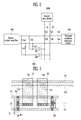
- FIG. 2 is a circuit diagram showing a configuration of a sensor output stabilizing unit as shown in FIG. 1 .
- FIG. 3 is a plane view showing a layout of the sensor output stabilizing unit as shown in FIG. 2 .
- first element When a first element is described as being coupled to a second element, the first element may not be directly coupled to the second element but may be indirectly coupled to the second element via a third element. Further, some of the elements that are not essential to the complete understanding of the invention are omitted for clarity. Also, like reference numerals generally refer to like elements throughout.
- FIG. 1 is a plane view showing an organic light emitting display device according to one exemplary embodiment.
- the organic light emitting display device includes a pixel unit 100, first and second scan drivers 200a and 200b, a data driver 300, an external condition detection sensor 400, a sensor output amplifier unit 500, a sensor output stabilizing unit 600, and a pad unit 700.
- the pixel unit 100 includes a plurality of pixels 110 disposed near intersection points of scan lines (S1 to Sn), light-emitting control lines (E1 to En) and data lines (D1 to Dm). Pixel unit 100 receives a scan signal, a light-emitting control signal and a data signal from the scan lines (S1 to Sn), the light-emitting control lines (E1 to En) and the data lines (D 1 to Dm), respectively. Also, the pixel unit 100 further receives first and second pixel power sources (ELVDD and ELVSS) through the pad unit 700. Pixel unit 100 displays an image according to the scan signal, the light-emitting control signal, the data signal, and the first and second pixel power sources (ELVDD and ELVSS).
- ELVDD and ELVSS first and second pixel power sources
- the first and second scan drivers 200a and 200b generate a scan signal and a light-emitting control signal according to the scan drive control signal supplied from the pad unit 700.
- the first scan driver 200a may receive a start pulse and a clock signal, an output enable signal and the like from the pad unit 700 to generate a scan signal, and generate a scan signal according to the received signals.
- the scan signal generated in the first scan driver 200a is subsequently supplied to the scan lines (S 1 to Sn).
- the second scan driver 200b may receive a start pulse, a clock signal and the like from the pad unit 700 to generate a light-emitting control signal, and generate a light-emitting control signal according to the received signals.
- the light-emitting control signal generated in the second scan driver 200b is subsequently supplied to the light-emitting control lines (E1 to En).
- the two scan drivers 200a and 200b are disposed on either side of the pixel unit 100 to supply a scan signal and a light-emitting control signal to the scan lines (S1 to Sn) and the light-emitting control lines (E1 to En) respectively, as shown in FIG. 1 , but the present invention is not limited thereto.
- one scan driver may generate both a scan signal and a light-emitting control signal, or may generate only a scan signal without generating a light-emitting control signal.
- the scan driver provided on one side of the pixel unit 100 may generate some of a scan signal and a light-emitting control signal, and the scan driver provided on the other side of the pixel unit 100 may generate the remainder of the scan signal and light-emitting control signals.
- the data driver 300 generates a data signal according to a data drive control signal and data supplied from the pad unit 700.
- the data signal generated in the data driver 300 is supplied to the data lines (D1 to Dm).
- the data driver 300 may be set to control the output luminance of the pixel unit 100 according to a detection signal output from the external condition detection sensor 400.
- the data driver 300 may control a voltage level of a data signal according to the detection signal in the case of a voltage drive method.
- the data driver 300 may control the current of the data signal according to the detection signal, for example, in the case of a current drive method.
- the external condition detection sensor 400 senses external condition, and outputs a detection signal corresponding to the external conditions.
- the external condition detection sensor 400 may have a light detection device to sense the intensity of ambient light, and output a light detection signal corresponding to the intensity of ambient light.
- the external condition detection sensor 400 may have a temperature detection device to sense an ambient temperature, and include a temperature detection sensor unit to output a temperature detection signal corresponding to the ambient temperature.
- the external condition detection sensor 400 has a light detection sensor unit and a temperature detection sensor unit.
- the external condition detection sensor 400 may be designed to output a light detection signal and a temperature detection signal separately.
- the sensor output amplifier unit 500 is coupled between the external condition detection sensor 400 and the data driver 300.
- the sensor output amplifier unit 500 includes an amplifier circuit for amplifying a current value (or, a voltage value) of the detection signals from the external condition detection sensor 400. That is to say, the sensor output amplifier unit 500 amplifies the detection signal supplied from the external condition detection sensor 400 and supplies the amplified detection signal to the data driver 300.
- the sensor output stabilizing unit 600 is coupled to an output line of the external condition detection sensor 400.
- the output stabilizing unit 600 is provided to stabilize the output of the external condition detection sensor 400, because the output line of the external condition detection sensor 400 is in a high-impedance state.
- the output of the external condition detection sensor 400 may be a small current value (for example, a current value of about 100nA or less).
- a separate power source is not connected to the output line of the external condition detection sensor 400, and the output line of the external condition detection sensor 400 is in a high-impedance state when the small electric current is output.
- the detection signal may be affected by peripheral circuits or other signal lines.
- the external condition detection sensor 400 and the sensor output amplifier unit 500 may be provided in a panel of the organic light emitting display device in consideration of the unit price.
- an output line of the external condition detection sensor 400 may be disposed so that the output line crosses at least some input lines and/or output lines (hereinafter, referred to as input/output lines) of the first and/or second scan drivers 200a and 200b.
- the input lines of the first and/or second scan drivers 200a and 200b includes lines for supplying a start pulse, a clock signal and/or driver power sources to drive the first and/or second scan drivers 200a and 200b.
- the output lines of the first and/or second scan drivers 200a and 200b may include lines for outputting a scan signal and/or a light-emitting control signal (for example, a scan signal and/or a light-emitting control signal of the last terminal), which are outputted from the first and/or second scan drivers 200a and 200b, through the pad unit 700, and test the scan signal and/or the light-emitting control signal.
- a scan signal and/or a light-emitting control signal for example, a scan signal and/or a light-emitting control signal of the last terminal
- the external condition detection sensor 400 and the sensor output amplifier unit 500 may be provided in upper and/or lower sides, away from the first and second drivers 200a and 200b.
- the external condition detection sensor 400 and the sensor output amplifier unit 500 may be disposed respectively in the upper and lower sides of the panel in consideration of the sizes of the external condition detection sensor 400 and the sensor output amplifier unit 500 and the spaces formed in the upper and lower sides of the panel.
- the sensor output amplifier unit 500 may be disposed on one side of the data driver 300 to reduce a distance to the data driver 300 and to facilitate the measurement of characteristics of an output terminal.
- the sensor output amplifier units 500 may be disposed in a lower side of the second scan driver 200b, as shown in FIG. 1 .
- the output lines of the external condition detection sensor 400 coupled from the external condition detection sensor 400 to the sensor output amplifier unit 500 may be formed so that the output lines of the external condition detection sensor 400 can cross the input/output lines of the second scan driver 200b. That is to say, parasitic capacitors may be formed between the output lines of the external condition detection sensor 400 and the output lines of the second scan driver 200b. Scan control signals for driving the second scan driver 200b is supplied to the input/output lines of the second scan driver 200b.
- the second scan driver 200b when the second scan driver 200b generates a light-emitting control signal, a light-emitting control start pulse, a first and second light-emitting control clock signal and an input power of the second scan driver 200b may be input through the input lines of the second scan driver 200b, respectively.
- a light-emitting control signal output to the last terminal of the second scan driver 200b may be output to the output lines of the second scan driver 200b to test the light-emitting control signal. That is to say, three input/output lines of the second scan driver 200b are shown in FIG. 1 for convenience' sake, but the number of the input/output lines may be widely varied according to the second scan driver 200b.
- some of the scan control signals and/or light-emitting control signals supplied to the input/output lines of the second scan driver 200b may affect the detection signal output to the output lines of the external condition detection sensor 400, and change the detection signal.
- alternating scan control signals and/or light-emitting control signals whose voltage levels repeatedly change may change the detection signal due to coupling through parasitic capacitors.
- the start pulse of the light-emitting control signal input to the input line of the second scan driver 200b, and the light-emitting control signal output to the output line of the second scan driver 200b may couple onto the detection signal line.
- a sensor output stabilizing unit 600 is connected to some of the input/output lines, of the input/output lines of the second scan driver 200b.
- the input/output lines are disposed so that they overlap the output line of the external condition detection sensor 400, and the output line of the external condition detection sensor 400.
- Some of the input/output lines are represented by L1 and L2, as shown in FIG. 1 .
- Some embodiments of the sensor output stabilizing unit 600 include at least an inverter and a capacitor to compensate for the changes in the voltage level caused by the coupling reaction, and further description thereof will given below.
- the pad unit 700 includes a plurality of pads (P) coupled to external drive circuits (not shown). Such a pad unit 700 transmits, for example, driver power sources and/or drive signals, supplied from each of the pads (P), to the panel.
- the pad unit 700 may supply the driver power sources and/or drive signals, supplied from each of the pads (P), into the pixel unit 100, the first and second scan drivers 200a and 200b, the data driver 300, the external condition detection sensor 400, the sensor output amplifier unit 500 and/or the sensor output stabilizing unit 600.
- the organic light emitting display device of FIG. 1 is configured to compensate for the changes in the detection signal caused by the coupling of the overlapped signal lines by coupling the sensor output stabilizing unit 600 to the output line of the external condition detection sensor 400.
- an organic light emitting display device that may reliably cope with the changes in the external conditions may be provided because the output of the external condition detection sensor 400 is stable.
- FIG. 1 shows that the sensor output amplifier unit 500 is disposed in a region below the second scan driver 200b, but the present invention is not limited thereto.
- the sensor output amplifier unit 500 may be disposed in a region below the first scan driver 200a.
- the sensor output stabilizing unit 600 may be coupled to some of the input/output lines, of the first scan driver 200a because they overlap the output line of the external condition detection sensor 400.
- FIG. 1 shows that the external condition detection sensor 400 controls the data driver 300, but the present invention is not limited thereto.
- the detection signal output from the external condition detection sensor 400 may be supplied to the first and/or second scan drivers 200a and 200b to control the pulse width of the scan signal and/or the light-emitting control signal that are generated in the first and/or second scan drivers 200a and 200b.
- FIG. 2 is a circuit view showing an embodiment of a sensor output stabilizing unit as shown in FIG. 1 .
- FIG. 3 is a plane view showing a layout of the sensor output stabilizing unit as shown in FIG. 2 .
- the output lines of the external condition detection sensor 400 are first and second output lines (So1 and So2), shown in FIGS. 2 and 3 .
- a first detection signal for example, a light detection signal
- a second detection signal for example, a temperature detection signal
- FIGS. 2 and 3 show that some of the input/output lines (L1 and L2) of the second scan driver 200b are disposed so that they cross the first and second output lines (So1 and So2) of the external condition detection sensor 400.
- the first input/output line (L1) may, for example, be an input line for supplying a start pulse of a light-emitting control signal from the pad unit 700 to the second scan driver 200b.
- the second input/output line (L2) may, for example, be an output line for outputting at least one light-emitting control signal from the second scan driver 200b to the pad unit 700.
- this is merely illustrative in this exemplary embodiment for better understanding, and the present invention is not limited thereto.
- the sensor output stabilizing unit 600 includes inverters (IN1 and IN2) and capacitors (Cs1 to Cs4), all of which are coupled between some of the input/output lines (L1 and L2) of the second scan driver 200b crossing the output lines (So1 and So2) of the external condition detection sensor 400.
- the inverters (IN1 and IN2) and the capacitors (Cs1 to Cs4) are coupled between the output lines (So1 and So2) of the external condition detection sensor 400, i.e., input ends of the sensor output amplifier unit 500, and some of the input/output lines (L1 and L2) of the second scan driver 200b.
- the first inverter (IN1) is coupled between the first input/output line (L1) of the second scan driver 200b and the first and second output lines (So1 and So2) of the external condition detection sensor 400.
- a first capacitor (Cs1) is coupled between the output line of the first inverter (IN1) and the first output line (So1) of the external condition detection sensor 400, and a third capacitor (Cs3) is coupled between the output line of the first inverter (IN1) and the second output line (So2) of the external condition detection sensor 400.
- the first inverter (IN1) and the first capacitor (Cs1) compensate for the changes in a first detection signal coupled by the first parasitic capacitor (Cp1) formed between the first input/output line (L1) of the second scan driver 200b and the first output line (So1) of the external condition detection sensor 400. That is to say, although the first detection signal is changed by the coupling of the first parasitic capacitor (Cs1), the change in the first detection signal is at least partially canceled by an inverted signal generated by the first inverter (IN1) and the coupling of the first capacitor (Cs1) to the sensor output amplifier unit 500.
- the first inverter (IN1) and the third capacitor (Cs3) compensate for the changes in the first detection signal coupled by the third parasitic capacitor (Cs3) in the same manner as described above, the third parasitic capacitor (Cs3) being formed between the first input/output line (L1) of the second scan driver 200b and the second output line (So2) of the external condition detection sensor 400.
- the second inverter (IN2) is coupled between the second input/output line (L2) of the second scan driver 200b and the first and second output lines (So1 and So2) of the external condition detection sensor 400.
- the second capacitor (Cs2) is coupled between the output line of the second inverter (IN2) and the first output line (So1) of the external condition detection sensor 400
- the fourth capacitor (Cs4) is coupled between the output line of the second inverter (IN2) and the second output line (So2) of the external condition detection sensor 400.
- the second inverter (IN2) and second capacitor (Cs2) compensate for the changes in the second detection signal coupled by the second parasitic capacitor (Cs2) formed between the second input/output line (L2) of the second scan driver 200b and the first output line (So1) of the external condition detection sensor 400.
- the second inverter (IN2) and the fourth capacitor (Cs4) compensate for the changes in the second detection signal coupled by the fourth parasitic capacitor (Cs4) formed between the second input/output line (L2) of the second scan driver 200b.
- the sensor output stabilizing unit 600 as described above may be arranged, for example, as shown in FIG. 3 .
- first to fourth capacitors may be formed using the first and second conductive layers 10 and 20 that are overlapped with the output lines (So1 and So2) of the external condition detection sensor 400.
- the first conductive layer 10 is coupled to the first inverter (IN1) whose input is coupled to the first input/output line (L1) of the second scan driver 200b.
- the second conductive layer 20 is coupled to the second inverter (IN2) whose input is coupled to the second input/output line (L2) of the second scan driver 200b.
- L3 and L4 are supply lines through which first and second reference power sources of the inverters (IN1 and IN2) are supplied, respectively.
- each of the inverters (IN1 and IN2) each comprise one P-type and one N-type transistors (Mp and Mn), but in other embodiments, each of the inverters (IN1 and IN2) may include a plurality of P-type transistors and N-type transistors.
- the sensor output stabilizing unit 600 compensates for the changes in the detection signal outputted from the output lines (So1 and So2) of the external condition detection sensor 400. Therefore, the detection signal may be stably supplied to the sensor output amplifier unit 500.
Landscapes
- Engineering & Computer Science (AREA)
- Physics & Mathematics (AREA)
- Computer Hardware Design (AREA)
- General Physics & Mathematics (AREA)
- Theoretical Computer Science (AREA)
- Control Of El Displays (AREA)
- Control Of Indicators Other Than Cathode Ray Tubes (AREA)
- Electroluminescent Light Sources (AREA)
- Devices For Indicating Variable Information By Combining Individual Elements (AREA)
Abstract
Description
- The invention relates to an organic light emitting display device, and more particularly to an organic light emitting display device capable of stabilizing the output of a sensor for detecting an external condition.
- In recent years, various types of flat panel displays have been developed. The flat panel displays are light-weight and small-sized, when compared to cathode ray tubes. Particularly, among the flat panel display devices, the organic light emitting display device is favored with excellent luminance and color purity. The organic light emitting display uses an organic compound as a light emitting material.
- An organic light emitting display device is thin and light-weight and may be driven with low power consumption, and therefore it has been expected to be widely used in the field of portable display devices, etc.
- However, a portable display device in which the organic light emitting display device is mounted may be exposed to various external environments. Therefore, the organic light emitting display device may have different visibilities according to the external conditions such as the intensity of ambient light, the ambient temperature, etc.
- Therefore, it is advisable to adjust the output luminance of the organic light emitting display device according to the external conditions so as to provide visibility that is suitable for the user and prevent excessive light emission of the organic light emitting display.
- For this purpose, an external condition detection sensor may be provided in the organic light emitting display device to output a detection signal by sensing the external conditions and control drive circuits according to the detection signal.
- However, the output of the external condition detection sensor may be a small current signal. For example, when the external condition detection sensor is composed of a light detection sensor unit to correspond to the intensity of ambient light, a light detection sensor unit may output a light detection signal having a small current value.
- Such an output of the external condition detection sensor is easily affected by noise from peripheral circuits or signal lines. Therefore, it is difficult to accurately adjust the output luminance of the organic light emitting display device to a reliable luminance level that corresponds to the external conditions because the output of the external condition detection sensor is unstable.
- An aspect of the invention provides an organic light emitting display device as set forth in
claim 1. Preferred embodiments of the invention are subject matter of the dependent claims. -
FIG. 1 is a plane view showing an organic light emitting display device according to one exemplary embodiment. -
FIG. 2 is a circuit diagram showing a configuration of a sensor output stabilizing unit as shown inFIG. 1 . -
FIG. 3 is a plane view showing a layout of the sensor output stabilizing unit as shown inFIG. 2 . - Hereinafter, certain exemplary embodiments will be described with reference to the accompanying drawings. When a first element is described as being coupled to a second element, the first element may not be directly coupled to the second element but may be indirectly coupled to the second element via a third element. Further, some of the elements that are not essential to the complete understanding of the invention are omitted for clarity. Also, like reference numerals generally refer to like elements throughout.
-
FIG. 1 is a plane view showing an organic light emitting display device according to one exemplary embodiment. - Referring to
FIG. 1 , the organic light emitting display device includes apixel unit 100, first andsecond scan drivers data driver 300, an externalcondition detection sensor 400, a sensoroutput amplifier unit 500, a sensoroutput stabilizing unit 600, and apad unit 700. - The
pixel unit 100 includes a plurality ofpixels 110 disposed near intersection points of scan lines (S1 to Sn), light-emitting control lines (E1 to En) and data lines (D1 to Dm).Pixel unit 100 receives a scan signal, a light-emitting control signal and a data signal from the scan lines (S1 to Sn), the light-emitting control lines (E1 to En) and the data lines (D 1 to Dm), respectively. Also, thepixel unit 100 further receives first and second pixel power sources (ELVDD and ELVSS) through thepad unit 700.Pixel unit 100 displays an image according to the scan signal, the light-emitting control signal, the data signal, and the first and second pixel power sources (ELVDD and ELVSS). - In this embodiment, the first and
second scan drivers pad unit 700. - For example, the
first scan driver 200a may receive a start pulse and a clock signal, an output enable signal and the like from thepad unit 700 to generate a scan signal, and generate a scan signal according to the received signals. The scan signal generated in thefirst scan driver 200a is subsequently supplied to the scan lines (S 1 to Sn). - Also, the
second scan driver 200b may receive a start pulse, a clock signal and the like from thepad unit 700 to generate a light-emitting control signal, and generate a light-emitting control signal according to the received signals. The light-emitting control signal generated in thesecond scan driver 200b is subsequently supplied to the light-emitting control lines (E1 to En). - Meanwhile, the two
scan drivers pixel unit 100 to supply a scan signal and a light-emitting control signal to the scan lines (S1 to Sn) and the light-emitting control lines (E1 to En) respectively, as shown inFIG. 1 , but the present invention is not limited thereto. - For example, one scan driver may generate both a scan signal and a light-emitting control signal, or may generate only a scan signal without generating a light-emitting control signal. Also, when the scan drivers are provided on both sides of the
pixel unit 100, the scan driver provided on one side of thepixel unit 100 may generate some of a scan signal and a light-emitting control signal, and the scan driver provided on the other side of thepixel unit 100 may generate the remainder of the scan signal and light-emitting control signals. - The
data driver 300 generates a data signal according to a data drive control signal and data supplied from thepad unit 700. The data signal generated in thedata driver 300 is supplied to the data lines (D1 to Dm). In addition, thedata driver 300 may be set to control the output luminance of thepixel unit 100 according to a detection signal output from the externalcondition detection sensor 400. For example, thedata driver 300 may control a voltage level of a data signal according to the detection signal in the case of a voltage drive method. Additionally or alternatively, thedata driver 300 may control the current of the data signal according to the detection signal, for example, in the case of a current drive method. - The external
condition detection sensor 400 senses external condition, and outputs a detection signal corresponding to the external conditions. - For example, the external
condition detection sensor 400 may have a light detection device to sense the intensity of ambient light, and output a light detection signal corresponding to the intensity of ambient light. Also, the externalcondition detection sensor 400 may have a temperature detection device to sense an ambient temperature, and include a temperature detection sensor unit to output a temperature detection signal corresponding to the ambient temperature. - For convenience' sake, this exemplary embodiment is described such that the external
condition detection sensor 400 has a light detection sensor unit and a temperature detection sensor unit. In this case, the externalcondition detection sensor 400 may be designed to output a light detection signal and a temperature detection signal separately. - The sensor
output amplifier unit 500 is coupled between the externalcondition detection sensor 400 and thedata driver 300. The sensoroutput amplifier unit 500 includes an amplifier circuit for amplifying a current value (or, a voltage value) of the detection signals from the externalcondition detection sensor 400. That is to say, the sensoroutput amplifier unit 500 amplifies the detection signal supplied from the externalcondition detection sensor 400 and supplies the amplified detection signal to thedata driver 300. - The sensor
output stabilizing unit 600 is coupled to an output line of the externalcondition detection sensor 400. Theoutput stabilizing unit 600 is provided to stabilize the output of the externalcondition detection sensor 400, because the output line of the externalcondition detection sensor 400 is in a high-impedance state. - More particularly, the output of the external
condition detection sensor 400 may be a small current value (for example, a current value of about 100nA or less). In this case, a separate power source is not connected to the output line of the externalcondition detection sensor 400, and the output line of the externalcondition detection sensor 400 is in a high-impedance state when the small electric current is output. In this case, the detection signal may be affected by peripheral circuits or other signal lines. - In particular, the external
condition detection sensor 400 and the sensoroutput amplifier unit 500 may be provided in a panel of the organic light emitting display device in consideration of the unit price. In this case, an output line of the externalcondition detection sensor 400 may be disposed so that the output line crosses at least some input lines and/or output lines (hereinafter, referred to as input/output lines) of the first and/orsecond scan drivers second scan drivers second scan drivers second scan drivers second scan drivers pad unit 700, and test the scan signal and/or the light-emitting control signal. - For example, since the first and/or
second scan drivers FIG. 1 ) of the panel of the organic light emitting display device, the externalcondition detection sensor 400 and the sensoroutput amplifier unit 500 may be provided in upper and/or lower sides, away from the first andsecond drivers condition detection sensor 400 and the sensoroutput amplifier unit 500 may be disposed respectively in the upper and lower sides of the panel in consideration of the sizes of the externalcondition detection sensor 400 and the sensoroutput amplifier unit 500 and the spaces formed in the upper and lower sides of the panel. - In this case, the sensor
output amplifier unit 500 may be disposed on one side of thedata driver 300 to reduce a distance to thedata driver 300 and to facilitate the measurement of characteristics of an output terminal. For example, the sensoroutput amplifier units 500 may be disposed in a lower side of thesecond scan driver 200b, as shown inFIG. 1 . - However, the output lines of the external
condition detection sensor 400 coupled from the externalcondition detection sensor 400 to the sensoroutput amplifier unit 500 may be formed so that the output lines of the externalcondition detection sensor 400 can cross the input/output lines of thesecond scan driver 200b. That is to say, parasitic capacitors may be formed between the output lines of the externalcondition detection sensor 400 and the output lines of thesecond scan driver 200b. Scan control signals for driving thesecond scan driver 200b is supplied to the input/output lines of thesecond scan driver 200b. For example, when thesecond scan driver 200b generates a light-emitting control signal, a light-emitting control start pulse, a first and second light-emitting control clock signal and an input power of thesecond scan driver 200b may be input through the input lines of thesecond scan driver 200b, respectively. A light-emitting control signal output to the last terminal of thesecond scan driver 200b may be output to the output lines of thesecond scan driver 200b to test the light-emitting control signal. That is to say, three input/output lines of thesecond scan driver 200b are shown inFIG. 1 for convenience' sake, but the number of the input/output lines may be widely varied according to thesecond scan driver 200b. - Similarly, some of the scan control signals and/or light-emitting control signals supplied to the input/output lines of the
second scan driver 200b may affect the detection signal output to the output lines of the externalcondition detection sensor 400, and change the detection signal. - In particular, alternating scan control signals and/or light-emitting control signals whose voltage levels repeatedly change may change the detection signal due to coupling through parasitic capacitors. For example, the start pulse of the light-emitting control signal input to the input line of the
second scan driver 200b, and the light-emitting control signal output to the output line of thesecond scan driver 200b may couple onto the detection signal line. - In order to reduce the effect of the coupling, a sensor
output stabilizing unit 600 is connected to some of the input/output lines, of the input/output lines of thesecond scan driver 200b. The input/output lines are disposed so that they overlap the output line of the externalcondition detection sensor 400, and the output line of the externalcondition detection sensor 400. Some of the input/output lines are represented by L1 and L2, as shown inFIG. 1 . - Some embodiments of the sensor
output stabilizing unit 600 include at least an inverter and a capacitor to compensate for the changes in the voltage level caused by the coupling reaction, and further description thereof will given below. - The
pad unit 700 includes a plurality of pads (P) coupled to external drive circuits (not shown). Such apad unit 700 transmits, for example, driver power sources and/or drive signals, supplied from each of the pads (P), to the panel. For example, thepad unit 700 may supply the driver power sources and/or drive signals, supplied from each of the pads (P), into thepixel unit 100, the first andsecond scan drivers data driver 300, the externalcondition detection sensor 400, the sensoroutput amplifier unit 500 and/or the sensoroutput stabilizing unit 600. - As described above, the organic light emitting display device of
FIG. 1 is configured to compensate for the changes in the detection signal caused by the coupling of the overlapped signal lines by coupling the sensoroutput stabilizing unit 600 to the output line of the externalcondition detection sensor 400. - Therefore, an organic light emitting display device that may reliably cope with the changes in the external conditions may be provided because the output of the external
condition detection sensor 400 is stable. - Meanwhile,
FIG. 1 shows that the sensoroutput amplifier unit 500 is disposed in a region below thesecond scan driver 200b, but the present invention is not limited thereto. For example, the sensoroutput amplifier unit 500 may be disposed in a region below thefirst scan driver 200a. In this case, the sensoroutput stabilizing unit 600 may be coupled to some of the input/output lines, of thefirst scan driver 200a because they overlap the output line of the externalcondition detection sensor 400. - Also,
FIG. 1 shows that the externalcondition detection sensor 400 controls thedata driver 300, but the present invention is not limited thereto. For example, the detection signal output from the externalcondition detection sensor 400 may be supplied to the first and/orsecond scan drivers second scan drivers -
FIG. 2 is a circuit view showing an embodiment of a sensor output stabilizing unit as shown inFIG. 1 .FIG. 3 is a plane view showing a layout of the sensor output stabilizing unit as shown inFIG. 2 . - In this embodiment, the output lines of the external
condition detection sensor 400 are first and second output lines (So1 and So2), shown inFIGS. 2 and 3 . In addition, a first detection signal (for example, a light detection signal) and a second detection signal (for example, a temperature detection signal) are output to the first and second output lines (So1 and So2) of the externalcondition detection sensor 400, respectively. Also,FIGS. 2 and 3 show that some of the input/output lines (L1 and L2) of thesecond scan driver 200b are disposed so that they cross the first and second output lines (So1 and So2) of the externalcondition detection sensor 400.. For example, the first input/output line (L1) may, for example, be an input line for supplying a start pulse of a light-emitting control signal from thepad unit 700 to thesecond scan driver 200b. The second input/output line (L2) may, for example, be an output line for outputting at least one light-emitting control signal from thesecond scan driver 200b to thepad unit 700. However, this is merely illustrative in this exemplary embodiment for better understanding, and the present invention is not limited thereto. - Referring to
FIGS. 2 and 3 , the sensoroutput stabilizing unit 600 includes inverters (IN1 and IN2) and capacitors (Cs1 to Cs4), all of which are coupled between some of the input/output lines (L1 and L2) of thesecond scan driver 200b crossing the output lines (So1 and So2) of the externalcondition detection sensor 400. As shown, the inverters (IN1 and IN2) and the capacitors (Cs1 to Cs4) are coupled between the output lines (So1 and So2) of the externalcondition detection sensor 400, i.e., input ends of the sensoroutput amplifier unit 500, and some of the input/output lines (L1 and L2) of thesecond scan driver 200b. - More particularly, the first inverter (IN1) is coupled between the first input/output line (L1) of the
second scan driver 200b and the first and second output lines (So1 and So2) of the externalcondition detection sensor 400. A first capacitor (Cs1) is coupled between the output line of the first inverter (IN1) and the first output line (So1) of the externalcondition detection sensor 400, and a third capacitor (Cs3) is coupled between the output line of the first inverter (IN1) and the second output line (So2) of the externalcondition detection sensor 400. - The first inverter (IN1) and the first capacitor (Cs1) compensate for the changes in a first detection signal coupled by the first parasitic capacitor (Cp1) formed between the first input/output line (L1) of the
second scan driver 200b and the first output line (So1) of the externalcondition detection sensor 400. That is to say, although the first detection signal is changed by the coupling of the first parasitic capacitor (Cs1), the change in the first detection signal is at least partially canceled by an inverted signal generated by the first inverter (IN1) and the coupling of the first capacitor (Cs1) to the sensoroutput amplifier unit 500. - In addition, the first inverter (IN1) and the third capacitor (Cs3) compensate for the changes in the first detection signal coupled by the third parasitic capacitor (Cs3) in the same manner as described above, the third parasitic capacitor (Cs3) being formed between the first input/output line (L1) of the
second scan driver 200b and the second output line (So2) of the externalcondition detection sensor 400. - The second inverter (IN2) is coupled between the second input/output line (L2) of the
second scan driver 200b and the first and second output lines (So1 and So2) of the externalcondition detection sensor 400. The second capacitor (Cs2) is coupled between the output line of the second inverter (IN2) and the first output line (So1) of the externalcondition detection sensor 400, and the fourth capacitor (Cs4) is coupled between the output line of the second inverter (IN2) and the second output line (So2) of the externalcondition detection sensor 400. - The second inverter (IN2) and second capacitor (Cs2) compensate for the changes in the second detection signal coupled by the second parasitic capacitor (Cs2) formed between the second input/output line (L2) of the
second scan driver 200b and the first output line (So1) of the externalcondition detection sensor 400. The second inverter (IN2) and the fourth capacitor (Cs4) compensate for the changes in the second detection signal coupled by the fourth parasitic capacitor (Cs4) formed between the second input/output line (L2) of thesecond scan driver 200b. - The sensor
output stabilizing unit 600 as described above may be arranged, for example, as shown inFIG. 3 . - More particularly, first to fourth capacitors (Cs1 to Cs4) may be formed using the first and second
conductive layers condition detection sensor 400. The firstconductive layer 10 is coupled to the first inverter (IN1) whose input is coupled to the first input/output line (L1) of thesecond scan driver 200b. The secondconductive layer 20 is coupled to the second inverter (IN2) whose input is coupled to the second input/output line (L2) of thesecond scan driver 200b. Here, L3 and L4 are supply lines through which first and second reference power sources of the inverters (IN1 and IN2) are supplied, respectively. In the embodiment of FIG. the inverters (IN1 and IN2) each comprise one P-type and one N-type transistors (Mp and Mn), but in other embodiments, each of the inverters (IN1 and IN2) may include a plurality of P-type transistors and N-type transistors. - According to the exemplary embodiments as described above, the sensor
output stabilizing unit 600 compensates for the changes in the detection signal outputted from the output lines (So1 and So2) of the externalcondition detection sensor 400. Therefore, the detection signal may be stably supplied to the sensoroutput amplifier unit 500. - While the present invention has been described in connection with certain exemplary embodiments, it is to be understood that the invention is not limited to the disclosed embodiments, but, on the contrary, is intended to cover various modifications and equivalent arrangements included within the scope of the appended claims.
Claims (10)
- An organic light emitting display device comprising:a pixel unit (100) including a plurality of pixels (110) disposed near intersection points of scan lines (S1...Sn), light-emitting control lines (E1...En) and data lines (D1...Dm);a scan driver (200a, 200b) configured to supply scan signals and a light-emitting control signals to the scan lines (S1...Sn) and the light-emitting control lines (E1...En), respectively;a data driver (300) configured to supply data signals to the data lines (D1...Dm); andan external condition detection sensor (400) configured to sense external conditions and to output a detection signal according to the external conditions to one or more output lines of the external condition detection sensor (400), the one or more output lines of the external condition detection sensor (400) crossing at least one of input and output lines of the scan driver (200a, 200b),characterised by a sensor output stabilizing unit (600) coupled to the one or more output lines of the external condition detection sensor (400) and the at least one of input and output lines of the scan driver (200a, 200b) and comprising:an inverter (IN1, IN2) having an input connected to the one of input and output lines of the scan driver (200a, 200b) and an output connected to a capacitor (Cs1, Cs3, Cs2, Cs4) coupling the output of the inverter (IN1, IN2) to the one or more output lines of the external condition detection sensor (400).
- The organic light emitting display device according to claim 1, further comprising a sensor output amplifier unit (500) coupled between the external condition detection sensor (400) and the data driver (300), wherein the inverter (IN1, IN2) and the capacitor (Cs1, Cs3, Cs2, Cs4) are coupled between an input of the sensor output amplifier unit and the input or output line of the scan driver (200a, 200b).
- The organic light emitting display device according to one of the claims 1 or 2, wherein the input or output line of the scan driver (200a, 200b) is an input line configured to supply an alternating scan drive control signal to the scan driver (200a, 200b).
- The organic light emitting display device according to claim 3, wherein the input line is an input line configured to supply a start pulse of the light-emitting control signal to the scan driver (200a, 200b).
- The organic light emitting display device according to one of the claims 1 or 2, wherein the input or output line of the scan driver (200a, 200b) is an output line configured to output an alternating scan signal or light-emitting control from the scan driver (200a, 200b).
- The organic light emitting display device according to one of the preceding claims,
wherein the external condition detection sensor (400) comprises a plurality of detection sensor units each having at least one output line, the detection sensor units being configured to sense a respective one of a plurality of different external conditions and to output a corresponding detection signal according to the respective one of the plurality of different external conditions, and
wherein a plurality of inverters (IN1, IN2) and capacitors (Cs1, Cs3, Cs2, Cs4) are formed such that respective ones of the inverters (IN1, IN2) and the capacitors are coupled to each of the output lines. - The organic light emitting display device according to claim 6, wherein the external condition detection sensor (400) comprises a light detection sensor unit configured to sense the intensity of ambient light and to output a light detection signal according to the intensity of ambient light.
- The organic light emitting display device according to one of the claims 6 or 7, wherein the external condition detection sensor (400) comprises a temperature detection sensor unit configured to sense ambient temperature and to output a temperature detection signal according to the ambient temperature.
- The organic light emitting display device according to one of the preceding claims, wherein the data driver (300) is adapted to modify the data signals provided to the plurality of data lines (D1...Dm) depending on the detection signal output from the external condition detection sensor (400).
- The organic light emitting display device according to claim 9, wherein the data driver (300) is adapted to control at least one of a voltage level and a current value of the data signals according to the detection signal.
Applications Claiming Priority (1)
| Application Number | Priority Date | Filing Date | Title |
|---|---|---|---|
| KR1020080043971A KR100916913B1 (en) | 2008-05-13 | 2008-05-13 | Organic light emitting display |
Publications (2)
| Publication Number | Publication Date |
|---|---|
| EP2128847A1 true EP2128847A1 (en) | 2009-12-02 |
| EP2128847B1 EP2128847B1 (en) | 2010-11-17 |
Family
ID=40589582
Family Applications (1)
| Application Number | Title | Priority Date | Filing Date |
|---|---|---|---|
| EP09157077A Not-in-force EP2128847B1 (en) | 2008-05-13 | 2009-04-01 | Organic light emitting display device |
Country Status (7)
| Country | Link |
|---|---|
| US (1) | US8310420B2 (en) |
| EP (1) | EP2128847B1 (en) |
| JP (1) | JP4859890B2 (en) |
| KR (1) | KR100916913B1 (en) |
| CN (1) | CN101582236B (en) |
| AT (1) | ATE488836T1 (en) |
| DE (1) | DE602009000369D1 (en) |
Families Citing this family (5)
| Publication number | Priority date | Publication date | Assignee | Title |
|---|---|---|---|---|
| US8730200B2 (en) * | 2010-09-03 | 2014-05-20 | Qualcomm Incorporated | Touch-screen panel comprising cells that have holed or dummied interior portions |
| US8698480B2 (en) * | 2011-06-27 | 2014-04-15 | Micron Technology, Inc. | Reference current distribution |
| KR101881853B1 (en) * | 2012-02-29 | 2018-07-26 | 삼성디스플레이 주식회사 | Emission driving unit, emission driver and organic light emitting display device having the same |
| CN103700321B (en) * | 2013-12-25 | 2018-07-13 | 京东方科技集团股份有限公司 | Dot structure, array substrate and display device |
| CN114550579A (en) * | 2020-11-24 | 2022-05-27 | 群创光电股份有限公司 | Display device |
Citations (2)
| Publication number | Priority date | Publication date | Assignee | Title |
|---|---|---|---|---|
| JP2000100954A (en) * | 1998-09-24 | 2000-04-07 | Nec Ic Microcomput Syst Ltd | Wiring layout method and its wiring layout structure |
| US20050030214A1 (en) * | 2003-07-07 | 2005-02-10 | Seiko Epson Corporation | Digital-to-analog converting circuit, electrooptical device, and electronic apparatus |
Family Cites Families (18)
| Publication number | Priority date | Publication date | Assignee | Title |
|---|---|---|---|---|
| JP3792950B2 (en) * | 1999-07-15 | 2006-07-05 | セイコーインスツル株式会社 | Organic EL display device and driving method of organic EL element |
| US7388569B2 (en) * | 2001-12-10 | 2008-06-17 | Mitsubishi Denki Kabushiki Kaisha | Reflection liquid crystal display apparatus |
| JP4802963B2 (en) * | 2003-07-07 | 2011-10-26 | セイコーエプソン株式会社 | Electro-optical device and electronic apparatus |
| JP4414698B2 (en) | 2003-07-14 | 2010-02-10 | 株式会社ディスペンパックジャパン | Packaging for subdivision |
| KR100957585B1 (en) | 2003-10-15 | 2010-05-13 | 삼성전자주식회사 | Electronic display device having a light sensing unit |
| JP4048497B2 (en) * | 2003-11-07 | 2008-02-20 | カシオ計算機株式会社 | Display device and drive control method thereof |
| JP2005173184A (en) * | 2003-12-11 | 2005-06-30 | Casio Comput Co Ltd | Display device and drive control method thereof |
| KR20050058015A (en) | 2003-12-11 | 2005-06-16 | 엘지전자 주식회사 | Clothes dryer |
| KR100996217B1 (en) * | 2003-12-19 | 2010-11-24 | 삼성전자주식회사 | Display device and driving method thereof |
| JP2005215037A (en) * | 2004-01-27 | 2005-08-11 | Seiko Epson Corp | Electro-optical device and electronic apparatus |
| JP4599985B2 (en) | 2004-10-21 | 2010-12-15 | セイコーエプソン株式会社 | Photodetection circuit, electro-optical device, and electronic apparatus |
| KR100776502B1 (en) * | 2006-04-17 | 2007-11-16 | 삼성에스디아이 주식회사 | External light sensor and liquid crystal display device using the same |
| KR100784016B1 (en) * | 2006-04-17 | 2007-12-07 | 삼성에스디아이 주식회사 | External light sensor and liquid crystal display device using the same |
| CA2556961A1 (en) * | 2006-08-15 | 2008-02-15 | Ignis Innovation Inc. | Oled compensation technique based on oled capacitance |
| KR100872352B1 (en) * | 2006-11-28 | 2008-12-09 | 한국과학기술원 | Data driving circuit and organic light emitting display device including the same |
| KR100844780B1 (en) * | 2007-02-23 | 2008-07-07 | 삼성에스디아이 주식회사 | Organic EL display device and driving method thereof |
| US20090033685A1 (en) * | 2007-08-02 | 2009-02-05 | Park Young-Jong | Organic light emitting display and driving method thereof |
| JP2008032729A (en) | 2007-08-03 | 2008-02-14 | Seiko Epson Corp | Electro-optical device and electronic apparatus |
-
2008
- 2008-05-13 KR KR1020080043971A patent/KR100916913B1/en not_active Expired - Fee Related
- 2008-08-06 JP JP2008203552A patent/JP4859890B2/en not_active Expired - Fee Related
-
2009
- 2009-03-11 US US12/381,457 patent/US8310420B2/en not_active Expired - Fee Related
- 2009-03-20 CN CN2009101286607A patent/CN101582236B/en not_active Expired - Fee Related
- 2009-04-01 DE DE602009000369T patent/DE602009000369D1/en active Active
- 2009-04-01 AT AT09157077T patent/ATE488836T1/en not_active IP Right Cessation
- 2009-04-01 EP EP09157077A patent/EP2128847B1/en not_active Not-in-force
Patent Citations (2)
| Publication number | Priority date | Publication date | Assignee | Title |
|---|---|---|---|---|
| JP2000100954A (en) * | 1998-09-24 | 2000-04-07 | Nec Ic Microcomput Syst Ltd | Wiring layout method and its wiring layout structure |
| US20050030214A1 (en) * | 2003-07-07 | 2005-02-10 | Seiko Epson Corporation | Digital-to-analog converting circuit, electrooptical device, and electronic apparatus |
Also Published As
| Publication number | Publication date |
|---|---|
| DE602009000369D1 (en) | 2010-12-30 |
| CN101582236A (en) | 2009-11-18 |
| JP4859890B2 (en) | 2012-01-25 |
| ATE488836T1 (en) | 2010-12-15 |
| US8310420B2 (en) | 2012-11-13 |
| KR100916913B1 (en) | 2009-09-09 |
| CN101582236B (en) | 2012-05-23 |
| JP2009276736A (en) | 2009-11-26 |
| US20090284454A1 (en) | 2009-11-19 |
| EP2128847B1 (en) | 2010-11-17 |
Similar Documents
| Publication | Publication Date | Title |
|---|---|---|
| KR102576801B1 (en) | Crack detector, display device, and method for driving display device | |
| EP3389039A1 (en) | Display panel and driving method of display panel | |
| CN110599959B (en) | Trigger driving circuit and display device | |
| US20210020105A1 (en) | Pixel circuit and driving method thereof, and display device | |
| KR20180115615A (en) | Display panel and driving method of the display panel | |
| US20210201761A1 (en) | Pixel Circuit and Driving Method Thereof, and Display Device | |
| KR20170080993A (en) | Organic light-emitting display panel, organic light-emitting display device, and the method for driving the organic light-emitting display device | |
| CN118131946A (en) | Current driven display panel adapted for touch sensing and panel display device | |
| JP2004302211A (en) | Pixel circuit, electro-optical device and electronic equipment | |
| JP2011085883A (en) | Organic electroluminescent device | |
| EP2128847A1 (en) | Organic light emitting display device | |
| CN107808645A (en) | Display device and electric power monitoring circuit | |
| KR20180131745A (en) | OLED display device and optical compensation method thereof | |
| KR20230011456A (en) | Pixel and display device using the same | |
| CN115719578B (en) | Display device, data driving circuit and display driving method | |
| US20160232842A1 (en) | Display device and method for driving same | |
| KR102604472B1 (en) | Display device | |
| US8736180B2 (en) | Organic light-emitting diode display | |
| KR20200068286A (en) | Feedback controll circuit, touch display panel and touch display device | |
| US12058915B2 (en) | Display device having light emitting portion and light receiving portion | |
| KR102758958B1 (en) | Self-emission display device and self-emission display panel | |
| US7768484B2 (en) | Amoled panel | |
| US20240257759A1 (en) | Display Device and Method of Driving Same | |
| KR20170136112A (en) | Controller, organic light emitting display device and the method for driving the organic light emitting display device | |
| CN114677972B (en) | Data driving circuit and display device |
Legal Events
| Date | Code | Title | Description |
|---|---|---|---|
| PUAI | Public reference made under article 153(3) epc to a published international application that has entered the european phase |
Free format text: ORIGINAL CODE: 0009012 |
|
| 17P | Request for examination filed |
Effective date: 20090401 |
|
| AK | Designated contracting states |
Kind code of ref document: A1 Designated state(s): AT BE BG CH CY CZ DE DK EE ES FI FR GB GR HR HU IE IS IT LI LT LU LV MC MK MT NL NO PL PT RO SE SI SK TR |
|
| 17Q | First examination report despatched |
Effective date: 20091127 |
|
| GRAP | Despatch of communication of intention to grant a patent |
Free format text: ORIGINAL CODE: EPIDOSNIGR1 |
|
| GRAS | Grant fee paid |
Free format text: ORIGINAL CODE: EPIDOSNIGR3 |
|
| GRAA | (expected) grant |
Free format text: ORIGINAL CODE: 0009210 |
|
| AK | Designated contracting states |
Kind code of ref document: B1 Designated state(s): AT BE BG CH CY CZ DE DK EE ES FI FR GB GR HR HU IE IS IT LI LT LU LV MC MK MT NL NO PL PT RO SE SI SK TR |
|
| REG | Reference to a national code |
Ref country code: GB Ref legal event code: FG4D |
|
| REG | Reference to a national code |
Ref country code: CH Ref legal event code: EP |
|
| REG | Reference to a national code |
Ref country code: IE Ref legal event code: FG4D |
|
| REF | Corresponds to: |
Ref document number: 602009000369 Country of ref document: DE Date of ref document: 20101230 Kind code of ref document: P |
|
| REG | Reference to a national code |
Ref country code: NL Ref legal event code: VDEP Effective date: 20101117 |
|
| LTIE | Lt: invalidation of european patent or patent extension |
Effective date: 20101117 |
|
| PG25 | Lapsed in a contracting state [announced via postgrant information from national office to epo] |
Ref country code: NO Free format text: LAPSE BECAUSE OF FAILURE TO SUBMIT A TRANSLATION OF THE DESCRIPTION OR TO PAY THE FEE WITHIN THE PRESCRIBED TIME-LIMIT Effective date: 20110217 Ref country code: LT Free format text: LAPSE BECAUSE OF FAILURE TO SUBMIT A TRANSLATION OF THE DESCRIPTION OR TO PAY THE FEE WITHIN THE PRESCRIBED TIME-LIMIT Effective date: 20101117 |
|
| PG25 | Lapsed in a contracting state [announced via postgrant information from national office to epo] |
Ref country code: NL Free format text: LAPSE BECAUSE OF FAILURE TO SUBMIT A TRANSLATION OF THE DESCRIPTION OR TO PAY THE FEE WITHIN THE PRESCRIBED TIME-LIMIT Effective date: 20101117 Ref country code: SE Free format text: LAPSE BECAUSE OF FAILURE TO SUBMIT A TRANSLATION OF THE DESCRIPTION OR TO PAY THE FEE WITHIN THE PRESCRIBED TIME-LIMIT Effective date: 20101117 Ref country code: SI Free format text: LAPSE BECAUSE OF FAILURE TO SUBMIT A TRANSLATION OF THE DESCRIPTION OR TO PAY THE FEE WITHIN THE PRESCRIBED TIME-LIMIT Effective date: 20101117 Ref country code: BG Free format text: LAPSE BECAUSE OF FAILURE TO SUBMIT A TRANSLATION OF THE DESCRIPTION OR TO PAY THE FEE WITHIN THE PRESCRIBED TIME-LIMIT Effective date: 20110217 Ref country code: LV Free format text: LAPSE BECAUSE OF FAILURE TO SUBMIT A TRANSLATION OF THE DESCRIPTION OR TO PAY THE FEE WITHIN THE PRESCRIBED TIME-LIMIT Effective date: 20101117 Ref country code: FI Free format text: LAPSE BECAUSE OF FAILURE TO SUBMIT A TRANSLATION OF THE DESCRIPTION OR TO PAY THE FEE WITHIN THE PRESCRIBED TIME-LIMIT Effective date: 20101117 Ref country code: PT Free format text: LAPSE BECAUSE OF FAILURE TO SUBMIT A TRANSLATION OF THE DESCRIPTION OR TO PAY THE FEE WITHIN THE PRESCRIBED TIME-LIMIT Effective date: 20110317 Ref country code: IS Free format text: LAPSE BECAUSE OF FAILURE TO SUBMIT A TRANSLATION OF THE DESCRIPTION OR TO PAY THE FEE WITHIN THE PRESCRIBED TIME-LIMIT Effective date: 20110317 Ref country code: HR Free format text: LAPSE BECAUSE OF FAILURE TO SUBMIT A TRANSLATION OF THE DESCRIPTION OR TO PAY THE FEE WITHIN THE PRESCRIBED TIME-LIMIT Effective date: 20101117 Ref country code: AT Free format text: LAPSE BECAUSE OF FAILURE TO SUBMIT A TRANSLATION OF THE DESCRIPTION OR TO PAY THE FEE WITHIN THE PRESCRIBED TIME-LIMIT Effective date: 20101117 Ref country code: CY Free format text: LAPSE BECAUSE OF FAILURE TO SUBMIT A TRANSLATION OF THE DESCRIPTION OR TO PAY THE FEE WITHIN THE PRESCRIBED TIME-LIMIT Effective date: 20101117 |
|
| PG25 | Lapsed in a contracting state [announced via postgrant information from national office to epo] |
Ref country code: GR Free format text: LAPSE BECAUSE OF FAILURE TO SUBMIT A TRANSLATION OF THE DESCRIPTION OR TO PAY THE FEE WITHIN THE PRESCRIBED TIME-LIMIT Effective date: 20110218 |
|
| PG25 | Lapsed in a contracting state [announced via postgrant information from national office to epo] |
Ref country code: ES Free format text: LAPSE BECAUSE OF FAILURE TO SUBMIT A TRANSLATION OF THE DESCRIPTION OR TO PAY THE FEE WITHIN THE PRESCRIBED TIME-LIMIT Effective date: 20110228 Ref country code: EE Free format text: LAPSE BECAUSE OF FAILURE TO SUBMIT A TRANSLATION OF THE DESCRIPTION OR TO PAY THE FEE WITHIN THE PRESCRIBED TIME-LIMIT Effective date: 20101117 Ref country code: CZ Free format text: LAPSE BECAUSE OF FAILURE TO SUBMIT A TRANSLATION OF THE DESCRIPTION OR TO PAY THE FEE WITHIN THE PRESCRIBED TIME-LIMIT Effective date: 20101117 Ref country code: BE Free format text: LAPSE BECAUSE OF FAILURE TO SUBMIT A TRANSLATION OF THE DESCRIPTION OR TO PAY THE FEE WITHIN THE PRESCRIBED TIME-LIMIT Effective date: 20101117 |
|
| PG25 | Lapsed in a contracting state [announced via postgrant information from national office to epo] |
Ref country code: RO Free format text: LAPSE BECAUSE OF FAILURE TO SUBMIT A TRANSLATION OF THE DESCRIPTION OR TO PAY THE FEE WITHIN THE PRESCRIBED TIME-LIMIT Effective date: 20101117 Ref country code: PL Free format text: LAPSE BECAUSE OF FAILURE TO SUBMIT A TRANSLATION OF THE DESCRIPTION OR TO PAY THE FEE WITHIN THE PRESCRIBED TIME-LIMIT Effective date: 20101117 Ref country code: DK Free format text: LAPSE BECAUSE OF FAILURE TO SUBMIT A TRANSLATION OF THE DESCRIPTION OR TO PAY THE FEE WITHIN THE PRESCRIBED TIME-LIMIT Effective date: 20101117 Ref country code: SK Free format text: LAPSE BECAUSE OF FAILURE TO SUBMIT A TRANSLATION OF THE DESCRIPTION OR TO PAY THE FEE WITHIN THE PRESCRIBED TIME-LIMIT Effective date: 20101117 |
|
| PLBE | No opposition filed within time limit |
Free format text: ORIGINAL CODE: 0009261 |
|
| STAA | Information on the status of an ep patent application or granted ep patent |
Free format text: STATUS: NO OPPOSITION FILED WITHIN TIME LIMIT |
|
| 26N | No opposition filed |
Effective date: 20110818 |
|
| PG25 | Lapsed in a contracting state [announced via postgrant information from national office to epo] |
Ref country code: MC Free format text: LAPSE BECAUSE OF NON-PAYMENT OF DUE FEES Effective date: 20110430 |
|
| REG | Reference to a national code |
Ref country code: DE Ref legal event code: R097 Ref document number: 602009000369 Country of ref document: DE Effective date: 20110818 |
|
| PG25 | Lapsed in a contracting state [announced via postgrant information from national office to epo] |
Ref country code: MT Free format text: LAPSE BECAUSE OF FAILURE TO SUBMIT A TRANSLATION OF THE DESCRIPTION OR TO PAY THE FEE WITHIN THE PRESCRIBED TIME-LIMIT Effective date: 20101117 Ref country code: IT Free format text: LAPSE BECAUSE OF FAILURE TO SUBMIT A TRANSLATION OF THE DESCRIPTION OR TO PAY THE FEE WITHIN THE PRESCRIBED TIME-LIMIT Effective date: 20101117 |
|
| REG | Reference to a national code |
Ref country code: IE Ref legal event code: MM4A |
|
| PG25 | Lapsed in a contracting state [announced via postgrant information from national office to epo] |
Ref country code: IE Free format text: LAPSE BECAUSE OF NON-PAYMENT OF DUE FEES Effective date: 20110401 |
|
| REG | Reference to a national code |
Ref country code: GB Ref legal event code: 732E Free format text: REGISTERED BETWEEN 20130124 AND 20130130 |
|
| PG25 | Lapsed in a contracting state [announced via postgrant information from national office to epo] |
Ref country code: MK Free format text: LAPSE BECAUSE OF FAILURE TO SUBMIT A TRANSLATION OF THE DESCRIPTION OR TO PAY THE FEE WITHIN THE PRESCRIBED TIME-LIMIT Effective date: 20101117 |
|
| REG | Reference to a national code |
Ref country code: DE Ref legal event code: R082 Ref document number: 602009000369 Country of ref document: DE Representative=s name: GULDE HENGELHAUPT ZIEBIG & SCHNEIDER, DE |
|
| PG25 | Lapsed in a contracting state [announced via postgrant information from national office to epo] |
Ref country code: LU Free format text: LAPSE BECAUSE OF NON-PAYMENT OF DUE FEES Effective date: 20110401 |
|
| REG | Reference to a national code |
Ref country code: DE Ref legal event code: R081 Ref document number: 602009000369 Country of ref document: DE Owner name: SAMSUNG DISPLAY CO., LTD., KR Free format text: FORMER OWNER: SAMSUNG MOBILE DISPLAY CO., LTD., YONGIN, KR Effective date: 20130416 Ref country code: DE Ref legal event code: R082 Ref document number: 602009000369 Country of ref document: DE Representative=s name: GULDE HENGELHAUPT ZIEBIG & SCHNEIDER, DE Effective date: 20130416 Ref country code: DE Ref legal event code: R082 Ref document number: 602009000369 Country of ref document: DE Representative=s name: GULDE & PARTNER PATENT- UND RECHTSANWALTSKANZL, DE Effective date: 20130416 Ref country code: DE Ref legal event code: R081 Ref document number: 602009000369 Country of ref document: DE Owner name: SAMSUNG DISPLAY CO., LTD., YONGIN-CITY, KR Free format text: FORMER OWNER: SAMSUNG MOBILE DISPLAY CO., LTD., YONGIN, KYONGGI, KR Effective date: 20130416 |
|
| PG25 | Lapsed in a contracting state [announced via postgrant information from national office to epo] |
Ref country code: TR Free format text: LAPSE BECAUSE OF FAILURE TO SUBMIT A TRANSLATION OF THE DESCRIPTION OR TO PAY THE FEE WITHIN THE PRESCRIBED TIME-LIMIT Effective date: 20101117 |
|
| PG25 | Lapsed in a contracting state [announced via postgrant information from national office to epo] |
Ref country code: HU Free format text: LAPSE BECAUSE OF FAILURE TO SUBMIT A TRANSLATION OF THE DESCRIPTION OR TO PAY THE FEE WITHIN THE PRESCRIBED TIME-LIMIT Effective date: 20101117 |
|
| REG | Reference to a national code |
Ref country code: CH Ref legal event code: PL |
|
| PG25 | Lapsed in a contracting state [announced via postgrant information from national office to epo] |
Ref country code: LI Free format text: LAPSE BECAUSE OF NON-PAYMENT OF DUE FEES Effective date: 20130430 Ref country code: CH Free format text: LAPSE BECAUSE OF NON-PAYMENT OF DUE FEES Effective date: 20130430 |
|
| REG | Reference to a national code |
Ref country code: FR Ref legal event code: PLFP Year of fee payment: 8 |
|
| REG | Reference to a national code |
Ref country code: FR Ref legal event code: PLFP Year of fee payment: 9 |
|
| REG | Reference to a national code |
Ref country code: FR Ref legal event code: PLFP Year of fee payment: 10 |
|
| PGFP | Annual fee paid to national office [announced via postgrant information from national office to epo] |
Ref country code: DE Payment date: 20190405 Year of fee payment: 11 |
|
| PGFP | Annual fee paid to national office [announced via postgrant information from national office to epo] |
Ref country code: FR Payment date: 20190410 Year of fee payment: 11 |
|
| PGFP | Annual fee paid to national office [announced via postgrant information from national office to epo] |
Ref country code: GB Payment date: 20190405 Year of fee payment: 11 |
|
| REG | Reference to a national code |
Ref country code: DE Ref legal event code: R119 Ref document number: 602009000369 Country of ref document: DE |
|
| PG25 | Lapsed in a contracting state [announced via postgrant information from national office to epo] |
Ref country code: FR Free format text: LAPSE BECAUSE OF NON-PAYMENT OF DUE FEES Effective date: 20200430 Ref country code: DE Free format text: LAPSE BECAUSE OF NON-PAYMENT OF DUE FEES Effective date: 20201103 |
|
| GBPC | Gb: european patent ceased through non-payment of renewal fee |
Effective date: 20200401 |
|
| PG25 | Lapsed in a contracting state [announced via postgrant information from national office to epo] |
Ref country code: GB Free format text: LAPSE BECAUSE OF NON-PAYMENT OF DUE FEES Effective date: 20200401 |