EP2123969A1 - Illuminating device, and input device having the former - Google Patents
Illuminating device, and input device having the former Download PDFInfo
- Publication number
- EP2123969A1 EP2123969A1 EP08703045A EP08703045A EP2123969A1 EP 2123969 A1 EP2123969 A1 EP 2123969A1 EP 08703045 A EP08703045 A EP 08703045A EP 08703045 A EP08703045 A EP 08703045A EP 2123969 A1 EP2123969 A1 EP 2123969A1
- Authority
- EP
- European Patent Office
- Prior art keywords
- light guide
- light
- illumination device
- layer
- guide layer
- Prior art date
- Legal status (The legal status is an assumption and is not a legal conclusion. Google has not performed a legal analysis and makes no representation as to the accuracy of the status listed.)
- Withdrawn
Links
Images






Classifications
-
- G—PHYSICS
- G02—OPTICS
- G02B—OPTICAL ELEMENTS, SYSTEMS OR APPARATUS
- G02B6/00—Light guides; Structural details of arrangements comprising light guides and other optical elements, e.g. couplings
- G02B6/0001—Light guides; Structural details of arrangements comprising light guides and other optical elements, e.g. couplings specially adapted for lighting devices or systems
- G02B6/0011—Light guides; Structural details of arrangements comprising light guides and other optical elements, e.g. couplings specially adapted for lighting devices or systems the light guides being planar or of plate-like form
- G02B6/0013—Means for improving the coupling-in of light from the light source into the light guide
- G02B6/0015—Means for improving the coupling-in of light from the light source into the light guide provided on the surface of the light guide or in the bulk of it
- G02B6/0018—Redirecting means on the surface of the light guide
-
- G—PHYSICS
- G02—OPTICS
- G02B—OPTICAL ELEMENTS, SYSTEMS OR APPARATUS
- G02B6/00—Light guides; Structural details of arrangements comprising light guides and other optical elements, e.g. couplings
- G02B6/0001—Light guides; Structural details of arrangements comprising light guides and other optical elements, e.g. couplings specially adapted for lighting devices or systems
- G02B6/0011—Light guides; Structural details of arrangements comprising light guides and other optical elements, e.g. couplings specially adapted for lighting devices or systems the light guides being planar or of plate-like form
- G02B6/0013—Means for improving the coupling-in of light from the light source into the light guide
- G02B6/0015—Means for improving the coupling-in of light from the light source into the light guide provided on the surface of the light guide or in the bulk of it
- G02B6/002—Means for improving the coupling-in of light from the light source into the light guide provided on the surface of the light guide or in the bulk of it by shaping at least a portion of the light guide, e.g. with collimating, focussing or diverging surfaces
-
- H—ELECTRICITY
- H01—ELECTRIC ELEMENTS
- H01H—ELECTRIC SWITCHES; RELAYS; SELECTORS; EMERGENCY PROTECTIVE DEVICES
- H01H13/00—Switches having rectilinearly-movable operating part or parts adapted for pushing or pulling in one direction only, e.g. push-button switch
- H01H13/70—Switches having rectilinearly-movable operating part or parts adapted for pushing or pulling in one direction only, e.g. push-button switch having a plurality of operating members associated with different sets of contacts, e.g. keyboard
- H01H13/83—Switches having rectilinearly-movable operating part or parts adapted for pushing or pulling in one direction only, e.g. push-button switch having a plurality of operating members associated with different sets of contacts, e.g. keyboard characterised by legends, e.g. Braille, liquid crystal displays, light emitting or optical elements
-
- G—PHYSICS
- G02—OPTICS
- G02B—OPTICAL ELEMENTS, SYSTEMS OR APPARATUS
- G02B6/00—Light guides; Structural details of arrangements comprising light guides and other optical elements, e.g. couplings
- G02B6/0001—Light guides; Structural details of arrangements comprising light guides and other optical elements, e.g. couplings specially adapted for lighting devices or systems
- G02B6/0011—Light guides; Structural details of arrangements comprising light guides and other optical elements, e.g. couplings specially adapted for lighting devices or systems the light guides being planar or of plate-like form
- G02B6/0013—Means for improving the coupling-in of light from the light source into the light guide
- G02B6/0023—Means for improving the coupling-in of light from the light source into the light guide provided by one optical element, or plurality thereof, placed between the light guide and the light source, or around the light source
- G02B6/0028—Light guide, e.g. taper
-
- G—PHYSICS
- G02—OPTICS
- G02B—OPTICAL ELEMENTS, SYSTEMS OR APPARATUS
- G02B6/00—Light guides; Structural details of arrangements comprising light guides and other optical elements, e.g. couplings
- G02B6/0001—Light guides; Structural details of arrangements comprising light guides and other optical elements, e.g. couplings specially adapted for lighting devices or systems
- G02B6/0011—Light guides; Structural details of arrangements comprising light guides and other optical elements, e.g. couplings specially adapted for lighting devices or systems the light guides being planar or of plate-like form
- G02B6/0013—Means for improving the coupling-in of light from the light source into the light guide
- G02B6/0023—Means for improving the coupling-in of light from the light source into the light guide provided by one optical element, or plurality thereof, placed between the light guide and the light source, or around the light source
- G02B6/0031—Reflecting element, sheet or layer
-
- H—ELECTRICITY
- H01—ELECTRIC ELEMENTS
- H01H—ELECTRIC SWITCHES; RELAYS; SELECTORS; EMERGENCY PROTECTIVE DEVICES
- H01H2219/00—Legends
- H01H2219/054—Optical elements
- H01H2219/062—Light conductor
-
- H—ELECTRICITY
- H10—SEMICONDUCTOR DEVICES; ELECTRIC SOLID-STATE DEVICES NOT OTHERWISE PROVIDED FOR
- H10H—INORGANIC LIGHT-EMITTING SEMICONDUCTOR DEVICES HAVING POTENTIAL BARRIERS
- H10H20/00—Individual inorganic light-emitting semiconductor devices having potential barriers, e.g. light-emitting diodes [LED]
- H10H20/80—Constructional details
- H10H20/85—Packages
- H10H20/855—Optical field-shaping means, e.g. lenses
-
- H—ELECTRICITY
- H10—SEMICONDUCTOR DEVICES; ELECTRIC SOLID-STATE DEVICES NOT OTHERWISE PROVIDED FOR
- H10W—GENERIC PACKAGES, INTERCONNECTIONS, CONNECTORS OR OTHER CONSTRUCTIONAL DETAILS OF DEVICES COVERED BY CLASS H10
- H10W74/00—Encapsulations, e.g. protective coatings
Definitions
- the present invention relates to an illumination device for illuminating an operation unit for various types of electronic devices, and more particularly, to a thin illumination device capable of effectively utilizing the light emitted from a light source, and an input device equipped with the illumination device.
- An electronic device of such type as audio equipment and a mobile electronic device is provided with a light guide member for guiding the light emitted from the light source such as the LED to the operation surface so as to illuminate the operation button, the fixed letter marked on the operation surface and the display unit having numbers displayed thereon.
- the illumination device of the aforementioned type is structured to allow an illumination member such as an acrylic sheet attached to the back side of the operation surface of the electronic device to guide the light from the light source.
- This structure needs the space on the back side of the operation surface for accommodating the illumination member, which hinders the electronic device from having the thin structure.
- Patent Document 1 discloses a laminated sheet for an optical element having an LED disposed in a recess portion formed in a bonding sheet 2 above the core material 1, and having the LED sealed with a transparent synthetic resin (light guide member).
- Patent Document 1 Japanese Unexamined Patent Application Publication No. 2003-86847
- the refractive index of the light guide member as an emission source is larger than that of an air layer as an emission target.
- the incident light at the incident angle smaller than the critical angle from those emitted from the light source such as the LED transmits the light guide member to be lost.
- the incident light partially leaks without being reflected in the light guide member, resulting in the low light utilization efficiency. For this reason, the light source with unnecessarily large output has to be used, or the number of the light sources has to be increased.
- the area surrounding the light source is brightly illuminated. However, it is likely to become darker as the target is remote from the light source, resulting in the problem of the large illuminance difference.
- the use of the generally employed illumination device may form island-like brighter spots (hot spot) on the surface of the light guide layer through scattering of the stray light, which may fail to uniformly illuminate the light guide layer surface.
- the present invention provides an illumination device which includes a substrate with a recess portion formed in a surface, a light emitting element installed in the recess portion, and a light guide layer laminated on a surface of the substrate.
- the light guide layer formed of a thin resin film and the surface of the substrate are fixed via an adhesive layer therebetween.
- a resin film is used as the light guide layer, and the resin film is directly fixed to the substrate via the adhesive layer, thus simplifying and thinning the structure of the illumination device.
- an absolute refractive index of the adhesive layer is smaller than an absolute refractive index of the resin film.
- one surface (incident surface) of the resin film which forms the light guide layer is in contact with the adhesive layer, and the other surface is in contact with an air layer.
- Each absolute refractive index of the adhesive layer and the air layer is smaller than that of the resin film. So the resin film serves as a light guide path for propagating the light which fully reflects among the light rays passing therethrough.
- a sealant is filled in the recess portion to seal the light emitting element.
- a bare chip 6 may be protected by the structure.
- a surface of the sealant is raised to have a convex shape, and a surface of the sealant and the light guide layer are bonded with the adhesive layer therebetween.
- the incident angle at which the light output from the light source is irradiated to the interface between the adhesive layer and the light guide layer becomes small.
- the transmittance at the interface is improved so as to guide more light output from the light source to the light guide layer.
- a reflection recess portion is formed in the surface of the light guide layer opposite the light emitting element.
- the reflection recess portion is tapered from the surface to the inside of the light guide layer.
- the inclined surface of the reflection recess portion may be used as the reflection surface, thus guiding the light to the light guide layer efficiently.
- the reflection recess portion is in the form of an inclined surface which forms a V-like cross section, or a meniscus portion.
- a mirror member or a light absorbing member is disposed on the surface of the light guide layer at the position opposite at least the light emitting element.
- the structure ensures to reflect the light that is about to transmit the light guide layer so as to be guided thereto.
- the structure is capable of preventing generation of the island-like hot spots.
- the mirror member includes a tapered reflection surface.
- the structure allows the light to be propagated to the location far away from the light source.
- the resin film is transparent or semi-transparent.
- the light guide layer may be formed by laminating a transparent resin film and a semi-transparent resin film.
- the aforementioned structure allows the light to be scattered, resulting in the highly uniform illumination.
- the recess portion of the substrate is formed of a stepped portion having an opening area gradually increased from a deepest portion toward a surface of the recess portion.
- the structure may increase the amount of light directly irradiated from the light source to the light guide layer. As the incident angle of the newly irradiated light is large, the light may be propagated to the location further away.
- the adhesive layer is not formed in a section opposite the light emitting element, and an air layer is formed in a section adjacent to the light guide layer and the light emitting element.
- the structure is capable of propagating the light while being widely diffused, thus illuminating the entire light guide layer with sufficient brightness.
- an opening is formed in a surface of the substrate on which the light guide layer is laminated at the position opposite the recess portion by partially removing the light guide layer.
- a light guide member is formed inside the opening, having opposite upper and lower surfaces and a side surface interposed therebetween to form an outer circumferential portion. The lower surface is disposed opposite the light emitting element, and the inner surface of the opening is disposed opposite the side surface of the light guide member.
- the structure takes the light emitted from the light emitting element from the lower surface of the light guide member so as to guide the light to the light guide layer via the side surface of the light guide member.
- the light guide member is formed by laminating a lower clad layer, a core layer and an upper clad layer from the bottom, and an absolute refractive index of the core layer is higher than each absolute refractive index of the lower and the upper clad layers.
- the structure is capable of increasing the refraction angle upon incidence of the light to the light guide member to make sure to propagate the light to the location further away.
- the present invention provides an input device using the illumination device as any one of those described above.
- the substrate includes a switch mechanism provided with a reversibly mounted metal reversing member and a counter electrode disposed opposite the reversing member. A surface of the reversing member is covered with the light guide layer.
- the input device is capable of illuminating the switch mechanism using the illumination device.
- an optical element for scattering light or yielding a fluorescence is disposed in at least a portion of the light guide layer.
- the optical element is any one of a scattering substance, a fluorescent substance and a prism.
- the structure allows the use of various types of light to illuminate the switch mechanism.
- the optical element is disposed around the switch mechanism.
- the structure is capable of illuminating the area around the switch mechanism without being illuminated directly. The same effect as the one derived from direct illumination of the switch mechanism may be obtained.
- the present invention is capable of preventing the light loss in the light guide member, resulting in the improved light utilization efficiency.
- the member to be illuminated thus may be illuminated more brightly.
- the present invention is capable of making manufacturing of the illumination device easier, and forming the thin structure.
- Fig. 1 is a sectional view of an illumination device according to a first embodiment of the present invention.
- Fig. 1 graphically shows the light passing in the light guide layer with an arrow mark, which applies to the subsequent embodiments.
- an illumination device 1A includes a substrate 2 which may be the synthetic resin substrate that does not substantially deflect, the film-like synthetic resin substrate that can easily deflect, or the metal substrate.
- the substrate 2 has a recess portion 2a formed in the surface, and a bare chip (light source) 6 as an optical element accommodated to be fixed in the recess portion 2a with the adhesive agent. Electrode layers of the bare chip 6 are individually coupled (wire bonding) with conductive patterns 7a and 7b formed on the bottom of the recess portion 2a via thin conductive wires 8a and 8b, respectively. A sealant 9 formed of the clear synthetic resin is filled in the recess portion 2a so as to seal the bare chip 6 and the wires 8a, 8b with the resin therein. This makes it possible to protect the bare chip 6, and to further prevent the failure such as disconnection of the wires 8a and 8b.
- the bare chip 6 may be structured to output the light in any color of red, green or blue. Alternatively, the light in other color, for example, white may be output. In case of the red light emission, the emission peak wavelength may be in the range from 610 to 740 nm. If the bare chip 6 is of the type for emitting green light, the emission peak wavelength may be in the range from 500 to 565 nm. If the bare chip 6 is of the type for emitting blue light, the emission peak wavelength may be in the range from 430 to 485 nm.
- An adhesive layer 3 is formed on the surface of the substrate 2, and a light guide layer 4 is further formed on the adhesive layer 3.
- the surface of the light guide layer 4 is kept in contact with a space as an air layer 5.
- the light guide layer 4 is formed of a thin film with a thickness preferably in the range from 10 to 100 ⁇ m, and more preferably in the range from 60 to 80 ⁇ m in consideration of the need for controlling the shape of the light guide layer and reducing the thickness.
- the light guide layer 4 is formed of a PET (polyethylene terephthalate) resin film, a PMMA (polymethylmethacrylate) resin film, a TAC (triacetylcellulose) resin film, an epoxy-based resin film with high refractive index, a silicone series resin film, and a translucent resin film such as a phenol-based resin film and an acrylic resin film.
- the light transmission rate of the aforementioned translucent resin film which forms the light guide layer 4 is 95% or higher. It can be said that the aforementioned film is substantially a transparent resin film.
- the adhesive layer 3 is formed of a transparent acrylic adhesive agent or fluorine-contained epoxy-based adhesive agent.
- the absolute refractive index value of the sealant 9 is similar to that of the adhesive layer 3.
- the absolute refractive index value of the light guide layer 4 is higher than each value of the adhesive layer 3 and the air layer 5.
- the absolute refractive index of the adhesive layer 3 is higher than that of air.
- Most of the light emitted from the bare chip 6 transmits the sealant 9 and the adhesive layer 3 to be guided to the light guide layer 4.
- a portion of the aforementioned light passes in the light guide layer 4 while fully reflecting on the boundary surface between the light guide layer 4 and the adhesive layer 3, and the boundary surface between the light guide layer 4 and the air layer 5.
- the portion of the light which does not fully reflect leaks outside from the surface of the transparent resin film that forms the light guide layer 4. Accordingly, the illumination device 1A serves as the surface-emitting structure.
- the illumination device 1A of the first embodiment employs the thin transparent resin film for forming the light guide layer 4 so as to be bonded to the substrate 2 via the thin adhesive layer 3, thus simplifying the manufacturing process and reducing the thickness of the entire structure.
- Fig. 2 is a sectional view of an illumination device according to a second embodiment of the present invention.
- Fig. 3 is a sectional view of a modified example of the second embodiment.
- the same components as those described in the above embodiments will be designated with the same reference numerals.
- An illumination device 1 B according to the second embodiment shown in Fig. 2 has substantially the same structure as that of the illumination device 1A according to the first embodiment except that a mirror member 11 is disposed on the surface of the light guide layer 4 above the recess portion 1a at the position opposite the bare chip 6.
- the light which has transmitted through the light guide layer 4 via the position above the recess portion 1a reflects on the mirror member 11 so as to be returned into the light guide layer 4.
- the structure of the embodiment prevents leakage of the light irradiated to the boundary surface between the light guide layer 4 and the air layer 5 at the incident angle smaller than the critical angle, which is supposed to leak out of the light guide layer 4.
- the amount of the light that directly leaks outside the light guide layer 4 above the recess portion 1a without reflection may be suppressed.
- the center region opposite the bare chip 6 is illuminated with the highest luminance, and the luminance is gradually lost as the light is directed to the circumferential location far away from the bare chip 6, resulting in large difference in the light intensity between the center and the circumferential location.
- the illumination device 1 B of the second embodiment prevents the leakage of the light at the center opposite the bare chip 6, which allows more light to be guided to the circumferential location. Accordingly, the difference in the light intensity between the center and the circumferential location may be reduced. That is, the illumination device 1 B may be of surface-emitting type for uniform emission.
- An illumination device 1C shown in Fig. 3 as the modified example of the second embodiment shown in Fig. 2 has the similar structure to the illumination device 1 B except that the lower surface (reflection surface) of the mirror member 11 has tapered surfaces 11a, 11a. That is, the reflection surfaces 11a form an inverted cone shape, or an inverted pyramid shape having the center with the largest thickness and the peripheral sections each having the thickness gradually decreased as it is remote from the center.
- the illumination device 1C provides the wide emission area.
- Fig. 4 is a sectional view of an illumination device according to a third embodiment of the present invention.
- An illumination device 1 D shown in Fig. 4 has substantially the same structure as that of the illumination device according to the second embodiment except that a light absorbing member 12 is disposed on the surface of the light guide layer 4 above the position opposite the recess portion 2a or the bare chip 6 instead of the mirror member 11.
- the light absorbing member 12 may be formed as a black layer with uniformity. In this case, however, a large amount of light is absorbed, which may require more outputs of the light source (bare chip 6) for providing sufficient light to serve as the illumination device, thus deteriorating the efficiency. It is preferable to form the black dot pattern or black matrix pattern on the light absorbing member 12 so as to allow a part of the light to transmit therethrough. Such member may be obtained by forming a metal chrome film on the glass substrate through spattering to be finished into the dot or the matrix pattern through the photolithography.
- the thin metal film (chrome, nickel, aluminum in the form of an elementary substance, an alloy or an oxide) is deposited or spattered on the surface of the light guide layer at the air side using the same principle as the case of ND filter to allow the part of the light to absorb or reflect, and the rest of the light to transmit.
- the thus formed light absorbing member 12 is fixed on the surface of the light guide layer 4 above the recess portion 2a.
- the light scattered on the concavo-convex surfaces of the adhesive layer 3 and the concavo-convex upper and lower surfaces of the light guide layer 4 on the transmission path may be absorbed by the light absorbing member 12. This makes it possible to suppress generation of the island-like pattern of the plural brighter spots (hot spot) caused by scattering of stray light, which may enevenly illuminate the surface of the light guide layer 4.
- Fig. 5 is a sectional view of an illumination device according to a fourth embodiment of the present invention.
- An illumination device 1 E shown in Fig. 5 has substantially the same structure as that of the illumination device of the first embodiment except that a reflection recess portion 4a is formed in the surface of the light guide layer 4 at the position opposite the recess portion 2a or the bare chip 6, which is tapered from the surface inward.
- the reflection recess portion 4a has a substantially V-like cross section which allows inclined surfaces 4a1 forming the V-shape to serve as the reflection mirror.
- the illumination device 1 E according to the fourth embodiment is capable of guiding the light directly irradiated to the light guide layer 4 from the bare chip 6 into the light guide layer 4 by the reflection on the inclined surface 4a1. Unlike the case without the reflection recess portion 4a where a part of the light directly irradiated from the bare chip 6 to the light guide layer 4 transmits therethrough to be lost, the embodiment is capable of preventing the aforementioned leakage of the light.
- the incident angle of the light at the subsequent reflection in the light guide layer 4 (reflection angle on the boundary surface between the light guide layer 4 and the adhesive layer 3, and the reflection angle on the boundary surface between the light guide layer 4 and the air layer 5) may be increased. This makes it possible to propagate the light to the location further away from the bare chip 6.
- the illumination device 1 E with a wide emission range may be provided.
- Fig. 6 is a sectional view of an illumination device according to a fourth embodiment of the present invention.
- Fig. 7 is an enlarged sectional view representing a portion of the illumination device shown in Fig. 6 .
- Fig. 8 is a sectional view showing a modified example of the illumination device of the fourth embodiment.
- the portion of the light guide layer 4, which is opposite the recess portion 2a has an opening 4b, an inner surface 4c of which is provided with a meniscus portion (reflection recess portion) 13 as a quadratic function curve having a concave cross section.
- the meniscus portion 13 is formed in the illumination device 1A (see Fig. 1 ) having the light guide layer 4 formed of the resin film bonded onto the substrate 2 via the adhesive layer 3. That is, the opening 4b is formed by removing the light guide layer 4 and the adhesive layer 3 for forming the circular part in the exposure/development process.
- the opening 4b is formed by removing the light guide layer 4 and the adhesive layer 3 for forming the circular part in the exposure/development process.
- the light irradiated from the bare chip 6 refracts on the boundary between the sealant 9 and the meniscus portion 13, reflects on the boundary surface between a recess surface 13a of the meniscus portion 13 and the air layer 5, and further refracts on the boundary between the meniscus portion 13 and the inner surface 4c of the light guide layer 4 so as to be guided into the light guide layer 4. This makes it possible to guide more light to the light guide layer 4.
- the full reflection on the boundary surface between the recess surface 13a of the meniscus portion 13 and the air layer 5 reduces the amount of light that transmits from the recess surface 13a to the air layer 5.
- the synthetic resin for forming the meniscus portion 13 has the absolute refractive index n13 equal to or smaller than the absolute refractive index n9 of the resin for forming the sealant 9 such that the refraction angle ⁇ 2 of the light irradiated from the sealant 9 to the meniscus portion 13 becomes large.
- the absolute refractive index n13 of the synthetic resin for forming the meniscus portion 13 is set to be equal to or smaller than the absolute refractive index n4 of the resin film for forming the light guide layer 4.
- the absolute refractive index values of n9, n13 and n4 of the synthetic resins for forming the sealant 9 and the meniscus portion 13, and the resin film for forming the light guide layer 4 establish the relation of n13 ⁇ n9 ⁇ n4.
- An illumination device 1F according to the fourth embodiment reflects the light irradiated to the recess surface 13a of the meniscus portion 13 so as to be guided into the light guide layer 4 via the inner surface 4c thereof. However, it is difficult to guide the light irradiated to the area around the bottom of the recess surface 13a into the light guide layer 4.
- An illumination device 1G as a modified example shown in Fig. 8 is formed by providing the mirror member 11 on the surface of the light guide layer 4 right above the opening 4b having the meniscus portion 13 of the illumination device 1F shown in Fig. 6 .
- the illumination device 1G the incident light at the area around the bottom of the recess surface 13a of the meniscus portion 13 transmits inside the opening 4b to reflect on the mirror member 11 so as to be guided to the inner surface 4c of the light guide layer 4.
- the illumination device 1B see Fig. 2
- the illumination device ensures to guide the light reflecting on the mirror member 11 into the light guide layer 4.
- the mirror member 11 may have tapered reflection surfaces 11a, 11a likewise the one described as the modified example of the second embodiment (see Fig. 3 ).
- the light absorbing member 12 shown in the illumination device 1 D (see Fig. 4 ) according to the third embodiment may be employed to suppress generation of the hot spot on the surface of the light guide layer 4.
- Fig. 9 is a sectional view of an illumination device according to a fifth embodiment of the present invention.
- the filler is mixed with the inside of the transparent resin for forming the light guide layer 4 to form a light scattering layer for diffusely reflecting the light therein.
- the filler may be formed as white inorganic oxide powder, metal powder and the like.
- the resin film is semi-transparent.
- the filler may be mixed with the adhesive agent for forming the adhesive layer 3 instead of mixing the filler with the light guide layer 4 so as to form the semi-transparent adhesive layer 3 as the light scattering layer.
- the resin film (light scattering layer) formed by mixing the filler may be laminated on at least one of the upper and the lower surfaces of the transparent resin film to form the light guide layer 4.
- the illumination device 1 H according to the fifth embodiment is capable of enhancing the optical diffusion in the light scattering layer which contains the filler, resulting in the uniform illumination with less unevenness.
- the structure according to the first to the fourth embodiments may include the light guide layer 4 as described in the fifth embodiment instead of the transparent light guide layer 4.
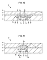
- Fig. 10 is a sectional view of an illumination device according to a sixth embodiment of the present invention.
- the illumination device 1A of the light radially irradiated from the bare chip (light emitting element) 6, the light directed to the side is reflected on the side wall of the recess portion 2a to reach the light guide layer 4 owing to the narrow opening area of the recess portion 2a. Such light becomes the stray light which may cause the hot spot.
- An illumination device 1I as the sixth embodiment includes plural stepped portions having the opening area gradually widened from the deepest position to the upper surface.
- the illumination device 1I according to the sixth embodiment may increase the amount of the light directly guided from the bare chip (light emitting element) 6 into the light guide layer 4. This may prevent generation of the hot spot, thus allowing the surface of the light guide layer 4 to be uniformly illuminated.
- the recess portion 2a with the plural stepped portions is applicable to the other embodiments.
- the wires 8a, 8b may be wire bonded to the conductive patterns 7a, 7b formed on the bottom of the recess portion 2a, or may be wire bonded to conductive patterns 7a', 7b' formed on the respective stepped portions 2b, 2b.
- Fig. 11 is a sectional view of an illumination device according to a seventh embodiment of the present invention.
- An illumination device 1J according to the seventh embodiment shown in Fig. 11 includes a raised sealant 9 for sealing the bare chip 6 in the recess portion 2a, having a surface 9a formed into a convex shape, preferably, a spherical surface.
- the resin film for forming the light guide layer 4 may be formed of a transparent material or a semi-transparent material which contains a light diffusion layer, and is adhered and fixed to the surface 9a of the raised sealant 9 and the surface of the substrate 2 via the adhesive layer 3.
- the surface 9a of the sealant 9 has the convex shape, and accordingly, the interface between the adhesive layer 3 and the light guide layer 4 for covering the surface has the convex shape. Then the incident angle of the light output from the light source (bare chip 6) into the interface between the adhesive layer 3 and the light guide layer 4 becomes smaller than the incident angle of the light into the interface with the shape other than the convex (for example, flat or concave shape). This may improve the transmittance to allow more light output from the bare chip 6 to be guided to the light guide layer 4.
- the illumination device 1J is capable of performing brighter illumination.
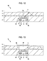
- Fig. 12 is a sectional view of an illumination device according to an eighth embodiment of the present invention.
- Fig. 13 is a sectional view of an illumination device as a modified example of the eighth embodiment.
- an illumination device 1K has a portion of the adhesive layer 3 opposite the recess portion 2a and positioned between the upper surface of the sealant 9 and the lower surface of the light guide layer 4 removed, or the adhesive layer 3 is not formed at the section expected to form the air layer 5a beforehand.
- the illumination device 1K the light emitted from the bare chip 6 transmits from the sealant 9 to pass the air layer 5a so as to be guided to the light guide layer 4.
- the illumination device may be provided with the flat mirror member 11 as described above, and the mirror member 11 with the tapered reflection surface 11a on the surface of the light guide layer 4 opposite the recess portion 2a as indicated by the dotted line.
- An illumination device 1L as a modified example of the eighth embodiment includes an opening 4b to form an air layer 5b by eliminating the adhesive layer 3 and the light guide layer 4 opposite the recess portion 2a, or preventing formation of the adhesive layer 3 and the light guide layer 4 in the corresponding section.
- the mirror member 11 is disposed above the opening 4b to close the air layer 5b.
- the mirror member 11 may be provided with a tapered reflection surface 11a (see Fig. 3 ).
- the illumination device 1J the light emitted from the bare chip 6 passes from the sealant 9 to the air layer 5b so as to be guided into the light guide layer 4. Alternatively, the light reflects on the mirror member 11 once, and then is guided into the light guide layer 4.
- the light advances along the path from the light source (bare chip 6), the sealant 9, the air layer 5a or 5b, the light guide layer 4 to the air layer 5 sequentially.
- the section with different absolute refractive index is provided on the path where the light passes before it leaks out (air layer 5) of the light guide layer 4 so as to propagate the light while being widely diffused. This makes it possible to illuminate the entire light guide layer 4 brightly.
- the light guide layer 4 in the eighth embodiment and the modified example may be the transparent resin film, or the semi-transparent resin film.
- Fig. 14 is a sectional view of an illumination device according to a ninth embodiment.
- Fig. 15 is a sectional view of an illumination device as a modified example of the ninth embodiment.
- An illumination device 1M includes an opening 4b above the recess portion 2a, and a light guide member 20 in the opening 4b.
- the light guide member 20 includes an incident surface 20A to which the light is irradiated from the bare chip 6 as shown in the lower surface of the drawing (surface at Z2 side shown in Fig. 14 ), and an ejection surface (side surface) 20B on the outer circumference (side direction) of the region between the upper and the lower surfaces, from where the incident light ejects toward the light guide layer 4.
- the lower surface of the light guide member 20 is directed opposite the bare chip 6, and the ejection surface (side surface) 20B of the light guide member 20 is directed opposite the inner surface 4c of the light guide layer.
- the single transparent or semi-transparent light guide resin layer may be employed for forming the light guide member 20.
- plural light guide resin layers each with different absolute refractive index may be laminated to form the single light guide member 20.
- An incident angle ⁇ 2 with respect to the boundary surface between the light guide member 20 and the air layer 5 may be made larger than a critical angle ⁇ c between the aforementioned angles to allow the full reflection.
- the amount of light which leaks from the upper surface 20C of the light guide member 20 above the recess portion 2a or right above the bare chip 6 may be reduced.
- the amount of light which transmits from an ejection surface 20B as the side surface of the light guide member 20 to the inner surface 4c of the light guide layer 4 may be increased.
- the incident angle ⁇ 2 at the boundary surface between the light guide member 20 and the air layer 5, and a reflection angle ⁇ 2' thereof may be increased.
- the incident angle ⁇ 3 at the boundary surface between the light guide layer 4 and the adhesive layer 3, and a reflection angle ⁇ 3' thereof may be increased. This makes it possible to propagate the light which passes inside the light guide layer 4 to the further location.
- the light guide member 20 formed by laminating plural light guide resin layers it is preferable to laminate those layers to have the absolute refractive index values gradually increased from the lower surface (surface at the Z2 side) to the upper surface (surface at the Z1 side) of the light guide member 20.
- the refraction angles of the respective light guide resin layers may be gradually decreased such that the incident angle ⁇ 2 of the light directed to the boundary surface between the light guide member 20 and the air layer 5 is made larger than the critical angle ⁇ c on the boundary surface.
- the light guide member 21 is formed as a three-layer structure including an upper clad layer 21a, a core layer 21b and a lower clad layer 21 c.
- the lower clad layer 21c may be designed to serve as the adhesive layer.
- the absolute refractive index of the core layer 21b for forming the light guide member 21 is higher than each absolute refractive index of the upper clad layer 21a and the lower clad layer 21c.
- the light passing inside the core layer 21 b enters into the respective boundary surfaces between the core layer 21b and the upper/lower clad layers 21a, 21c at the incident angle equal to or larger than the critical angle. The light is, thus, allowed to advance farther away while being fully reflected on the boundary surface.
- Fig. 16 is a sectional view of an illumination device according to a tenth embodiment of the present invention.
- the surface 9a of the sealant 9 inside the recess portion 2a is formed into a convex shape, more preferably, a spherical shape, and a light guide member 22 is provided above the surface 9a. That is, a concave surface 22d corresponding to the surface 9a is formed in the lower surface of the core layer 22b for forming the light guide member 22, and the space between the concave curved surface 22d and the surface 9a of the sealant 9 is fixed with the lower clad layer 22c serving as the adhesive layer. Likewise the aforementioned structure, respective values of the absolute refractive index of the upper clad layer 22a and the lower clad layer 22c are smaller than the refractive index of the core layer 22b.
- the incident angle of the light output from the light source into the surface 9a of the sealant 9 becomes small.
- most of the light output from the bare chip 6 may be guided to the light guide layer 4.
- the modified example of the ninth embodiment shown in Fig. 15 the light passing inside the light guide layer 4 is allowed to advance farther away while being fully reflected on the boundary surface.
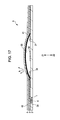
- FIG. 17 to 19 is a sectional view showing a portion of an input device installed in a mobile terminal device as an example which employs the illumination device.
- Each of input devices A to C shown in Figs. 17 to 19 includes a metal dome switch (switch mechanism) 30 and any one of the above-described illumination devices 1.
- a ring-shaped connector electrode 31 is formed on the surface of the substrate 2, and a counter electrode 32 separated from the connector electrode 31 is formed on the center thereof.
- a reversing member 33 formed of a dome-like metal plate is provided. A proximal end of the reversing member 33 at the circumferential side is conductive connected to the surface of the connector electrode 31.
- the reversing member 33 deforms to bring the metal plate at its back side into contact with the counter electrode 32.
- the connector electrode 31 and the counter electrode 32 are conductive connected via the reversing member 33. That is, the connector electrode 31, the counter electrode 32 and the reversing member 33 form the metal dome switch (switch mechanism) 30 which is capable of switching ON/OFF between the connector electrode 31 and the counter electrode 32 based on the pressurized state.
- the light guide layer 4 as the transparent or the semi-transparent resin film is laminated on the surfaces of the substrate 2 and the reversing member 33.
- the light guide layer 4 is tightly fixed to the surfaces of the substrate 2 and the reversing member 33 via the adhesive layer 3 therebetween.
- a light emitting element as the bare chip 6 is buried in the recess portion 2a of the substrate 2, around which is filled with the sealant 9.
- the upper portion of the light guide layer 4 is covered with a casing 40 for forming an outer case of the mobile terminal device.
- the dome-like reversing member 33 is exposed outside through an opening 41 formed in the casing 40. The light which has leaked from the light guide layer 4 never leaks outside the casing 40 from the area other than the opening 41.
- the light emitted from the bare chip 6 passes inside the light guide layer 4 while fully reflecting.
- the light propagating in the light guide layer 4 impinges against the proximal end of the reversing member 33 to have the direction changed to the one along the dome shape for forming the reversing member 33.
- reflection and scattering of the light occurs around the proximal end.
- the resultant light leaks out of the casing 40 via the opening 41. This makes it possible to illuminate the region around the proximal end of the reversing member 33 brighter than any other region.
- an optical element 50 formed of a scattering substance or fluorescent substance is disposed around the metal dome switch 30.
- the optical element 50 is fixed onto the substrate 2, and exposed outside the casing 40 through a hole 42 formed in the casing 40 around the metal dome switch 30.
- the optical elements 50 may be distributed around the metal dome switch 30.
- the optical element 50 is disposed opposite the inner surface of a mount hole 4A formed in the light guide layer 4.
- the light propagating inside the light guide layer 4 leaks from the inner surface of the mount hole 4A so as to be irradiated to the optical element 50.
- light scattering occurs in the scattering substance, or the specific wavelength of the light irradiated from the light guide layer 4 is absorbed by the fluorescent substance so as to yield a fluorescence to generate the visible light.
- the region around the metal dome switch 30, thus, may be brightly illuminated.
- a triangular prism is disposed as the optical element 50 instead of the scattering substance or the fluorescent substance as described in the second example.
- the light leaking from the inner surface of the mount hole 4A is irradiated to the triangular prism to scatter the light.
- the triangular prism is formed of the transparent resin, and the filler is mixed with the inside portion of the resin so as to form the optical element for facilitating the diffused reflection of the light inside.
- the use of the illumination device 1 according to the present invention allows the metal dome switch 30 installed in any of the input devices A to C of the mobile terminal device and the circumference thereof to be brightly illuminated. This makes it possible to improve the operability of the mobile terminal device.
- the optical element 50 is disposed opposite the inner surface of the mount hole 4A formed in the light guide layer 4.
- the present invention is not limited to the structure as described above.
- the optical element 50 may have its bottom (incident surface) fixed while being directed to the surface of the light guide layer 4 so as to scatter or yield the fluorescence with respect to the light leaking from the surface of the light guide layer 4.
Landscapes
- Physics & Mathematics (AREA)
- General Physics & Mathematics (AREA)
- Optics & Photonics (AREA)
- Planar Illumination Modules (AREA)
- Push-Button Switches (AREA)
- Light Guides In General And Applications Therefor (AREA)
- Switch Cases, Indication, And Locking (AREA)
Abstract
[Object] To provide a thin illumination device capable of efficiently utilizing light emitted from a light source, and an input device equipped with the illumination device.
[Means for Solution] A recess portion 2a is formed in a substrate 2 to accommodate a light emitting element 6 so as to be sealed with a sealant 9. A light guide layer 4 formed of a thin transparent resin film is fixed onto the substrate 2 via an adhesive layer 3 to realize an illuminating device 1A with a thin structure. The light emitted from the light emitting element 6 is irradiated into the light guide layer 4 via the sealant 9 and the adhesive layer 3. The light fully reflecting on the boundary surfaces between the light guide layer 4 and the adhesive layer 3, and between the light guide layer 4 and the air layer 5 passes inside the light guide layer 4. Then the light which has not fully reflected leaks outside from the surface of the transparent resin film which forms the light guide layer 4. This makes it possible to illuminate the surface of the illumination device 1A entirely with brightness.
Description
- The present invention relates to an illumination device for illuminating an operation unit for various types of electronic devices, and more particularly, to a thin illumination device capable of effectively utilizing the light emitted from a light source, and an input device equipped with the illumination device.
- An electronic device of such type as audio equipment and a mobile electronic device is provided with a light guide member for guiding the light emitted from the light source such as the LED to the operation surface so as to illuminate the operation button, the fixed letter marked on the operation surface and the display unit having numbers displayed thereon.
- Generally, the illumination device of the aforementioned type is structured to allow an illumination member such as an acrylic sheet attached to the back side of the operation surface of the electronic device to guide the light from the light source. This structure needs the space on the back side of the operation surface for accommodating the illumination member, which hinders the electronic device from having the thin structure.
-
Patent Document 1 discloses a laminated sheet for an optical element having an LED disposed in a recess portion formed in abonding sheet 2 above thecore material 1, and having the LED sealed with a transparent synthetic resin (light guide member).
Patent Document 1: Japanese Unexamined Patent Application Publication No.2003-86847 - In the generally employed illumination device as disclosed in
Patent Document 1, the refractive index of the light guide member as an emission source is larger than that of an air layer as an emission target. The incident light at the incident angle smaller than the critical angle from those emitted from the light source such as the LED transmits the light guide member to be lost. In the generally employed illumination device, the incident light partially leaks without being reflected in the light guide member, resulting in the low light utilization efficiency. For this reason, the light source with unnecessarily large output has to be used, or the number of the light sources has to be increased. - With the generally employed illumination device, the area surrounding the light source is brightly illuminated. However, it is likely to become darker as the target is remote from the light source, resulting in the problem of the large illuminance difference.
- The use of the generally employed illumination device may form island-like brighter spots (hot spot) on the surface of the light guide layer through scattering of the stray light, which may fail to uniformly illuminate the light guide layer surface.
- It is an object of the present invention to provide an illumination device with the thin structure, and an input device equipped with the illumination device.
- It is another object of the present invention to provide an illumination device capable of improving light utilization efficiency and supplying highly uniform bright illumination, and an input device equipped with the illumination device.
- The present invention provides an illumination device which includes a substrate with a recess portion formed in a surface, a light emitting element installed in the recess portion, and a light guide layer laminated on a surface of the substrate. The light guide layer formed of a thin resin film and the surface of the substrate are fixed via an adhesive layer therebetween.
- In the present invention, a resin film is used as the light guide layer, and the resin film is directly fixed to the substrate via the adhesive layer, thus simplifying and thinning the structure of the illumination device.
- Preferably, an absolute refractive index of the adhesive layer is smaller than an absolute refractive index of the resin film.
- In the structure, one surface (incident surface) of the resin film which forms the light guide layer is in contact with the adhesive layer, and the other surface is in contact with an air layer. Each absolute refractive index of the adhesive layer and the air layer is smaller than that of the resin film. So the resin film serves as a light guide path for propagating the light which fully reflects among the light rays passing therethrough.
- Preferably, a sealant is filled in the recess portion to seal the light emitting element.
- A
bare chip 6 may be protected by the structure. - Preferably, a surface of the sealant is raised to have a convex shape, and a surface of the sealant and the light guide layer are bonded with the adhesive layer therebetween.
- In the aforementioned structure, the incident angle at which the light output from the light source is irradiated to the interface between the adhesive layer and the light guide layer becomes small. The transmittance at the interface is improved so as to guide more light output from the light source to the light guide layer.
- In the structure, a reflection recess portion is formed in the surface of the light guide layer opposite the light emitting element. The reflection recess portion is tapered from the surface to the inside of the light guide layer.
- In the structure, the inclined surface of the reflection recess portion may be used as the reflection surface, thus guiding the light to the light guide layer efficiently.
- For example, the reflection recess portion is in the form of an inclined surface which forms a V-like cross section, or a meniscus portion.
- Preferably, a mirror member or a light absorbing member is disposed on the surface of the light guide layer at the position opposite at least the light emitting element.
- When the mirror member is employed, the structure ensures to reflect the light that is about to transmit the light guide layer so as to be guided thereto. When the light absorbing member is employed, the structure is capable of preventing generation of the island-like hot spots.
- Preferably, the mirror member includes a tapered reflection surface.
- The structure allows the light to be propagated to the location far away from the light source.
- Preferably, the resin film is transparent or semi-transparent. For example, the light guide layer may be formed by laminating a transparent resin film and a semi-transparent resin film.
- The aforementioned structure allows the light to be scattered, resulting in the highly uniform illumination.
- Preferably, the recess portion of the substrate is formed of a stepped portion having an opening area gradually increased from a deepest portion toward a surface of the recess portion.
- The structure may increase the amount of light directly irradiated from the light source to the light guide layer. As the incident angle of the newly irradiated light is large, the light may be propagated to the location further away.
- Preferably, the adhesive layer is not formed in a section opposite the light emitting element, and an air layer is formed in a section adjacent to the light guide layer and the light emitting element.
- The structure is capable of propagating the light while being widely diffused, thus illuminating the entire light guide layer with sufficient brightness.
- Preferably, an opening is formed in a surface of the substrate on which the light guide layer is laminated at the position opposite the recess portion by partially removing the light guide layer. A light guide member is formed inside the opening, having opposite upper and lower surfaces and a side surface interposed therebetween to form an outer circumferential portion. The lower surface is disposed opposite the light emitting element, and the inner surface of the opening is disposed opposite the side surface of the light guide member.
- The structure takes the light emitted from the light emitting element from the lower surface of the light guide member so as to guide the light to the light guide layer via the side surface of the light guide member.
- Preferably, the light guide member is formed by laminating a lower clad layer, a core layer and an upper clad layer from the bottom, and an absolute refractive index of the core layer is higher than each absolute refractive index of the lower and the upper clad layers.
- The structure is capable of increasing the refraction angle upon incidence of the light to the light guide member to make sure to propagate the light to the location further away.
- The present invention provides an input device using the illumination device as any one of those described above. The substrate includes a switch mechanism provided with a reversibly mounted metal reversing member and a counter electrode disposed opposite the reversing member. A surface of the reversing member is covered with the light guide layer.
- The input device according to the present invention is capable of illuminating the switch mechanism using the illumination device. In the aforementioned structure, preferably, an optical element for scattering light or yielding a fluorescence is disposed in at least a portion of the light guide layer. For example, the optical element is any one of a scattering substance, a fluorescent substance and a prism.
- The structure allows the use of various types of light to illuminate the switch mechanism.
- Preferably, the optical element is disposed around the switch mechanism.
- The structure is capable of illuminating the area around the switch mechanism without being illuminated directly. The same effect as the one derived from direct illumination of the switch mechanism may be obtained.
- The present invention is capable of preventing the light loss in the light guide member, resulting in the improved light utilization efficiency. The member to be illuminated (switch mechanism), thus may be illuminated more brightly. The present invention is capable of making manufacturing of the illumination device easier, and forming the thin structure.
-
Fig. 1 is a sectional view of an illumination device according to a first embodiment of the present invention.Fig. 1 graphically shows the light passing in the light guide layer with an arrow mark, which applies to the subsequent embodiments. - Referring to
Fig. 1 , anillumination device 1A includes asubstrate 2 which may be the synthetic resin substrate that does not substantially deflect, the film-like synthetic resin substrate that can easily deflect, or the metal substrate. - The
substrate 2 has arecess portion 2a formed in the surface, and a bare chip (light source) 6 as an optical element accommodated to be fixed in therecess portion 2a with the adhesive agent. Electrode layers of thebare chip 6 are individually coupled (wire bonding) withconductive patterns recess portion 2a via thinconductive wires sealant 9 formed of the clear synthetic resin is filled in therecess portion 2a so as to seal thebare chip 6 and thewires bare chip 6, and to further prevent the failure such as disconnection of thewires - The
bare chip 6 may be structured to output the light in any color of red, green or blue. Alternatively, the light in other color, for example, white may be output. In case of the red light emission, the emission peak wavelength may be in the range from 610 to 740 nm. If thebare chip 6 is of the type for emitting green light, the emission peak wavelength may be in the range from 500 to 565 nm. If thebare chip 6 is of the type for emitting blue light, the emission peak wavelength may be in the range from 430 to 485 nm. - An
adhesive layer 3 is formed on the surface of thesubstrate 2, and alight guide layer 4 is further formed on theadhesive layer 3. The surface of thelight guide layer 4 is kept in contact with a space as anair layer 5. - The
light guide layer 4 is formed of a thin film with a thickness preferably in the range from 10 to 100 µm, and more preferably in the range from 60 to 80 µm in consideration of the need for controlling the shape of the light guide layer and reducing the thickness. Thelight guide layer 4 is formed of a PET (polyethylene terephthalate) resin film, a PMMA (polymethylmethacrylate) resin film, a TAC (triacetylcellulose) resin film, an epoxy-based resin film with high refractive index, a silicone series resin film, and a translucent resin film such as a phenol-based resin film and an acrylic resin film. The light transmission rate of the aforementioned translucent resin film which forms thelight guide layer 4 is 95% or higher. It can be said that the aforementioned film is substantially a transparent resin film. - The
adhesive layer 3 is formed of a transparent acrylic adhesive agent or fluorine-contained epoxy-based adhesive agent. - Preferably, the absolute refractive index value of the
sealant 9 is similar to that of theadhesive layer 3. The absolute refractive index value of thelight guide layer 4 is higher than each value of theadhesive layer 3 and theair layer 5. The absolute refractive index of theadhesive layer 3 is higher than that of air. Most of the light emitted from thebare chip 6 transmits thesealant 9 and theadhesive layer 3 to be guided to thelight guide layer 4. A portion of the aforementioned light passes in thelight guide layer 4 while fully reflecting on the boundary surface between thelight guide layer 4 and theadhesive layer 3, and the boundary surface between thelight guide layer 4 and theair layer 5. The portion of the light which does not fully reflect leaks outside from the surface of the transparent resin film that forms thelight guide layer 4. Accordingly, theillumination device 1A serves as the surface-emitting structure. - The
illumination device 1A of the first embodiment employs the thin transparent resin film for forming thelight guide layer 4 so as to be bonded to thesubstrate 2 via the thinadhesive layer 3, thus simplifying the manufacturing process and reducing the thickness of the entire structure. -
Fig. 2 is a sectional view of an illumination device according to a second embodiment of the present invention.Fig. 3 is a sectional view of a modified example of the second embodiment. Hereinafter, the same components as those described in the above embodiments will be designated with the same reference numerals. - An
illumination device 1 B according to the second embodiment shown inFig. 2 has substantially the same structure as that of theillumination device 1A according to the first embodiment except that amirror member 11 is disposed on the surface of thelight guide layer 4 above the recess portion 1a at the position opposite thebare chip 6. - In the embodiment, of the light directly irradiated into the
light guide layer 4 from thebare chip 6, the light which has transmitted through thelight guide layer 4 via the position above the recess portion 1a reflects on themirror member 11 so as to be returned into thelight guide layer 4. The structure of the embodiment prevents leakage of the light irradiated to the boundary surface between thelight guide layer 4 and theair layer 5 at the incident angle smaller than the critical angle, which is supposed to leak out of thelight guide layer 4. Of the light directly irradiated into thelight guide layer 4 from thebare chip 6, the amount of the light that directly leaks outside thelight guide layer 4 above the recess portion 1a without reflection may be suppressed. This makes it possible to increase the amount of the light propagated through thelight guide layer 4, and to irradiate more light to the location further away from thebare chip 6. In theillumination device 1A according to the first embodiment, the center region opposite thebare chip 6 is illuminated with the highest luminance, and the luminance is gradually lost as the light is directed to the circumferential location far away from thebare chip 6, resulting in large difference in the light intensity between the center and the circumferential location. - The
illumination device 1 B of the second embodiment prevents the leakage of the light at the center opposite thebare chip 6, which allows more light to be guided to the circumferential location. Accordingly, the difference in the light intensity between the center and the circumferential location may be reduced. That is, theillumination device 1 B may be of surface-emitting type for uniform emission. - An
illumination device 1C shown inFig. 3 as the modified example of the second embodiment shown inFig. 2 has the similar structure to theillumination device 1 B except that the lower surface (reflection surface) of themirror member 11 has taperedsurfaces - In the modified example shown in
Fig. 3 , of the light irradiated directly from thebare chip 6 into thelight guide layer 4, the light irradiated at the small incident angle θ1 with respect to the axis perpendicular to the boundary surface between theadhesive layer 3 and thelight guide layer 4 is allowed to reflect on thereflection surface 11a at the large reflection angle θ2. This makes it possible to increase the angle (reflection angle θ3 at the boundary surface with theadhesive agent 3, and the reflection angle θ4 at the boundary surface between thelight guide layer 4 and the air layer 5) at which the light reflects in thelight guide layer 4 subsequently. This makes it possible to propagate the light from thebare chip 6 at the center to the remote location. Theillumination device 1C provides the wide emission area. -
Fig. 4 is a sectional view of an illumination device according to a third embodiment of the present invention. - An
illumination device 1 D shown inFig. 4 has substantially the same structure as that of the illumination device according to the second embodiment except that alight absorbing member 12 is disposed on the surface of thelight guide layer 4 above the position opposite therecess portion 2a or thebare chip 6 instead of themirror member 11. - The
light absorbing member 12 may be formed as a black layer with uniformity. In this case, however, a large amount of light is absorbed, which may require more outputs of the light source (bare chip 6) for providing sufficient light to serve as the illumination device, thus deteriorating the efficiency. It is preferable to form the black dot pattern or black matrix pattern on thelight absorbing member 12 so as to allow a part of the light to transmit therethrough. Such member may be obtained by forming a metal chrome film on the glass substrate through spattering to be finished into the dot or the matrix pattern through the photolithography. Alternatively, the thin metal film (chrome, nickel, aluminum in the form of an elementary substance, an alloy or an oxide) is deposited or spattered on the surface of the light guide layer at the air side using the same principle as the case of ND filter to allow the part of the light to absorb or reflect, and the rest of the light to transmit. The thus formedlight absorbing member 12 is fixed on the surface of thelight guide layer 4 above therecess portion 2a. - In the embodiment, of the light irradiated into the
light guide layer 4 from thebare chip 6, the light scattered on the concavo-convex surfaces of theadhesive layer 3 and the concavo-convex upper and lower surfaces of thelight guide layer 4 on the transmission path may be absorbed by thelight absorbing member 12. This makes it possible to suppress generation of the island-like pattern of the plural brighter spots (hot spot) caused by scattering of stray light, which may enevenly illuminate the surface of thelight guide layer 4. -
Fig. 5 is a sectional view of an illumination device according to a fourth embodiment of the present invention. - An
illumination device 1 E shown inFig. 5 has substantially the same structure as that of the illumination device of the first embodiment except that areflection recess portion 4a is formed in the surface of thelight guide layer 4 at the position opposite therecess portion 2a or thebare chip 6, which is tapered from the surface inward. - The
reflection recess portion 4a has a substantially V-like cross section which allows inclined surfaces 4a1 forming the V-shape to serve as the reflection mirror. Theillumination device 1 E according to the fourth embodiment is capable of guiding the light directly irradiated to thelight guide layer 4 from thebare chip 6 into thelight guide layer 4 by the reflection on the inclined surface 4a1. Unlike the case without thereflection recess portion 4a where a part of the light directly irradiated from thebare chip 6 to thelight guide layer 4 transmits therethrough to be lost, the embodiment is capable of preventing the aforementioned leakage of the light. Likewise the fourth embodiment, the incident angle of the light at the subsequent reflection in the light guide layer 4 (reflection angle on the boundary surface between thelight guide layer 4 and theadhesive layer 3, and the reflection angle on the boundary surface between thelight guide layer 4 and the air layer 5) may be increased. This makes it possible to propagate the light to the location further away from thebare chip 6. Theillumination device 1 E with a wide emission range may be provided. -
Fig. 6 is a sectional view of an illumination device according to a fourth embodiment of the present invention.Fig. 7 is an enlarged sectional view representing a portion of the illumination device shown inFig. 6 .Fig. 8 is a sectional view showing a modified example of the illumination device of the fourth embodiment. - In the fourth embodiment shown in
Fig. 6 , the portion of thelight guide layer 4, which is opposite therecess portion 2a has anopening 4b, aninner surface 4c of which is provided with a meniscus portion (reflection recess portion) 13 as a quadratic function curve having a concave cross section. - The
meniscus portion 13 is formed in theillumination device 1A (seeFig. 1 ) having thelight guide layer 4 formed of the resin film bonded onto thesubstrate 2 via theadhesive layer 3. That is, theopening 4b is formed by removing thelight guide layer 4 and theadhesive layer 3 for forming the circular part in the exposure/development process. When a small amount of the liquid synthetic resin in the molten state is poured into theopening 4b, the circumferential portion of the liquid synthetic resin is raised at the level higher than the center through the capillary phenomenon. In the aforementioned state, the liquid synthetic resin is cured to form themeniscus portion 13. - The light irradiated from the
bare chip 6 refracts on the boundary between thesealant 9 and themeniscus portion 13, reflects on the boundary surface between arecess surface 13a of themeniscus portion 13 and theair layer 5, and further refracts on the boundary between themeniscus portion 13 and theinner surface 4c of thelight guide layer 4 so as to be guided into thelight guide layer 4. This makes it possible to guide more light to thelight guide layer 4. - Preferably, the full reflection on the boundary surface between the
recess surface 13a of themeniscus portion 13 and theair layer 5 reduces the amount of light that transmits from therecess surface 13a to theair layer 5. As the enlarged view ofFig. 7 shows, it is preferable to set an incident angle α1 with respect to the axis perpendicular to the boundary surface (tangential line) L1 between therecess surface 13a of themeniscus portion 13 and theair layer 5 to be equal to or larger than the critical angle θc with respect to the boundary surface L1. Preferably, the synthetic resin for forming themeniscus portion 13 has the absolute refractive index n13 equal to or smaller than the absolute refractive index n9 of the resin for forming thesealant 9 such that the refraction angle α2 of the light irradiated from thesealant 9 to themeniscus portion 13 becomes large. - Preferably, a large amount of light passes without fully reflecting on the boundary between the
meniscus portion 13 and the inner surface 4C of thelight guide layer 4. It is preferable to set the absolute refractive index n13 of the synthetic resin for forming themeniscus portion 13 to be equal to or smaller than the absolute refractive index n4 of the resin film for forming thelight guide layer 4. Preferably, the absolute refractive index values of n9, n13 and n4 of the synthetic resins for forming thesealant 9 and themeniscus portion 13, and the resin film for forming thelight guide layer 4 establish the relation of n13≤n9≤n4. - An
illumination device 1F according to the fourth embodiment reflects the light irradiated to therecess surface 13a of themeniscus portion 13 so as to be guided into thelight guide layer 4 via theinner surface 4c thereof. However, it is difficult to guide the light irradiated to the area around the bottom of therecess surface 13a into thelight guide layer 4. - An
illumination device 1G as a modified example shown inFig. 8 is formed by providing themirror member 11 on the surface of thelight guide layer 4 right above theopening 4b having themeniscus portion 13 of theillumination device 1F shown inFig. 6 . - In the
illumination device 1G, the incident light at the area around the bottom of therecess surface 13a of themeniscus portion 13 transmits inside theopening 4b to reflect on themirror member 11 so as to be guided to theinner surface 4c of thelight guide layer 4. Likewise theillumination device 1B (seeFig. 2 ) according to the second embodiment, the illumination device ensures to guide the light reflecting on themirror member 11 into thelight guide layer 4. - The
mirror member 11 may have taperedreflection surfaces Fig. 3 ). Besides themirror member 11, thelight absorbing member 12 shown in theillumination device 1 D (seeFig. 4 ) according to the third embodiment may be employed to suppress generation of the hot spot on the surface of thelight guide layer 4. -
Fig. 9 is a sectional view of an illumination device according to a fifth embodiment of the present invention. - In an
illumination device 1 H shown inFig. 9 , the filler is mixed with the inside of the transparent resin for forming thelight guide layer 4 to form a light scattering layer for diffusely reflecting the light therein. The filler may be formed as white inorganic oxide powder, metal powder and the like. The resin film is semi-transparent. The filler may be mixed with the adhesive agent for forming theadhesive layer 3 instead of mixing the filler with thelight guide layer 4 so as to form the semi-transparentadhesive layer 3 as the light scattering layer. - The resin film (light scattering layer) formed by mixing the filler may be laminated on at least one of the upper and the lower surfaces of the transparent resin film to form the
light guide layer 4. - The
illumination device 1 H according to the fifth embodiment is capable of enhancing the optical diffusion in the light scattering layer which contains the filler, resulting in the uniform illumination with less unevenness. - The structure according to the first to the fourth embodiments may include the
light guide layer 4 as described in the fifth embodiment instead of the transparentlight guide layer 4. -
Fig. 10 is a sectional view of an illumination device according to a sixth embodiment of the present invention. - In the case of the
illumination device 1A according to the first embodiment, of the light radially irradiated from the bare chip (light emitting element) 6, the light directed to the side is reflected on the side wall of therecess portion 2a to reach thelight guide layer 4 owing to the narrow opening area of therecess portion 2a. Such light becomes the stray light which may cause the hot spot. - An illumination device 1I as the sixth embodiment includes plural stepped portions having the opening area gradually widened from the deepest position to the upper surface. The illumination device 1I according to the sixth embodiment may increase the amount of the light directly guided from the bare chip (light emitting element) 6 into the
light guide layer 4. This may prevent generation of the hot spot, thus allowing the surface of thelight guide layer 4 to be uniformly illuminated. Therecess portion 2a with the plural stepped portions is applicable to the other embodiments. - As a dotted line in
Fig. 10 shows, thewires conductive patterns recess portion 2a, or may be wire bonded toconductive patterns 7a', 7b' formed on the respective steppedportions -
Fig. 11 is a sectional view of an illumination device according to a seventh embodiment of the present invention. - An
illumination device 1J according to the seventh embodiment shown inFig. 11 includes a raisedsealant 9 for sealing thebare chip 6 in therecess portion 2a, having asurface 9a formed into a convex shape, preferably, a spherical surface. The resin film for forming thelight guide layer 4 may be formed of a transparent material or a semi-transparent material which contains a light diffusion layer, and is adhered and fixed to thesurface 9a of the raisedsealant 9 and the surface of thesubstrate 2 via theadhesive layer 3. - In the
illumination device 1J according to the seventh embodiment, thesurface 9a of thesealant 9 has the convex shape, and accordingly, the interface between theadhesive layer 3 and thelight guide layer 4 for covering the surface has the convex shape. Then the incident angle of the light output from the light source (bare chip 6) into the interface between theadhesive layer 3 and thelight guide layer 4 becomes smaller than the incident angle of the light into the interface with the shape other than the convex (for example, flat or concave shape). This may improve the transmittance to allow more light output from thebare chip 6 to be guided to thelight guide layer 4. Especially when thesealant 9 has substantially the same absolute refractive index as that of theadhesive layer 3, the reflection of the light on the interface between thesealant 9 and theadhesive layer 3 may be suppressed. This makes it possible to transmit most of the light directed from thesealant 9 to theadhesive layer 3, thus enhancing the light utilization efficiency. That is, theillumination device 1J is capable of performing brighter illumination. -
Fig. 12 is a sectional view of an illumination device according to an eighth embodiment of the present invention.Fig. 13 is a sectional view of an illumination device as a modified example of the eighth embodiment. - Referring to
Fig. 12 , anillumination device 1K according to the eighth embodiment has a portion of theadhesive layer 3 opposite therecess portion 2a and positioned between the upper surface of thesealant 9 and the lower surface of thelight guide layer 4 removed, or theadhesive layer 3 is not formed at the section expected to form theair layer 5a beforehand. In theillumination device 1K, the light emitted from thebare chip 6 transmits from thesealant 9 to pass theair layer 5a so as to be guided to thelight guide layer 4. Referring toFig. 12 , the illumination device may be provided with theflat mirror member 11 as described above, and themirror member 11 with the taperedreflection surface 11a on the surface of thelight guide layer 4 opposite therecess portion 2a as indicated by the dotted line. - An
illumination device 1L as a modified example of the eighth embodiment includes anopening 4b to form anair layer 5b by eliminating theadhesive layer 3 and thelight guide layer 4 opposite therecess portion 2a, or preventing formation of theadhesive layer 3 and thelight guide layer 4 in the corresponding section. Themirror member 11 is disposed above theopening 4b to close theair layer 5b. Themirror member 11 may be provided with a taperedreflection surface 11a (seeFig. 3 ). In theillumination device 1J, the light emitted from thebare chip 6 passes from thesealant 9 to theair layer 5b so as to be guided into thelight guide layer 4. Alternatively, the light reflects on themirror member 11 once, and then is guided into thelight guide layer 4. - In the eighth embodiment shown in
Fig. 12 and the modified example shown inFig. 13 , the light advances along the path from the light source (bare chip 6), thesealant 9, theair layer light guide layer 4 to theair layer 5 sequentially. The section with different absolute refractive index is provided on the path where the light passes before it leaks out (air layer 5) of thelight guide layer 4 so as to propagate the light while being widely diffused. This makes it possible to illuminate the entirelight guide layer 4 brightly. - The
light guide layer 4 in the eighth embodiment and the modified example may be the transparent resin film, or the semi-transparent resin film. -
Fig. 14 is a sectional view of an illumination device according to a ninth embodiment.Fig. 15 is a sectional view of an illumination device as a modified example of the ninth embodiment. - An
illumination device 1M according to the ninth embodiment shown inFig. 14 includes anopening 4b above therecess portion 2a, and alight guide member 20 in theopening 4b. Thelight guide member 20 includes anincident surface 20A to which the light is irradiated from thebare chip 6 as shown in the lower surface of the drawing (surface at Z2 side shown inFig. 14 ), and an ejection surface (side surface) 20B on the outer circumference (side direction) of the region between the upper and the lower surfaces, from where the incident light ejects toward thelight guide layer 4. The lower surface of thelight guide member 20 is directed opposite thebare chip 6, and the ejection surface (side surface) 20B of thelight guide member 20 is directed opposite theinner surface 4c of the light guide layer. - The single transparent or semi-transparent light guide resin layer may be employed for forming the
light guide member 20. Alternatively, plural light guide resin layers each with different absolute refractive index may be laminated to form the singlelight guide member 20. - In the embodiment, a refraction angle β1 at which the light transmitted through the
sealant 9 from thebare chip 6 and irradiated to an incident surface (lower surface) 20A of thelight guide member 20 becomes large. An incident angle β2 with respect to the boundary surface between thelight guide member 20 and theair layer 5 may be made larger than a critical angle θc between the aforementioned angles to allow the full reflection. The amount of light which leaks from theupper surface 20C of thelight guide member 20 above therecess portion 2a or right above thebare chip 6 may be reduced. The amount of light which transmits from anejection surface 20B as the side surface of thelight guide member 20 to theinner surface 4c of thelight guide layer 4 may be increased. - The incident angle β2 at the boundary surface between the
light guide member 20 and theair layer 5, and a reflection angle β2' thereof may be increased. Likewise, the incident angle β3 at the boundary surface between thelight guide layer 4 and theadhesive layer 3, and a reflection angle β3' thereof may be increased. This makes it possible to propagate the light which passes inside thelight guide layer 4 to the further location. - In the case where the
light guide member 20 formed by laminating plural light guide resin layers, it is preferable to laminate those layers to have the absolute refractive index values gradually increased from the lower surface (surface at the Z2 side) to the upper surface (surface at the Z1 side) of thelight guide member 20. The refraction angles of the respective light guide resin layers may be gradually decreased such that the incident angle β2 of the light directed to the boundary surface between thelight guide member 20 and theair layer 5 is made larger than the critical angle θc on the boundary surface. - In an
illumination device 1 N as the modified example shown inFig. 15 , thelight guide member 21 is formed as a three-layer structure including an upperclad layer 21a, acore layer 21b and a lowerclad layer 21 c. The lowerclad layer 21c may be designed to serve as the adhesive layer. - The absolute refractive index of the
core layer 21b for forming thelight guide member 21 is higher than each absolute refractive index of the upper cladlayer 21a and the lowerclad layer 21c. The light passing inside thecore layer 21 b enters into the respective boundary surfaces between thecore layer 21b and the upper/lowerclad layers -
Fig. 16 is a sectional view of an illumination device according to a tenth embodiment of the present invention. - In an illumination device 1O according to the tenth embodiment, the
surface 9a of thesealant 9 inside therecess portion 2a is formed into a convex shape, more preferably, a spherical shape, and alight guide member 22 is provided above thesurface 9a. That is, aconcave surface 22d corresponding to thesurface 9a is formed in the lower surface of thecore layer 22b for forming thelight guide member 22, and the space between the concavecurved surface 22d and thesurface 9a of thesealant 9 is fixed with the lowerclad layer 22c serving as the adhesive layer. Likewise the aforementioned structure, respective values of the absolute refractive index of the upper cladlayer 22a and the lowerclad layer 22c are smaller than the refractive index of thecore layer 22b. - In the embodiment, the incident angle of the light output from the light source into the
surface 9a of thesealant 9 becomes small. Likewise the seventh embodiment shown inFig. 11 , most of the light output from thebare chip 6 may be guided to thelight guide layer 4. Likewise the modified example of the ninth embodiment shown inFig. 15 , the light passing inside thelight guide layer 4 is allowed to advance farther away while being fully reflected on the boundary surface. - An example using any one of the above-described illumination devices will be described.
- Each of
Figs. 17 to 19 is a sectional view showing a portion of an input device installed in a mobile terminal device as an example which employs the illumination device. Each of input devices A to C shown inFigs. 17 to 19 includes a metal dome switch (switch mechanism) 30 and any one of the above-describedillumination devices 1. - In each of the input devices A to C, a ring-shaped
connector electrode 31 is formed on the surface of thesubstrate 2, and acounter electrode 32 separated from theconnector electrode 31 is formed on the center thereof. A reversingmember 33 formed of a dome-like metal plate is provided. A proximal end of the reversingmember 33 at the circumferential side is conductive connected to the surface of theconnector electrode 31. When the pressure force in the direction Z2 shown in the drawing is applied to the surface of the reversingmember 33, the reversingmember 33 deforms to bring the metal plate at its back side into contact with thecounter electrode 32. As a result, theconnector electrode 31 and thecounter electrode 32 are conductive connected via the reversingmember 33. That is, theconnector electrode 31, thecounter electrode 32 and the reversingmember 33 form the metal dome switch (switch mechanism) 30 which is capable of switching ON/OFF between theconnector electrode 31 and thecounter electrode 32 based on the pressurized state. - In each of the input devices A to C, the
light guide layer 4 as the transparent or the semi-transparent resin film is laminated on the surfaces of thesubstrate 2 and the reversingmember 33. Thelight guide layer 4 is tightly fixed to the surfaces of thesubstrate 2 and the reversingmember 33 via theadhesive layer 3 therebetween. A light emitting element as thebare chip 6 is buried in therecess portion 2a of thesubstrate 2, around which is filled with thesealant 9. - The upper portion of the
light guide layer 4 is covered with acasing 40 for forming an outer case of the mobile terminal device. The dome-like reversingmember 33 is exposed outside through anopening 41 formed in thecasing 40. The light which has leaked from thelight guide layer 4 never leaks outside thecasing 40 from the area other than theopening 41. - In the input device A as the first example shown in
Fig. 17 , the light emitted from thebare chip 6 passes inside thelight guide layer 4 while fully reflecting. The light propagating in thelight guide layer 4 impinges against the proximal end of the reversingmember 33 to have the direction changed to the one along the dome shape for forming the reversingmember 33. At this time, reflection and scattering of the light occurs around the proximal end. As a result, the amount of light which leaks from the region around the proximal end of the reversingmember 33 to the outside thelight guide layer 4 is increased. The resultant light leaks out of thecasing 40 via theopening 41. This makes it possible to illuminate the region around the proximal end of the reversingmember 33 brighter than any other region. - In the input device B as the second example shown in
Fig. 18 , anoptical element 50 formed of a scattering substance or fluorescent substance is disposed around the metal dome switch 30. Theoptical element 50 is fixed onto thesubstrate 2, and exposed outside thecasing 40 through ahole 42 formed in thecasing 40 around the metal dome switch 30. Theoptical elements 50 may be distributed around the metal dome switch 30. - The
optical element 50 is disposed opposite the inner surface of amount hole 4A formed in thelight guide layer 4. The light propagating inside thelight guide layer 4 leaks from the inner surface of themount hole 4A so as to be irradiated to theoptical element 50. In theoptical element 50, light scattering occurs in the scattering substance, or the specific wavelength of the light irradiated from thelight guide layer 4 is absorbed by the fluorescent substance so as to yield a fluorescence to generate the visible light. The region around the metal dome switch 30, thus, may be brightly illuminated. - In the input device C as the third example shown in
Fig. 19 , a triangular prism is disposed as theoptical element 50 instead of the scattering substance or the fluorescent substance as described in the second example. In the example, the light leaking from the inner surface of themount hole 4A is irradiated to the triangular prism to scatter the light. The triangular prism is formed of the transparent resin, and the filler is mixed with the inside portion of the resin so as to form the optical element for facilitating the diffused reflection of the light inside. - In the first to the third examples, the use of the
illumination device 1 according to the present invention allows the metal dome switch 30 installed in any of the input devices A to C of the mobile terminal device and the circumference thereof to be brightly illuminated. This makes it possible to improve the operability of the mobile terminal device. - In the aforementioned examples, the
optical element 50 is disposed opposite the inner surface of themount hole 4A formed in thelight guide layer 4. However, the present invention is not limited to the structure as described above. For example, theoptical element 50 may have its bottom (incident surface) fixed while being directed to the surface of thelight guide layer 4 so as to scatter or yield the fluorescence with respect to the light leaking from the surface of thelight guide layer 4. -
- [
Fig. 1] Fig. 1 is a sectional view of an illumination device according to a first embodiment of the present invention. - [
Fig. 2] Fig. 2 is a sectional view of an illumination device according to a second embodiment of the present invention. - [
Fig. 3] Fig. 3 is a sectional view of a modified example of the second embodiment. - [
Fig. 4] Fig. 4 is a sectional view of an illumination device according to a third embodiment of the present invention. - [
Fig. 5] Fig. 5 is a sectional view of an illumination device according to a fourth embodiment of the present invention. - [
Fig. 6] Fig. 6 is a sectional view of an illumination device according to the fourth embodiment of the present invention. - [
Fig. 7] Fig. 7 is a sectional view showing an enlarged portion of the structure shown inFig. 6 . - [
Fig. 8] Fig. 8 is a sectional view showing a modified example of the fourth embodiment. - [
Fig. 9] Fig. 9 is a sectional view of an illumination device according to a fifth embodiment of the present invention. - [
Fig. 10] Fig. 10 is a sectional view showing an illumination device according to a sixth embodiment of the present invention. - [
Fig. 11] Fig. 11 is a sectional view showing an illumination device according to a seventh embodiment of the present invention. - [
Fig. 12] Fig. 12 is a sectional view of an illumination device according to an eighth embodiment of the present invention. - [
Fig. 13] Fig. 13 is a sectional view showing an illumination device as a modified example of the eighth embodiment. - [
Fig. 14] Fig. 14 is a sectional view showing an illumination device according to a ninth embodiment of the present invention. - [
Fig. 15] Fig. 15 is a sectional view of an illumination device as a modified example of the ninth embodiment. - [
Fig. 16] Fig. 16 is a sectional view of an illumination device according to a tenth embodiment of the present invention. - [
Fig. 17] Fig. 17 is a partially sectional view showing an input device installed in a mobile terminal device as a first example using the illumination device. - [
Fig. 18] Fig. 18 is a partially sectional view showing an input device installed in the mobile terminal device as a second example using the illumination device. - [
Fig. 19] Fig. 19 is a partially sectional view showing an input device installed in the mobile terminal device as a third example using the illumination device. -
- 1,1A- 1O
- illumination device
- 2
- substrate
- 2a
- recess portion
- 3
- adhesive layer
- 4
- light guide layer
- 4a
- reflection recess portion
- 5
- air layer
- 6
- bare chip (light emitting element)
- 7a,7b
- conductive pattern
- 8a,8b
- wire
- 9
- sealant
- 9a
- surface of sealant
- 11
- mirror member
- 11a
- tapered reflection surface
- 12
- light absorbing substance
- 13
- meniscus portion (reflection recess portion)
- 13a
- recess surface of the meniscus portion
- 20, 21, 22
- light guide member
- 21a,22a
- upper clad layer
- 21b,22b
- core layer
- 21c,22c
- lower clad layer
- 22d
- concave surface
- 30
- metal dome switch (switch mechanism)
- 31
- connector electrode
- 32
- counter electrode
- 30
- reversing member
- 40
- casing
- 41
- opening
- 42
- hole
- 50
- optical element
- A,B,C
- input device
Claims (18)
- An illumination device comprising a substrate with a recess portion formed in a surface, a light emitting element installed in the recess portion, and a light guide layer laminated on a surface of the substrate, wherein the light guide layer is formed of a thin resin film, and the resin film and the surface of the substrate are fixed via an adhesive layer therebetween.
- The illumination device according to Claim 1, wherein an absolute refractive index of the adhesive layer is smaller than an absolute refractive index of the resin film.
- The illumination device according to Claim 1, wherein a sealant is filled in the recess portion to seal the light emitting element.
- The illumination device according to Claim 3, wherein a surface of the sealant is raised to have a convex shape, and a surface of the sealant and the light guide layer are bonded with the adhesive layer therebetween.
- The illumination device according to Claim 1, wherein a reflection recess portion is formed in the surface of the light guide layer opposite the light emitting element, and the reflection recess portion is tapered from the surface to the inside of the light guide layer.
- The illumination device according to Claim 5, wherein the reflection recess portion is in the form of an inclined surface which forms a V-like cross section, or a meniscus portion.
- The illumination device according to Claim 1, wherein a mirror member or a light absorbing member is disposed on the surface of the light guide layer at the position opposite at least the light emitting element.
- The illumination device according to Claim 7, wherein the mirror member includes a tapered reflection surface.
- The illumination device according to Claim 1, wherein the resin film is transparent or semi-transparent.
- The illumination device according to Claim 1, wherein the light guide layer is formed by laminating a transparent resin film and a semi-transparent resin film.
- The illumination device according to Claim 1, wherein the recess portion of the substrate is formed of a stepped portion having an opening area gradually increased from a deepest portion toward a surface of the recess portion.
- The illumination device according to Claim 1, wherein the adhesive layer is not formed in a section opposite the light emitting element, and an air layer is formed in a section adjacent to the light guide layer and the light emitting element.
- The illumination device according to Claim 1, wherein:an opening is formed in a surface of the substrate on which the light guide layer is laminated at the position opposite the recess portion by partially removing the light guide layer;a light guide member is formed inside the opening, having opposite upper and lower surfaces and a side surface interposed therebetween to form an outer circumferential portion; andthe lower surface is disposed opposite the light emitting element, and the inner surface of the opening is disposed opposite the side surface of the light guide member.
- The illumination device according to Claim 13, wherein:the light guide member is formed by laminating a lower clad layer, a core layer and an upper clad layer from the bottom; andan absolute refractive index of the core layer is higher than each absolute refractive index of the lower and the upper clad layers.
- An input device using the illumination device according to Claim 1, wherein:the substrate includes a switch mechanism provided with a reversibly mounted metal reversing member and a counter electrode disposed opposite the reversing member; anda surface of the reversing member is covered with the light guide layer.
- The input device according to Claim 15, wherein an optical element for scattering light or yielding a fluorescence is disposed in at least a portion of the light guide layer.
- The input device according to Claim 16, wherein the optical element is any one of a scattering substance, a fluorescent substance and a prism.
- The input device according to Claim 15, wherein the optical element is disposed around the switch mechanism.
Applications Claiming Priority (2)
| Application Number | Priority Date | Filing Date | Title |
|---|---|---|---|
| JP2007005676 | 2007-01-15 | ||
| PCT/JP2008/050174 WO2008087883A1 (en) | 2007-01-15 | 2008-01-10 | Illuminating device, and input device having the former |
Publications (1)
| Publication Number | Publication Date |
|---|---|
| EP2123969A1 true EP2123969A1 (en) | 2009-11-25 |
Family
ID=39635887
Family Applications (1)
| Application Number | Title | Priority Date | Filing Date |
|---|---|---|---|
| EP08703045A Withdrawn EP2123969A1 (en) | 2007-01-15 | 2008-01-10 | Illuminating device, and input device having the former |
Country Status (5)
| Country | Link |
|---|---|
| US (1) | US20090273931A1 (en) |
| EP (1) | EP2123969A1 (en) |
| JP (1) | JPWO2008087883A1 (en) |
| CN (1) | CN101583822A (en) |
| WO (1) | WO2008087883A1 (en) |
Cited By (1)
| Publication number | Priority date | Publication date | Assignee | Title |
|---|---|---|---|---|
| DE102009019353A1 (en) * | 2009-05-02 | 2010-11-11 | Nt Neue Technik Elektronik Gmbh | Device for illuminating transparent plate-type component utilized for displaying information, has reflector deflecting light, which is radiated from light source in direction of surface normal, parallel to surface of plate-type component |
Families Citing this family (60)
| Publication number | Priority date | Publication date | Assignee | Title |
|---|---|---|---|---|
| KR101438826B1 (en) * | 2008-06-23 | 2014-09-05 | 엘지이노텍 주식회사 | Light emitting device |
| CN102356421B (en) * | 2009-05-15 | 2014-04-16 | 阿尔卑斯电气株式会社 | Illuminated display device |
| JP5620994B2 (en) | 2009-09-16 | 2014-11-05 | コーニンクレッカ フィリップス エヌ ヴェ | Optical element |
| JP5427637B2 (en) * | 2010-02-17 | 2014-02-26 | 日本メクトロン株式会社 | Switch module |
| JP5427638B2 (en) * | 2010-02-17 | 2014-02-26 | 日本メクトロン株式会社 | Switch module |
| US8841864B2 (en) | 2011-12-05 | 2014-09-23 | Biological Illumination, Llc | Tunable LED lamp for producing biologically-adjusted light |
| US9532423B2 (en) | 2010-07-23 | 2016-12-27 | Lighting Science Group Corporation | System and methods for operating a lighting device |
| US8760370B2 (en) | 2011-05-15 | 2014-06-24 | Lighting Science Group Corporation | System for generating non-homogenous light and associated methods |
| US8686641B2 (en) | 2011-12-05 | 2014-04-01 | Biological Illumination, Llc | Tunable LED lamp for producing biologically-adjusted light |
| US8465167B2 (en) * | 2011-09-16 | 2013-06-18 | Lighting Science Group Corporation | Color conversion occlusion and associated methods |
| US9024536B2 (en) | 2011-12-05 | 2015-05-05 | Biological Illumination, Llc | Tunable LED lamp for producing biologically-adjusted light and associated methods |
| US8743023B2 (en) | 2010-07-23 | 2014-06-03 | Biological Illumination, Llc | System for generating non-homogenous biologically-adjusted light and associated methods |
| US9827439B2 (en) | 2010-07-23 | 2017-11-28 | Biological Illumination, Llc | System for dynamically adjusting circadian rhythm responsive to scheduled events and associated methods |
| US9681522B2 (en) | 2012-05-06 | 2017-06-13 | Lighting Science Group Corporation | Adaptive light system and associated methods |
| JP5488310B2 (en) * | 2010-07-30 | 2014-05-14 | 市光工業株式会社 | Light source unit of semiconductor light source for vehicle lamp, vehicle lamp |
| US8401231B2 (en) | 2010-11-09 | 2013-03-19 | Biological Illumination, Llc | Sustainable outdoor lighting system for use in environmentally photo-sensitive area |
| JP5944617B2 (en) * | 2011-02-08 | 2016-07-05 | 株式会社小糸製作所 | Lamp unit |
| US8384984B2 (en) | 2011-03-28 | 2013-02-26 | Lighting Science Group Corporation | MEMS wavelength converting lighting device and associated methods |
| US8754832B2 (en) | 2011-05-15 | 2014-06-17 | Lighting Science Group Corporation | Lighting system for accenting regions of a layer and associated methods |
| US8901850B2 (en) | 2012-05-06 | 2014-12-02 | Lighting Science Group Corporation | Adaptive anti-glare light system and associated methods |
| US9173269B2 (en) | 2011-05-15 | 2015-10-27 | Lighting Science Group Corporation | Lighting system for accentuating regions of a layer and associated methods |
| KR20130022606A (en) * | 2011-08-25 | 2013-03-07 | 삼성전자주식회사 | Illuminating device |
| US9220202B2 (en) | 2011-12-05 | 2015-12-29 | Biological Illumination, Llc | Lighting system to control the circadian rhythm of agricultural products and associated methods |
| US9913341B2 (en) | 2011-12-05 | 2018-03-06 | Biological Illumination, Llc | LED lamp for producing biologically-adjusted light including a cyan LED |
| US9289574B2 (en) | 2011-12-05 | 2016-03-22 | Biological Illumination, Llc | Three-channel tuned LED lamp for producing biologically-adjusted light |
| US8963450B2 (en) | 2011-12-05 | 2015-02-24 | Biological Illumination, Llc | Adaptable biologically-adjusted indirect lighting device and associated methods |
| US8866414B2 (en) | 2011-12-05 | 2014-10-21 | Biological Illumination, Llc | Tunable LED lamp for producing biologically-adjusted light |
| US8545034B2 (en) | 2012-01-24 | 2013-10-01 | Lighting Science Group Corporation | Dual characteristic color conversion enclosure and associated methods |
| US9402294B2 (en) | 2012-05-08 | 2016-07-26 | Lighting Science Group Corporation | Self-calibrating multi-directional security luminaire and associated methods |
| US9006987B2 (en) | 2012-05-07 | 2015-04-14 | Lighting Science Group, Inc. | Wall-mountable luminaire and associated systems and methods |
| US8680457B2 (en) | 2012-05-07 | 2014-03-25 | Lighting Science Group Corporation | Motion detection system and associated methods having at least one LED of second set of LEDs to vary its voltage |
| CN102854561B (en) * | 2012-09-14 | 2015-02-11 | 京东方科技集团股份有限公司 | Light guide plate and preparation and application thereof |
| US9127818B2 (en) | 2012-10-03 | 2015-09-08 | Lighting Science Group Corporation | Elongated LED luminaire and associated methods |
| US9174067B2 (en) | 2012-10-15 | 2015-11-03 | Biological Illumination, Llc | System for treating light treatable conditions and associated methods |
| US9322516B2 (en) | 2012-11-07 | 2016-04-26 | Lighting Science Group Corporation | Luminaire having vented optical chamber and associated methods |
| US9347655B2 (en) | 2013-03-11 | 2016-05-24 | Lighting Science Group Corporation | Rotatable lighting device |
| US20140268731A1 (en) | 2013-03-15 | 2014-09-18 | Lighting Science Group Corpporation | Low bay lighting system and associated methods |
| CN105761991A (en) * | 2013-06-25 | 2016-07-13 | 致伸科技股份有限公司 | Luminous keyboard device |
| CN104252988A (en) * | 2013-06-25 | 2014-12-31 | 致伸科技股份有限公司 | Illuminated keyboard device |
| DE102013222702B4 (en) * | 2013-11-08 | 2026-04-02 | OSRAM Opto Semiconductors Gesellschaft mit beschränkter Haftung | Optoelectronic component, optoelectronic arrangement, method for manufacturing an optical element and method for manufacturing an optoelectronic component |
| DE202015105478U1 (en) * | 2015-10-16 | 2015-10-22 | Lauschner Lichtwerbung Gmbh | Illuminated symbol for advertising systems and advertising system with the light symbol |
| CN106773280A (en) * | 2015-11-19 | 2017-05-31 | 扬升照明股份有限公司 | Display device and backlight module |
| CN105551400B (en) * | 2015-12-07 | 2018-06-01 | 联想(北京)有限公司 | Illuminating module of a kind of electronic equipment and preparation method thereof |
| NL2015982B1 (en) * | 2015-12-17 | 2017-07-05 | Cati B V | An electro-optical assembly. |
| US10274661B1 (en) * | 2016-07-28 | 2019-04-30 | Rockwell Collins, Inc. | Compact waveguide backlight system and method |
| CN109243897A (en) * | 2017-07-10 | 2019-01-18 | 致伸科技股份有限公司 | Luminous keyboard |
| CN109671583A (en) * | 2017-10-16 | 2019-04-23 | 致伸科技股份有限公司 | Illuminated keyboard |
| US10746918B2 (en) | 2018-02-05 | 2020-08-18 | Rebo Lighting & Electronics, Llc | Light assembly and light guide |
| JP6703312B2 (en) * | 2018-05-31 | 2020-06-03 | 日亜化学工業株式会社 | Light emitting module and surface emitting light source |
| CN111384225B (en) * | 2018-12-27 | 2022-04-29 | 隆达电子股份有限公司 | light-emitting device |
| CN109727550B (en) * | 2019-01-11 | 2021-11-19 | 恒明星光智慧文化科技(深圳)有限公司 | Lamp box device capable of interacting with human body and interaction method |
| DE102019209504A1 (en) * | 2019-06-28 | 2020-12-31 | Robert Bosch Gmbh | Light guide element for a lighting device |
| KR102856401B1 (en) * | 2019-11-06 | 2025-09-08 | 엘지이노텍 주식회사 | Lighting device |
| CN113972084B (en) * | 2020-07-24 | 2024-10-22 | 淮安达方电子有限公司 | Backlight module and illuminated keyboard |
| CN114156113B (en) * | 2020-09-07 | 2025-01-17 | 淮安达方电子有限公司 | Backlight module and related luminous keyboard thereof |
| JP7311796B2 (en) * | 2020-09-29 | 2023-07-20 | 日亜化学工業株式会社 | Surface emitting light source and manufacturing method thereof |
| CN114335304A (en) | 2020-09-29 | 2022-04-12 | 日亚化学工业株式会社 | Surface-emitting light source and method for manufacturing same |
| CN114447196A (en) | 2020-10-30 | 2022-05-06 | 隆达电子股份有限公司 | Light emitting device and backlight module thereof |
| JP7163352B2 (en) * | 2020-11-06 | 2022-10-31 | 株式会社ソニー・インタラクティブエンタテインメント | input device |
| CN115421236A (en) * | 2022-08-08 | 2022-12-02 | 深圳市光科全息技术有限公司 | Light source light splitting system and lighting equipment |
Family Cites Families (14)
| Publication number | Priority date | Publication date | Assignee | Title |
|---|---|---|---|---|
| JPH08273474A (en) * | 1995-03-29 | 1996-10-18 | Shin Etsu Polymer Co Ltd | Luminous push button switch apparatus, cover member therefor, and manufacture thereof |
| JP2002006143A (en) * | 2000-06-26 | 2002-01-09 | Nitto Denko Corp | Light guide plate, surface light source device and reflection type liquid crystal display device |
| KR20020001594A (en) * | 2000-06-26 | 2002-01-09 | 가마이 고로 | Light pipe, plane light source unit and reflection type liquid-crystal display device |
| US6611000B2 (en) * | 2001-03-14 | 2003-08-26 | Matsushita Electric Industrial Co., Ltd. | Lighting device |
| JP3539563B2 (en) | 2001-07-06 | 2004-07-07 | 日立エーアイシー株式会社 | Light-emitting element laminate and display using the same |
| JP2004022381A (en) * | 2002-06-18 | 2004-01-22 | Yazaki Corp | Light leakage prevention structure of switch |
| US7557781B2 (en) * | 2003-01-06 | 2009-07-07 | Tpo Displays Corp. | Planar display structure with LED light source |
| JP2005038755A (en) * | 2003-07-16 | 2005-02-10 | Kuraray Co Ltd | Surface light source element and display device using the same |
| AU2005238699B2 (en) * | 2004-04-30 | 2008-11-20 | De La Rue International Limited | Arrays of microlenses and arrays of microimages on transparent security substrates |
| JP4081057B2 (en) * | 2004-08-30 | 2008-04-23 | ローム株式会社 | Linear light source device, light guide member used therefor, and image reading device including a linear light source using the light guide member |
| KR100692742B1 (en) * | 2005-05-13 | 2007-03-09 | 삼성전자주식회사 | Keypad and Keypad Assembly with Light Guide Layer |
| JP4733441B2 (en) | 2005-06-27 | 2011-07-27 | アスリートFa株式会社 | Electronic component joining equipment |
| US7813042B2 (en) * | 2005-09-12 | 2010-10-12 | Sharp Kabushiki Kaisha | Multiple-view directional display |
| CN101346583B (en) * | 2005-12-27 | 2011-11-23 | 昭和电工株式会社 | Light guide member, flat light source device and display device |
-
2008
- 2008-01-10 JP JP2008554013A patent/JPWO2008087883A1/en not_active Withdrawn
- 2008-01-10 CN CNA200880002303XA patent/CN101583822A/en active Pending
- 2008-01-10 WO PCT/JP2008/050174 patent/WO2008087883A1/en not_active Ceased
- 2008-01-10 EP EP08703045A patent/EP2123969A1/en not_active Withdrawn
-
2009
- 2009-07-10 US US12/501,214 patent/US20090273931A1/en not_active Abandoned
Non-Patent Citations (1)
| Title |
|---|
| See references of WO2008087883A1 * |
Cited By (1)
| Publication number | Priority date | Publication date | Assignee | Title |
|---|---|---|---|---|
| DE102009019353A1 (en) * | 2009-05-02 | 2010-11-11 | Nt Neue Technik Elektronik Gmbh | Device for illuminating transparent plate-type component utilized for displaying information, has reflector deflecting light, which is radiated from light source in direction of surface normal, parallel to surface of plate-type component |
Also Published As
| Publication number | Publication date |
|---|---|
| JPWO2008087883A1 (en) | 2010-05-06 |
| WO2008087883A1 (en) | 2008-07-24 |
| CN101583822A (en) | 2009-11-18 |
| US20090273931A1 (en) | 2009-11-05 |
Similar Documents
| Publication | Publication Date | Title |
|---|---|---|
| US20090273931A1 (en) | Illumination device and input unit with illumination device | |
| JP4807205B2 (en) | Surface light source device | |
| JP3379043B2 (en) | Planar lighting device | |
| CN202040690U (en) | Backlight module | |
| KR101653015B1 (en) | Light guide for light source device and method for manufacturing the same | |
| JP5521917B2 (en) | Surface light source device and frame used for surface light source device | |
| KR101274826B1 (en) | Surface light source device and liquid crystal display device | |
| KR100223196B1 (en) | Surface lighting device and indicator using it | |
| WO2018116816A1 (en) | Light guiding plate, surface light source device, display device, and electronic device | |
| JP6263478B2 (en) | Lighting device | |
| JP5600409B2 (en) | Light guide plate, backlight assembly having the same, and display device | |
| KR20190042718A (en) | A light guide plate, a surface light source device, a display device, and an electronic device | |
| KR20030085590A (en) | Frontlit touch panel | |
| JP2010003941A (en) | Led light source, surface light source device, and display device | |
| KR20180062547A (en) | Backlight unit and liquid crystal display device including same | |
| EP3851906B1 (en) | Backlight module, display screen and mobile terminal | |
| JP4411186B2 (en) | Liquid crystal display | |
| JP4147776B2 (en) | Backlight for LCD | |
| JP5720828B2 (en) | Surface light source device | |
| JP5196661B2 (en) | Light guide and pushbutton switch member using the same | |
| JP7157351B2 (en) | Surface light source device, display device and electronic device | |
| JP2009205827A (en) | Backlight device | |
| CN102182961A (en) | Backlight module and assembly method thereof | |
| CN117397028A (en) | Optoelectronic lighting equipment | |
| TWI861950B (en) | Display device |
Legal Events
| Date | Code | Title | Description |
|---|---|---|---|
| PUAI | Public reference made under article 153(3) epc to a published international application that has entered the european phase |
Free format text: ORIGINAL CODE: 0009012 |
|
| 17P | Request for examination filed |
Effective date: 20090813 |
|
| AK | Designated contracting states |
Kind code of ref document: A1 Designated state(s): AT BE BG CH CY CZ DE DK EE ES FI FR GB GR HR HU IE IS IT LI LT LU LV MC MT NL NO PL PT RO SE SI SK TR |
|
| DAX | Request for extension of the european patent (deleted) | ||
| STAA | Information on the status of an ep patent application or granted ep patent |
Free format text: STATUS: THE APPLICATION HAS BEEN WITHDRAWN |
|
| 18W | Application withdrawn |
Effective date: 20101222 |