EP2123433A1 - Micro-optical assembly - Google Patents
Micro-optical assembly Download PDFInfo
- Publication number
- EP2123433A1 EP2123433A1 EP08156864A EP08156864A EP2123433A1 EP 2123433 A1 EP2123433 A1 EP 2123433A1 EP 08156864 A EP08156864 A EP 08156864A EP 08156864 A EP08156864 A EP 08156864A EP 2123433 A1 EP2123433 A1 EP 2123433A1
- Authority
- EP
- European Patent Office
- Prior art keywords
- substrate
- micro
- optical assembly
- optical
- adhesive layer
- Prior art date
- Legal status (The legal status is an assumption and is not a legal conclusion. Google has not performed a legal analysis and makes no representation as to the accuracy of the status listed.)
- Withdrawn
Links
- 239000000758 substrate Substances 0.000 claims abstract description 79
- 238000000034 method Methods 0.000 claims abstract description 41
- VYPSYNLAJGMNEJ-UHFFFAOYSA-N Silicium dioxide Chemical compound O=[Si]=O VYPSYNLAJGMNEJ-UHFFFAOYSA-N 0.000 claims abstract description 30
- 239000000463 material Substances 0.000 claims abstract description 26
- 239000004005 microsphere Substances 0.000 claims abstract description 25
- 238000000151 deposition Methods 0.000 claims abstract description 21
- 239000000853 adhesive Substances 0.000 claims abstract description 19
- 230000001070 adhesive effect Effects 0.000 claims abstract description 19
- 239000012790 adhesive layer Substances 0.000 claims abstract description 17
- 239000011248 coating agent Substances 0.000 claims abstract description 11
- 238000000576 coating method Methods 0.000 claims abstract description 11
- 238000004519 manufacturing process Methods 0.000 claims abstract description 8
- 230000001464 adherent effect Effects 0.000 claims abstract description 4
- 230000003287 optical effect Effects 0.000 claims description 28
- 230000008569 process Effects 0.000 claims description 21
- 239000011521 glass Substances 0.000 claims description 13
- 239000003795 chemical substances by application Substances 0.000 claims description 11
- 230000008021 deposition Effects 0.000 claims description 11
- BOTDANWDWHJENH-UHFFFAOYSA-N Tetraethyl orthosilicate Chemical compound CCO[Si](OCC)(OCC)OCC BOTDANWDWHJENH-UHFFFAOYSA-N 0.000 claims description 10
- 239000000725 suspension Substances 0.000 claims description 10
- 239000012528 membrane Substances 0.000 claims description 8
- 229920001296 polysiloxane Polymers 0.000 claims description 8
- 238000012388 gravitational sedimentation Methods 0.000 claims description 6
- 238000010330 laser marking Methods 0.000 claims description 6
- 239000007900 aqueous suspension Substances 0.000 claims description 5
- 238000004891 communication Methods 0.000 claims description 5
- 238000001338 self-assembly Methods 0.000 claims description 5
- 239000002356 single layer Substances 0.000 claims description 5
- 238000001704 evaporation Methods 0.000 claims description 4
- 230000005499 meniscus Effects 0.000 claims description 4
- 229920000307 polymer substrate Polymers 0.000 claims description 4
- 238000005480 shot peening Methods 0.000 claims description 4
- 238000004528 spin coating Methods 0.000 claims description 4
- 238000004140 cleaning Methods 0.000 claims description 3
- 229920000642 polymer Polymers 0.000 claims description 3
- 238000000935 solvent evaporation Methods 0.000 claims description 3
- 238000005137 deposition process Methods 0.000 claims description 2
- 238000010438 heat treatment Methods 0.000 claims description 2
- 239000006194 liquid suspension Substances 0.000 claims description 2
- 238000005516 engineering process Methods 0.000 description 7
- 238000012986 modification Methods 0.000 description 7
- 230000004048 modification Effects 0.000 description 7
- 239000000377 silicon dioxide Substances 0.000 description 7
- 239000005350 fused silica glass Substances 0.000 description 5
- 238000005286 illumination Methods 0.000 description 5
- 238000012545 processing Methods 0.000 description 4
- 230000000712 assembly Effects 0.000 description 3
- 238000000429 assembly Methods 0.000 description 3
- 230000008901 benefit Effects 0.000 description 3
- 230000015572 biosynthetic process Effects 0.000 description 3
- 238000001514 detection method Methods 0.000 description 3
- 239000004205 dimethyl polysiloxane Substances 0.000 description 3
- 239000000835 fiber Substances 0.000 description 3
- 239000010410 layer Substances 0.000 description 3
- 238000003754 machining Methods 0.000 description 3
- 229920000435 poly(dimethylsiloxane) Polymers 0.000 description 3
- LFQSCWFLJHTTHZ-UHFFFAOYSA-N Ethanol Chemical compound CCO LFQSCWFLJHTTHZ-UHFFFAOYSA-N 0.000 description 2
- MHAJPDPJQMAIIY-UHFFFAOYSA-N Hydrogen peroxide Chemical compound OO MHAJPDPJQMAIIY-UHFFFAOYSA-N 0.000 description 2
- 239000004642 Polyimide Substances 0.000 description 2
- 239000004793 Polystyrene Substances 0.000 description 2
- 238000004458 analytical method Methods 0.000 description 2
- 230000005540 biological transmission Effects 0.000 description 2
- 230000008020 evaporation Effects 0.000 description 2
- 230000005284 excitation Effects 0.000 description 2
- 239000010408 film Substances 0.000 description 2
- 239000012530 fluid Substances 0.000 description 2
- NOESYZHRGYRDHS-UHFFFAOYSA-N insulin Chemical compound N1C(=O)C(NC(=O)C(CCC(N)=O)NC(=O)C(CCC(O)=O)NC(=O)C(C(C)C)NC(=O)C(NC(=O)CN)C(C)CC)CSSCC(C(NC(CO)C(=O)NC(CC(C)C)C(=O)NC(CC=2C=CC(O)=CC=2)C(=O)NC(CCC(N)=O)C(=O)NC(CC(C)C)C(=O)NC(CCC(O)=O)C(=O)NC(CC(N)=O)C(=O)NC(CC=2C=CC(O)=CC=2)C(=O)NC(CSSCC(NC(=O)C(C(C)C)NC(=O)C(CC(C)C)NC(=O)C(CC=2C=CC(O)=CC=2)NC(=O)C(CC(C)C)NC(=O)C(C)NC(=O)C(CCC(O)=O)NC(=O)C(C(C)C)NC(=O)C(CC(C)C)NC(=O)C(CC=2NC=NC=2)NC(=O)C(CO)NC(=O)CNC2=O)C(=O)NCC(=O)NC(CCC(O)=O)C(=O)NC(CCCNC(N)=N)C(=O)NCC(=O)NC(CC=3C=CC=CC=3)C(=O)NC(CC=3C=CC=CC=3)C(=O)NC(CC=3C=CC(O)=CC=3)C(=O)NC(C(C)O)C(=O)N3C(CCC3)C(=O)NC(CCCCN)C(=O)NC(C)C(O)=O)C(=O)NC(CC(N)=O)C(O)=O)=O)NC(=O)C(C(C)CC)NC(=O)C(CO)NC(=O)C(C(C)O)NC(=O)C1CSSCC2NC(=O)C(CC(C)C)NC(=O)C(NC(=O)C(CCC(N)=O)NC(=O)C(CC(N)=O)NC(=O)C(NC(=O)C(N)CC=1C=CC=CC=1)C(C)C)CC1=CN=CN1 NOESYZHRGYRDHS-UHFFFAOYSA-N 0.000 description 2
- 238000005259 measurement Methods 0.000 description 2
- 239000000203 mixture Substances 0.000 description 2
- 238000012856 packing Methods 0.000 description 2
- 229920001721 polyimide Polymers 0.000 description 2
- 229920002223 polystyrene Polymers 0.000 description 2
- 238000003892 spreading Methods 0.000 description 2
- 230000007480 spreading Effects 0.000 description 2
- WQZGKKKJIJFFOK-GASJEMHNSA-N Glucose Natural products OC[C@H]1OC(O)[C@H](O)[C@@H](O)[C@@H]1O WQZGKKKJIJFFOK-GASJEMHNSA-N 0.000 description 1
- 102000004877 Insulin Human genes 0.000 description 1
- 108090001061 Insulin Proteins 0.000 description 1
- QAOWNCQODCNURD-UHFFFAOYSA-N Sulfuric acid Chemical compound OS(O)(=O)=O QAOWNCQODCNURD-UHFFFAOYSA-N 0.000 description 1
- 239000002253 acid Substances 0.000 description 1
- 230000003044 adaptive effect Effects 0.000 description 1
- 230000004075 alteration Effects 0.000 description 1
- 230000003321 amplification Effects 0.000 description 1
- 238000000149 argon plasma sintering Methods 0.000 description 1
- 238000003491 array Methods 0.000 description 1
- 238000010420 art technique Methods 0.000 description 1
- WQZGKKKJIJFFOK-VFUOTHLCSA-N beta-D-glucose Chemical compound OC[C@H]1O[C@@H](O)[C@H](O)[C@@H](O)[C@@H]1O WQZGKKKJIJFFOK-VFUOTHLCSA-N 0.000 description 1
- 239000002775 capsule Substances 0.000 description 1
- 210000004027 cell Anatomy 0.000 description 1
- 238000003486 chemical etching Methods 0.000 description 1
- 239000013626 chemical specie Substances 0.000 description 1
- 229910052681 coesite Inorganic materials 0.000 description 1
- 230000000295 complement effect Effects 0.000 description 1
- 238000003851 corona treatment Methods 0.000 description 1
- 238000012937 correction Methods 0.000 description 1
- 229910052906 cristobalite Inorganic materials 0.000 description 1
- 239000003431 cross linking reagent Substances 0.000 description 1
- 231100000433 cytotoxic Toxicity 0.000 description 1
- 230000001472 cytotoxic effect Effects 0.000 description 1
- 210000003298 dental enamel Anatomy 0.000 description 1
- 238000013461 design Methods 0.000 description 1
- 206010012601 diabetes mellitus Diseases 0.000 description 1
- 238000003618 dip coating Methods 0.000 description 1
- 239000012153 distilled water Substances 0.000 description 1
- 238000005553 drilling Methods 0.000 description 1
- 239000003814 drug Substances 0.000 description 1
- 229940079593 drug Drugs 0.000 description 1
- 238000012377 drug delivery Methods 0.000 description 1
- 238000001493 electron microscopy Methods 0.000 description 1
- 238000010828 elution Methods 0.000 description 1
- 239000003349 gelling agent Substances 0.000 description 1
- 239000008103 glucose Substances 0.000 description 1
- 229940125396 insulin Drugs 0.000 description 1
- 210000004153 islets of langerhan Anatomy 0.000 description 1
- 238000001540 jet deposition Methods 0.000 description 1
- 239000007788 liquid Substances 0.000 description 1
- 210000002540 macrophage Anatomy 0.000 description 1
- 238000000691 measurement method Methods 0.000 description 1
- 238000004377 microelectronic Methods 0.000 description 1
- 238000000386 microscopy Methods 0.000 description 1
- 238000003199 nucleic acid amplification method Methods 0.000 description 1
- 239000013307 optical fiber Substances 0.000 description 1
- 150000001282 organosilanes Chemical class 0.000 description 1
- 230000035699 permeability Effects 0.000 description 1
- 239000006187 pill Substances 0.000 description 1
- -1 polydimethylsiloxane Polymers 0.000 description 1
- 239000002243 precursor Substances 0.000 description 1
- 230000005855 radiation Effects 0.000 description 1
- 229920005989 resin Polymers 0.000 description 1
- 239000011347 resin Substances 0.000 description 1
- 238000000926 separation method Methods 0.000 description 1
- 239000002904 solvent Substances 0.000 description 1
- 238000001228 spectrum Methods 0.000 description 1
- 229910052682 stishovite Inorganic materials 0.000 description 1
- 239000000126 substance Substances 0.000 description 1
- 239000001117 sulphuric acid Substances 0.000 description 1
- 235000011149 sulphuric acid Nutrition 0.000 description 1
- 239000002344 surface layer Substances 0.000 description 1
- 238000012546 transfer Methods 0.000 description 1
- 229910052905 tridymite Inorganic materials 0.000 description 1
- LFRDHGNFBLIJIY-UHFFFAOYSA-N trimethoxy(prop-2-enyl)silane Chemical compound CO[Si](OC)(OC)CC=C LFRDHGNFBLIJIY-UHFFFAOYSA-N 0.000 description 1
- 239000002966 varnish Substances 0.000 description 1
- XLYOFNOQVPJJNP-UHFFFAOYSA-N water Chemical compound O XLYOFNOQVPJJNP-UHFFFAOYSA-N 0.000 description 1
Images


Classifications
-
- B—PERFORMING OPERATIONS; TRANSPORTING
- B29—WORKING OF PLASTICS; WORKING OF SUBSTANCES IN A PLASTIC STATE IN GENERAL
- B29D—PRODUCING PARTICULAR ARTICLES FROM PLASTICS OR FROM SUBSTANCES IN A PLASTIC STATE
- B29D11/00—Producing optical elements, e.g. lenses or prisms
- B29D11/00009—Production of simple or compound lenses
- B29D11/00278—Lenticular sheets
-
- G—PHYSICS
- G02—OPTICS
- G02B—OPTICAL ELEMENTS, SYSTEMS OR APPARATUS
- G02B3/00—Simple or compound lenses
- G02B3/0006—Arrays
- G02B3/0012—Arrays characterised by the manufacturing method
Definitions
- Microlens or micro-optical technology is widely used in a number of different industrial applications. These include fluorescence analyses, sensors, optical communications, laser surface modification, laser marking and coding applications, laser perforation, and laser drilling.
- Micro-optical assemblies can be manufactured using a number of techniques. Once commonly used fabrication technique for micro-optical assemblies involves machining bulk optical substrates with elements which are greater than 100 micrometres, and which can be any value up to a few millimetres in size.
- micro-optical array which can be used to form an image on a substrate surface.
- the micro-optical array is formed by the use of a spherically-shaped polystyrene micro-optical component embedded in a polydimethylsiloxane (PDMS) support element.
- PDMS polydimethylsiloxane
- One disadvantage of the resulting micro-optical component relates to the fact that when used in laser applications, it is found that the transmission is not optimum below wavelengths of 300 nanometres. In fact, it is found that the polystyrene will not transmit light at a wavelength below 266 nanometres.
- the microlens array is not very suited to some applications, such as laser marking, which often require the use of ultraviolet lasers or lamps at shorter wavelengths than 266 nanometres.
- the present invention provides a method of manufacturing a micro-optical assembly comprising the following steps:
- the characteristics of the resulting fabricated micro optical assembly make it suitable for use in a variety of industrial applications, such as laser marking technology, laser shot peening, medical applications, wavefront sensors, SiMOS systems and optical communication systems. These characteristics include the fact that the optical assembly can withstand the intensities used in laser material processing, and need not be disposed of after a single usage.
- the step of depositing silica microspheres on a first wettable substrate comprises the following steps:
- the step of providing a first wettable substrate may comprise:
- the step of providing the first wettable substrate may comprise:
- the self-assembly process may comprise gravitational sedimentation or vertical deposition.
- the gravitational sedimentation process may comprise:
- the step of coating a second substrate with an adhesive material to form an adhesive layer may be provided by spin coating, preferably a 2-stage spin process.
- the step of coating a second substrate with an adhesive material to form an adhesive layer may comprise selective deposition of an adhesive material at locations on the second substrate where it is desired to adhere a microsphere.
- the selective deposition is provided by programmable means.
- the adhesive material may comprise Cy-52-276 silicone gel or TEOS.
- the present invention also provides a micro-optical assembly formed by the method.
- the present invention also provides the use of the micro-optical assembly in a laser marking apparatus or a laser shot peening apparatus or a Shack-Hartmann wavefront sensor.
- the present invention also provides an apparatus for producing perforations in a membrane comprising the micro-optical assembly.
- the present invention also provides a self-aligned microfluidic optical system (SiMOS) comprising the micro-optical assembly.
- SiMOS self-aligned microfluidic optical system
- the present invention also provides an optical communication system comprising the micro-optical assembly.
- the substrate 110 may take the form of a clean glass surface, or of a surface modified polymer, for example, a polyimide substrate such as Kapton TM .
- the process of depositing the silica microspheres onto the wettable substrate requires a number of preparatory steps. Firstly, the fused silica substrates are cleaned using piranic acid (75% sulphuric acid and 25% hydrogen peroxide), rinsed with distilled water and dried before use. In the described embodiment, these silica microspheres are 0.5 - 10 micrometres in diameter.
- the glass substrate must then be coated with allyltrimethoxysilane, in order to functionalise the surface (step 1a).
- the amount of agent required depends on the area that needs to be treated. A single molecule will typically cover a surface area of approximately 0.5nm 2 .
- the functionalising agent is left to react with the glass substrate for an extended period, such as overnight. It is then held around 80°C for approximately 1 hour, to promote covalent bonding of the organosilane to the surface.
- the Kapton TM polyimide surface is made wettable by cleaning it with 100 % ethanol in an ultrasonic bath for approximately 15 minutes, and then exposing it to UV light at a wavelength of 172nm (step 1b). This can be carried out by an excimer lamp operating at 21 mW/cm 2 .
- another substrate could be used other than Kapton TM or glass, and the surface of the substrate could be modified by any suitable technique, such as plasma processing, corona treatment, flame treatment, chemical etching or surface grafting, and be rendered wettable by methods similar to those described above or otherwise.
- the silica microspheres, contained in an aqueous suspension, are then deposited, onto the wettable substrate, by a self-assembly process. This can be either gravitational sedimentation or vertical deposition.
- a film-forming composition comprising at least a film-forming agent and a solvent, and optionally other chemical species selected from enamels, resins, plasticizing agents, polymerisation promoters, gelling agents, and cross-linking agents is first formed.
- a commercially available nail varnish (Rimmel) proved to be a practical film-forming agent for this purpose.
- This composition is used to produce a thin retaining boundary film wall, such as for example of length and width 1 cm x 1 cm, on the substrate, to contain the microspheres, so as to form a microsphere suspension. This prevents the spreading of the aqueous suspension of spheres during the evaporation process.
- the volume of silica microsphere suspension required to produce a monolayer of hexagonally close packed microspheres over a 1 cm x 1 cm area can be calculated using well-known formulae, and need not be elaborated in further detail here.
- the sphere suspension is deposited onto the substrate (110) using a micropipette, and the monolayers of microsphere arrays are then formed by slow evaporation of the diluted aqueous suspension in a controlled humidity environment (120).
- the suspension of the microspheres in liquid ensures that a good spreading of the microspheres can be achieved.
- an adhesive material such as CY-52-276 silicone gel or Tetraethylorthosilicate (TEOS, SiO 2 precursor), or another suitable adhesive material, is chosen.
- the silicone gel, TEOS or other adhesive material is spin coated so as to form an adhesive layer (125) on a second fused silica substrate (130). This is performed to produce a thin layer of either approximately 5 micrometres of silicone gel or approximately 1.7 micrometres of TEOS. In any case the adhesive layer thickness will be less than the diameter of the silica spheres being used.
- the spin coating is carried out at specific spin times and speeds.
- the spin coating is performed using a spin coater which uses a 2-stage spin process.
- the fused silica is placed on the central vacuum holder and approximately 120 ⁇ l of TEOS or approximately 200 ⁇ l of PDMS is deposited onto the fused silica surface.
- the 2-stage process allows dispensing of the solution at low speeds, and homogenising of the coating at higher speeds.
- the parameter that is typically used for dispensing of both solutions is a spin speed of 800rpm for 6 seconds.
- the parameters used for homogenising of silicone gel and TEOS on the fused silica surface are typically a spin speed of 8000 rpm for 60 seconds and a spin speed of 3000 rpm for 30 seconds respectively.
- the spin coater is a Chemat Technology Model KW-4A.
- this step may be replaced by the step of selective deposition of the adhesive material at locations of the substrate where it is desired to adhere a microsphere (step 2b).
- a programmable means of deposition such as for example ink-jet deposition, may be used to achieve this.
- the microlens may be deposited in a programmable pattern, which may embody a code.
- step 3 of the process flow the substrates (120) and (130) produced from step 1 and step 2 are sandwiched together, such that the spheres (100) and adhesive (125) are in contact (140). Sufficient pressure is placed on top of the upper substrate (120) containing the spheres (100) to ensure that the spheres (100) contact the lower substrate. It should be noted that, because the diameter of the spheres is larger than the thickness of the adhesion layer, the silica microspheres (100) are only partially coated by the adhesion layer material.
- the adhesive layer (125) is then cured (step 4). This is achieved by curing the silicone gel or the TEOS in a Memment laboratory oven at 70°C for approximately 30 minutes and at 80°C for 6 hours respectively.
- the upper substrate (120) is then removed from contact with the lower substrate (130).
- This can be performed by any suitable means. In one embodiment of the invention, this is performed by manual means, such as by the use of a tweezers. In another embodiment of the invention, an automated mechanical means may be used to remove the upper substrate.
- the remaining substrate (130) comprises the completed fabricated micro optical assembly (150), which consists of the second substrate (130) with an adherent array of microspheres (100) (step 6).
- the resulting micro-optical assembly consists of a plurality of microlenses.
- this can comprise a selectively deposited assembly of microlenses in a pattern determined by the programmable deposition of the adhesive layer.
- the micro optical assembly can exhibit partial, short range, or long-range ordered packing of the microelenses, so as to form of an array of a plurality of microlenses.
- This array can comprise for example of a hexagonally close packed configuration. Other embodiments may comprise square packing configuration.
- the area of the micro-optical assembly is typically 1cm x 1cm.
- the characteristics of the resulting fabricated micro optical assembly make it suitable for use in a variety of industrial applications. These include the fact that the optical assembly can withstand the intensities used in laser material processing, and need not be disposed of after a single usage.
- micro spheres are in contact with, or close to, the surface of the workpiece when in use in, for example, laser machining or marking applications, rather than being positioned essentially equal to the image distance of the optical component, as is the case with a number of prior art arrangements.
- a larger fraction of the underlying surface is exposed to laser radiation.
- the microsphere optical assembly of the present invention is suitable for use is in laser marking technology.
- the microsphere optical assembly can be used with a laser of sufficient intensity and suitable wavelength to create an imprint of a 2D pattern to form an authentication code on a product or workpiece material, which is invisible to the naked eye.
- the pattern can be either an ordered or a random pattern, depending on the user requirements.
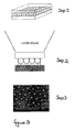
- This application can be understood better with reference to Figure 3 .
- the micro-optical assembly is placed directly onto the product or material that needs to be marked (step 1). It is then exposed to UV laser light (step 2).
- the microspheres which are the main components of the micro optical assembly, act as microlenses, and refract the UV light onto the surface of the material to produce the 2-D pattern (step 3). Accordingly, it results in a permanent imprint of a specific mark, which can not be altered without showing evidence of tampering.
- the provision of a laser data code formed by this technique allow manufacturers and retailers to remove from their inventories any products which are found to lack the necessary identification codes, which could occur for example if their produce were to be copied.
- the micro-optical assembly can therefore be used for marking for example in treasury, pharmaceutical, medical devices and microelectronics fields.
- the use of the optical assembly of the present invention in contact with or very close to the surface as described above has the advantage that individual marks will be easier to identify and read.
- the imprint produced by this technique could be a patterned modification of the colour or monochromatic tone of a region of the surface, a patterned discolouration of the surface, or a patterned physical modification of the surface.
- the imprint could be a modification of the surface texture, such that the light scattering from the modified region is itself modified, or a patterned modification of the surface texture, such that the pattern produced diffracts light in a characteristic manner.
- This technique could be used for example to form a diffractive optic element which, under suitable visible or invisible illumination, reconstructs a computer-generated hologram pattern. Alternatively, it could reconstruct a plurality of surface pits in a pattern, or a plurality of perforations of a surface layer, coating, film or membrane, or a plurality of holes in a material or workpiece. It will be appreciated that in some applications of the invention, more than one type of mark could be formed by the pattern of the micro-optical assembly.
- the modification of the material by the micro-optical assembly being exposed to the laser light may be visible, or invisible under optical spectrum illumination, or may be too small in total area or too fine in pattern resolution to be observable with the unaided human eye.
- the modification may also require advanced optical measurement techniques, including but not limited to electron microscopy, diffraction pattern measurements and colour-specific illumination and/or detection, microscopy, photon-counting, machine-vision or invisible illumination to be observed or detected, or for the information encoded on the material to be detected or decoded or otherwise read out.
- micro-optical assembly of the present invention can also be used in laser shot peening, if the laser has sufficient intensity.
- the micro-optical assembly of the present invention can also be used to produce perforations in a thin membrane for drug delivery or osmostic devices. This has been applied to a biocapsule, for example. This can then be used for effective immunoisolation of transplanted islet cells for treatment of diabetes. These membranes are designed to allow the permeability of glucose, insulin and other metabolically active products, while at the same time, preventing the passage of cytotoxic cells, macrophages, antibodies and complement.
- the formation of a plurality of perforations in a membrane by using the micro-optical assembly of this invention may be controlled by means of a suitable choice of the laser intensity and wavelength to which the micro-optical assembly is to be exposed, and by a suitable choice of the separation between the micro-optical assembly and the membrane, in order that the perforation mean size and standard deviation is such as to facilitate osmosis of one or more substances or species across the membrane, or to facilitate drug elution from a container, pill, capsule or structure.
- the formation of a plurality of holes in a material of structure using the micro-optical assembly of the invention may also be applied to the formation of a hole pattern in a device used for fluid transfer, such as a catheter, canula, or hypodermic needle.
- a Shack-Hartmann wavefront sensor comprising a plurality of micro-lenses in an ordered assembly formed, by the process of the present invention, can be used in order to perform measurements of the distortion of an optical wavefront. Furthermore, it may be used as part of a larger adaptive optics system, for the purpose of performing corrections to the wavefront, based upon the information gathered using the said Shack-Hartmann wavefront sensor.
- the microlens technology of the present invention in conjunction with self-aligned integrated microfluidic optical systems can also be used for fluorescent analysis.
- the planar microlenses have the optical axis parallel to the plane.
- the excitation light of an LED for example is therefore condensed through the planar microspheres, and focused to the detection point in the microfluidic channel.
- the emitted fluorescence may be collected by a detector, which is on the microfluidic channel. Therefore, the whole optical path between excitation and detection consist of mutually orthogonal paths.
- the resulting fluorescent intensity is significantly amplified by the addition of these planar microlenses. It also offers the advantage of being cost-effective, rapid, of having increased fluorescence amplification and also minimises optical aberrations when compared to prior art techniques.
- the microlens technology of the present invention can also be used in multiplexor/demultiplexor optical communications.
- wavelength multiplexing and demultiplexing technologies enable transmission of an increased volume of information in the same optical fibre.
- the relative bandwidth ratio is enhanced, and the light beams are directed directly to the diffraction grating.
- each of the microlenses has to be offset relative to the core of the associated fibre. The amplitude of this offset depends on the position of the fibre, and it is possible using a microlens assembly having a pitch smaller than the pitch of the fibre ends.
Landscapes
- Engineering & Computer Science (AREA)
- Manufacturing & Machinery (AREA)
- Physics & Mathematics (AREA)
- Health & Medical Sciences (AREA)
- Ophthalmology & Optometry (AREA)
- Mechanical Engineering (AREA)
- General Physics & Mathematics (AREA)
- Optics & Photonics (AREA)
- Micromachines (AREA)
Abstract
The present invention relates to a method of manufacturing a micro-optical assembly. The method comprising the steps of: depositing silica microspheres on a first wettable substrate; coating a second substrate with an adhesive material to form an adhesive layer; combining the first and second substrates such that the spheres are partially coated by the adhesive layer; curing the adhesive layer; and removing the first substrate from the second substrate so that an micro-optical assembly is formed by the second substrate having thereon an adherent assembly of microspheres.
Description
- Microlens or micro-optical technology is widely used in a number of different industrial applications. These include fluorescence analyses, sensors, optical communications, laser surface modification, laser marking and coding applications, laser perforation, and laser drilling.
- Micro-optical assemblies can be manufactured using a number of techniques. Once commonly used fabrication technique for micro-optical assemblies involves machining bulk optical substrates with elements which are greater than 100 micrometres, and which can be any value up to a few millimetres in size.
- Another fabrication technique for micro-optical assemblies is described in
US Patent No. 7,057,832 . This Patent describes a micro-optical array which can be used to form an image on a substrate surface. The micro-optical array is formed by the use of a spherically-shaped polystyrene micro-optical component embedded in a polydimethylsiloxane (PDMS) support element. - One disadvantage of the resulting micro-optical component relates to the fact that when used in laser applications, it is found that the transmission is not optimum below wavelengths of 300 nanometres. In fact, it is found that the polystyrene will not transmit light at a wavelength below 266 nanometres.
- Accordingly, the microlens array is not very suited to some applications, such as laser marking, which often require the use of ultraviolet lasers or lamps at shorter wavelengths than 266 nanometres.
- It is therefore an object of the present invention to develop an alternative micro-optical assembly which can be used in a variety of industrial applications.
- The present invention provides a method of manufacturing a micro-optical assembly comprising the following steps:
- depositing silica microspheres on a first wettable substrate;
- coating a second substrate with an adhesive material to form an adhesive layer; combining the first and second substrates such that the spheres are partially coated by the adhesive layer;
- curing the adhesive layer; and
- removing the first substrate from the second substrate so that an micro-optical assembly is formed by the second substrate having thereon an adherent assembly of microspheres.
- The characteristics of the resulting fabricated micro optical assembly make it suitable for use in a variety of industrial applications, such as laser marking technology, laser shot peening, medical applications, wavefront sensors, SiMOS systems and optical communication systems. These characteristics include the fact that the optical assembly can withstand the intensities used in laser material processing, and need not be disposed of after a single usage.
- Preferably, the step of depositing silica microspheres on a first wettable substrate comprises the following steps:
- providing a first wettable substrate; and
- depositing the silica microspheres in a liquid suspension onto the first substrate by a self-assembly process.
- Where the first substrate is glass, the step of providing a first wettable substrate may comprise:
- coating the glass substrate with functionalising agent;
- allowing the functionalising agent to react with the glass substrate for an extended time period;
and heating the reacted combination of functionalising agent and glass substrate. - Where the first substrate is a surface modified polymer, the step of providing the first wettable substrate may comprise:
- cleaning the polymer substrate in an ultrasonic bath; and
- exposing the surface of the polymer substrate to ultraviolet light.
- The self-assembly process may comprise gravitational sedimentation or vertical deposition.
- The gravitational sedimentation process may comprise:
- depositing the microsphere suspension onto the substrate using a micropipette, and
- slowly evaporating the aqueous suspension in a controlled humidity environment, and the vertical deposition process may comprise:
- placing the substrate vertically in a vial containing the suspension of microspheres so that the meniscus is slowly swept across the substrate by solvent evaporation so as to form a monolayer.
- The step of coating a second substrate with an adhesive material to form an adhesive layer may be provided by spin coating, preferably a 2-stage spin process.
- The step of coating a second substrate with an adhesive material to form an adhesive layer may comprise selective deposition of an adhesive material at locations on the second substrate where it is desired to adhere a microsphere.
- Preferably, the selective deposition is provided by programmable means.
- The adhesive material may comprise Cy-52-276 silicone gel or TEOS.
- The present invention also provides a micro-optical assembly formed by the method.
- The present invention also provides the use of the micro-optical assembly in a laser marking apparatus or a laser shot peening apparatus or a Shack-Hartmann wavefront sensor.
- The present invention also provides an apparatus for producing perforations in a membrane comprising the micro-optical assembly.
- The present invention also provides a self-aligned microfluidic optical system (SiMOS) comprising the micro-optical assembly.
- The present invention also provides an optical communication system comprising the micro-optical assembly.
-
-
Figure 1 shows a graphical illustration of the main steps involved in the fabrication of the micro-optical assembly of the present invention. -
Figure 2 shows a typical process flow for the fabrication of the micro-optical assembly of the present invention; and -
Figure 3 shows the application of the micro-optical assembly in laser processing of materials. - The present invention will now be described with reference to an exemplary embodiment shown in the accompanying drawings.
- Referring now to
Figures 1 and2 , instep 1 of the process flow for fabrication of the micro-optical assembly of the present invention,silica microspheres 100 with an approximate refractive index value nsilica spheres =1.37 are deposited onto awettable substrate 110. Thesubstrate 110 may take the form of a clean glass surface, or of a surface modified polymer, for example, a polyimide substrate such as Kapton™. - The process of depositing the silica microspheres onto the wettable substrate requires a number of preparatory steps. Firstly, the fused silica substrates are cleaned using piranic acid (75% sulphuric acid and 25% hydrogen peroxide), rinsed with distilled water and dried before use. In the described embodiment, these silica microspheres are 0.5 - 10 micrometres in diameter.
- Where a glass substrate is used, the glass substrate must then be coated with allyltrimethoxysilane, in order to functionalise the surface (step 1a). It will be appreciated that the amount of agent required depends on the area that needs to be treated. A single molecule will typically cover a surface area of approximately 0.5nm2. The functionalising agent is left to react with the glass substrate for an extended period, such as overnight. It is then held around 80°C for approximately 1 hour, to promote covalent bonding of the organosilane to the surface.
- When Kapton™ is used as the wettable substrate, the Kapton™ polyimide surface is made wettable by cleaning it with 100 % ethanol in an ultrasonic bath for approximately 15 minutes, and then exposing it to UV light at a wavelength of 172nm (step 1b). This can be carried out by an excimer lamp operating at 21 mW/cm2.
- It will be appreciated that another substrate could be used other than Kapton™ or glass, and the surface of the substrate could be modified by any suitable technique, such as plasma processing, corona treatment, flame treatment, chemical etching or surface grafting, and be rendered wettable by methods similar to those described above or otherwise.
The silica microspheres, contained in an aqueous suspension, are then deposited, onto the wettable substrate, by a self-assembly process. This can be either gravitational sedimentation or vertical deposition. - In preferred embodiments of the gravitational sedimentation process, a film-forming composition comprising at least a film-forming agent and a solvent, and optionally other chemical species selected from enamels, resins, plasticizing agents, polymerisation promoters, gelling agents, and cross-linking agents is first formed. In one example, a commercially available nail varnish (Rimmel) proved to be a practical film-forming agent for this purpose. This composition is used to produce a thin retaining boundary film wall, such as for example of length and
width 1 cm x 1 cm, on the substrate, to contain the microspheres, so as to form a microsphere suspension. This prevents the spreading of the aqueous suspension of spheres during the evaporation process. The volume of silica microsphere suspension required to produce a monolayer of hexagonally close packed microspheres over a 1 cm x 1 cm area can be calculated using well-known formulae, and need not be elaborated in further detail here. The sphere suspension is deposited onto the substrate (110) using a micropipette, and the monolayers of microsphere arrays are then formed by slow evaporation of the diluted aqueous suspension in a controlled humidity environment (120). The suspension of the microspheres in liquid ensures that a good spreading of the microspheres can be achieved. - In the vertical deposition (or dip-coating) process, strong capillary forces at a meniscus between the substrate and the microsphere suspension can induce ordering of the microspheres into a hexagonally closed packed array. This is achieved by placing the wettable substrate vertically in a vial containing a suspension of silica spheres. When the meniscus is slowly swept across a vertically placed substrate by solvent evaporation, a monolayer is formed. Once the fluid is evaporated, these spheres self-assemble into a monolayer (120).
- In step 2a, an adhesive material such as CY-52-276 silicone gel or Tetraethylorthosilicate (TEOS, SiO2 precursor), or another suitable adhesive material, is chosen. The refractive indices of the silicone gel, TEOS or other adhesive are approximately equal to or greater than the refractive index of the silica spheres, being approximately in the range 1.38 - 1.5 (nsilicone gel= 1.4; nTEOS = 1.38). The silicone gel, TEOS or other adhesive material is spin coated so as to form an adhesive layer (125) on a second fused silica substrate (130). This is performed to produce a thin layer of either approximately 5 micrometres of silicone gel or approximately 1.7 micrometres of TEOS. In any case the adhesive layer thickness will be less than the diameter of the silica spheres being used. The spin coating is carried out at specific spin times and speeds.
- The spin coating is performed using a spin coater which uses a 2-stage spin process. The fused silica is placed on the central vacuum holder and approximately 120 µl of TEOS or approximately 200 µl of PDMS is deposited onto the fused silica surface.
- The 2-stage process allows dispensing of the solution at low speeds, and homogenising of the coating at higher speeds. The parameter that is typically used for dispensing of both solutions is a spin speed of 800rpm for 6 seconds. The parameters used for homogenising of silicone gel and TEOS on the fused silica surface are typically a spin speed of 8000 rpm for 60 seconds and a spin speed of 3000 rpm for 30 seconds respectively. In the described embodiment, the spin coater is a Chemat Technology Model KW-4A.
- In another embodiment of the invention, this step may be replaced by the step of selective deposition of the adhesive material at locations of the substrate where it is desired to adhere a microsphere (
step 2b). A programmable means of deposition, such as for example ink-jet deposition, may be used to achieve this. In this embodiment of the invention, the microlens may be deposited in a programmable pattern, which may embody a code. - In
step 3 of the process flow, the substrates (120) and (130) produced fromstep 1 andstep 2 are sandwiched together, such that the spheres (100) and adhesive (125) are in contact (140). Sufficient pressure is placed on top of the upper substrate (120) containing the spheres (100) to ensure that the spheres (100) contact the lower substrate. It should be noted that, because the diameter of the spheres is larger than the thickness of the adhesion layer, the silica microspheres (100) are only partially coated by the adhesion layer material. It will be appreciated that if the spheres (100) were fully coated by the adhesive, the resulting micro-optical assembly formed by the process would not enable the spheres to focus the incoming light, and would instead cause any incident illumination to diverge. This is due to the fact that the spheres would have a refractive index smaller than that of their fully surrounding adhesive medium (nsilica spheres = 1.37; nTEOS = 1.38 and nsilicone gel= 1.4). - The adhesive layer (125) is then cured (step 4). This is achieved by curing the silicone gel or the TEOS in a Memment laboratory oven at 70°C for approximately 30 minutes and at 80°C for 6 hours respectively.
- In step 5 of the process flow, the upper substrate (120) is then removed from contact with the lower substrate (130). This can be performed by any suitable means. In one embodiment of the invention, this is performed by manual means, such as by the use of a tweezers. In another embodiment of the invention, an automated mechanical means may be used to remove the upper substrate. At this point, the remaining substrate (130) comprises the completed fabricated micro optical assembly (150), which consists of the second substrate (130) with an adherent array of microspheres (100) (step 6).
- It will be appreciated that the resulting micro-optical assembly consists of a plurality of microlenses. In some embodiments, this can comprise a selectively deposited assembly of microlenses in a pattern determined by the programmable deposition of the adhesive layer. In other embodiments however, the micro optical assembly can exhibit partial, short range, or long-range ordered packing of the microelenses, so as to form of an array of a plurality of microlenses. This array can comprise for example of a hexagonally close packed configuration. Other embodiments may comprise square packing configuration. The area of the micro-optical assembly is typically 1cm x 1cm.
- The characteristics of the resulting fabricated micro optical assembly make it suitable for use in a variety of industrial applications. These include the fact that the optical assembly can withstand the intensities used in laser material processing, and need not be disposed of after a single usage.
- Another advantage of the design of the optical assembly of the present invention is that the micro spheres are in contact with, or close to, the surface of the workpiece when in use in, for example, laser machining or marking applications, rather than being positioned essentially equal to the image distance of the optical component, as is the case with a number of prior art arrangements. When working at distances less than the image distance of the optical component in laser machining or marking applications a larger fraction of the underlying surface is exposed to laser radiation.
- One application in which the microsphere optical assembly of the present invention is suitable for use is in laser marking technology. In this application, the microsphere optical assembly can be used with a laser of sufficient intensity and suitable wavelength to create an imprint of a 2D pattern to form an authentication code on a product or workpiece material, which is invisible to the naked eye. The pattern can be either an ordered or a random pattern, depending on the user requirements. This application can be understood better with reference to
Figure 3 . As is shown from the figure, the micro-optical assembly is placed directly onto the product or material that needs to be marked (step 1). It is then exposed to UV laser light (step 2). On exposure to the UV light, the microspheres, which are the main components of the micro optical assembly, act as microlenses, and refract the UV light onto the surface of the material to produce the 2-D pattern (step 3). Accordingly, it results in a permanent imprint of a specific mark, which can not be altered without showing evidence of tampering. The provision of a laser data code formed by this technique allow manufacturers and retailers to remove from their inventories any products which are found to lack the necessary identification codes, which could occur for example if their produce were to be copied. The micro-optical assembly can therefore be used for marking for example in treasury, pharmaceutical, medical devices and microelectronics fields. The use of the optical assembly of the present invention in contact with or very close to the surface as described above has the advantage that individual marks will be easier to identify and read. - The imprint produced by this technique could be a patterned modification of the colour or monochromatic tone of a region of the surface, a patterned discolouration of the surface, or a patterned physical modification of the surface. Alternatively, the imprint could be a modification of the surface texture, such that the light scattering from the modified region is itself modified, or a patterned modification of the surface texture, such that the pattern produced diffracts light in a characteristic manner.
- This technique could be used for example to form a diffractive optic element which, under suitable visible or invisible illumination, reconstructs a computer-generated hologram pattern. Alternatively, it could reconstruct a plurality of surface pits in a pattern, or a plurality of perforations of a surface layer, coating, film or membrane, or a plurality of holes in a material or workpiece. It will be appreciated that in some applications of the invention, more than one type of mark could be formed by the pattern of the micro-optical assembly.
- It will be appreciated that the modification of the material by the micro-optical assembly being exposed to the laser light may be visible, or invisible under optical spectrum illumination, or may be too small in total area or too fine in pattern resolution to be observable with the unaided human eye. The modification may also require advanced optical measurement techniques, including but not limited to electron microscopy, diffraction pattern measurements and colour-specific illumination and/or detection, microscopy, photon-counting, machine-vision or invisible illumination to be observed or detected, or for the information encoded on the material to be detected or decoded or otherwise read out.
- The micro-optical assembly of the present invention can also be used in laser shot peening, if the laser has sufficient intensity.
- The micro-optical assembly of the present invention can also be used to produce perforations in a thin membrane for drug delivery or osmostic devices. This has been applied to a biocapsule, for example. This can then be used for effective immunoisolation of transplanted islet cells for treatment of diabetes. These membranes are designed to allow the permeability of glucose, insulin and other metabolically active products, while at the same time, preventing the passage of cytotoxic cells, macrophages, antibodies and complement.
- The formation of a plurality of perforations in a membrane by using the micro-optical assembly of this invention may be controlled by means of a suitable choice of the laser intensity and wavelength to which the micro-optical assembly is to be exposed, and by a suitable choice of the separation between the micro-optical assembly and the membrane, in order that the perforation mean size and standard deviation is such as to facilitate osmosis of one or more substances or species across the membrane, or to facilitate drug elution from a container, pill, capsule or structure.
- The formation of a plurality of holes in a material of structure using the micro-optical assembly of the invention may also be applied to the formation of a hole pattern in a device used for fluid transfer, such as a catheter, canula, or hypodermic needle.
- In another industrial application of the present invention, a Shack-Hartmann wavefront sensor, comprising a plurality of micro-lenses in an ordered assembly formed, by the process of the present invention, can be used in order to perform measurements of the distortion of an optical wavefront. Furthermore, it may be used as part of a larger adaptive optics system, for the purpose of performing corrections to the wavefront, based upon the information gathered using the said Shack-Hartmann wavefront sensor.
- The microlens technology of the present invention in conjunction with self-aligned integrated microfluidic optical systems (SiMOS) can also be used for fluorescent analysis. The planar microlenses have the optical axis parallel to the plane. The excitation light of an LED for example is therefore condensed through the planar microspheres, and focused to the detection point in the microfluidic channel. The emitted fluorescence may be collected by a detector, which is on the microfluidic channel. Therefore, the whole optical path between excitation and detection consist of mutually orthogonal paths. The resulting fluorescent intensity is significantly amplified by the addition of these planar microlenses. It also offers the advantage of being cost-effective, rapid, of having increased fluorescence amplification and also minimises optical aberrations when compared to prior art techniques.
- The microlens technology of the present invention can also be used in multiplexor/demultiplexor optical communications. As is well known, wavelength multiplexing and demultiplexing technologies enable transmission of an increased volume of information in the same optical fibre. By adding a microlens assembly to the end of these fibres, the relative bandwidth ratio is enhanced, and the light beams are directed directly to the diffraction grating. In order to have these beams illuminating a common area on the grating and then to reduce loss, each of the microlenses has to be offset relative to the core of the associated fibre. The amplitude of this offset depends on the position of the fibre, and it is possible using a microlens assembly having a pitch smaller than the pitch of the fibre ends.
- The words "comprises/comprising" and the words "having/including" when used herein with reference to the present invention are used to specify the presence of stated features, integers, steps or components but does not preclude the presence or addition of one or more other features, integers, steps, components or groups thereof.
- It is appreciated that certain features of the invention, which are, for clarity, described in the context of separate embodiments, may also be provided in combination in a single embodiment. Conversely, various features of the invention which are, for brevity, described in the context of a single embodiment, may also be provided separately or in any suitable sub-combination.
Claims (15)
- A method of manufacturing a micro-optical assembly comprising the following steps:depositing silica microspheres on a first wettable substrate;coating a second substrate with an adhesive material to form an adhesive layer; combining the first and second substrates such that the spheres are partially coated by the adhesive layer;curing the adhesive layer; andremoving the first substrate from the second substrate so that an micro-optical assembly is formed by the second substrate having thereon an adherent assembly of microspheres.
- The method of Claim 1 wherein the step of depositing silica microspheres on a first wettable substrate comprises the following steps:providing a first wettable substrate; anddepositing the silica microspheres in a liquid suspension onto the first substrate by a self-assembly process.
- The method of Claim 2, wherein the first substrate is glass, and the step of providing a first wettable substrate comprises:coating the glass substrate with functionalising agent;allowing the functionalising agent to react with the glass substrate for an extended time period;
and heating the reacted combination of functionalising agent and glass substrate. - The method of Claim 2, wherein the first substrate is a surface modified polymer, and the step of providing the first wettable substrate comprises:cleaning the polymer substrate in an ultrasonic bath; andexposing the surface of the polymer substrate to ultraviolet light.
- The method of any of Claims 2 to 4, wherein the self-assembly process comprises gravitational sedimentation or vertical deposition.
- The method of Claim 5, wherein the gravitational sedimentation process comprises:depositing the microsphere suspension onto the substrate using a micropipette, andslowly evaporating the aqueous suspension in a controlled humidity environment, and the vertical deposition process comprises:placing the substrate vertically in a vial containing the suspension of microspheres so that the meniscus is slowly swept across the substrate by solvent evaporation so as to form a monolayer.
- The method of any of the previous claims, wherein the step of coating a second substrate with an adhesive material to form an adhesive layer is provided by spin coating, preferably a 2-stage spin process.
- The method of any of the previous claims, wherein the step of coating a second substrate with an adhesive material to form an adhesive layer comprises selective deposition of an adhesive material at locations on the second substrate where it is desired to adhere a microsphere.
- The method of Claim 8, wherein the selective deposition is provided by programmable means.
- The method of any of the previous claims, wherein the adhesive material comprises Cy-52-276 silicone gel or TEOS.
- A micro-optical assembly formed by the method of any of Claims 1 to 10.
- Use of the micro-optical assembly of Claim 11 in a laser marking apparatus or a laser shot peening apparatus or a Shack-Hartmann wavefront sensor.
- An apparatus for producing perforations in a membrane comprising the micro-optical assembly of Claim 11.
- A self-aligned microfluidic optical system (SiMOS) comprising the micro-optical assembly of Claim 11.
- An optical communication system comprising the micro-optical assembly of Claim 11.
Priority Applications (2)
| Application Number | Priority Date | Filing Date | Title |
|---|---|---|---|
| EP08156864A EP2123433A1 (en) | 2008-05-23 | 2008-05-23 | Micro-optical assembly |
| PCT/EP2009/056245 WO2009141436A1 (en) | 2008-05-23 | 2009-05-22 | Micro-optical assembly |
Applications Claiming Priority (1)
| Application Number | Priority Date | Filing Date | Title |
|---|---|---|---|
| EP08156864A EP2123433A1 (en) | 2008-05-23 | 2008-05-23 | Micro-optical assembly |
Publications (1)
| Publication Number | Publication Date |
|---|---|
| EP2123433A1 true EP2123433A1 (en) | 2009-11-25 |
Family
ID=39870501
Family Applications (1)
| Application Number | Title | Priority Date | Filing Date |
|---|---|---|---|
| EP08156864A Withdrawn EP2123433A1 (en) | 2008-05-23 | 2008-05-23 | Micro-optical assembly |
Country Status (2)
| Country | Link |
|---|---|
| EP (1) | EP2123433A1 (en) |
| WO (1) | WO2009141436A1 (en) |
Cited By (3)
| Publication number | Priority date | Publication date | Assignee | Title |
|---|---|---|---|---|
| WO2015025174A1 (en) * | 2013-08-22 | 2015-02-26 | Bangor University | Improvements in and relating to lenses |
| WO2015113105A1 (en) * | 2014-01-31 | 2015-08-06 | The Australian National University | Fabricating lenses using gravity |
| WO2016019131A1 (en) * | 2014-07-31 | 2016-02-04 | University Of Houston System | Fabrication of lenses by droplet formation on a pre-heated surface |
Families Citing this family (2)
| Publication number | Priority date | Publication date | Assignee | Title |
|---|---|---|---|---|
| US9726874B2 (en) | 2012-06-07 | 2017-08-08 | The University Of North Carolina At Charlotte | Methods and systems for super-resolution optical imaging using high-index of refraction microspheres and microcylinders |
| US20180229262A1 (en) * | 2015-07-28 | 2018-08-16 | Agency For Science, Technology And Research | Method for self-assembly of nanoparticles on substrate |
Citations (1)
| Publication number | Priority date | Publication date | Assignee | Title |
|---|---|---|---|---|
| US20040027675A1 (en) * | 2001-04-10 | 2004-02-12 | Ming-Hsien Wu | Microlens for projection lithography and method of preparation thereof |
-
2008
- 2008-05-23 EP EP08156864A patent/EP2123433A1/en not_active Withdrawn
-
2009
- 2009-05-22 WO PCT/EP2009/056245 patent/WO2009141436A1/en not_active Ceased
Patent Citations (2)
| Publication number | Priority date | Publication date | Assignee | Title |
|---|---|---|---|---|
| US20040027675A1 (en) * | 2001-04-10 | 2004-02-12 | Ming-Hsien Wu | Microlens for projection lithography and method of preparation thereof |
| US7057832B2 (en) | 2001-04-10 | 2006-06-06 | President And Fellows Of Harvard College | Microlens for projection lithography and method of preparation thereof |
Non-Patent Citations (2)
| Title |
|---|
| MING-HSIEN WU ET AL: "Patterning flood illumination with microlens arrays", APPLIED OPTICS OPT. SOC. AMERICA USA, vol. 41, no. 13, 1 May 2002 (2002-05-01), pages 2575 - 2585, XP002501846, ISSN: 0003-6935 * |
| SUN Z ET AL: "Fabricating colloidal crystals and construction of ordered nanostructures", NANOSCALE RESEARCH LETTERS JUNE 2006 SPRINGER NEW YORK LLC US, vol. 1, no. 1, June 2006 (2006-06-01), pages 46 - 56, XP002501845 * |
Cited By (6)
| Publication number | Priority date | Publication date | Assignee | Title |
|---|---|---|---|---|
| WO2015025174A1 (en) * | 2013-08-22 | 2015-02-26 | Bangor University | Improvements in and relating to lenses |
| GB2537217A (en) * | 2013-08-22 | 2016-10-12 | Bangor Univ | Improvements in and relating to lenses |
| WO2015113105A1 (en) * | 2014-01-31 | 2015-08-06 | The Australian National University | Fabricating lenses using gravity |
| CN106233191A (en) * | 2014-01-31 | 2016-12-14 | 澳大利亚国立大学 | Gravity is used to manufacture lens |
| WO2016019131A1 (en) * | 2014-07-31 | 2016-02-04 | University Of Houston System | Fabrication of lenses by droplet formation on a pre-heated surface |
| US9995851B2 (en) | 2014-07-31 | 2018-06-12 | University Of Houston System | Fabrication of lenses by droplet formation on a pre-heated surface |
Also Published As
| Publication number | Publication date |
|---|---|
| WO2009141436A1 (en) | 2009-11-26 |
Similar Documents
| Publication | Publication Date | Title |
|---|---|---|
| Jiang et al. | Selective deposition in layer-by-layer assembly: Functional graft copolymers as molecular templates | |
| US9802374B2 (en) | Biopolymer sensor and method of manufacturing the same | |
| EP2086749B1 (en) | Nanopatterned biopolymer optical device and method of manufacturing the same | |
| Bai et al. | Bio-inspired vapor-responsive colloidal photonic crystal patterns by inkjet printing | |
| Galeotti et al. | Self-assembly on optical fibers: a powerful nanofabrication tool for next generation “lab-on-fiber” optrodes | |
| Zhai et al. | pH-gated porosity transitions of polyelectrolyte multilayers in confined geometries and their application as tunable Bragg reflectors | |
| US20040216835A1 (en) | Method for making a multiwell plate having transparent well bottoms | |
| WO2009141436A1 (en) | Micro-optical assembly | |
| Liu et al. | Simple and low‐cost plasmonic fiber‐optic probe as SERS and biosensing platform | |
| WO2008009803A2 (en) | Production of microfluidic polymeric devices by photo-assisted and/ or thermally assisted printing | |
| WO2008118211A2 (en) | Biopolymer photonic crystals and method of manufacturing the same | |
| EP3811078B1 (en) | A method and device for assaying the interaction and dynamics of permeation of a molecule and a lipid bilayer | |
| Barber et al. | Mesoscale block copolymers | |
| CN102612482A (en) | Micro-channel structure method and apparatus | |
| US7616844B2 (en) | Fabrication of fiber optic probes | |
| Pfohl et al. | Controlled modification of microstructured silicon surfaces for confinement of biological macromolecules and liquid crystals | |
| KR20200079494A (en) | Polymer film-metal composite | |
| KR102421564B1 (en) | Printing an adhesive pattern on an anti-fouling support | |
| CN113117765A (en) | Detection chip for photonic crystal coding, preparation method and application thereof, and drug screening system and drug screening method | |
| US10274504B2 (en) | Encoded microcapsules and microarray fabricated therefrom | |
| KR100965632B1 (en) | Micro or nanofluidic chip consisting of NOA channel including thin film PDMS layer and method for manufacturing same | |
| RU2814420C2 (en) | Fabrication of flow cell with planar waveguide | |
| Iwasaki et al. | Photochemical formation of hollow silicone microcapsule arrays on periodic microswelling structures of silicone rubber using 193 nm ArF excimer laser for microencapsulation of electrolytes | |
| WO2017151901A1 (en) | Medical surfaces indicating sterilization or disinfection, and methods of making and using the same | |
| Kartsev et al. | Omniphobic Photoresist‐Assisted Patterning of Porous Polymethacrylate Films |
Legal Events
| Date | Code | Title | Description |
|---|---|---|---|
| PUAI | Public reference made under article 153(3) epc to a published international application that has entered the european phase |
Free format text: ORIGINAL CODE: 0009012 |
|
| AK | Designated contracting states |
Kind code of ref document: A1 Designated state(s): AT BE BG CH CY CZ DE DK EE ES FI FR GB GR HR HU IE IS IT LI LT LU LV MC MT NL NO PL PT RO SE SI SK TR |
|
| AX | Request for extension of the european patent |
Extension state: AL BA MK RS |
|
| AKX | Designation fees paid | ||
| REG | Reference to a national code |
Ref country code: DE Ref legal event code: 8566 |
|
| STAA | Information on the status of an ep patent application or granted ep patent |
Free format text: STATUS: THE APPLICATION IS DEEMED TO BE WITHDRAWN |
|
| 18D | Application deemed to be withdrawn |
Effective date: 20100526 |