EP2122763B1 - Planar tripolar antenna - Google Patents
Planar tripolar antenna Download PDFInfo
- Publication number
- EP2122763B1 EP2122763B1 EP08700180A EP08700180A EP2122763B1 EP 2122763 B1 EP2122763 B1 EP 2122763B1 EP 08700180 A EP08700180 A EP 08700180A EP 08700180 A EP08700180 A EP 08700180A EP 2122763 B1 EP2122763 B1 EP 2122763B1
- Authority
- EP
- European Patent Office
- Prior art keywords
- elements
- antenna
- antenna according
- substrate
- dielectric material
- Prior art date
- Legal status (The legal status is an assumption and is not a legal conclusion. Google has not performed a legal analysis and makes no representation as to the accuracy of the status listed.)
- Not-in-force
Links
- 239000000758 substrate Substances 0.000 claims abstract description 21
- 239000003989 dielectric material Substances 0.000 claims abstract description 17
- 230000008054 signal transmission Effects 0.000 claims abstract description 10
- 230000035945 sensitivity Effects 0.000 claims abstract description 8
- 238000000926 separation method Methods 0.000 claims description 5
- 230000005404 monopole Effects 0.000 claims description 3
- 230000001419 dependent effect Effects 0.000 claims 1
- 230000005684 electric field Effects 0.000 description 11
- 239000004020 conductor Substances 0.000 description 9
- 230000001902 propagating effect Effects 0.000 description 7
- 230000005540 biological transmission Effects 0.000 description 5
- 238000004891 communication Methods 0.000 description 5
- 230000010287 polarization Effects 0.000 description 5
- 230000005670 electromagnetic radiation Effects 0.000 description 3
- 230000001413 cellular effect Effects 0.000 description 2
- 238000004519 manufacturing process Methods 0.000 description 2
- 239000000463 material Substances 0.000 description 2
- 238000000034 method Methods 0.000 description 2
- RYGMFSIKBFXOCR-UHFFFAOYSA-N Copper Chemical compound [Cu] RYGMFSIKBFXOCR-UHFFFAOYSA-N 0.000 description 1
- 230000001154 acute effect Effects 0.000 description 1
- 230000003044 adaptive effect Effects 0.000 description 1
- 238000010276 construction Methods 0.000 description 1
- 229910052802 copper Inorganic materials 0.000 description 1
- 239000010949 copper Substances 0.000 description 1
- 238000006880 cross-coupling reaction Methods 0.000 description 1
- 230000001939 inductive effect Effects 0.000 description 1
- 239000002184 metal Substances 0.000 description 1
- 229910052751 metal Inorganic materials 0.000 description 1
- 239000007769 metal material Substances 0.000 description 1
- 150000002739 metals Chemical class 0.000 description 1
Images


Classifications
-
- H—ELECTRICITY
- H01—ELECTRIC ELEMENTS
- H01Q—ANTENNAS, i.e. RADIO AERIALS
- H01Q21/00—Antenna arrays or systems
- H01Q21/24—Combinations of antenna units polarised in different directions for transmitting or receiving circularly and elliptically polarised waves or waves linearly polarised in any direction
- H01Q21/26—Turnstile or like antennas comprising arrangements of three or more elongated elements disposed radially and symmetrically in a horizontal plane about a common centre
-
- H—ELECTRICITY
- H01—ELECTRIC ELEMENTS
- H01Q—ANTENNAS, i.e. RADIO AERIALS
- H01Q21/00—Antenna arrays or systems
- H01Q21/28—Combinations of substantially independent non-interacting antenna units or systems
-
- H—ELECTRICITY
- H01—ELECTRIC ELEMENTS
- H01Q—ANTENNAS, i.e. RADIO AERIALS
- H01Q9/00—Electrically-short antennas having dimensions not more than twice the operating wavelength and consisting of conductive active radiating elements
- H01Q9/04—Resonant antennas
- H01Q9/0407—Substantially flat resonant element parallel to ground plane, e.g. patch antenna
-
- H—ELECTRICITY
- H01—ELECTRIC ELEMENTS
- H01Q—ANTENNAS, i.e. RADIO AERIALS
- H01Q9/00—Electrically-short antennas having dimensions not more than twice the operating wavelength and consisting of conductive active radiating elements
- H01Q9/04—Resonant antennas
- H01Q9/16—Resonant antennas with feed intermediate between the extremities of the antenna, e.g. centre-fed dipole
- H01Q9/26—Resonant antennas with feed intermediate between the extremities of the antenna, e.g. centre-fed dipole with folded element or elements, the folded parts being spaced apart a small fraction of operating wavelength
- H01Q9/265—Open ring dipoles; Circular dipoles
Definitions
- This invention relates to a planar tripolar antenna, being one which is capable of receiving and/or transmitting electromagnetic radiation which is polarised along three ideally orthogonal, axes.
- dipolar and tripolar antennae at least in terms of providing two or three orthogonally aligned antennae, is known, particularly in the field of wireless data communication, such as is employed in wireless local area network (LAN) cards, Bluetooth®, wireless routers and the like. It has also been considered in the field of mobile cellular telecommunications where the provision of one or more secondary antennae might provide a more reliable, stable, improved and/or effective connection between the base station or signal broadcast mast and the mobile device. For instance, Proc. IEEE, vol. 92, Feb. 2004 (Paulraj et al.) demonstrates that multiple antenna designs are much desired in wireless applications, as they provide significant improvements in signal reliability and data rates.
- Polar antennae arrangements are also known to be spatially more efficient in that they can be effectively miniaturized, and as such prove invaluable for mobile cellular devices where overall product size is of critical importance. (See IEEE Trans. Commun., vol. COM-20, Oct. 1972, Lee & Yeh ).
- a technique known as spatial multiplexing is also known wherein three separate data signals can be transmitted by transmitting/receiving three separate electromagnetic waves, each having one of the three possible linear polarizations of the electric field. It is to be mentioned that the polarisation axes are traditionally, but not necessarily, orthogonal. The ability to communicate three data streams simultaneously in this manner can increase the overall data throughput by a factor of 3 ( Nature, vol. 409, Jan. 2001, Andrews, Mitra, and Carvalho ).
- the two perpendicularly arranged dipoles transmit/receive the two mutually orthogonal polarisations of electric field
- the loop element transmits/receives the magnetic field polarised in the third orthogonal direction, i.e. predominantly about an axis coincident with the geometric centre of the loop.
- the loop element does not provide a useful antenna for the reception or transmission of an electric field polarised in the third orthogonal direction.
- the fundamental inventive realisation behind US6844858 and by which it is concluded that there are potentially six independent polarisation channels, is that for a suitable arrangement of antennae transmitting or receiving electromagnetic waves, there are 3 components of electric field, namely two transverse components, and a longitudinal component.
- the transverse components are capable of propagating from one antenna to another as a result of being disposed in a rich scattering environment, while the longitudinal component propagates directly through space.
- E and H components are typically orthogonal to one another in the far-field - it is these physical factors which led the inventors to deduce that 6 independent channels (3 using E and 3 using H) may exist.
- E and H are only sufficiently decoupled so as to be considered independent in the near-field (for example over the order of a few metres) as opposed to the far-field (for example between mobile telephones and their most proximate transmission/reception antenna, i.e. a few hundred metres or even a few km).
- US 2006/0071870 discloses an antenna device formed by a plurality of linear elements.
- a planar tripolar antenna consisting of a first two electromagnetic signal transmitting/receiving elements which are arranged such that their axes of signal transmission/reception sensitivity are not parallel, characterised in that the antenna also includes a third electromagnetic signal transmitting/receiving element comprised of at least a pair of spaced apart corresponding panels separated by a dielectric material and arranged such that one panel overlays the other, the separation of each corresponding panel being such that the direction of the shortest path between said panels has at least a degree of perpendicularity with the axes of signal transmission/reception sensitivity of the first two elements.
- the direction of the shortest line which can be drawn between the two spaced apart portions of the third electromagnetic signal transmitting/receiving element shall hereinafter be referred to as the axis of separation.
- the axis of separation is substantially perpendicular to both the axes of signal transmission/reception of the first two transmitting/receiving elements, which are themselves preferably substantially perpendicular.
- each of said signal transmitting/receiving elements is provided on or in a substrate of dielectric material.
- portions of said substantially perpendicular two elements are coplanar.
- the two substantially perpendicular elements consist of a pair of dipoles arranged such that one pair of respective ends of said dipoles is proximate and another pair is remote.
- the third element consists of a first panel radiator of circular (or possibly possessing any other two dimensional) cross-sectional shape, a second circular panel radiator (again possibly of different cross-sectional shape).
- Each of said elements may be embedded within the dielectric material substrate or alternatively applied to the upper and/or lower surfaces thereof.
- the panels of the third element are provided on opposite sides of said dielectric material substrate.
- each panel is arranged such that their geometric centres are concentric.
- the arrangement of all the elements of the antenna minimises cross coupling between each element.
- the dipoles may be replaced by horizontally polarised microstrip patch elements.
- the antenna 2 comprises a planar sheet 4 of dielectric forming the substrate of the device in which are provided three independent ports, 6, 8, 10.
- Each port is connected to the feed of one of the antenna elements through a feeder (which may be microstrip, co-planar-waveguide, coaxial cable or other suitable device).
- a feeder which may be microstrip, co-planar-waveguide, coaxial cable or other suitable device.
- the top face contains a laterally oriented dipole 12 (bow tie, or microstrip patch etc.) connected to one port; a transversally oriented dipole 14 connected to a further port; and a circular panel or disk radiator 16 to which one conductor of port 6 is connected.
- On the back face of the dielectric 4 is another disk 18 to which the other (ground) conductor of the port 6 is connected, and which is concentric with the top disk, as shown in Fig. 2(b) .
- a design example of such an element is provided in prior publication Electronics letters, vol.
- the three ports are connected to coaxial cables or other suitable connectors.
- the lengths of the dipoles and the diameters of the disks (along with the dielectric constant of the substrate, e.g., FR4) determine the operating frequency of the antennas.
- the dipoles may be replaced by laterally and transversely polarised microstrip patch elements, which would require a ground plane beneath them. These are well established design elements.
- Fig. 3 shows such a structure in which two generally elongate microstrip patch antenna elements 22, 24 are provided on a high frequency laminate substrate 30 such as an RT/duroidTM substrate.
- the antenna elements 22, 24 are provided with their longitudinal axes generally mutually orthogonal to one another.
- the antenna elements 22, 24 are arranged to be orthogonal to a respective one of a pair of orthogonal edges of the substrate.
- a ground plane 31 in the form of a sheet of conducting material is provided on a side of the substrate opposite the side on which the antenna elements 22, 24 are formed, underlying the region of the substrate over which the elements 22, 24 are formed.
- a conductor of each of the ports 36, 38 of antenna elements 22, 24 is connected to a respective one of each of the antenna elements 22, 24 whilst the other conductor of each port is connected to the ground plane 31.
- the ground plane is a single sheet of a metallic material.
- the conductor is a single sheet of copper.
- Other metals and other conducting materials are also useful.
- Other forms of ground plane are also useful, such as a ground plane comprising multiple patches or strips of material.
- a third antenna element is provided having a circular panel or disk radiator 26 on the same side of the substrate as the antenna elements 22, 24, and a corresponding disk 28 on the reverse side of the substrate in a similar manner to the example of Fig. 2 .
- a conductor of a port 40 of the third antenna is connected to the disk radiator 26 whilst a ground conductor of port 40 is connected to the corresponding disk 28.
- the direction of polarisation of the antenna elements 22, 24 and the third antenna element 26 are indicated in FIG. 3 by arrows A, B, C respectively.
- the patch antenna elements 22, 24 are around 20mm long and 5mm wide, being generally rectangular in shape.
- Some embodiments of the invention having a ground plane provided underlying the antenna elements 22, 24 are found to have reduced sensitivity to the presence of metallic objects in a vicinity of the structure.
- the present invention resides in the fact that none has been combined in this useful and innovative manner before.
- the invention provides a compact antenna design consisting of three independent elements dielectrically isolated from one another and having a planar construction and can transmit and receive all three possible orthogonal polarisations of a propagating electric field, in particular the E field of a propagating electromagnetic wave. It is to be mentioned that the elements do not need to be arranged in exactly orthogonal relationship described above.
- the dipole elements may be arranged at an acute or obtuse angle to one another, and furthermore, the circular disk elements may be embedded partially or fully in the delectric material, and furthermore orientated at a desired elevation relative to the notional z plane, where the x and y axes are in the plane containing the dielectric substrate and the two dipoles.
- the tripolar transmitter/receiver can be configured to act as three independent antennas carrying three separate information streams (signals) or can be configured to operate as a "diversity combining antenna" which can be used to enhance the signal transmission/reception quality of information (bit error rate - BER), or both, optionally in an adaptive configuration.
- Each antenna element is capable of transmitting (or receiving) electromagnetic waves with one of the three possible linear polarisations of the electric field, thereby spanning the full polarisation basis. In this way, an arbitrarily polarised wave can be transmitted or received from any direction.
- the three elements can have individual feeds and can therefore be excited independently. As a result, they can carry independent signals useful for spatial (polarisation) multiplexing.
- the antennas can also be configured to transmit/receive the same information signal through all three polarisations. This allows for the system to be operated as a "diversity" antenna array. There is also the possibility of operating in a combination of both configurations, adapting between the two depending on whether a reliable and robust link is required or a high capacity link is required. It is also possible that two antennas can be operated as a diversity antenna system (both elements carrying the same signal) and the third operating as an independent antenna carrying another information stream.
- planar and compact nature of the antenna can be easily placed on a flat surface, such as the back plate of a mobile phone, a laptop PCMCIA card, or the windshield of a car. It can be directly fabricated as a planar structure, reducing the manufacturing complexity and cost.
- each element may be either wholly encased within the dielectric material, partially inset or recessed, or mounted directly on the surface of the dielectric material. All such configurations are considered within the scope of this invention.
- the transmission/reception characteristics of the antenna may be changed by scaling the dielectric.
- the antenna may be designed to be particularly effective at a particular frequency.
- the first two elements may be monopole elements as opposed to dipoles. Also, instead of supplying electric current to the disk radiators through their edges, they may be centre-fed.
- antenna element designs are possible, such as wideband elements.
- a planar tripolar antenna having at least two electromagnetic signal transmitting/receiving elements arranged such that their axes of signal transmission/reception sensitivity are not parallel, wherein the said elements are provided on or at least partially in a substrate of dielectric material so portions of the said, at least two elements are coplanar and dielectrically isolated from one another.
- two dipoles are provided on the substrate in perpendicular orientation and in the plane containing of the surface of said dielectric material.
- a further third element is provided so as to render the antenna tripolar, said third element comprising a first circular disk element secured to an upper surface of the dielectric material, and a second element, concentrically positioned on the corresponding opposite and lower surface of the dielectric.
Landscapes
- Variable-Direction Aerials And Aerial Arrays (AREA)
- Waveguide Aerials (AREA)
- Details Of Aerials (AREA)
Abstract
Description
- This invention relates to a planar tripolar antenna, being one which is capable of receiving and/or transmitting electromagnetic radiation which is polarised along three ideally orthogonal, axes.
- Document
US 2006/0071870 describing an antenna for wireless LAN system. - The notion of providing dipolar and tripolar antennae, at least in terms of providing two or three orthogonally aligned antennae, is known, particularly in the field of wireless data communication, such as is employed in wireless local area network (LAN) cards, Bluetooth®, wireless routers and the like. It has also been considered in the field of mobile cellular telecommunications where the provision of one or more secondary antennae might provide a more reliable, stable, improved and/or effective connection between the base station or signal broadcast mast and the mobile device. For instance, Proc. IEEE, vol. 92, Feb. 2004 (Paulraj et al.) demonstrates that multiple antenna designs are much desired in wireless applications, as they provide significant improvements in signal reliability and data rates.
- Polar antennae arrangements are also known to be spatially more efficient in that they can be effectively miniaturized, and as such prove invaluable for mobile cellular devices where overall product size is of critical importance. (See IEEE Trans. Commun., vol. COM-20, Oct. 1972, Lee & Yeh).
- A technique known as spatial multiplexing is also known wherein three separate data signals can be transmitted by transmitting/receiving three separate electromagnetic waves, each having one of the three possible linear polarizations of the electric field. It is to be mentioned that the polarisation axes are traditionally, but not necessarily, orthogonal. The ability to communicate three data streams simultaneously in this manner can increase the overall data throughput by a factor of 3 (Nature, vol. 409, Jan. 2001, Andrews, Mitra, and Carvalho).
-
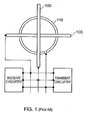
US6844858 to Andrews, Mitra, and Gans further discloses that in a rich scattering environment, there are potentially six, and not merely two or three, independent polarization channels available for the transmission of data. However, this allegation is considered contentious because for free space propagating wave, the magnetic field component is a relativistic manifestation of the electric field component. Therefore there are only 3 available channels, ignoring inductive non-propagating effects. Notwithstanding this, the document discloses a simplified version of a tri-polar antenna which might be considered for use in the invention described. This is shown inFigure 1 hereof, and the twodipole elements loop element 110 which are said to provide the threefold polarization diversity, and the orthogonal arrangement of two ofdipole elements Figure 1 the two perpendicularly arranged dipoles transmit/receive the two mutually orthogonal polarisations of electric field, whereas the loop element transmits/receives the magnetic field polarised in the third orthogonal direction, i.e. predominantly about an axis coincident with the geometric centre of the loop. - One disadvantage of the antenna shown in
Figure 1 is that each of the three antenna are superposed. In the patent, the arrangement of the various elements is described as being substantially in a plane, but actually planar configuration is impossible due to superposition of each of the elements. In applications where space is at a premium, such arrangements may be precluded. - A more pervasive disadvantage of this arrangement is that the loop element does not provide a useful antenna for the reception or transmission of an electric field polarised in the third orthogonal direction. Indeed, the fundamental inventive realisation behind
US6844858 , and by which it is concluded that there are potentially six independent polarisation channels, is that for a suitable arrangement of antennae transmitting or receiving electromagnetic waves, there are 3 components of electric field, namely two transverse components, and a longitudinal component. The transverse components are capable of propagating from one antenna to another as a result of being disposed in a rich scattering environment, while the longitudinal component propagates directly through space. - As is known by those skilled in the art, electromagnetic waves are generally polarised in directions orthogonal to the propagation direction, and thus E and H components (from Maxwell's equations governing electromagnetic theory, E being the electric field vector and H being the magnetic field vector) are typically orthogonal to one another in the far-field - it is these physical factors which led the inventors to deduce that 6 independent channels (3 using E and 3 using H) may exist. However, it is known that E and H are only sufficiently decoupled so as to be considered independent in the near-field (for example over the order of a few metres) as opposed to the far-field (for example between mobile telephones and their most proximate transmission/reception antenna, i.e. a few hundred metres or even a few km).
-
US 2006/0071870 discloses an antenna device formed by a plurality of linear elements. - It is an object of the invention therefore to provide an antenna with multiple polarizations that is of generally planar configuration which is compatible with printed circuit board production techniques.
- It is a further object of this invention to provide an antenna capable of transmitting/receiving electromagnetic radiation having three different electric field polarisations.
- According to the present invention there is provided a planar tripolar antenna consisting of a first two electromagnetic signal transmitting/receiving elements which are arranged such that their axes of signal transmission/reception sensitivity are not parallel, characterised in that the antenna also includes a third electromagnetic signal transmitting/receiving element comprised of at least a pair of spaced apart corresponding panels separated by a dielectric material and arranged such that one panel overlays the other, the separation of each corresponding panel being such that the direction of the shortest path between said panels has at least a degree of perpendicularity with the axes of signal transmission/reception sensitivity of the first two elements.
- For the avoidance of doubt, the direction of the shortest line which can be drawn between the two spaced apart portions of the third electromagnetic signal transmitting/receiving element shall hereinafter be referred to as the axis of separation.
- Preferably, the axis of separation is substantially perpendicular to both the axes of signal transmission/reception of the first two transmitting/receiving elements, which are themselves preferably substantially perpendicular.
- Preferably, each of said signal transmitting/receiving elements is provided on or in a substrate of dielectric material.
- Further preferably, portions of said substantially perpendicular two elements are coplanar.
- Preferably the two substantially perpendicular elements consist of a pair of dipoles arranged such that one pair of respective ends of said dipoles is proximate and another pair is remote.
- Preferably, the third element consists of a first panel radiator of circular (or possibly possessing any other two dimensional) cross-sectional shape, a second circular panel radiator (again possibly of different cross-sectional shape).
- Each of said elements may be embedded within the dielectric material substrate or alternatively applied to the upper and/or lower surfaces thereof.
- In a preferred embodiment, the panels of the third element are provided on opposite sides of said dielectric material substrate.
- Most preferably, each panel is arranged such that their geometric centres are concentric.
- Ideally, the arrangement of all the elements of the antenna minimises cross coupling between each element.
- In an alternative arrangement, the dipoles may be replaced by horizontally polarised microstrip patch elements.
-
-
Figure 1 shows a prior art arrangement of elements constituting a tripolar antenna adapted for the transmission reception of two separate polarisations of a propagating electric field and a third, mutually orthogonal polarisation of a propagating magnetic field; -
Figure 2a, b provide plan views of the upper and lower surface of an antenna according to one embodiment of the invention showing the arrangement of elements; -
Figure 3 shows a perspective view of an antenna according to an embodiment of the invention; and -
Figure 4 shows a perspective view of a possible further embodiment of an antenna according to the invention. - Referring to
Figures 2a, b , which shows merely one possible embodiment of the invention, theantenna 2 comprises aplanar sheet 4 of dielectric forming the substrate of the device in which are provided three independent ports, 6, 8, 10. - Each port is connected to the feed of one of the antenna elements through a feeder (which may be microstrip, co-planar-waveguide, coaxial cable or other suitable device). According to the illustration in the
Fig. 2(a) , the top face contains a laterally oriented dipole 12 (bow tie, or microstrip patch etc.) connected to one port; a transversallyoriented dipole 14 connected to a further port; and a circular panel ordisk radiator 16 to which one conductor ofport 6 is connected. On the back face of the dielectric 4 is anotherdisk 18 to which the other (ground) conductor of theport 6 is connected, and which is concentric with the top disk, as shown inFig. 2(b) . A design example of such an element is provided in prior publication Electronics letters, vol. 33, pp.727-9, 1997 "Patch antenna equivalent to simple monopole" by Economou & Langley. The three ports are connected to coaxial cables or other suitable connectors. The lengths of the dipoles and the diameters of the disks (along with the dielectric constant of the substrate, e.g., FR4) determine the operating frequency of the antennas. The dipoles may be replaced by laterally and transversely polarised microstrip patch elements, which would require a ground plane beneath them. These are well established design elements. -
Fig. 3 shows such a structure in which two generally elongate microstrippatch antenna elements frequency laminate substrate 30 such as an RT/duroid™ substrate. Theantenna elements Fig. 3 theantenna elements - A
ground plane 31 in the form of a sheet of conducting material is provided on a side of the substrate opposite the side on which theantenna elements elements ports antenna elements antenna elements ground plane 31. In the embodiment ofFig. 3 the ground plane is a single sheet of a metallic material. In some embodiments the conductor is a single sheet of copper. Other metals and other conducting materials are also useful. Other forms of ground plane are also useful, such as a ground plane comprising multiple patches or strips of material. - A third antenna element is provided having a circular panel or
disk radiator 26 on the same side of the substrate as theantenna elements corresponding disk 28 on the reverse side of the substrate in a similar manner to the example ofFig. 2 . A conductor of aport 40 of the third antenna is connected to thedisk radiator 26 whilst a ground conductor ofport 40 is connected to thecorresponding disk 28. - The direction of polarisation of the
antenna elements third antenna element 26 are indicated inFIG. 3 by arrows A, B, C respectively. - In one embodiment of the invention, configured to operate at a frequency of 2.4GHz, the
patch antenna elements - Some embodiments of the invention having a ground plane provided underlying the
antenna elements - As will be appreciated, while many of the elements contained in the invention are independently known, the present invention resides in the fact that none has been combined in this useful and innovative manner before. In this regard, the invention provides a compact antenna design consisting of three independent elements dielectrically isolated from one another and having a planar construction and can transmit and receive all three possible orthogonal polarisations of a propagating electric field, in particular the E field of a propagating electromagnetic wave. It is to be mentioned that the elements do not need to be arranged in exactly orthogonal relationship described above. For instance, the dipole elements may be arranged at an acute or obtuse angle to one another, and furthermore, the circular disk elements may be embedded partially or fully in the delectric material, and furthermore orientated at a desired elevation relative to the notional z plane, where the x and y axes are in the plane containing the dielectric substrate and the two dipoles.
- The tripolar transmitter/receiver can be configured to act as three independent antennas carrying three separate information streams (signals) or can be configured to operate as a "diversity combining antenna" which can be used to enhance the signal transmission/reception quality of information (bit error rate - BER), or both, optionally in an adaptive configuration.
- Each antenna element is capable of transmitting (or receiving) electromagnetic waves with one of the three possible linear polarisations of the electric field, thereby spanning the full polarisation basis. In this way, an arbitrarily polarised wave can be transmitted or received from any direction. The three elements can have individual feeds and can therefore be excited independently. As a result, they can carry independent signals useful for spatial (polarisation) multiplexing. The antennas can also be configured to transmit/receive the same information signal through all three polarisations. This allows for the system to be operated as a "diversity" antenna array. There is also the possibility of operating in a combination of both configurations, adapting between the two depending on whether a reliable and robust link is required or a high capacity link is required. It is also possible that two antennas can be operated as a diversity antenna system (both elements carrying the same signal) and the third operating as an independent antenna carrying another information stream.
- As a result of the planar and compact nature of the antenna, such can be easily placed on a flat surface, such as the back plate of a mobile phone, a laptop PCMCIA card, or the windshield of a car. It can be directly fabricated as a planar structure, reducing the manufacturing complexity and cost.
- Referring finally to
Figure 4 , a further embodiment of the invention is shown wherein the dipole elements are both embedded or encased in the dielectric material, and the circular disk elements are provided on the upper and lower surfaces thereof. There are different variations of this configuration which are possible, andFigure 4 shows only one possible configuration. For example, to a greater or lesser extent, each element may be either wholly encased within the dielectric material, partially inset or recessed, or mounted directly on the surface of the dielectric material. All such configurations are considered within the scope of this invention. - It is also to be mentioned that the transmission/reception characteristics of the antenna may be changed by scaling the dielectric. In particular, by suitable selection of dielectric material, thickness, and shape, the antenna may be designed to be particularly effective at a particular frequency. Also, the first two elements may be monopole elements as opposed to dipoles. Also, instead of supplying electric current to the disk radiators through their edges, they may be centre-fed.
- Other antenna element designs are possible, such as wideband elements.
- In terms of backwards compatibility with existing mobile telecommunications networks (to which this invention is ideally suited), such communications are currently achieved using a single dominant polarisation of electromagnetic radiation. Hence with this arrangement, not only can the potential bandwidth be tripled, but backwards compatibility with existing networks can be maintained in new devices embodying the new antenna and means of signal communication.
- Possible uses for each of the three channels made available by this invention are:
- providing different frequencies for communication;
- providing different data streams over the 3 channels at the same frequency;
- providing uplink, downlink etc. on separate channels.
- In summary therefore, a planar tripolar antenna is described having at least two electromagnetic signal transmitting/receiving elements arranged such that their axes of signal transmission/reception sensitivity are not parallel, wherein the said elements are provided on or at least partially in a substrate of dielectric material so portions of the said, at least two elements are coplanar and dielectrically isolated from one another. In a preferred arrangement, two dipoles are provided on the substrate in perpendicular orientation and in the plane containing of the surface of said dielectric material. A further third element is provided so as to render the antenna tripolar, said third element comprising a first circular disk element secured to an upper surface of the dielectric material, and a second element, concentrically positioned on the corresponding opposite and lower surface of the dielectric.
Claims (14)
- A planar tripolar antenna consisting of:a first two electromagnetic signal transmitting/receiving elements (12, 14, 22, 24) which are arranged such that their axes of signal transmission/reception sensitivity are not parallel;characterised in that the antenna also includes a third electromagnetic signal transmitting/receiving element comprised of at least a pair of spaced apart corresponding panels (16, 18, 26, 28) separated by a dielectric material and arranged such that one panel overlays the other, the separation of each corresponding panel (16, 18, 26, 28) being such that the direction of the shortest path between said panels has at least a degree of perpendicularity with the axes of signal transmission/reception sensitivity of the first two elements (12, 14, 22, 24).
- An antenna according to claim 1 wherein the direction of the shortest path between the panels of the third element (16, 18, 26, 28) defines an axis of separation which is substantially perpendicular to both the axes of signal transmission/reception of the first two transmitting/receiving elements (12, 14, 22, 24).
- An antenna according to any preceding claim wherein the axes of signal transmission/reception sensitivity of the first two elements (12, 14, 22, 24) are themselves preferably substantially perpendicular.
- An antenna according to any preceding claim wherein portions of first two elements (12, 14, 22, 24) are coplanar.
- An antenna according to any preceding claim wherein each of the signal transmitting/receiving elements (12, 14, 16, 18, 22, 24, 26, 28) is provided on or in a substrate of dielectric material.
- An antenna according to any preceding claim wherein the first two elements (12, 14, 22, 24) consist of a pair of dipoles arranged such that one pair of respective ends of said dipoles is proximate and another pair is remote.
- An antenna according to any preceding claim wherein the third element (16, 18, 26, 28) consists of first and second circular panel radiators arranged in substantially superposed relationship.
- An antenna according to claim 5 or any claim dependent thereon wherein said elements (12, 14, 16, 18, 22, 24, 26, 28) are surface mounted on the dielectric substrate.
- An antenna according to claim 8 wherein the panels of the third element (16, 18, 26, 28) are provided on opposite sides of said dielectric material substrate.
- An antenna according to claim 8 or claim 9 wherein a ground plane is provided on an opposite side of the substrate to said first two elements (12, 14, 22, 24), the first two elements (12, 14, 22, 24) at least partially overlying said ground plane.
- An antenna as claimed in claim 10 wherein substantially an entire area of each of said first two elements (12, 14, 22, 24) overlies said ground plane.
- An antenna as claimed in claim 10 or claim 11 wherein said ground plane does not underlie panels of the third element (16, 18, 26, 28).
- An antenna according to any preceding claim wherein the first two elements (12, 14, 22, 24) are perpendicularly arranged monopoles or dipoles.
- An antenna according to any of claims 1 to 12 wherein the elements are horizontally polarised microstrip patch elements.
Applications Claiming Priority (2)
| Application Number | Priority Date | Filing Date | Title |
|---|---|---|---|
| GBGB0700218.1A GB0700218D0 (en) | 2007-01-06 | 2007-01-06 | Planar tripolar antenna |
| PCT/GB2008/050004 WO2008081200A1 (en) | 2007-01-06 | 2008-01-02 | Planar tripolar antenna |
Publications (2)
| Publication Number | Publication Date |
|---|---|
| EP2122763A1 EP2122763A1 (en) | 2009-11-25 |
| EP2122763B1 true EP2122763B1 (en) | 2012-03-14 |
Family
ID=37801795
Family Applications (1)
| Application Number | Title | Priority Date | Filing Date |
|---|---|---|---|
| EP08700180A Not-in-force EP2122763B1 (en) | 2007-01-06 | 2008-01-02 | Planar tripolar antenna |
Country Status (5)
| Country | Link |
|---|---|
| US (1) | US8179325B2 (en) |
| EP (1) | EP2122763B1 (en) |
| AT (1) | ATE549768T1 (en) |
| GB (1) | GB0700218D0 (en) |
| WO (1) | WO2008081200A1 (en) |
Families Citing this family (11)
| Publication number | Priority date | Publication date | Assignee | Title |
|---|---|---|---|---|
| EP2210126A4 (en) | 2007-10-24 | 2011-08-31 | Kirsen Technologies Corp | A system and method for space control and remote monitoring |
| US8570229B2 (en) * | 2009-01-15 | 2013-10-29 | Broadcom Corporation | Multiple antenna high isolation apparatus and application thereof |
| US9083086B2 (en) * | 2012-09-12 | 2015-07-14 | City University Of Hong Kong | High gain and wideband complementary antenna |
| CN103858277B (en) * | 2013-12-20 | 2015-12-30 | 华为技术有限公司 | A kind of three poliarizing antennas |
| KR101920748B1 (en) * | 2014-10-20 | 2018-11-21 | 가부시키가이샤 무라타 세이사쿠쇼 | Wireless communication module |
| WO2016063758A1 (en) * | 2014-10-20 | 2016-04-28 | 株式会社村田製作所 | Antenna module |
| CN107112639B (en) * | 2014-12-12 | 2020-10-23 | 华为技术有限公司 | Six-port and six-polarization antenna |
| RU170222U1 (en) * | 2016-12-26 | 2017-04-18 | Акционерное общество "Воронежский научно-исследовательский институт "Вега" (АО "ВНИИ "Вега") | ANTENNA |
| US10897091B2 (en) | 2018-01-12 | 2021-01-19 | University Of South Florida | 3D tripolar antenna and method of manufacture |
| GB202012315D0 (en) | 2020-08-07 | 2020-09-23 | Spectroma Ltd | Microwave imaging system |
| WO2026069938A1 (en) * | 2024-09-24 | 2026-04-02 | 株式会社村田製作所 | Antenna module and communication device |
Family Cites Families (8)
| Publication number | Priority date | Publication date | Assignee | Title |
|---|---|---|---|---|
| US5068669A (en) * | 1988-09-01 | 1991-11-26 | Apti, Inc. | Power beaming system |
| US6400332B1 (en) * | 2001-01-03 | 2002-06-04 | Hon Hai Precision Ind. Co., Ltd. | PCB dipole antenna |
| JP2004266333A (en) | 2003-01-30 | 2004-09-24 | Matsushita Electric Ind Co Ltd | Antenna device |
| US7532114B2 (en) * | 2003-02-03 | 2009-05-12 | Ingrid, Inc. | Fixed part-portable part communications network for a security network |
| CN1734836B (en) * | 2004-08-10 | 2010-11-17 | 富士康(昆山)电脑接插件有限公司 | Antenna |
| KR100597581B1 (en) | 2004-11-05 | 2006-07-06 | 한국전자통신연구원 | Symmetrical Multiband Internal Antenna with Stubs |
| US7408519B2 (en) * | 2005-12-16 | 2008-08-05 | Harris Corporation | Dual polarization antenna array with inter-element capacitive coupling plate and associated methods |
| US7307590B1 (en) * | 2006-05-19 | 2007-12-11 | The United States Of America As Represented By The Secretary Of The Navy | Wideband traveling wave microstrip antenna |
-
2007
- 2007-01-06 GB GBGB0700218.1A patent/GB0700218D0/en not_active Ceased
-
2008
- 2008-01-02 WO PCT/GB2008/050004 patent/WO2008081200A1/en not_active Ceased
- 2008-01-02 US US12/521,595 patent/US8179325B2/en not_active Expired - Fee Related
- 2008-01-02 EP EP08700180A patent/EP2122763B1/en not_active Not-in-force
- 2008-01-02 AT AT08700180T patent/ATE549768T1/en active
Also Published As
| Publication number | Publication date |
|---|---|
| US8179325B2 (en) | 2012-05-15 |
| ATE549768T1 (en) | 2012-03-15 |
| EP2122763A1 (en) | 2009-11-25 |
| WO2008081200A1 (en) | 2008-07-10 |
| GB0700218D0 (en) | 2007-02-14 |
| US20110006960A1 (en) | 2011-01-13 |
Similar Documents
| Publication | Publication Date | Title |
|---|---|---|
| US8179325B2 (en) | Planar tripolar antenna | |
| CN110137675B (en) | Antenna unit and terminal equipment | |
| US10312589B2 (en) | Antenna directivity control system and radio device | |
| US7999749B2 (en) | Antenna assembly | |
| US8085202B2 (en) | Wideband, high isolation two port antenna array for multiple input, multiple output handheld devices | |
| EP3465823B1 (en) | C-fed antenna formed on multi-layer printed circuit board edge | |
| EP2617098B1 (en) | Antenna for diversity operation | |
| KR20170001560U (en) | Wireless charging and communications systems with dual-frequency patch antennas | |
| EP2549590A1 (en) | Multi-input multi-output antenna system | |
| CN101478079B (en) | Array antenna and electronic device using same | |
| US20110279344A1 (en) | Radio frequency patch antennas for wireless communications | |
| Alhalabi et al. | Self-shielded high-efficiency Yagi-Uda antennas for 60 GHz communications | |
| EP3295514B1 (en) | Methods circuits devices assemblies and systems for wireless communication | |
| CN100373807C (en) | A wearable diversity antenna device for a wireless communication terminal | |
| US8106841B2 (en) | Antenna structure | |
| CN100356629C (en) | Mobile-terminal multi-antenna system | |
| CN204441474U (en) | Radiating element and dual polarized antenna | |
| CN110828986A (en) | Antenna unit and electronic equipment | |
| CN110600858A (en) | Antenna unit and terminal equipment | |
| CN110828988B (en) | Antenna unit and electronic equipment | |
| JP2007124346A (en) | Antenna element and array type antenna | |
| CN114221141A (en) | Transmitting-receiving separated type flat array antenna | |
| Bhat et al. | Microstrip Patch Antenna for MIMO based WLAN Application: A Review | |
| CN110768013A (en) | Antenna unit and electronic equipment | |
| US9761956B2 (en) | Antenna systems providing simultaneously identical main beam radiation characteristics |
Legal Events
| Date | Code | Title | Description |
|---|---|---|---|
| PUAI | Public reference made under article 153(3) epc to a published international application that has entered the european phase |
Free format text: ORIGINAL CODE: 0009012 |
|
| 17P | Request for examination filed |
Effective date: 20090716 |
|
| AK | Designated contracting states |
Kind code of ref document: A1 Designated state(s): AT BE BG CH CY CZ DE DK EE ES FI FR GB GR HR HU IE IS IT LI LT LU LV MC MT NL NO PL PT RO SE SI SK TR |
|
| DAX | Request for extension of the european patent (deleted) | ||
| RIN1 | Information on inventor provided before grant (corrected) |
Inventor name: HAO, TONG Inventor name: EDWARDS, DAVID J. Inventor name: STEVENS, CHRISTOPHER J. Inventor name: MALIK, WASIM Q. |
|
| 17Q | First examination report despatched |
Effective date: 20100825 |
|
| GRAP | Despatch of communication of intention to grant a patent |
Free format text: ORIGINAL CODE: EPIDOSNIGR1 |
|
| GRAS | Grant fee paid |
Free format text: ORIGINAL CODE: EPIDOSNIGR3 |
|
| GRAA | (expected) grant |
Free format text: ORIGINAL CODE: 0009210 |
|
| AK | Designated contracting states |
Kind code of ref document: B1 Designated state(s): AT BE BG CH CY CZ DE DK EE ES FI FR GB GR HR HU IE IS IT LI LT LU LV MC MT NL NO PL PT RO SE SI SK TR |
|
| REG | Reference to a national code |
Ref country code: GB Ref legal event code: FG4D |
|
| REG | Reference to a national code |
Ref country code: AT Ref legal event code: REF Ref document number: 549768 Country of ref document: AT Kind code of ref document: T Effective date: 20120315 Ref country code: CH Ref legal event code: EP |
|
| REG | Reference to a national code |
Ref country code: IE Ref legal event code: FG4D |
|
| REG | Reference to a national code |
Ref country code: DE Ref legal event code: R096 Ref document number: 602008014096 Country of ref document: DE Effective date: 20120510 |
|
| REG | Reference to a national code |
Ref country code: NL Ref legal event code: VDEP Effective date: 20120314 |
|
| PG25 | Lapsed in a contracting state [announced via postgrant information from national office to epo] |
Ref country code: HR Free format text: LAPSE BECAUSE OF FAILURE TO SUBMIT A TRANSLATION OF THE DESCRIPTION OR TO PAY THE FEE WITHIN THE PRESCRIBED TIME-LIMIT Effective date: 20120314 Ref country code: LT Free format text: LAPSE BECAUSE OF FAILURE TO SUBMIT A TRANSLATION OF THE DESCRIPTION OR TO PAY THE FEE WITHIN THE PRESCRIBED TIME-LIMIT Effective date: 20120314 Ref country code: NO Free format text: LAPSE BECAUSE OF FAILURE TO SUBMIT A TRANSLATION OF THE DESCRIPTION OR TO PAY THE FEE WITHIN THE PRESCRIBED TIME-LIMIT Effective date: 20120614 |
|
| LTIE | Lt: invalidation of european patent or patent extension |
Effective date: 20120314 |
|
| PG25 | Lapsed in a contracting state [announced via postgrant information from national office to epo] |
Ref country code: GR Free format text: LAPSE BECAUSE OF FAILURE TO SUBMIT A TRANSLATION OF THE DESCRIPTION OR TO PAY THE FEE WITHIN THE PRESCRIBED TIME-LIMIT Effective date: 20120615 Ref country code: FI Free format text: LAPSE BECAUSE OF FAILURE TO SUBMIT A TRANSLATION OF THE DESCRIPTION OR TO PAY THE FEE WITHIN THE PRESCRIBED TIME-LIMIT Effective date: 20120314 Ref country code: LV Free format text: LAPSE BECAUSE OF FAILURE TO SUBMIT A TRANSLATION OF THE DESCRIPTION OR TO PAY THE FEE WITHIN THE PRESCRIBED TIME-LIMIT Effective date: 20120314 |
|
| REG | Reference to a national code |
Ref country code: AT Ref legal event code: MK05 Ref document number: 549768 Country of ref document: AT Kind code of ref document: T Effective date: 20120314 |
|
| PG25 | Lapsed in a contracting state [announced via postgrant information from national office to epo] |
Ref country code: CY Free format text: LAPSE BECAUSE OF FAILURE TO SUBMIT A TRANSLATION OF THE DESCRIPTION OR TO PAY THE FEE WITHIN THE PRESCRIBED TIME-LIMIT Effective date: 20120314 |
|
| PG25 | Lapsed in a contracting state [announced via postgrant information from national office to epo] |
Ref country code: EE Free format text: LAPSE BECAUSE OF FAILURE TO SUBMIT A TRANSLATION OF THE DESCRIPTION OR TO PAY THE FEE WITHIN THE PRESCRIBED TIME-LIMIT Effective date: 20120314 Ref country code: RO Free format text: LAPSE BECAUSE OF FAILURE TO SUBMIT A TRANSLATION OF THE DESCRIPTION OR TO PAY THE FEE WITHIN THE PRESCRIBED TIME-LIMIT Effective date: 20120314 Ref country code: SI Free format text: LAPSE BECAUSE OF FAILURE TO SUBMIT A TRANSLATION OF THE DESCRIPTION OR TO PAY THE FEE WITHIN THE PRESCRIBED TIME-LIMIT Effective date: 20120314 Ref country code: CZ Free format text: LAPSE BECAUSE OF FAILURE TO SUBMIT A TRANSLATION OF THE DESCRIPTION OR TO PAY THE FEE WITHIN THE PRESCRIBED TIME-LIMIT Effective date: 20120314 Ref country code: SE Free format text: LAPSE BECAUSE OF FAILURE TO SUBMIT A TRANSLATION OF THE DESCRIPTION OR TO PAY THE FEE WITHIN THE PRESCRIBED TIME-LIMIT Effective date: 20120314 Ref country code: PL Free format text: LAPSE BECAUSE OF FAILURE TO SUBMIT A TRANSLATION OF THE DESCRIPTION OR TO PAY THE FEE WITHIN THE PRESCRIBED TIME-LIMIT Effective date: 20120314 Ref country code: BE Free format text: LAPSE BECAUSE OF FAILURE TO SUBMIT A TRANSLATION OF THE DESCRIPTION OR TO PAY THE FEE WITHIN THE PRESCRIBED TIME-LIMIT Effective date: 20120314 Ref country code: IS Free format text: LAPSE BECAUSE OF FAILURE TO SUBMIT A TRANSLATION OF THE DESCRIPTION OR TO PAY THE FEE WITHIN THE PRESCRIBED TIME-LIMIT Effective date: 20120714 |
|
| PG25 | Lapsed in a contracting state [announced via postgrant information from national office to epo] |
Ref country code: PT Free format text: LAPSE BECAUSE OF FAILURE TO SUBMIT A TRANSLATION OF THE DESCRIPTION OR TO PAY THE FEE WITHIN THE PRESCRIBED TIME-LIMIT Effective date: 20120716 Ref country code: SK Free format text: LAPSE BECAUSE OF FAILURE TO SUBMIT A TRANSLATION OF THE DESCRIPTION OR TO PAY THE FEE WITHIN THE PRESCRIBED TIME-LIMIT Effective date: 20120314 |
|
| PLBE | No opposition filed within time limit |
Free format text: ORIGINAL CODE: 0009261 |
|
| STAA | Information on the status of an ep patent application or granted ep patent |
Free format text: STATUS: NO OPPOSITION FILED WITHIN TIME LIMIT |
|
| PG25 | Lapsed in a contracting state [announced via postgrant information from national office to epo] |
Ref country code: AT Free format text: LAPSE BECAUSE OF FAILURE TO SUBMIT A TRANSLATION OF THE DESCRIPTION OR TO PAY THE FEE WITHIN THE PRESCRIBED TIME-LIMIT Effective date: 20120314 Ref country code: DK Free format text: LAPSE BECAUSE OF FAILURE TO SUBMIT A TRANSLATION OF THE DESCRIPTION OR TO PAY THE FEE WITHIN THE PRESCRIBED TIME-LIMIT Effective date: 20120314 Ref country code: NL Free format text: LAPSE BECAUSE OF FAILURE TO SUBMIT A TRANSLATION OF THE DESCRIPTION OR TO PAY THE FEE WITHIN THE PRESCRIBED TIME-LIMIT Effective date: 20120314 |
|
| 26N | No opposition filed |
Effective date: 20121217 |
|
| PG25 | Lapsed in a contracting state [announced via postgrant information from national office to epo] |
Ref country code: IT Free format text: LAPSE BECAUSE OF FAILURE TO SUBMIT A TRANSLATION OF THE DESCRIPTION OR TO PAY THE FEE WITHIN THE PRESCRIBED TIME-LIMIT Effective date: 20120314 |
|
| REG | Reference to a national code |
Ref country code: DE Ref legal event code: R097 Ref document number: 602008014096 Country of ref document: DE Effective date: 20121217 |
|
| PG25 | Lapsed in a contracting state [announced via postgrant information from national office to epo] |
Ref country code: ES Free format text: LAPSE BECAUSE OF FAILURE TO SUBMIT A TRANSLATION OF THE DESCRIPTION OR TO PAY THE FEE WITHIN THE PRESCRIBED TIME-LIMIT Effective date: 20120625 |
|
| PG25 | Lapsed in a contracting state [announced via postgrant information from national office to epo] |
Ref country code: BG Free format text: LAPSE BECAUSE OF FAILURE TO SUBMIT A TRANSLATION OF THE DESCRIPTION OR TO PAY THE FEE WITHIN THE PRESCRIBED TIME-LIMIT Effective date: 20120614 |
|
| PG25 | Lapsed in a contracting state [announced via postgrant information from national office to epo] |
Ref country code: MC Free format text: LAPSE BECAUSE OF NON-PAYMENT OF DUE FEES Effective date: 20130131 |
|
| REG | Reference to a national code |
Ref country code: CH Ref legal event code: PL |
|
| REG | Reference to a national code |
Ref country code: IE Ref legal event code: MM4A |
|
| PG25 | Lapsed in a contracting state [announced via postgrant information from national office to epo] |
Ref country code: LI Free format text: LAPSE BECAUSE OF NON-PAYMENT OF DUE FEES Effective date: 20130131 Ref country code: CH Free format text: LAPSE BECAUSE OF NON-PAYMENT OF DUE FEES Effective date: 20130131 |
|
| PG25 | Lapsed in a contracting state [announced via postgrant information from national office to epo] |
Ref country code: IE Free format text: LAPSE BECAUSE OF NON-PAYMENT OF DUE FEES Effective date: 20130102 |
|
| PGFP | Annual fee paid to national office [announced via postgrant information from national office to epo] |
Ref country code: DE Payment date: 20140128 Year of fee payment: 7 |
|
| PGFP | Annual fee paid to national office [announced via postgrant information from national office to epo] |
Ref country code: FR Payment date: 20140131 Year of fee payment: 7 |
|
| PGFP | Annual fee paid to national office [announced via postgrant information from national office to epo] |
Ref country code: GB Payment date: 20140122 Year of fee payment: 7 |
|
| PG25 | Lapsed in a contracting state [announced via postgrant information from national office to epo] |
Ref country code: MT Free format text: LAPSE BECAUSE OF FAILURE TO SUBMIT A TRANSLATION OF THE DESCRIPTION OR TO PAY THE FEE WITHIN THE PRESCRIBED TIME-LIMIT Effective date: 20120314 |
|
| PG25 | Lapsed in a contracting state [announced via postgrant information from national office to epo] |
Ref country code: TR Free format text: LAPSE BECAUSE OF FAILURE TO SUBMIT A TRANSLATION OF THE DESCRIPTION OR TO PAY THE FEE WITHIN THE PRESCRIBED TIME-LIMIT Effective date: 20120314 |
|
| PG25 | Lapsed in a contracting state [announced via postgrant information from national office to epo] |
Ref country code: LU Free format text: LAPSE BECAUSE OF NON-PAYMENT OF DUE FEES Effective date: 20130102 Ref country code: HU Free format text: LAPSE BECAUSE OF FAILURE TO SUBMIT A TRANSLATION OF THE DESCRIPTION OR TO PAY THE FEE WITHIN THE PRESCRIBED TIME-LIMIT; INVALID AB INITIO Effective date: 20080102 |
|
| REG | Reference to a national code |
Ref country code: DE Ref legal event code: R119 Ref document number: 602008014096 Country of ref document: DE |
|
| GBPC | Gb: european patent ceased through non-payment of renewal fee |
Effective date: 20150102 |
|
| PG25 | Lapsed in a contracting state [announced via postgrant information from national office to epo] |
Ref country code: DE Free format text: LAPSE BECAUSE OF NON-PAYMENT OF DUE FEES Effective date: 20150801 Ref country code: GB Free format text: LAPSE BECAUSE OF NON-PAYMENT OF DUE FEES Effective date: 20150102 |
|
| REG | Reference to a national code |
Ref country code: FR Ref legal event code: ST Effective date: 20150930 |
|
| PG25 | Lapsed in a contracting state [announced via postgrant information from national office to epo] |
Ref country code: FR Free format text: LAPSE BECAUSE OF NON-PAYMENT OF DUE FEES Effective date: 20150202 |