EP2120289A1 - Antenna apparatus on a printed circuit board - Google Patents
Antenna apparatus on a printed circuit board Download PDFInfo
- Publication number
- EP2120289A1 EP2120289A1 EP08425347A EP08425347A EP2120289A1 EP 2120289 A1 EP2120289 A1 EP 2120289A1 EP 08425347 A EP08425347 A EP 08425347A EP 08425347 A EP08425347 A EP 08425347A EP 2120289 A1 EP2120289 A1 EP 2120289A1
- Authority
- EP
- European Patent Office
- Prior art keywords
- track
- substrate
- antenna
- printed circuit
- circuit board
- Prior art date
- Legal status (The legal status is an assumption and is not a legal conclusion. Google has not performed a legal analysis and makes no representation as to the accuracy of the status listed.)
- Withdrawn
Links
Images


Classifications
-
- H—ELECTRICITY
- H01—ELECTRIC ELEMENTS
- H01Q—ANTENNAS, i.e. RADIO AERIALS
- H01Q7/00—Loop antennas with a substantially uniform current distribution around the loop and having a directional radiation pattern in a plane perpendicular to the plane of the loop
-
- H—ELECTRICITY
- H01—ELECTRIC ELEMENTS
- H01Q—ANTENNAS, i.e. RADIO AERIALS
- H01Q1/00—Details of, or arrangements associated with, antennas
- H01Q1/27—Adaptation for use in or on movable bodies
- H01Q1/32—Adaptation for use in or on road or rail vehicles
- H01Q1/3208—Adaptation for use in or on road or rail vehicles characterised by the application wherein the antenna is used
- H01Q1/3233—Adaptation for use in or on road or rail vehicles characterised by the application wherein the antenna is used particular used as part of a sensor or in a security system, e.g. for automotive radar, navigation systems
- H01Q1/3241—Adaptation for use in or on road or rail vehicles characterised by the application wherein the antenna is used particular used as part of a sensor or in a security system, e.g. for automotive radar, navigation systems particular used in keyless entry systems
-
- H—ELECTRICITY
- H01—ELECTRIC ELEMENTS
- H01Q—ANTENNAS, i.e. RADIO AERIALS
- H01Q1/00—Details of, or arrangements associated with, antennas
- H01Q1/36—Structural form of radiating elements, e.g. cone, spiral, umbrella; Particular materials used therewith
- H01Q1/38—Structural form of radiating elements, e.g. cone, spiral, umbrella; Particular materials used therewith formed by a conductive layer on an insulating support
-
- H—ELECTRICITY
- H05—ELECTRIC TECHNIQUES NOT OTHERWISE PROVIDED FOR
- H05K—PRINTED CIRCUITS; CASINGS OR CONSTRUCTIONAL DETAILS OF ELECTRIC APPARATUS; MANUFACTURE OF ASSEMBLAGES OF ELECTRICAL COMPONENTS
- H05K1/00—Printed circuits
- H05K1/16—Printed circuits incorporating printed electric components, e.g. printed resistors, capacitors or inductors
Definitions
- the present invention concerns an antenna apparatus on a printed circuit board, including at least one printed circuit board, said printed circuit board including a substrate and a first printed metallic track on a first face of said substrate, being arranged prevalently along the perimeter of said substrate and configured as a loop antenna.
- PCB Printed Circuit Boards
- the antenna of the remote which is destined to transmit, for example, on the frequency of 433.93 MHz usually reserved for this type of remote control apparatus, by serigraphing the antenna on the PCB in the form of a loop antenna, or frame antenna.
- a track is serigraphed on the face of the PCB, being arranged along the perimeter of the PCB.
- Such loop antenna-forming track usually runs at least along three sides of the PCB and is a metallic track, for example, copper, analogous to the other tracks and pathways connecting the components on the PCB.
- Figure 1 represents a single-track antenna 10 of the type suitable for being implemented on a PCB.
- Such single-track antenna 10 includes a single coil turn 11, that is, a conductor defining a pathway similar to a closed pathway, obtained by means of a track 12 of printed circuit.
- the track 12 is a printed pathway, though the PCB is not represented in Figure 1 , or more specifically, the substrate of the PCB, on which such track 12 is applied.
- the tracks of a printed circuit are usually obtained by applying a layer of copper, for example with a thermal-adhesive glue onto an insulating substrate. Successively, by means of serigraphic techniques, the copper in excess with respect to the design of the tracks for the electrical connections required is removed, for example, through etching with acid, leaving the track on the substrate.
- the arrangement of the track at the edges of the PCB, with the other components of the transmitter inside of it, is useful for maximising the area of the loop antenna and for maximising its transmission power.
- the present invention has the object of realising an antenna apparatus solution on a printed circuit board having greater transmission power while maintaining the same size.
- the proposed antenna apparatus on printed circuit board includes a printed circuit board including a substrate and a first metallic printed track, which is arranged prevalently along the perimeter of said substrate and is configured as a first antenna loop.
- the printed circuit board includes at least one second track, obtained on a second face of said substrate, which is arranged prevalently along the perimeter of said substrate and is configured as a second turn of said loop antenna connected electrically with said first antenna loop by means of a via-hole provided in said substrate of said printed circuit board.
- a compact two-turn winding is realised, preferably with one turn arranged on each of the two faces of the PCB, increasing the antenna efficiency and, consequently, the transmission power, maintaining however the same PCB size and volume. Furthermore, according to another aspect of the invention, obtaining the second track along a path congruent with that of the first one also simplifies production of the PCB.
- the proposed solution provides for an increase in performance of the antenna apparatus in terms of radiated power P RAD with respect to the power lost due to ohmic losses P LOSS . Therefore, an explanation of the quantities of interest for the purpose of clarifying the operation and the advantages of the proposed solution will now be introduced herein. Such explanation takes only the radiant part into consideration without considering any matching network, that is, devices apt to maximising the power transferred between source and antenna.
- An antenna loop is not intrinsically resonant as is, for example a dipole, therefore the reactive component X ANT is cancelled by adding an external condenser, called a shunt condenser.
- P RAD R RAD ⁇ I ANT 2
- P LOSS R LOSS ⁇ I ANT 2
- R RAD 31200 ⁇ N ⁇ A ⁇ 2 2
- R LOSS L 2 ⁇ W ⁇ ⁇ ⁇ f 0 ⁇ ⁇ ⁇
- N indicates the number of turns
- A the area of the winding turn
- ⁇ the wavelength of the electromagnetic radiation
- L the length of the turn
- W the width of the turn
- ⁇ indicates the conductivity of the turn and ⁇ the permeability of the turn.
- the radiation resistance R RAD depends on the number N of turns according to a quadratic factor, while the resistance loss R LOSS depends linearly on the length L of the turn.
- the area A of the turn 11 is 30mm x 25mm and the track 12 has a width W of 2mm.
- Figure 2 shows a double-track antenna 20 according to the invention, including a coil or winding 21 itself including two winding turns 22 and 23.
- Such turns 22 and 23 are realised through respective tracks 24 and 25 with dimensions completely analogous to those indicated for the track 12, which realises the turn 11 in Figure 1 .
- the tracks 24 and 25 are electrically interconnected by means of an interconnecting path 26.
- orientation axes x, y, z are indicated, making evident how the first perimetral track 24 lies in a plane substantially parallel to the plane in which the second perimetral track 25 lies.
- the efficiency ⁇ DOUBLE of the double-track antenna 20 is considerably greater with respect to the efficiency ⁇ SINGLE of the single-track antenna 10.
- the double-track antenna 20 is also schematically represented without showing the PCB on which the turns 22 and 23 are applied, however it can be appreciated how such turns 22 and 23, that is, the corresponding tracks 24 and 25, are connected together through an interconnecting path 26, which is destined to pass through a suitable via-hole provided in the PCB.
- the turns 22 and 23 are thus arranged on the two faces of a PCB electrically connected by means of such interconnecting path 26.
- Figure 3 shows in greater detail an embodiment 50 of the double-track antenna 20 in Figure 2 .
- Figure 3 shows an exploded view of an automotive key head, indicated in its entirety with reference 30, including an upper half-body 31 and a lower half-body 32, destined, along with an interposed rubber gasket 33 for sealing purposes, to be coupled together to house the PCB 35 inside of them.
- Such PCB 35 includes a plurality of electronic components 36, both discrete components such as resistors or condensers, or integrated circuits such as amplifiers, arranged on a substrate 40, which realise a signal transmission circuit on a printed circuit board.
- Figures 4a and 4b represent in plan views of a first upper face 37a of such PCB 35 having serigraphed first electrical connection tracks 38a for such electronic components 36, and of a second face 37b of such PCB 35 having serigraphed second electrical connection tracks 38b, respectively.
- both the first face 37a and the second face 37b have perimetral tracks 54 and 55 that substantially correspond to the tracks 24 and 25 of Figure 2 .
- such perimetral tracks 54 and 55 although having a substantially rectangular arrangement, preferentially tend to follow the perimeter of the substrate 40, rectangular, but having a pattern adapted to the shape of the housing defined by the half-bodies 31 and 32.
- such perimetral tracks 54 and 55 have an arrangement substantially congruent with each other and are connected in correspondence with the through-hole 57.
Landscapes
- Engineering & Computer Science (AREA)
- Computer Security & Cryptography (AREA)
- Radar, Positioning & Navigation (AREA)
- Remote Sensing (AREA)
- Microelectronics & Electronic Packaging (AREA)
- Variable-Direction Aerials And Aerial Arrays (AREA)
- Details Of Aerials (AREA)
Abstract
An antenna apparatus on printed circuit board is described, including at least one printed circuit board (35), said printed circuit board (35) including a substrate (40) and a first printed metallic track (24; 54) on a first face (37a) of said substrate (40), said first printed metallic track (24; 54) being arranged prevalently along a perimeter of said substrate (40) and being configured as a loop antenna.
According to the invention, such apparatus includes at least one second track (25; 55) obtained on a second face (37b) of said substrate, said second track (25; 55) being arranged prevalently along the perimeter of said substrate (40) and configured as a second turn (23) of said loop antenna to which it is electrically connected by a via-hole (27; 57) provided in said substrate (40) of said printed circuit board (35).
Description
- The present invention concerns an antenna apparatus on a printed circuit board, including at least one printed circuit board, said printed circuit board including a substrate and a first printed metallic track on a first face of said substrate, being arranged prevalently along the perimeter of said substrate and configured as a loop antenna.
- The majority of current automobiles is equipped with remotely actionable devices, such as door and trunk locks, which can be operated both through a key and through an actuator commanded by a remote control, usually incorporated in the head of the key itself.
- For such purpose Printed Circuit Boards (PCB), on which the integrated and/or discrete components are arranged to realise the signal transmission circuit of the remote, are provided with dimensions compatible with the key head.
- With the aim of optimising the space on the PCB it is known to realise the antenna of the remote, which is destined to transmit, for example, on the frequency of 433.93 MHz usually reserved for this type of remote control apparatus, by serigraphing the antenna on the PCB in the form of a loop antenna, or frame antenna. In other words, a track is serigraphed on the face of the PCB, being arranged along the perimeter of the PCB. Such loop antenna-forming track usually runs at least along three sides of the PCB and is a metallic track, for example, copper, analogous to the other tracks and pathways connecting the components on the PCB.
-
Figure 1 represents a single-track antenna 10 of the type suitable for being implemented on a PCB. Such single-track antenna 10 includes asingle coil turn 11, that is, a conductor defining a pathway similar to a closed pathway, obtained by means of atrack 12 of printed circuit. As can be observed, thetrack 12 is a printed pathway, though the PCB is not represented inFigure 1 , or more specifically, the substrate of the PCB, on whichsuch track 12 is applied. As is known, the tracks of a printed circuit are usually obtained by applying a layer of copper, for example with a thermal-adhesive glue onto an insulating substrate. Successively, by means of serigraphic techniques, the copper in excess with respect to the design of the tracks for the electrical connections required is removed, for example, through etching with acid, leaving the track on the substrate. - The arrangement of the track at the edges of the PCB, with the other components of the transmitter inside of it, is useful for maximising the area of the loop antenna and for maximising its transmission power.
- However, the request for transmission power in such applications is growing, both to improve the quality of the remote opening system, increasing its range and distance, and to reduce the dimensions of automobile key heads while maintaining the same power.
- The present invention has the object of realising an antenna apparatus solution on a printed circuit board having greater transmission power while maintaining the same size.
- According to the present invention such object is achieved by means of an antenna apparatus having the characteristics specifically recalled in the annexed claims.
- The invention will now be described with reference to the annexed drawings, provided by way of nonlimiting example only, wherein:
-
Figure 1 has already been described; -
Figure 2 is a schematic representation of an antenna apparatus according to the invention; -
Figure 3 is an exploded view of a key head including an antenna apparatus according to the invention; -
Figures 4a and 4b are detailed views of the antenna apparatus inFigure 3 . - In brief, the proposed antenna apparatus on printed circuit board includes a printed circuit board including a substrate and a first metallic printed track, which is arranged prevalently along the perimeter of said substrate and is configured as a first antenna loop. In addition, the printed circuit board includes at least one second track, obtained on a second face of said substrate, which is arranged prevalently along the perimeter of said substrate and is configured as a second turn of said loop antenna connected electrically with said first antenna loop by means of a via-hole provided in said substrate of said printed circuit board.
- In this way, a compact two-turn winding is realised, preferably with one turn arranged on each of the two faces of the PCB, increasing the antenna efficiency and, consequently, the transmission power, maintaining however the same PCB size and volume. Furthermore, according to another aspect of the invention, obtaining the second track along a path congruent with that of the first one also simplifies production of the PCB.
- The proposed solution provides for an increase in performance of the antenna apparatus in terms of radiated power PRAD with respect to the power lost due to ohmic losses PLOSS . Therefore, an explanation of the quantities of interest for the purpose of clarifying the operation and the advantages of the proposed solution will now be introduced herein. Such explanation takes only the radiant part into consideration without considering any matching network, that is, devices apt to maximising the power transferred between source and antenna.
- By definition the radiating efficiency of an antenna η is:

where RRAD indicates a radiation resistance of the antenna and RLOSS indicates a loss resistance of the antenna. - Both such resistive terms, RRAD and RLOSS , are intrinsic to any real conductor whose antenna impedance ZANT can be expressed as follows:

where XANT indicates a reactive component of the antenna. - An antenna loop is not intrinsically resonant as is, for example a dipole, therefore the reactive component XANT is cancelled by adding an external condenser, called a shunt condenser. In order to increase the efficiency, it is operated so that the radiated power PRAD increases by an amount greater with respect to the power dissipated through losses PLOSS , keeping the same antenna current IANT , being:


- The formulas in closed form allow us to evaluate the two resistive terms RRAD and RLOSS , for a multiple-turn loop antenna.


where N indicates the number of turns, A the area of the winding turn, λ the wavelength of the electromagnetic radiation, L the length of the turn, W the width of the turn, while σ indicates the conductivity of the turn and µ the permeability of the turn. - From the previous expressions it can be inferred that the radiation resistance RRAD depends on the number N of turns according to a quadratic factor, while the resistance loss RLOSS depends linearly on the length L of the turn.
- The single-
track antenna 10 inFigure 1 will now be considered, wherein thetrack 12 has a rectangular shape and is realised in copper with conductance values of the turn σ and permeability of the turn µ, by way of example, being:

- The area A of the
turn 11 is 30mm x 25mm and thetrack 12 has a width W of 2mm. - By applying the relationships and values introduced above the following calculation is obtained for the single-
track antenna 10, evaluating the radiation resistance RRAD_SINGLE , the loss resistance RLOSS_SINGLE and the efficiency η SINGLE for the single-track antenna 10:


- Instead,
Figure 2 shows a double-track antenna 20 according to the invention, including a coil or winding 21 itself including twowinding turns Such turns respective tracks track 12, which realises theturn 11 inFigure 1 . Thetracks path 26. InFigure 2 , as was seen inFigure 1 , orientation axes x, y, z are indicated, making evident how the firstperimetral track 24 lies in a plane substantially parallel to the plane in which the secondperimetral track 25 lies. - Therefore, by applying the same calculation previously applied to the single-
track antenna 10 to the double-track antenna 20, the following calculations can be developed:


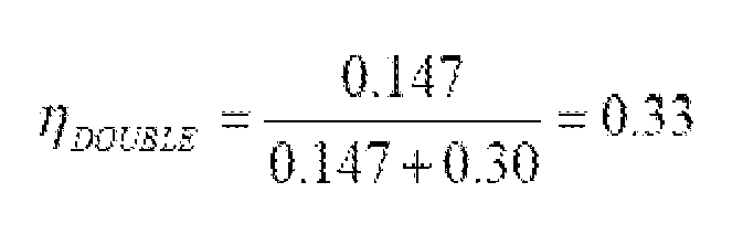
- Therefore, the efficiency η DOUBLE of the double-
track antenna 20 is considerably greater with respect to the efficiency η SINGLE of the single-track antenna 10. - In
Figure 2 , the double-track antenna 20 is also schematically represented without showing the PCB on which theturns corresponding tracks path 26, which is destined to pass through a suitable via-hole provided in the PCB. As will be illustrated better with reference toFigure 3 , theturns path 26. -
Figure 3 shows in greater detail anembodiment 50 of the double-track antenna 20 inFigure 2 . ThusFigure 3 shows an exploded view of an automotive key head, indicated in its entirety withreference 30, including an upper half-body 31 and a lower half-body 32, destined, along with an interposedrubber gasket 33 for sealing purposes, to be coupled together to house thePCB 35 inside of them. Such PCB 35 includes a plurality ofelectronic components 36, both discrete components such as resistors or condensers, or integrated circuits such as amplifiers, arranged on asubstrate 40, which realise a signal transmission circuit on a printed circuit board. -
Figures 4a and 4b represent in plan views of a firstupper face 37a ofsuch PCB 35 having serigraphed firstelectrical connection tracks 38a for suchelectronic components 36, and of asecond face 37b ofsuch PCB 35 having serigraphed secondelectrical connection tracks 38b, respectively. As can be noted inFigure 3 , both thefirst face 37a and thesecond face 37b haveperimetral tracks tracks Figure 2 . However, suchperimetral tracks substrate 40, rectangular, but having a pattern adapted to the shape of the housing defined by the half-bodies perimetral tracks hole 57. - Naturally, without prejudice to the underlying principle of the invention, the details and the embodiments may vary, even appreciably, with respect to what has been described and illustrated by way of example only, without departing from the scope of the present invention.
Claims (7)
- An antenna apparatus on a printed circuit board, including at least one printed circuit board (35), said printed circuit board (35) including a substrate (40) and a first printed metallic track (24; 54) on a first face (37a) of said substrate (40), said first printed metallic track (24; 54) being arranged prevalently along a perimeter of said substrate (40) and being configured as a loop antenna,
characterised in that
it includes at least a second track (25; 55) obtained on a second face (37b) of said substrate, said second track (25; 55) being arranged prevalently along the perimeter of said substrate (40) and configured as a second turn (23) of said loop antenna to which it is electrically connected by a viua-hole (27; 57) provided in said substrate (40) of said printed circuit board (35). - An apparatus according to claim 1, characterised in that said second track (25; 55) arranged prevalently along the perimeter of said substrate (40) is substantially congruent with said first track (24; 54) arranged prevalently along the perimeter of said substrate (40).
- An apparatus according to claim 2, characterised in that said second track (25; 55) lies in a plane substantially parallel to the plane in which said first track (24; 54) lies.
- An apparatus according to one or more of the previous claims, characterised in that said first track (24; 54) and said second track (25; 55) have a substantially rectangular shape.
- An apparatus according to one or more of the previous claims, characterised in that it is operatively associated with a signal transmission circuit (36) arranged on said PCB (35).
- An apparatus according to one or more of the previous claims, characterised in that it is included in a remote control device (30) for actuators.
- An apparatus according to the previous claim, characterised in that it is included in a body (31, 32) being part of an automobile key.
Priority Applications (1)
| Application Number | Priority Date | Filing Date | Title |
|---|---|---|---|
| EP08425347A EP2120289A1 (en) | 2008-05-16 | 2008-05-16 | Antenna apparatus on a printed circuit board |
Applications Claiming Priority (1)
| Application Number | Priority Date | Filing Date | Title |
|---|---|---|---|
| EP08425347A EP2120289A1 (en) | 2008-05-16 | 2008-05-16 | Antenna apparatus on a printed circuit board |
Publications (1)
| Publication Number | Publication Date |
|---|---|
| EP2120289A1 true EP2120289A1 (en) | 2009-11-18 |
Family
ID=39768555
Family Applications (1)
| Application Number | Title | Priority Date | Filing Date |
|---|---|---|---|
| EP08425347A Withdrawn EP2120289A1 (en) | 2008-05-16 | 2008-05-16 | Antenna apparatus on a printed circuit board |
Country Status (1)
| Country | Link |
|---|---|
| EP (1) | EP2120289A1 (en) |
Cited By (3)
| Publication number | Priority date | Publication date | Assignee | Title |
|---|---|---|---|---|
| WO2013098151A1 (en) * | 2011-12-29 | 2013-07-04 | Continental Automotive Gmbh | Transmission arrangement for a radio station and radio station |
| EP2466554A3 (en) * | 2010-12-15 | 2013-11-27 | Huf Hülsbeck & Fürst GmbH & Co. KG | Mobile ID transmitter for keyless systems |
| DE102013114223A1 (en) * | 2013-12-06 | 2015-06-11 | Hörmann KG Antriebstechnik | REMOTE CONTROL DOOR OR DOOR DRIVE WITH MAGNETIC ANTENNA |
Citations (4)
| Publication number | Priority date | Publication date | Assignee | Title |
|---|---|---|---|---|
| EP0674354A2 (en) * | 1994-03-24 | 1995-09-27 | Hochiki Corporation | Wireless access control system using a proximity member and antenna equipment therefor |
| EP1217685A2 (en) * | 2000-12-12 | 2002-06-26 | Matsushita Electric Industrial Co., Ltd. | Ring resonator and antenna |
| WO2005081808A1 (en) * | 2004-02-20 | 2005-09-09 | 3M Innovative Properties Company | Multi-loop antenna for radio frequency identification (rfid) communication |
| US20070241986A1 (en) * | 2006-04-13 | 2007-10-18 | Electronics And Telecommunications Research Institute | Windmill-shaped loop antenna having parasitic loop antenna |
-
2008
- 2008-05-16 EP EP08425347A patent/EP2120289A1/en not_active Withdrawn
Patent Citations (4)
| Publication number | Priority date | Publication date | Assignee | Title |
|---|---|---|---|---|
| EP0674354A2 (en) * | 1994-03-24 | 1995-09-27 | Hochiki Corporation | Wireless access control system using a proximity member and antenna equipment therefor |
| EP1217685A2 (en) * | 2000-12-12 | 2002-06-26 | Matsushita Electric Industrial Co., Ltd. | Ring resonator and antenna |
| WO2005081808A1 (en) * | 2004-02-20 | 2005-09-09 | 3M Innovative Properties Company | Multi-loop antenna for radio frequency identification (rfid) communication |
| US20070241986A1 (en) * | 2006-04-13 | 2007-10-18 | Electronics And Telecommunications Research Institute | Windmill-shaped loop antenna having parasitic loop antenna |
Cited By (6)
| Publication number | Priority date | Publication date | Assignee | Title |
|---|---|---|---|---|
| EP2466554A3 (en) * | 2010-12-15 | 2013-11-27 | Huf Hülsbeck & Fürst GmbH & Co. KG | Mobile ID transmitter for keyless systems |
| WO2013098151A1 (en) * | 2011-12-29 | 2013-07-04 | Continental Automotive Gmbh | Transmission arrangement for a radio station and radio station |
| US9524602B2 (en) | 2011-12-29 | 2016-12-20 | Continental Automotive Gmbh | Compact antenna structure with a coupling device |
| DE102013114223A1 (en) * | 2013-12-06 | 2015-06-11 | Hörmann KG Antriebstechnik | REMOTE CONTROL DOOR OR DOOR DRIVE WITH MAGNETIC ANTENNA |
| DE102013114223B4 (en) | 2013-12-06 | 2021-08-05 | Hörmann KG Antriebstechnik | REMOTE CONTROLLED DOOR OR DRIVE DEVICE WITH MAGNETIC ANTENNA |
| DE102013114223C5 (en) * | 2013-12-06 | 2026-02-19 | Hörmann KG Antriebstechnik | Remote Controlled Door or Gate Operator Device with Magnetic Antenna |
Similar Documents
| Publication | Publication Date | Title |
|---|---|---|
| US11133594B2 (en) | System and method with multilayer laminated waveguide antenna | |
| US7330161B2 (en) | Antenna, radio device, method of designing antenna, and method of measuring operating frequency of antenna | |
| EP3398228B1 (en) | A low thermal impedance structure in a phased array | |
| US8810457B2 (en) | Orthogonal modular embedded antenna, with method of manufacture and kits therefor | |
| JP5967290B2 (en) | High frequency transmission line | |
| EP3449532A1 (en) | Component carrier with integrated antenna arrangement, electronic apparatus, radio communication method | |
| CA2525620A1 (en) | Embedded rf vertical interconnect for flexible conformal antenna | |
| US10971806B2 (en) | Broadband conformal antenna | |
| JPWO2016203842A1 (en) | Electronic device and antenna element | |
| US9401533B2 (en) | Flat cable | |
| US20080315977A1 (en) | Low loss RF transmission lines | |
| US20140354486A1 (en) | Orthogonal modular embedded antenna, with method of manufacture and kits therefor | |
| WO2010013610A1 (en) | Planar antenna | |
| US9312590B2 (en) | High-frequency signal transmission line and electronic device | |
| KR20130111238A (en) | Sandwich structure for directional coupler | |
| CN114144945A (en) | Flexible cable | |
| US9318786B2 (en) | High-frequency signal line and electronic device | |
| WO2014157031A1 (en) | High-frequency transmission line and electronic device | |
| US20150022288A1 (en) | High-frequency signal line | |
| US9019048B1 (en) | High-frequency signal transmission line and electronic device | |
| CN202454710U (en) | Nondispersive delay line | |
| CN101997564A (en) | multi-antenna communication device | |
| JP2005236154A (en) | Electronic equipment | |
| CN118281563A (en) | Antenna components and electronic devices | |
| CN102496767A (en) | Non-dispersive delay line |
Legal Events
| Date | Code | Title | Description |
|---|---|---|---|
| PUAI | Public reference made under article 153(3) epc to a published international application that has entered the european phase |
Free format text: ORIGINAL CODE: 0009012 |
|
| AK | Designated contracting states |
Kind code of ref document: A1 Designated state(s): AT BE BG CH CY CZ DE DK EE ES FI FR GB GR HR HU IE IS IT LI LT LU LV MC MT NL NO PL PT RO SE SI SK TR |
|
| AX | Request for extension of the european patent |
Extension state: AL BA MK RS |
|
| AKX | Designation fees paid | ||
| REG | Reference to a national code |
Ref country code: DE Ref legal event code: 8566 |
|
| STAA | Information on the status of an ep patent application or granted ep patent |
Free format text: STATUS: THE APPLICATION IS DEEMED TO BE WITHDRAWN |
|
| 18D | Application deemed to be withdrawn |
Effective date: 20100519 |