EP2120287A1 - Antenna device - Google Patents
Antenna device Download PDFInfo
- Publication number
- EP2120287A1 EP2120287A1 EP08103991A EP08103991A EP2120287A1 EP 2120287 A1 EP2120287 A1 EP 2120287A1 EP 08103991 A EP08103991 A EP 08103991A EP 08103991 A EP08103991 A EP 08103991A EP 2120287 A1 EP2120287 A1 EP 2120287A1
- Authority
- EP
- European Patent Office
- Prior art keywords
- radiating element
- antenna device
- section
- parasitic
- connection point
- Prior art date
- Legal status (The legal status is an assumption and is not a legal conclusion. Google has not performed a legal analysis and makes no representation as to the accuracy of the status listed.)
- Withdrawn
Links
- 230000005684 electric field Effects 0.000 claims abstract description 22
- 238000010295 mobile communication Methods 0.000 claims abstract description 19
- 230000003071 parasitic effect Effects 0.000 claims description 38
- 230000000694 effects Effects 0.000 description 3
- 238000010521 absorption reaction Methods 0.000 description 2
- 230000008901 benefit Effects 0.000 description 2
- 230000007704 transition Effects 0.000 description 2
- 230000003247 decreasing effect Effects 0.000 description 1
- 230000001419 dependent effect Effects 0.000 description 1
- 238000010586 diagram Methods 0.000 description 1
- 238000011038 discontinuous diafiltration by volume reduction Methods 0.000 description 1
- 238000000034 method Methods 0.000 description 1
- 230000001603 reducing effect Effects 0.000 description 1
- 125000006850 spacer group Chemical group 0.000 description 1
Images


Classifications
-
- H—ELECTRICITY
- H01—ELECTRIC ELEMENTS
- H01Q—ANTENNAS, i.e. RADIO AERIALS
- H01Q1/00—Details of, or arrangements associated with, antennas
- H01Q1/12—Supports; Mounting means
- H01Q1/22—Supports; Mounting means by structural association with other equipment or articles
- H01Q1/24—Supports; Mounting means by structural association with other equipment or articles with receiving set
- H01Q1/241—Supports; Mounting means by structural association with other equipment or articles with receiving set used in mobile communications, e.g. GSM
- H01Q1/242—Supports; Mounting means by structural association with other equipment or articles with receiving set used in mobile communications, e.g. GSM specially adapted for hand-held use
- H01Q1/243—Supports; Mounting means by structural association with other equipment or articles with receiving set used in mobile communications, e.g. GSM specially adapted for hand-held use with built-in antennas
-
- H—ELECTRICITY
- H01—ELECTRIC ELEMENTS
- H01Q—ANTENNAS, i.e. RADIO AERIALS
- H01Q9/00—Electrically-short antennas having dimensions not more than twice the operating wavelength and consisting of conductive active radiating elements
- H01Q9/04—Resonant antennas
- H01Q9/0407—Substantially flat resonant element parallel to ground plane, e.g. patch antenna
- H01Q9/0471—Non-planar, stepped or wedge-shaped patch
Definitions
- the present invention generally relates to antenna devices and in particular to reducing effect of nearby objects of antenna devices.
- Planar antennas have found a widespread use in many fields, such as for mobile communication.
- a conventional planar antenna is shown in Fig 1 .
- the antenna device 1 has conducting surface of a radiating element 3 is provided spaced apart from a ground plane 6 in the form of a large conducting surface and with air between the conducting surface and the ground plane. Spacers can be used to fix the position of the radiating element 3 in an essentially parallel position in relation to the ground plane 6.
- the radiating element 3 is connected at a connection point 4 to a signal source 7.
- a slit 5 By means of a slit 5, several resistive paths of different lengths are provided from the connection point 4, for example creating a low band (LB) section and a high band (HB) section of the radiating element 3.
- LB low band
- HB high band
- a parasitic element 10 is often provided to improve performance of the antenna device 1.
- the parasitic element 10 is connected to ground at a ground connection point 11.
- Fig 2 shows a typical position of an antenna device in a mobile communication terminal 40.
- the ground plane 6 is relatively large and the radiating element 3 is relatively small.
- the radiating element 3 is located close to the casing of the mobile communication terminal 40.
- the radiating element 3 is located close to a rear surface 43 of the mobile communication terminal 40.
- the rear surface 43 is opposite the front surface 44, where display 41, keypad 42, etc. are provided.
- a problem occurs when a part of a user's body, such as a finger is placed close to the radiating element 3 of the mobile terminal 40. Due to the proximity of the finger to the radiating element 3, performance of the antenna is decreased. Since the presence of fingers is very common whenever the user uses the mobile communication terminal for voice calls, unless a hands-free unit is used, such a situation would greatly benefit from any performance improvements.
- the American patent application with publication number US2007/0241977 presents position sensors for detecting the position of the user's hand on the housing.
- the output signals from the sensors are used by a controller to adjust the source impedance of the transmitter and/or receiver based on the position of the user's hand to match the antenna impedance.
- an objective of the present invention is to alleviate the problem of reduced performance when a finger is placed near an antenna device.
- the above objectives are achieved by the attached independent patent claims.
- an antenna device for a mobile communication terminal comprising: a radiating element and a connection point on the radiating element.
- the radiating element comprises at least one section arranged at a position which comprises an area of the radiating element with an electric field which is, when the antenna device is in use, stronger than an average electric field of the radiating element.
- the at least one section is arranged closer to a ground plane of the mobile communication terminal than other parts of the radiating element, and the at least one section is essentially parallel to the ground plane.
- At least one section of the radiating element is provided at a larger distance from the casing of the mobile communication terminal.
- the at least one section may comprise an area of the radiating element with an electric field which is, when the antenna device is in use, stronger than any other area of the radiating element.
- a shortest distance between the ground plane and the at least one section may be less than nine tenths of a shortest distance between the ground plane and the other parts of the radiating element.
- the at least one section may comprise an end section of the radiating element, wherein the end section has an average resistive path to the connection point which is longer than an average resistive path to the connection point of one other end sections of the radiating element.
- connection point is not a zero dimensional point; it is a two dimensional connection area of the radiating element, but since its area is small in relation to the radiating element, it is conveniently called a connection point.
- the at least one section may comprise an end section of the radiating element, wherein the end section has an average resistive path to the connection point which is longer than average resistive paths to the connection point of all other end sections of the radiating element.
- a shortest resistive distance from a free end of the end section to the other parts of the radiating element may be at least one tenth of a shortest resistive distance from the free end to the connection point.
- the end section may be of rectangular shape.
- the radiating element may comprise a slit and the at least one section may comprise two sections at opposite sides of the slit, by an opening of the slit.
- the antenna device may further comprise a parasitic element with a ground connection point.
- the parasitic element may comprise a parasitic end section arranged at a position which comprises an area of the parasitic element with an electric field which is, when the antenna device is in use, stronger than an average electric field of the parasitic element, and the parasitic end section may be arranged closer to the ground plane of the mobile communication terminal than other parts of the parasitic element, and the parasitic end section is essentially parallel to the ground plane.
- ground connection point is not a zero dimensional point; it is a two dimensional connection area of the radiating element, but since its area is small in relation to the radiating element, it is conveniently called a ground connection point.
- the parasitic end section may have an average resistive path to the ground connection point which is longer than an average resistive path to the ground connection point of another end section of the radiating element.
- the parasitic end section may have an average resistive path to the ground connection point which is longer than average resistive paths to the ground connection point of all other end sections of the parasitic element.
- a shortest resistive distance from a free end of the parasitic end section to the other parts of the parasitic element may be at least one tenth of a shortest resistive distance from the free end of the parasitic end section to the ground connection point.
- a second aspect of the invention is a mobile communication terminal comprising an antenna device according to the first aspect.
- Fig 3 is a graph showing total and impedance mismatch loss in relation to various finger positions with an antenna device such as the antenna device 1 of Fig 1 .
- the x axis represents frequency and the y axis represents loss in dB.
- the x axis is divided into two parts for two commonly used frequency ranges around 900 MHz and 1800 MHz, respectively.
- Solid lines 54a-d represent when a finger is placed on a high band (HB) portion of the antenna device. There is of course a casing between the actual radiating element of the antenna device and the finger. Nevertheless, the actual distance is still small in relation to the planar dimensions of the antenna device.
- Dashed lines 55a-d represent when a finger is placed on a centre portion of the antenna device and dotted lines 56a-d represent when a finger is placed on a low band portion of the antenna device.
- the upper lines 54a, 55a, 56a there are substantial total losses in the frequency range of 870 - 1000 MHz.
- the lower lines 54b, 55b, 56b represent losses that are due to mismatched impedances. At least in theory, the mismatched losses can be eliminated with perfectly matched impedances. Nevertheless, even if the mismatch losses are completely eliminated, there is still a large loss remaining, represented by the difference between the lower lines 54b, 55b, 56b, representing the impedance mismatch losses for the respective finger positions, and the upper lines 54a, 55a, 56a, representing the total losses for the respective finger positions. This remaining loss is in the range of 12 to 14 dB for the lower frequency range.
- the sections that are lowered towards the ground plane 6 should be significant enough in size to produce such an effect.
- the sections may be provided such that they are kept essentially parallel to the ground plate, but at a level closer to the ground plate than other parts of the radiating element 3.
- Figs 4 to 6 are schematic diagrams showing various embodiments of the present invention where different sections are lowered towards the ground plane.
- Fig 4 it is shown how an end section 21 is lowered in relation to the ground plane.
- the end section 21 is the end section with the greatest average resistive path to the connection point 4.
- the radiating element 3 has a free end 28 being the end with the longest average resistive distance to the connection point 4.
- a shortest resistive distance from the free end 28 to other parts (which are not lowered) of the radiating element 3, is at least a fraction of a shortest resistive distance from the free end 28 to the connection point 4.
- the fraction can for example be a tenth, an eighth or a quarter.
- the resistive distance to the section 21 is long from the connection point 4, the electrical field is high in this region. Consequently, by lowering this end section 21 towards the ground plane, the physical distance to the casing and therefore any finger on the casing is increased. Losses due to finger placement, e.g. due to absorption of electrical field by the finger, is thereby reduced.
- Fig 5 two sections 20a and 20b are lowered towards the ground plane. It has been found that sections 20a and 20b, opposite each other by the opening of the slit 5, generate a high electrical field. The shortest resistive path between these two sections 20a and 20b is relatively large. Hence, by lowering these sections 20a and 20b towards the ground plane, losses due to finger placement is reduced.
- a parasitic end section 22 of the parasitic element 10 is lowered towards the ground plane.
- This section is the end section of the parasitic element 10 with the greatest resistive path to the ground connection point 11.
- the parasitic end section 22 of the parasitic element 10 has a free end 24 which is the end with the longest average resistive distance to the ground connection point 11.
- a shortest resistive distance 25 from the free end 24 to other parts (which are not lowered) of the parasitic element is at least a fraction of a shortest resistive distance 26 from the free end 24 to the ground connection point 11.
- the fraction can for example be a tenth, an eighth or a quarter. Since the electrical field is relatively high in the region around the end section 22 of the parasitic element 10 and this section 22 is lowered towards the ground plane, losses due to finger placement is reduced.
- a section 23 adjacent to one section 20b by the entrance of the slit can also be lowered.
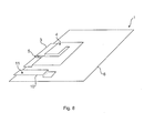
- Fig 8 is a perspective view of the embodiment shown in Fig 7 .
- all dashed areas 22, 21, 20a, 20b, 23 are lowered towards the ground plane 6.
- this is a mere schematic illustration. More specifically, the size and shape of the lowered sections 22, 21, 20a, 20b, 23 can be varied as desired.
- the transition from a lowered section to other, not lowered sections is not necessarily a straight fold as shown here. The transition can also be slanted or of a more rounded shape.
Landscapes
- Engineering & Computer Science (AREA)
- Computer Networks & Wireless Communication (AREA)
- Support Of Aerials (AREA)
Abstract
Description
- The present invention generally relates to antenna devices and in particular to reducing effect of nearby objects of antenna devices.
- Planar antennas have found a widespread use in many fields, such as for mobile communication. A conventional planar antenna is shown in
Fig 1 . Theantenna device 1 has conducting surface of a radiatingelement 3 is provided spaced apart from aground plane 6 in the form of a large conducting surface and with air between the conducting surface and the ground plane. Spacers can be used to fix the position of theradiating element 3 in an essentially parallel position in relation to theground plane 6. The radiatingelement 3 is connected at aconnection point 4 to a signal source 7. By means of aslit 5, several resistive paths of different lengths are provided from theconnection point 4, for example creating a low band (LB) section and a high band (HB) section of theradiating element 3. Hence, several sets of frequencies can be tuned to. As is known in the art, aparasitic element 10 is often provided to improve performance of theantenna device 1. Theparasitic element 10 is connected to ground at aground connection point 11. -
Fig 2 shows a typical position of an antenna device in amobile communication terminal 40. Theground plane 6 is relatively large and theradiating element 3 is relatively small. The radiatingelement 3 is located close to the casing of themobile communication terminal 40. Typically, the radiatingelement 3 is located close to arear surface 43 of themobile communication terminal 40. Therear surface 43 is opposite thefront surface 44, wheredisplay 41,keypad 42, etc. are provided. - A problem occurs when a part of a user's body, such as a finger is placed close to the
radiating element 3 of themobile terminal 40. Due to the proximity of the finger to theradiating element 3, performance of the antenna is decreased. Since the presence of fingers is very common whenever the user uses the mobile communication terminal for voice calls, unless a hands-free unit is used, such a situation would greatly benefit from any performance improvements. - The American patent application with publication number
US2007/0241977 presents position sensors for detecting the position of the user's hand on the housing. The output signals from the sensors are used by a controller to adjust the source impedance of the transmitter and/or receiver based on the position of the user's hand to match the antenna impedance. - While such a solution is to some extent reduces the negative effect of the presence of the fingers or hand, the effects are not eliminated.
- Consequently, there is a need for an antenna device with improved performance in the presence of hands or fingers.
- In view of the above, an objective of the present invention is to alleviate the problem of reduced performance when a finger is placed near an antenna device. Generally, the above objectives are achieved by the attached independent patent claims.
- According to a first aspect of the present invention it is provided an antenna device for a mobile communication terminal comprising: a radiating element and a connection point on the radiating element. The radiating element comprises at least one section arranged at a position which comprises an area of the radiating element with an electric field which is, when the antenna device is in use, stronger than an average electric field of the radiating element. Furthermore, the at least one section is arranged closer to a ground plane of the mobile communication terminal than other parts of the radiating element, and the at least one section is essentially parallel to the ground plane.
- In other words, at least one section of the radiating element is provided at a larger distance from the casing of the mobile communication terminal. By providing sections of the radiating element, where the electrical field is high, closer to the ground plane, the losses due to finger placement are reduced. This results in a reduction in power use and/or improved reception with the antenna device. Since larger volume, as defined by the radiating element and the ground place, are better in terms of bandwidth and gain, there is a driving force within the prior art to keep the volume as large as possible, only restricted by physical constraints of the mobile communication terminal. Furthermore, the introduction of this invention still allows for excellent free space performance.
- The at least one section may comprise an area of the radiating element with an electric field which is, when the antenna device is in use, stronger than any other area of the radiating element.
- A shortest distance between the ground plane and the at least one section may be less than nine tenths of a shortest distance between the ground plane and the other parts of the radiating element.
- The at least one section may comprise an end section of the radiating element, wherein the end section has an average resistive path to the connection point which is longer than an average resistive path to the connection point of one other end sections of the radiating element.
- It has been found that the electrical field is relatively high at such an end section where a voltage difference in relation to the connection point is relatively large. It is to be noted that the connection point is not a zero dimensional point; it is a two dimensional connection area of the radiating element, but since its area is small in relation to the radiating element, it is conveniently called a connection point.
- The at least one section may comprise an end section of the radiating element, wherein the end section has an average resistive path to the connection point which is longer than average resistive paths to the connection point of all other end sections of the radiating element.
- A shortest resistive distance from a free end of the end section to the other parts of the radiating element may be at least one tenth of a shortest resistive distance from the free end to the connection point.
- The end section may be of rectangular shape.
- The radiating element may comprise a slit and the at least one section may comprise two sections at opposite sides of the slit, by an opening of the slit.
- By the opening of a slit, there is a relatively large difference in voltage, resulting in a relatively large electrical field.
- The antenna device may further comprise a parasitic element with a ground connection point. The parasitic element may comprise a parasitic end section arranged at a position which comprises an area of the parasitic element with an electric field which is, when the antenna device is in use, stronger than an average electric field of the parasitic element, and the parasitic end section may be arranged closer to the ground plane of the mobile communication terminal than other parts of the parasitic element, and the parasitic end section is essentially parallel to the ground plane.
- It is to be noted that the ground connection point is not a zero dimensional point; it is a two dimensional connection area of the radiating element, but since its area is small in relation to the radiating element, it is conveniently called a ground connection point.
- The parasitic end section may have an average resistive path to the ground connection point which is longer than an average resistive path to the ground connection point of another end section of the radiating element. Alternatively, or additionally, the parasitic end section may have an average resistive path to the ground connection point which is longer than average resistive paths to the ground connection point of all other end sections of the parasitic element.
- A shortest resistive distance from a free end of the parasitic end section to the other parts of the parasitic element may be at least one tenth of a shortest resistive distance from the free end of the parasitic end section to the ground connection point.
- A second aspect of the invention is a mobile communication terminal comprising an antenna device according to the first aspect.
- Other objectives, features and advantages of the present invention will appear from the following detailed description, from the appended dependent claims as well as from the drawings.
- Generally, all terms used in the claims are to be interpreted according to their ordinary meaning in the technical field, unless explicitly defined otherwise herein. All references to "a/an/the element, device, component, means, step, etc" are to be interpreted openly as referring to at least one instance of the element, device, component, means, step, etc., unless explicitly stated otherwise. The steps of any method disclosed herein do not have to be performed in the exact order disclosed, unless explicitly stated.
- The invention is now described, by way of example, with reference to the accompanying drawings, in which:
-
Fig 1 is a schematic perspective view of a conventional antenna device; -
Fig 2 is a schematic side view showing the position of the antenna device ofFig 1 in a mobile communication terminal; -
Fig 3 is a graph showing total and impedance mismatch loss with various finger positions with an antenna device such as the antenna device ofFig 1 ; -
Fig 4 is a plan view of an embodiment of the present invention where an end section of a radiating element is lowered; -
Fig 5 is a plan view of an embodiment of the present invention where opposite sections by an opening of a slit of a radiating element are lowered; -
Fig 6 is a plan view of an embodiment of the present invention where an end section of a parasitic element is lowered; -
Fig 7 is a plan view of an embodiment of the present invention being a combination of the embodiments ofFigs 4 to 6 ; and -
Fig 8 is a perspective view of an embodiment of the present invention being a combination of the embodiments ofFigs 4 to 6 . - The present invention will now be described more fully hereinafter with reference to the accompanying drawings, in which certain embodiments of the invention are shown. This invention may, however, be embodied in many different forms and should not be construed as limited to the embodiments set forth herein; rather, these embodiments are provided by way of example so that this disclosure will be thorough and complete, and will fully convey the scope of the invention to those skilled in the art. Like numbers refer to like elements throughout the description.
-
Fig 3 is a graph showing total and impedance mismatch loss in relation to various finger positions with an antenna device such as theantenna device 1 ofFig 1 . The x axis represents frequency and the y axis represents loss in dB. The x axis is divided into two parts for two commonly used frequency ranges around 900 MHz and 1800 MHz, respectively.Solid lines 54a-d represent when a finger is placed on a high band (HB) portion of the antenna device. There is of course a casing between the actual radiating element of the antenna device and the finger. Nevertheless, the actual distance is still small in relation to the planar dimensions of the antenna device. Dashedlines 55a-d represent when a finger is placed on a centre portion of the antenna device and dottedlines 56a-d represent when a finger is placed on a low band portion of the antenna device. - As can be seen by the
upper lines lower lines lower lines upper lines - With reference to
Fig 1 , by providing sections of the radiatingelement 3, where the electrical field is high, closer to theground plane 6, the losses due to finger placement are reduced. The sections that are lowered towards theground plane 6 should be significant enough in size to produce such an effect. For example, the sections may be provided such that they are kept essentially parallel to the ground plate, but at a level closer to the ground plate than other parts of the radiatingelement 3. - However, performance, and particularly bandwidth, of the antenna device is improved with a greater total volume as defined by the radiating
element 3 and the ground plane. Therefore, for example, if the whole radiating element is lowered towards the ground plane, losses due to finger placement are indeed reduced, but at the cost of significant reduction of bandwidth. Hence, it is desired to lower only those parts of the radiating element where the electrical field is high relative to other parts of the radiating element. In this way, losses due to finger placement are reduced, but without affecting bandwidth a great deal, or at least at an acceptable level. -
Figs 4 to 6 are schematic diagrams showing various embodiments of the present invention where different sections are lowered towards the ground plane. - In
Fig 4 , it is shown how anend section 21 is lowered in relation to the ground plane. Theend section 21 is the end section with the greatest average resistive path to theconnection point 4. The radiatingelement 3 has afree end 28 being the end with the longest average resistive distance to theconnection point 4. In one embodiment, a shortest resistive distance from thefree end 28 to other parts (which are not lowered) of the radiatingelement 3, is at least a fraction of a shortest resistive distance from thefree end 28 to theconnection point 4. The fraction can for example be a tenth, an eighth or a quarter. - Since the resistive distance to the
section 21 is long from theconnection point 4, the electrical field is high in this region. Consequently, by lowering thisend section 21 towards the ground plane, the physical distance to the casing and therefore any finger on the casing is increased. Losses due to finger placement, e.g. due to absorption of electrical field by the finger, is thereby reduced. - In
Fig 5 , twosections sections slit 5, generate a high electrical field. The shortest resistive path between these twosections sections - In
Fig 6 , aparasitic end section 22 of theparasitic element 10 is lowered towards the ground plane. This section is the end section of theparasitic element 10 with the greatest resistive path to theground connection point 11. Theparasitic end section 22 of theparasitic element 10 has afree end 24 which is the end with the longest average resistive distance to theground connection point 11. In one embodiment, a shortest resistive distance 25 from thefree end 24 to other parts (which are not lowered) of the parasitic element, is at least a fraction of a shortestresistive distance 26 from thefree end 24 to theground connection point 11. The fraction can for example be a tenth, an eighth or a quarter. Since the electrical field is relatively high in the region around theend section 22 of theparasitic element 10 and thissection 22 is lowered towards the ground plane, losses due to finger placement is reduced. - The embodiments illustrated in
Figs 4-6 above can be freely be combined to achieve desired combination of reduced loss due to finger placement and volume reduction, as defined by the radiating element and the ground plate. - For example, as shown in
Fig 7 , all lowered elements ofFigs 4-6 are combined in one embodiment. Here, theend section 22 of the parasitic element, theend section 21 of the radiating element and the opposingsections slit 5 are all lowered. In this embodiment there is an overlap of the end section of the radiatingelement 3 and onesection 20a by the entrance of the slit. However, this is not an issue, since both thesesections - To simplify production, a
section 23 adjacent to onesection 20b by the entrance of the slit can also be lowered. -
Fig 8 is a perspective view of the embodiment shown inFig 7 . As can be seen, all dashedareas ground plane 6. It is to be noted that this is a mere schematic illustration. More specifically, the size and shape of the loweredsections - The invention has mainly been described above with reference to a few embodiments. However, as is readily appreciated by a person skilled in the art, other embodiments than the ones disclosed above are equally possible within the scope of the invention, as defined by the appended patent claims.
Claims (12)
- An antenna device (1) for a mobile communication terminal comprising:a radiating element (3); anda connection point (4) on said radiating element (3);characterised in that
said radiating element (3) comprises at least one section (21, 20a, 20b) arranged at a position which comprises an area of said radiating element (3) with an electric field which is, when said antenna device is in use, stronger than an average electric field of said radiating element (3); and
said at least one section (21, 20a, 20b) is arranged closer to a ground plane (6) of said mobile communication terminal than other parts of said radiating element (3), and said at least one section (21, 20a, 20b) is essentially parallel to said ground plane (6). - The antenna device according to claim 1, wherein said at least one section (21, 20a, 20b) comprises an area of said radiating element (3) with an electric field which is stronger than any other area of said radiating element (3).
- The antenna device according to claim 1 or 2, wherein a shortest distance between said ground plane (6) and said at least one section (21, 20a, 20b) is less than nine tenths of a shortest distance between said ground plane (6) and said other parts of said radiating element (3).
- The antenna device according to any one of claims 1 to 3, wherein said at least one section comprises an end section (21) of said radiating element, wherein said end section (21) has an average resistive path to said connection point (4) which is longer than an average resistive path to said connection point (4) of one other end sections of said radiating element.
- The antenna device according to any one of claims 1 to 4, wherein said at least one section comprises an end section (21) of said radiating element, wherein said end section (21) has an average resistive path to said connection point (4) which is longer than average resistive paths to said connection point (4) of all other end sections of said radiating element.
- The antenna device according to claim 4 or 5, wherein a shortest resistive distance from a free end (28) of said end section to said other parts of said radiating element is at least one tenth of a shortest resistive distance from said free end (28) to said connection point (4).
- The antenna device according to any one of claims 4 to 6, wherein said end section (21) is of rectangular shape.
- The antenna device according to any one of the previous claims, wherein said radiating element comprises a slit (5) and said at least one section comprises two sections (20a, 20b) at opposite sides of said slit, by an opening of said slit (5).
- The antenna device according to any one of the previous claims, wherein:said antenna device further comprises a parasitic element (10) with a ground connection point (11),said parasitic element (10) comprises a parasitic end section (22) arranged at a position which comprises an area of said parasitic element (10) with an electric field which is, when said antenna device is in use, stronger than an average electric field of said parasitic element (10), andsaid parasitic end section (22) is arranged closer to said ground plane (6) of said mobile communication terminal than other parts of said parasitic element (10), and said parasitic end section (22) is essentially parallel to said ground plane (6).
- The antenna device according to claim 9, wherein said parasitic end section (22) has an average resistive path to said ground connection point (11) which is longer than an average resistive path to said ground connection point (11) of another end section of said parasitic element.
- The antenna device according to claim 10, wherein a shortest resistive distance from a free end (24) of said parasitic end section (22) to said other parts of said parasitic element (10) is at least one tenth of a shortest resistive distance from said free end (24) of said parasitic end section (22) to said ground connection point (11).
- A mobile communication terminal comprising a ground plane and an antenna device according to any one of the previous claims.
Priority Applications (2)
| Application Number | Priority Date | Filing Date | Title |
|---|---|---|---|
| EP08103991A EP2120287A1 (en) | 2008-05-16 | 2008-05-16 | Antenna device |
| PCT/SE2009/050544 WO2009139718A1 (en) | 2008-05-16 | 2009-05-14 | Improved antenna device and mobile communication terminal |
Applications Claiming Priority (1)
| Application Number | Priority Date | Filing Date | Title |
|---|---|---|---|
| EP08103991A EP2120287A1 (en) | 2008-05-16 | 2008-05-16 | Antenna device |
Publications (1)
| Publication Number | Publication Date |
|---|---|
| EP2120287A1 true EP2120287A1 (en) | 2009-11-18 |
Family
ID=39941587
Family Applications (1)
| Application Number | Title | Priority Date | Filing Date |
|---|---|---|---|
| EP08103991A Withdrawn EP2120287A1 (en) | 2008-05-16 | 2008-05-16 | Antenna device |
Country Status (2)
| Country | Link |
|---|---|
| EP (1) | EP2120287A1 (en) |
| WO (1) | WO2009139718A1 (en) |
Citations (5)
| Publication number | Priority date | Publication date | Assignee | Title |
|---|---|---|---|---|
| EP1052723A2 (en) * | 1999-05-10 | 2000-11-15 | Nokia Mobile Phones Ltd. | Antenna construction |
| WO2001033665A1 (en) * | 1999-11-04 | 2001-05-10 | Rangestar Wireless, Inc. | Single or dual band parasitic antenna assembly |
| US20050041624A1 (en) * | 2003-06-03 | 2005-02-24 | Ping Hui | Systems and methods that employ a dualband IFA-loop CDMA antenna and a GPS antenna with a device for mobile communication |
| US20060033667A1 (en) * | 2002-02-13 | 2006-02-16 | Greg Johnson | Oriented PIFA-type device and method of use for reducing RF interference |
| US20070241977A1 (en) | 2004-05-03 | 2007-10-18 | Sony Ericsson Mobile Communications Ab | Impedance Matching Circuit for a Mobile Communication Device |
Family Cites Families (2)
| Publication number | Priority date | Publication date | Assignee | Title |
|---|---|---|---|---|
| US20030210190A1 (en) * | 2002-05-07 | 2003-11-13 | Yi-Chang Lai | Dipole antenna structure |
| US7079077B2 (en) * | 2004-02-02 | 2006-07-18 | Southern Methodist University | Methods and apparatus for implementation of an antenna for a wireless communication device |
-
2008
- 2008-05-16 EP EP08103991A patent/EP2120287A1/en not_active Withdrawn
-
2009
- 2009-05-14 WO PCT/SE2009/050544 patent/WO2009139718A1/en not_active Ceased
Patent Citations (5)
| Publication number | Priority date | Publication date | Assignee | Title |
|---|---|---|---|---|
| EP1052723A2 (en) * | 1999-05-10 | 2000-11-15 | Nokia Mobile Phones Ltd. | Antenna construction |
| WO2001033665A1 (en) * | 1999-11-04 | 2001-05-10 | Rangestar Wireless, Inc. | Single or dual band parasitic antenna assembly |
| US20060033667A1 (en) * | 2002-02-13 | 2006-02-16 | Greg Johnson | Oriented PIFA-type device and method of use for reducing RF interference |
| US20050041624A1 (en) * | 2003-06-03 | 2005-02-24 | Ping Hui | Systems and methods that employ a dualband IFA-loop CDMA antenna and a GPS antenna with a device for mobile communication |
| US20070241977A1 (en) | 2004-05-03 | 2007-10-18 | Sony Ericsson Mobile Communications Ab | Impedance Matching Circuit for a Mobile Communication Device |
Also Published As
| Publication number | Publication date |
|---|---|
| WO2009139718A1 (en) | 2009-11-19 |
Similar Documents
| Publication | Publication Date | Title |
|---|---|---|
| US8933849B2 (en) | Portable wireless device | |
| EP3930097B1 (en) | Three-slotted antenna apparatus and method | |
| US20120229348A1 (en) | Antenna structure and electronic device having the same | |
| US7342539B2 (en) | Wideband loop antenna | |
| US8068063B2 (en) | Dual-band coupling device comprising first and second annular grooves fed by first and second feed conductors | |
| US20100328164A1 (en) | Switched antenna with an ultra wideband feed element | |
| US8933852B2 (en) | Mobile communication device and antenna structure therein | |
| US8890762B2 (en) | Communication electronic device and antenna structure thereof | |
| US8217851B2 (en) | Dual band antenna | |
| US20140049431A1 (en) | Multi-band antenna | |
| US8223076B2 (en) | Minified dual-band printed monopole antenna | |
| CN1739218B (en) | Mobile communication terminal | |
| EP1416585B1 (en) | Wideband loop antenna | |
| JP5652133B2 (en) | Multi-antenna device and portable device | |
| CN101997162A (en) | Multi-frequency antenna | |
| JP5707501B2 (en) | ANTENNA DEVICE AND ANTENNA MOUNTING METHOD | |
| CN104167594A (en) | Broadband antenna and radio communication device applied with broadband antenna | |
| JP4413145B2 (en) | Portable wireless terminal device | |
| CN102142611A (en) | Dipole antenna | |
| EP2639881A1 (en) | Communication device and tunable antenna element therein | |
| WO2009139718A1 (en) | Improved antenna device and mobile communication terminal | |
| US20100315308A1 (en) | Multi-Band Antenna | |
| US8854263B2 (en) | Antenna structure and electronic device having the same | |
| US7397441B1 (en) | Antenna element for a portable communication device | |
| US8373606B2 (en) | Slim mobile communication device and antenna structure thereof |
Legal Events
| Date | Code | Title | Description |
|---|---|---|---|
| PUAI | Public reference made under article 153(3) epc to a published international application that has entered the european phase |
Free format text: ORIGINAL CODE: 0009012 |
|
| AK | Designated contracting states |
Kind code of ref document: A1 Designated state(s): AT BE BG CH CY CZ DE DK EE ES FI FR GB GR HR HU IE IS IT LI LT LU LV MC MT NL NO PL PT RO SE SI SK TR |
|
| AX | Request for extension of the european patent |
Extension state: AL BA MK RS |
|
| 17P | Request for examination filed |
Effective date: 20100503 |
|
| 17Q | First examination report despatched |
Effective date: 20100525 |
|
| AKX | Designation fees paid |
Designated state(s): DE FR GB |
|
| STAA | Information on the status of an ep patent application or granted ep patent |
Free format text: STATUS: THE APPLICATION IS DEEMED TO BE WITHDRAWN |
|
| 18D | Application deemed to be withdrawn |
Effective date: 20101005 |