EP2120259A1 - Ball-bump bonded ribbon-wire interconnect - Google Patents
Ball-bump bonded ribbon-wire interconnect Download PDFInfo
- Publication number
- EP2120259A1 EP2120259A1 EP09251320A EP09251320A EP2120259A1 EP 2120259 A1 EP2120259 A1 EP 2120259A1 EP 09251320 A EP09251320 A EP 09251320A EP 09251320 A EP09251320 A EP 09251320A EP 2120259 A1 EP2120259 A1 EP 2120259A1
- Authority
- EP
- European Patent Office
- Prior art keywords
- ribbon
- wire
- ball
- bump
- substrate
- Prior art date
- Legal status (The legal status is an assumption and is not a legal conclusion. Google has not performed a legal analysis and makes no representation as to the accuracy of the status listed.)
- Withdrawn
Links
Images

Classifications
-
- H—ELECTRICITY
- H10—SEMICONDUCTOR DEVICES; ELECTRIC SOLID-STATE DEVICES NOT OTHERWISE PROVIDED FOR
- H10W—GENERIC PACKAGES, INTERCONNECTIONS, CONNECTORS OR OTHER CONSTRUCTIONAL DETAILS OF DEVICES COVERED BY CLASS H10
- H10W72/00—Interconnections or connectors in packages
- H10W72/60—Strap connectors, e.g. thick copper clips for grounding of power devices
-
- H—ELECTRICITY
- H10—SEMICONDUCTOR DEVICES; ELECTRIC SOLID-STATE DEVICES NOT OTHERWISE PROVIDED FOR
- H10W—GENERIC PACKAGES, INTERCONNECTIONS, CONNECTORS OR OTHER CONSTRUCTIONAL DETAILS OF DEVICES COVERED BY CLASS H10
- H10W72/00—Interconnections or connectors in packages
- H10W72/071—Connecting or disconnecting
- H10W72/075—Connecting or disconnecting of bond wires
-
- H—ELECTRICITY
- H10—SEMICONDUCTOR DEVICES; ELECTRIC SOLID-STATE DEVICES NOT OTHERWISE PROVIDED FOR
- H10W—GENERIC PACKAGES, INTERCONNECTIONS, CONNECTORS OR OTHER CONSTRUCTIONAL DETAILS OF DEVICES COVERED BY CLASS H10
- H10W72/00—Interconnections or connectors in packages
- H10W72/071—Connecting or disconnecting
- H10W72/075—Connecting or disconnecting of bond wires
- H10W72/07511—Treating the bonding area before connecting, e.g. by applying flux or cleaning
-
- H—ELECTRICITY
- H10—SEMICONDUCTOR DEVICES; ELECTRIC SOLID-STATE DEVICES NOT OTHERWISE PROVIDED FOR
- H10W—GENERIC PACKAGES, INTERCONNECTIONS, CONNECTORS OR OTHER CONSTRUCTIONAL DETAILS OF DEVICES COVERED BY CLASS H10
- H10W72/00—Interconnections or connectors in packages
- H10W72/071—Connecting or disconnecting
- H10W72/075—Connecting or disconnecting of bond wires
- H10W72/07521—Aligning
-
- H—ELECTRICITY
- H10—SEMICONDUCTOR DEVICES; ELECTRIC SOLID-STATE DEVICES NOT OTHERWISE PROVIDED FOR
- H10W—GENERIC PACKAGES, INTERCONNECTIONS, CONNECTORS OR OTHER CONSTRUCTIONAL DETAILS OF DEVICES COVERED BY CLASS H10
- H10W72/00—Interconnections or connectors in packages
- H10W72/071—Connecting or disconnecting
- H10W72/075—Connecting or disconnecting of bond wires
- H10W72/07531—Techniques
- H10W72/07532—Compression bonding, e.g. thermocompression bonding
- H10W72/07533—Ultrasonic bonding, e.g. thermosonic bonding
-
- H—ELECTRICITY
- H10—SEMICONDUCTOR DEVICES; ELECTRIC SOLID-STATE DEVICES NOT OTHERWISE PROVIDED FOR
- H10W—GENERIC PACKAGES, INTERCONNECTIONS, CONNECTORS OR OTHER CONSTRUCTIONAL DETAILS OF DEVICES COVERED BY CLASS H10
- H10W72/00—Interconnections or connectors in packages
- H10W72/071—Connecting or disconnecting
- H10W72/075—Connecting or disconnecting of bond wires
- H10W72/07551—Connecting or disconnecting of bond wires characterised by changes in properties of the bond wires during the connecting
- H10W72/07553—Connecting or disconnecting of bond wires characterised by changes in properties of the bond wires during the connecting changes in shapes
-
- H—ELECTRICITY
- H10—SEMICONDUCTOR DEVICES; ELECTRIC SOLID-STATE DEVICES NOT OTHERWISE PROVIDED FOR
- H10W—GENERIC PACKAGES, INTERCONNECTIONS, CONNECTORS OR OTHER CONSTRUCTIONAL DETAILS OF DEVICES COVERED BY CLASS H10
- H10W72/00—Interconnections or connectors in packages
- H10W72/071—Connecting or disconnecting
- H10W72/076—Connecting or disconnecting of strap connectors
- H10W72/07651—Connecting or disconnecting of strap connectors characterised by changes in properties of the strap connectors during connecting
- H10W72/07653—Connecting or disconnecting of strap connectors characterised by changes in properties of the strap connectors during connecting changes in shapes
-
- H—ELECTRICITY
- H10—SEMICONDUCTOR DEVICES; ELECTRIC SOLID-STATE DEVICES NOT OTHERWISE PROVIDED FOR
- H10W—GENERIC PACKAGES, INTERCONNECTIONS, CONNECTORS OR OTHER CONSTRUCTIONAL DETAILS OF DEVICES COVERED BY CLASS H10
- H10W72/00—Interconnections or connectors in packages
- H10W72/50—Bond wires
- H10W72/531—Shapes of wire connectors
- H10W72/533—Cross-sectional shape
- H10W72/534—Cross-sectional shape being rectangular
-
- H—ELECTRICITY
- H10—SEMICONDUCTOR DEVICES; ELECTRIC SOLID-STATE DEVICES NOT OTHERWISE PROVIDED FOR
- H10W—GENERIC PACKAGES, INTERCONNECTIONS, CONNECTORS OR OTHER CONSTRUCTIONAL DETAILS OF DEVICES COVERED BY CLASS H10
- H10W72/00—Interconnections or connectors in packages
- H10W72/50—Bond wires
- H10W72/531—Shapes of wire connectors
- H10W72/5363—Shapes of wire connectors the connected ends being wedge-shaped
-
- H—ELECTRICITY
- H10—SEMICONDUCTOR DEVICES; ELECTRIC SOLID-STATE DEVICES NOT OTHERWISE PROVIDED FOR
- H10W—GENERIC PACKAGES, INTERCONNECTIONS, CONNECTORS OR OTHER CONSTRUCTIONAL DETAILS OF DEVICES COVERED BY CLASS H10
- H10W72/00—Interconnections or connectors in packages
- H10W72/50—Bond wires
- H10W72/531—Shapes of wire connectors
- H10W72/537—Multiple bond wires having different shapes
-
- H—ELECTRICITY
- H10—SEMICONDUCTOR DEVICES; ELECTRIC SOLID-STATE DEVICES NOT OTHERWISE PROVIDED FOR
- H10W—GENERIC PACKAGES, INTERCONNECTIONS, CONNECTORS OR OTHER CONSTRUCTIONAL DETAILS OF DEVICES COVERED BY CLASS H10
- H10W72/00—Interconnections or connectors in packages
- H10W72/50—Bond wires
- H10W72/541—Dispositions of bond wires
- H10W72/5434—Dispositions of bond wires the connected ends being on auxiliary connecting means on bond pads, e.g. on other bond wires
-
- H—ELECTRICITY
- H10—SEMICONDUCTOR DEVICES; ELECTRIC SOLID-STATE DEVICES NOT OTHERWISE PROVIDED FOR
- H10W—GENERIC PACKAGES, INTERCONNECTIONS, CONNECTORS OR OTHER CONSTRUCTIONAL DETAILS OF DEVICES COVERED BY CLASS H10
- H10W72/00—Interconnections or connectors in packages
- H10W72/50—Bond wires
- H10W72/541—Dispositions of bond wires
- H10W72/547—Dispositions of multiple bond wires
- H10W72/5475—Dispositions of multiple bond wires multiple bond wires connected to common bond pads at both ends of the wires
-
- H—ELECTRICITY
- H10—SEMICONDUCTOR DEVICES; ELECTRIC SOLID-STATE DEVICES NOT OTHERWISE PROVIDED FOR
- H10W—GENERIC PACKAGES, INTERCONNECTIONS, CONNECTORS OR OTHER CONSTRUCTIONAL DETAILS OF DEVICES COVERED BY CLASS H10
- H10W72/00—Interconnections or connectors in packages
- H10W72/50—Bond wires
- H10W72/551—Materials of bond wires
- H10W72/552—Materials of bond wires comprising metals or metalloids, e.g. silver
-
- H—ELECTRICITY
- H10—SEMICONDUCTOR DEVICES; ELECTRIC SOLID-STATE DEVICES NOT OTHERWISE PROVIDED FOR
- H10W—GENERIC PACKAGES, INTERCONNECTIONS, CONNECTORS OR OTHER CONSTRUCTIONAL DETAILS OF DEVICES COVERED BY CLASS H10
- H10W72/00—Interconnections or connectors in packages
- H10W72/50—Bond wires
- H10W72/551—Materials of bond wires
- H10W72/552—Materials of bond wires comprising metals or metalloids, e.g. silver
- H10W72/5522—Materials of bond wires comprising metals or metalloids, e.g. silver comprising gold [Au]
-
- H—ELECTRICITY
- H10—SEMICONDUCTOR DEVICES; ELECTRIC SOLID-STATE DEVICES NOT OTHERWISE PROVIDED FOR
- H10W—GENERIC PACKAGES, INTERCONNECTIONS, CONNECTORS OR OTHER CONSTRUCTIONAL DETAILS OF DEVICES COVERED BY CLASS H10
- H10W72/00—Interconnections or connectors in packages
- H10W72/50—Bond wires
- H10W72/59—Bond pads specially adapted therefor
-
- H—ELECTRICITY
- H10—SEMICONDUCTOR DEVICES; ELECTRIC SOLID-STATE DEVICES NOT OTHERWISE PROVIDED FOR
- H10W—GENERIC PACKAGES, INTERCONNECTIONS, CONNECTORS OR OTHER CONSTRUCTIONAL DETAILS OF DEVICES COVERED BY CLASS H10
- H10W90/00—Package configurations
- H10W90/701—Package configurations characterised by the relative positions of pads or connectors relative to package parts
- H10W90/751—Package configurations characterised by the relative positions of pads or connectors relative to package parts of bond wires
- H10W90/753—Package configurations characterised by the relative positions of pads or connectors relative to package parts of bond wires between laterally-adjacent chips
-
- H—ELECTRICITY
- H10—SEMICONDUCTOR DEVICES; ELECTRIC SOLID-STATE DEVICES NOT OTHERWISE PROVIDED FOR
- H10W—GENERIC PACKAGES, INTERCONNECTIONS, CONNECTORS OR OTHER CONSTRUCTIONAL DETAILS OF DEVICES COVERED BY CLASS H10
- H10W90/00—Package configurations
- H10W90/701—Package configurations characterised by the relative positions of pads or connectors relative to package parts
- H10W90/761—Package configurations characterised by the relative positions of pads or connectors relative to package parts of strap connectors
- H10W90/763—Package configurations characterised by the relative positions of pads or connectors relative to package parts of strap connectors between laterally-adjacent chips
Definitions
- the present invention relates to a ball-bump bonded ribbon-wire interconnect for use in connection with integrated circuits and discrete electronic components.
- the ball-bump bonded ribbon-wire interconnect has particular utility in connection with enabling a ribbon-wire to be bonded to an integrated circuit's bond pad that is narrower than the ribbon-wire.
- Ball-bump bonded ribbon-wire interconnects are desirable for enabling a ribbon-wire to be bonded to an integrated circuit's bond pad that is narrower than the ribbon-wire.
- Ribbon-wire is used when a wide signal path is desirable to limit signal loss of a high-frequency signal or avoid other adverse performance effects.
- Thermo-sonic wire bonding equipment exists that can place ribbon-wire interconnects, but existing techniques are limited because they require bond pads that are of equal or larger size than the ribbon-wire's width.
- the ribbon-wire is captured between the bond tool's foot and the pad in order to apply ultrasonic energy and force to form the bond between the ribbon-wire and the bond pad's metallization. The resulting bond establishes an electrical connection between the ribbon-wire and the bond pad's metallization.
- the bond tool must be able to touch down on each land to form the bond, and the contact area for each bond pad must be of the same size or larger than the bond tool to properly form a bond.
- the problem with using the wide ribbon-wire on a narrower bond pad is that the contact areas are not the same. With a given amount of energy delivered to a smaller area when there is a smaller bond pad, adverse results can occur, including failure of the bond due to excessive energy concentration. Therefore, the combination of ultrasonic energy, force, and time must be controlled to limit the energy transferred into the bond in this circumstance.
- the bond pads are typically on the same surface as the integrated circuit itself or can even be recessed, which prevents the bond tool from reaching a pad without first making potentially damaging contact with the surface of the integrated circuit.
- the ribbon-wire is opaque, which makes it impossible to visually locate the bond pad through the ribbon-wire to determine when the bonding tool is properly positioned to create a bond.
- Wire mesh is used in the form of a ribbon or strip.
- hand cut pieces of gold wire-mesh are needed and have been placed manually to connect the gold wire-mesh to a bond pad having a width that is less than that of the wire-mesh.
- Wire-mesh enables the bond location to be viewed through the wire-mesh, which facilitates the manual alignment to a bond pad in a manner that is not possible with opaque ribbon-wire.
- this existing method requires extensive manual effort to create multiple bonds on intersections of the wire-mesh for each interconnect placed.
- the overhanging mesh in some cases must be folded up to avoid short circuits, requiring additional manual effort.
- the various embodiments of the present invention substantially fulfill at least some of these needs.
- the ball-bump bonded ribbon-wire interconnect according to the present invention substantially departs from the conventional concepts and designs of the prior art, and in doing so provides an apparatus primarily developed for the purpose of enabling a ribbon-wire to be bonded to an integrated circuit's bond pad that is narrower than the ribbon-wire.
- the present invention provides an improved ball-bump bonded ribbon-wire interconnect, and overcomes the above-mentioned disadvantages and drawbacks of the prior art.
- the general purpose of the present invention which will be described subsequently in greater detail, is to provide an improved ball-bump bonded ribbon-wire interconnect that has all the advantages over the prior art mentioned above.
- the preferred embodiment of the present invention essentially comprises a ball-bump attached to an integrated circuit's bond pad.
- a ribbon-wire has one end attached to the ball-bump and its opposing end attached to a substrate's metallized surface.
- the ribbon-wire may be wider than the ball-bump, and the ball-bump may separate the ribbon-wire from the integrated circuit's surface.
- the ribbon-wire may interconnect multiple integrated circuits, each of which has a ball-bump or a suitably wide metallized surface, to a substrate's metallized surface.
- the present invention also includes a method of electrically connecting an electronic component to a substrate.
- FIGURE 1 is a top view of the current embodiment of the ball-bump bonded ribbon-wire interconnect constructed in accordance with the principles of the present invention.
- FIGURE 2 is a side sectional view of the current embodiment of the ball-bump bonded ribbon-wire interconnect of the present invention.
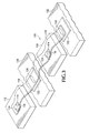
- FIGURE 3 is a top perspective view of an alternative embodiment of the ball-bump bonded ribbon-wire interconnect of the present invention.
- the ribbon-wire is translucent for the purposes of illustration.
- a preferred embodiment of the ball-bump bonded ribbon-wire interconnect of the present invention is shown and generally designated by the reference numeral 10.
- FIGURES 1 and 2 illustrate improved ball-bump bonded ribbon-wire interconnect 10 of the present invention. More particularly, the ball-bump bonded ribbon-wire interconnect 10 depicts a ribbon-wire interconnect 18 connecting an integrated circuit 12 to a substrate 20. A gold ball-bump 16 placed on the integrated circuit 12's bond pad 14, which is narrower than the ribbon-wire, to raise the surface of the bond pad 14. This enables a ribbon-bond tool to contact the ball-bump 16 to form the ball-bump bond 24 by partially flattening the ball-bump 16 as is depicted in FIGURE 2 .
- the portion of the ribbon-wire extending beyond the ball-bump 16 does not cause electrical problems such as shorts to neighboring ground pads and high parasitic capacitance because it is substantially parallel to, and spaced apart from, the surface of the integrated circuit 12.
- the ribbon-wire interconnect 18 can then be terminated at a surface bond 26 in the normal manner on the metallized surface 22 of substrate 20.
- the metallized surface 22 of substrate 20 is at least as wide as the ribbon-wire.
- the ribbon-wire is securely bonded across its full width and deformed sufficiently so it can be separated from the interconnected ribbon-wire 18 by tearing.
- the integrated circuit 12 it is preferable for the integrated circuit 12 to be at the same level or higher than the substrate 20 to avoid clearance issues with the ribbon-bonding tool.
- the upper surface of the integrated circuit 12 may also be slightly below the adjacent substrate bonding surface, as long as the bonding tool can reach the integrated circuit's surface without interference from the substrate's surface. However, this should not be viewed as limiting because equipment is available with wire cutters and advances in ribbon-bonding tool technology may eliminate this constraint in the future.
- FIGURE 3 illustrates an alternative embodiment of the improved ball-bump bonded ribbon-wire interconnect 100 of the present invention. More particularly, the alternative embodiment of the ball-bump bonded ribbon-wire interconnect 100 depicts a ribbon-wire interconnect 118 connecting multiple integrated circuits using a combination of ball-bump bonds 124 and surface bonds 126.
- the ribbon-wire interconnect 118 is connected to first integrated circuit 112 by a ball-bump bond 124, first substrate 128 by a surface bond 126, second integrated circuit 130 by a ball-bump bond 124, and second substrate 132 by a surface bond 126.
- any combination of ball-bump bonds and surface bonds can be used as the first bond or the intermediate bonds so long as the final bond is either a surface bond or is performed on a bond pad large enough to contact the full width of the bond tool-foot to terminate the ribbon-wire interconnect 118.
- this should not be viewed as limiting because advances in ribbon-bonding tool technology may eliminate this constraint in the future.
- a wire ball-bonding machine places ball-bumps on each of a workpiece's bond pads where bonds of the type disclosed are to be made (such as those that are narrower than a ribbon-wire to be employed.)
- the ball bumps have upper portions above the level of the integrated circuit that is part of the workpiece.
- the workpiece is moved to a ribbon-bonding machine or workstation.
- a bonding tool thermo-sonically welds a free end of the ribbon-wire to a first location using wedge bonding.
- the first location may be on a ball-bump or a metallized surface or bond pad that is as wide as or wider than the ribbon-wire.
- the ribbon-bonding tool then bonds the ribbon-wire to additional locations if required, which may be any combination of ball-bumps or metallized surfaces or bond pads that are as wide as or wider than the ribbon-wire, prior to terminating the ribbon-wire interconnect at a metallized surface or bond pad that is as wide as or wider than the ribbon-wire.
- the ribbon-wire could be thermo-sonically welded to all of the proximate ball bumps simultaneously.
- the present invention provides a tremendous improvement in efficiency compared to known manual methods, which have heretofore resisted automation.
- ball-bump placement by a wire ball-bonding machine ball-bump placement could be performed by alternative methods.
- ultrasonic compression bonding which applies ultrasonic energy with force over time without heating the workpiece, may be used instead of the thermo-sonic welding described.
- the ball-bump bonded ribbon-wire interconnect herein described is also suitable for use on discrete components such as diodes, transistors, and attenuators.
- wire-mesh could be used instead of the ribbon-wire.
Landscapes
- Wire Bonding (AREA)
Abstract
A ball-bump bonded ribbon-wire interconnect has a ball-bump (16) attached to an integrated circuit's bond pad (14). A ribbon-wire (18) has one end attached to the ball-bump (14) and its opposing end attached to a substrate's metallized surface (22). The ribbon-wire (18) may be wider than the ball-bump (16), and the ball-bump (16) may separate the ribbon-wire (18) from the integrated circuit's surface. The ribbon-wire may interconnect multiple integrated circuits, each of which has a ball-bump or a suitably wide metallized surface, to a substrate's metallized surface. The present invention also includes a method of electrically connecting an electronic component to a substrate.
Description
- The present invention relates to a ball-bump bonded ribbon-wire interconnect for use in connection with integrated circuits and discrete electronic components. The ball-bump bonded ribbon-wire interconnect has particular utility in connection with enabling a ribbon-wire to be bonded to an integrated circuit's bond pad that is narrower than the ribbon-wire.
- Ball-bump bonded ribbon-wire interconnects are desirable for enabling a ribbon-wire to be bonded to an integrated circuit's bond pad that is narrower than the ribbon-wire. Ribbon-wire is used when a wide signal path is desirable to limit signal loss of a high-frequency signal or avoid other adverse performance effects. Thermo-sonic wire bonding equipment exists that can place ribbon-wire interconnects, but existing techniques are limited because they require bond pads that are of equal or larger size than the ribbon-wire's width. The ribbon-wire is captured between the bond tool's foot and the pad in order to apply ultrasonic energy and force to form the bond between the ribbon-wire and the bond pad's metallization. The resulting bond establishes an electrical connection between the ribbon-wire and the bond pad's metallization.
- Therefore, the bond tool must be able to touch down on each land to form the bond, and the contact area for each bond pad must be of the same size or larger than the bond tool to properly form a bond. The problem with using the wide ribbon-wire on a narrower bond pad is that the contact areas are not the same. With a given amount of energy delivered to a smaller area when there is a smaller bond pad, adverse results can occur, including failure of the bond due to excessive energy concentration. Therefore, the combination of ultrasonic energy, force, and time must be controlled to limit the energy transferred into the bond in this circumstance.
- Furthermore, the bond pads are typically on the same surface as the integrated circuit itself or can even be recessed, which prevents the bond tool from reaching a pad without first making potentially damaging contact with the surface of the integrated circuit. Additionally, the ribbon-wire is opaque, which makes it impossible to visually locate the bond pad through the ribbon-wire to determine when the bonding tool is properly positioned to create a bond.
- The use of wire-mesh interconnects is known in the prior art. Wire mesh is used in the form of a ribbon or strip. However, hand cut pieces of gold wire-mesh are needed and have been placed manually to connect the gold wire-mesh to a bond pad having a width that is less than that of the wire-mesh. Wire-mesh enables the bond location to be viewed through the wire-mesh, which facilitates the manual alignment to a bond pad in a manner that is not possible with opaque ribbon-wire. However, this existing method requires extensive manual effort to create multiple bonds on intersections of the wire-mesh for each interconnect placed. Furthermore, when wire- mesh is bonded to a narrower bond pad, the overhanging mesh in some cases must be folded up to avoid short circuits, requiring additional manual effort.
- Therefore, a need exists for a new and improved ball-bump bonded ribbon-wire interconnect that can be used for enabling a ribbon-wire to be bonded to an integrated circuit's bond pad that is narrower than the ribbon-wire. In this regard, the various embodiments of the present invention substantially fulfill at least some of these needs. In this respect, the ball-bump bonded ribbon-wire interconnect according to the present invention substantially departs from the conventional concepts and designs of the prior art, and in doing so provides an apparatus primarily developed for the purpose of enabling a ribbon-wire to be bonded to an integrated circuit's bond pad that is narrower than the ribbon-wire.
- The present invention provides an improved ball-bump bonded ribbon-wire interconnect, and overcomes the above-mentioned disadvantages and drawbacks of the prior art. As such, the general purpose of the present invention, which will be described subsequently in greater detail, is to provide an improved ball-bump bonded ribbon-wire interconnect that has all the advantages over the prior art mentioned above.
- To attain this, the preferred embodiment of the present invention essentially comprises a ball-bump attached to an integrated circuit's bond pad. A ribbon-wire has one end attached to the ball-bump and its opposing end attached to a substrate's metallized surface. The ribbon-wire may be wider than the ball-bump, and the ball-bump may separate the ribbon-wire from the integrated circuit's surface. The ribbon-wire may interconnect multiple integrated circuits, each of which has a ball-bump or a suitably wide metallized surface, to a substrate's metallized surface. The present invention also includes a method of electrically connecting an electronic component to a substrate. There are, of course, additional features of the invention that will be described hereinafter and which will form the subject matter of the claims attached.
- There has thus been outlined, rather broadly, the more important features of the invention in order that the detailed description thereof that follows may be better understood and in order that the present contribution to the art may be better appreciated.
-
FIGURE 1 is a top view of the current embodiment of the ball-bump bonded ribbon-wire interconnect constructed in accordance with the principles of the present invention. -
FIGURE 2 is a side sectional view of the current embodiment of the ball-bump bonded ribbon-wire interconnect of the present invention. -
FIGURE 3 is a top perspective view of an alternative embodiment of the ball-bump bonded ribbon-wire interconnect of the present invention. The ribbon-wire is translucent for the purposes of illustration. - The same reference numerals refer to the same parts throughout the various figures.
- A preferred embodiment of the ball-bump bonded ribbon-wire interconnect of the present invention is shown and generally designated by the
reference numeral 10. -
FIGURES 1 and 2 illustrate improved ball-bump bonded ribbon-wire interconnect 10 of the present invention. More particularly, the ball-bump bonded ribbon-wire interconnect 10 depicts a ribbon-wire interconnect 18 connecting an integratedcircuit 12 to asubstrate 20. A gold ball-bump 16 placed on the integratedcircuit 12's bond pad 14, which is narrower than the ribbon-wire, to raise the surface of thebond pad 14. This enables a ribbon-bond tool to contact the ball-bump 16 to form the ball-bump bond 24 by partially flattening the ball-bump 16 as is depicted inFIGURE 2 . - The portion of the ribbon-wire extending beyond the ball-
bump 16 does not cause electrical problems such as shorts to neighboring ground pads and high parasitic capacitance because it is substantially parallel to, and spaced apart from, the surface of the integratedcircuit 12. The ribbon-wire interconnect 18 can then be terminated at asurface bond 26 in the normal manner on themetallized surface 22 ofsubstrate 20. Themetallized surface 22 ofsubstrate 20 is at least as wide as the ribbon-wire. At thesurface bond 26, the ribbon-wire is securely bonded across its full width and deformed sufficiently so it can be separated from the interconnected ribbon-wire 18 by tearing. In the current embodiment, it is preferable for the integratedcircuit 12 to be at the same level or higher than thesubstrate 20 to avoid clearance issues with the ribbon-bonding tool. The upper surface of the integratedcircuit 12 may also be slightly below the adjacent substrate bonding surface, as long as the bonding tool can reach the integrated circuit's surface without interference from the substrate's surface. However, this should not be viewed as limiting because equipment is available with wire cutters and advances in ribbon-bonding tool technology may eliminate this constraint in the future. -
FIGURE 3 illustrates an alternative embodiment of the improved ball-bump bonded ribbon-wire interconnect 100 of the present invention. More particularly, the alternative embodiment of the ball-bump bonded ribbon-wire interconnect 100 depicts a ribbon-wire interconnect 118 connecting multiple integrated circuits using a combination of ball-bump bonds 124 andsurface bonds 126. The ribbon-wire interconnect 118 is connected to first integratedcircuit 112 by a ball-bump bond 124,first substrate 128 by asurface bond 126, second integratedcircuit 130 by a ball-bump bond 124, andsecond substrate 132 by asurface bond 126. Any combination of ball-bump bonds and surface bonds can be used as the first bond or the intermediate bonds so long as the final bond is either a surface bond or is performed on a bond pad large enough to contact the full width of the bond tool-foot to terminate the ribbon-wire interconnect 118. However, this should not be viewed as limiting because advances in ribbon-bonding tool technology may eliminate this constraint in the future. - To connect an electronic component to a substrate by a ball-bump bonded ribbon-wire interconnect, a wire ball-bonding machine places ball-bumps on each of a workpiece's bond pads where bonds of the type disclosed are to be made (such as those that are narrower than a ribbon-wire to be employed.) The ball bumps have upper portions above the level of the integrated circuit that is part of the workpiece.
- After ball-bump placement, the workpiece is moved to a ribbon-bonding machine or workstation. There, a bonding tool thermo-sonically welds a free end of the ribbon-wire to a first location using wedge bonding. The first location may be on a ball-bump or a metallized surface or bond pad that is as wide as or wider than the ribbon-wire. The ribbon-bonding tool then bonds the ribbon-wire to additional locations if required, which may be any combination of ball-bumps or metallized surfaces or bond pads that are as wide as or wider than the ribbon-wire, prior to terminating the ribbon-wire interconnect at a metallized surface or bond pad that is as wide as or wider than the ribbon-wire. In the event a bond pad has multiple ball-bumps that are either adjacent or separated by a distance that is less than the ribbon-wire's width, the ribbon-wire could be thermo-sonically welded to all of the proximate ball bumps simultaneously. Although it is generally viewed as being inefficient to use separate passes by two different machines, the present invention provides a tremendous improvement in efficiency compared to known manual methods, which have heretofore resisted automation.
- While current embodiments of the ball-bump bonded ribbon-wire interconnect have been described in detail, it should be apparent that modifications and variations thereto are possible, all of which fall within the true spirit and scope of the invention. With respect to the above description then, it is to be realized that the optimum dimensional relationships for the parts of the invention, to include variations in size, materials, shape, form, function and manner of operation, assembly and use, are deemed readily apparent and obvious to one skilled in the art, and all equivalent relationships to those illustrated in the drawings and described in the specification are intended to be encompassed by the present invention. For example, any suitably electrically conductive and corrosion resistant material could be used instead of the gold ball-bumps. Furthermore, although ball-bump placement by a wire ball-bonding machine has been described, ball-bump placement could be performed by alternative methods. In addition, ultrasonic compression bonding, which applies ultrasonic energy with force over time without heating the workpiece, may be used instead of the thermo-sonic welding described. And although enabling a ribbon-wire to be bonded to an integrated circuit's bond pad that is narrower than the ribbon-wire has been described, it should be appreciated that the ball-bump bonded ribbon-wire interconnect herein described is also suitable for use on discrete components such as diodes, transistors, and attenuators. Furthermore, wire-mesh could be used instead of the ribbon-wire.
- Therefore, the foregoing is considered as illustrative only of the principles of the invention. Further, since numerous modifications and changes will readily occur to those skilled in the art, it is not desired to limit the invention to the exact construction and operation shown and described, and accordingly, all suitable modifications and equivalents may be resorted to, falling within the scope of the invention.
Claims (15)
- A ball-bump bonded ribbon-wire interconnect comprising:a first electronic component connected to a substrate having a metallized surface portion;the first electronic component having an upper surface including a bond pad;a ball-bump having a bump width, the ball-bump being attached to the first electronic component's bond pad;a ribbon-wire having a ribbon width;the ribbon-wire having opposed ends;the ribbon-wire having a middle;one of the opposed ends being attached to the first electronic component's ball-bump;a second electronic component connected to the substrate having a metallized surface portion;the second electronic component having an upper surface including a bond pad;a ball-bump having a bump width, the ball-bump being attached to the second electronic component's bond pad;the middle of the ribbon-wire being attached to the second electronic component's ball-bump; andanother of the opposed ends of the ribbon-wire being attached to the metallized surface portion.
- The ball-bump bonded ribbon-wire interconnect as defined in claim 1, wherein the ball-bumps have an upper portion extending above the electronic components' upper surfaces.
- The ball-bump bonded ribbon-wire interconnect as defined in claim 1, wherein the ribbon width is wider than the bump width.
- The ball-bump bonded ribbon-wire interconnect as defined in claim 1, wherein the ball-bumps extend above the bond pads.
- The ball-bump bonded ribbon-wire interconnect as defined in claim 1, wherein the ribbon-wire is separated from the electronic components' upper surfaces by the ball-bumps.
- The ball-bump bonded ribbon-wire interconnect as defined in claim 1, wherein the ribbon-wire is thermo-sonically welded to the ball-bumps.
- The ball-bump bonded ribbon-wire interconnect as defined in claim 1, wherein the ribbon-wire is thermo-sonically welded to the metallized surface.
- A method of electrically connecting an electronic component to a substrate comprising the steps:providing a ribbon-wire having a free end and a second portion, a substrate having a metallized surface portion; and a component connected to the substrate and having an upper surface including a bond pad;attaching a ball-bump to the bond pad;attaching the free end of the ribbon-wire to the ball-bump; andattaching a second portion of the ribbon-wire to the metallized surface portion.
- The method of electrically connecting an electronic component to a substrate as defined in claim 8, wherein the ball-bump is attached to the bond pad by a wire ball-bonding facility.
- The method of electrically connecting an electronic component to a substrate as defined in claim 8, wherein the ribbon-wire is attached to the ball-bump and to the metallized surface by a ribbon-wire bonding facility.
- The method of electrically connecting and electronic component to a substrate as defined in claim 10, further comprising the step of separating the ribbon-wire adjacent to the second portion using the ribbon-wire bonding facility from the second portion.
- The method of electrically connecting an electronic component to a substrate as defined in claim 8, wherein the ribbon-wire is wider than the ball-bump.
- The method of electrically connecting an electronic component to a substrate as defined in claim 8, wherein the ribbon-wire is thermo-sonically welded to the ball-bump and to the metallized surface.
- A ball-bump bonded ribbon-wire interconnect comprising:a first electronic component connected to a substrate;the electronic component having an upper surface including a bond pad;the substrate including a second electrical contact other than the bond pad;a ball-bump having a bump width;the ball-bump being attached to the bond pad;a ribbon-wire having a ribbon width;a first portion of the ribbon-wire being attached to the ball-bump; anda second portion of the ribbon-wire being attached to the second electrical contact.
- The ball-bump bonded ribbon-wire interconnect as defined in claim 1, wherein the second electrical contact is one of a metallized contact on a surface of the substrate and a bond pad of a second electronic component attached to the substrate.
Applications Claiming Priority (1)
| Application Number | Priority Date | Filing Date | Title |
|---|---|---|---|
| US12/122,213 US7977804B2 (en) | 2008-05-16 | 2008-05-16 | Ball-bump bonded ribbon-wire interconnect |
Publications (1)
| Publication Number | Publication Date |
|---|---|
| EP2120259A1 true EP2120259A1 (en) | 2009-11-18 |
Family
ID=40887084
Family Applications (1)
| Application Number | Title | Priority Date | Filing Date |
|---|---|---|---|
| EP09251320A Withdrawn EP2120259A1 (en) | 2008-05-16 | 2009-05-14 | Ball-bump bonded ribbon-wire interconnect |
Country Status (4)
| Country | Link |
|---|---|
| US (1) | US7977804B2 (en) |
| EP (1) | EP2120259A1 (en) |
| JP (1) | JP5971886B2 (en) |
| CN (1) | CN101582398B (en) |
Cited By (1)
| Publication number | Priority date | Publication date | Assignee | Title |
|---|---|---|---|---|
| EP2743973A3 (en) * | 2012-12-11 | 2014-12-03 | Robert Bosch Gmbh | Method for contacting a semiconductor element by welding a contact element to a sintered layer on the semiconductor element and semiconductor component with increased stability against thermomechanical influence |
Families Citing this family (2)
| Publication number | Priority date | Publication date | Assignee | Title |
|---|---|---|---|---|
| US10431545B2 (en) * | 2017-06-29 | 2019-10-01 | Intel IP Corporation | Cross-connected multi-chip modules coupled by silicon bent-bridge interconnects and methods of assembling same |
| DE102022210631A1 (en) | 2022-10-07 | 2024-04-18 | Volkswagen Aktiengesellschaft | Component arrangement for power electronics and method for providing a component arrangement for power electronics |
Citations (7)
| Publication number | Priority date | Publication date | Assignee | Title |
|---|---|---|---|---|
| JP2001237263A (en) * | 2000-02-24 | 2001-08-31 | Hitachi Ltd | High frequency circuit device and method of manufacturing the same |
| US6500760B1 (en) * | 2001-08-02 | 2002-12-31 | Sandia Corporation | Gold-based electrical interconnections for microelectronic devices |
| JP2003303845A (en) * | 2002-04-10 | 2003-10-24 | Fuji Electric Co Ltd | Semiconductor device and wire bonding method |
| US20050200015A1 (en) * | 2004-03-10 | 2005-09-15 | Nec Electronics Corporation | Semiconductor device and method for manufacturing the same |
| US20050200009A1 (en) * | 2004-03-11 | 2005-09-15 | In-Ku Kang | Method and apparatus for bonding a wire |
| US20060012016A1 (en) * | 2002-05-22 | 2006-01-19 | Bernd Betz | High-frequency power semiconductor module with a hollow housing and method for the production thereof |
| WO2006018671A1 (en) * | 2004-08-19 | 2006-02-23 | Infineon Technologies Ag | Mixed wire semiconductor lead frame package |
Family Cites Families (5)
| Publication number | Priority date | Publication date | Assignee | Title |
|---|---|---|---|---|
| JPS61116850A (en) * | 1984-11-12 | 1986-06-04 | Mitsubishi Electric Corp | Semiconductor device |
| US5976964A (en) * | 1997-04-22 | 1999-11-02 | Micron Technology, Inc. | Method of improving interconnect of semiconductor device by utilizing a flattened ball bond |
| JP3865055B2 (en) * | 2001-12-28 | 2007-01-10 | セイコーエプソン株式会社 | Manufacturing method of semiconductor device |
| JP4265394B2 (en) * | 2003-12-17 | 2009-05-20 | 株式会社日立製作所 | Power converter |
| JP4722757B2 (en) * | 2006-04-19 | 2011-07-13 | ルネサスエレクトロニクス株式会社 | Manufacturing method of semiconductor device |
-
2008
- 2008-05-16 US US12/122,213 patent/US7977804B2/en not_active Expired - Fee Related
-
2009
- 2009-05-14 EP EP09251320A patent/EP2120259A1/en not_active Withdrawn
- 2009-05-15 CN CN2009101390935A patent/CN101582398B/en not_active Expired - Fee Related
- 2009-05-18 JP JP2009120357A patent/JP5971886B2/en not_active Expired - Fee Related
Patent Citations (7)
| Publication number | Priority date | Publication date | Assignee | Title |
|---|---|---|---|---|
| JP2001237263A (en) * | 2000-02-24 | 2001-08-31 | Hitachi Ltd | High frequency circuit device and method of manufacturing the same |
| US6500760B1 (en) * | 2001-08-02 | 2002-12-31 | Sandia Corporation | Gold-based electrical interconnections for microelectronic devices |
| JP2003303845A (en) * | 2002-04-10 | 2003-10-24 | Fuji Electric Co Ltd | Semiconductor device and wire bonding method |
| US20060012016A1 (en) * | 2002-05-22 | 2006-01-19 | Bernd Betz | High-frequency power semiconductor module with a hollow housing and method for the production thereof |
| US20050200015A1 (en) * | 2004-03-10 | 2005-09-15 | Nec Electronics Corporation | Semiconductor device and method for manufacturing the same |
| US20050200009A1 (en) * | 2004-03-11 | 2005-09-15 | In-Ku Kang | Method and apparatus for bonding a wire |
| WO2006018671A1 (en) * | 2004-08-19 | 2006-02-23 | Infineon Technologies Ag | Mixed wire semiconductor lead frame package |
Non-Patent Citations (1)
| Title |
|---|
| GEORGE G. HARMAN: "Wire Bonding in Microelectronics Materials, Processes, Reliability, and Yield 2ed.", 1997, MCGRAW-HILL, UNITED STATES OF AMERICA, ISBN: 0-07-032619-3, XP002539702 * |
Cited By (1)
| Publication number | Priority date | Publication date | Assignee | Title |
|---|---|---|---|---|
| EP2743973A3 (en) * | 2012-12-11 | 2014-12-03 | Robert Bosch Gmbh | Method for contacting a semiconductor element by welding a contact element to a sintered layer on the semiconductor element and semiconductor component with increased stability against thermomechanical influence |
Also Published As
| Publication number | Publication date |
|---|---|
| US20090283920A1 (en) | 2009-11-19 |
| JP2009278116A (en) | 2009-11-26 |
| CN101582398A (en) | 2009-11-18 |
| JP5971886B2 (en) | 2016-08-17 |
| US7977804B2 (en) | 2011-07-12 |
| CN101582398B (en) | 2013-06-19 |
Similar Documents
| Publication | Publication Date | Title |
|---|---|---|
| CN100361285C (en) | Wire bonding method and semiconductor device | |
| US6192578B1 (en) | Method for electrically coupling bond pads of a microelectronic device | |
| CN104885208B (en) | Manufacturing method of semiconductor device | |
| JP3115155B2 (en) | Semiconductor device and manufacturing method thereof | |
| US12255109B2 (en) | Methods of detecting bonding between a bonding wire and a bonding location on a wire bonding machine | |
| WO2006053277A2 (en) | Wire bond interconnection | |
| US7977804B2 (en) | Ball-bump bonded ribbon-wire interconnect | |
| TWI511209B (en) | Conductive bump, wire loop and forming method thereof | |
| US20070029367A1 (en) | Semiconductor device | |
| KR101496997B1 (en) | Wire bonding structure and method that eliminates special wire bondable finish and reduces bonding pitch on substrates | |
| US20040164127A1 (en) | Wire bonding method | |
| US6156626A (en) | Electromigration bonding process and system | |
| KR100808613B1 (en) | Semiconductor device and manufacturing method for the same | |
| CN102017112B (en) | Electric pressure welding connection device | |
| TWI395301B (en) | Folding frame carrier using metal oxide semiconductor field effect transistor ball grid array packaging technology | |
| JP4547523B2 (en) | Chip component assembly and manufacturing method thereof | |
| JP3620213B2 (en) | Bump forming device | |
| CN101651106B (en) | Manufacturing method of stacked chip package structure | |
| US20050110139A1 (en) | Customized microelectronic device and method for making customized electrical interconnections | |
| JP3588641B2 (en) | Semiconductor device joining structure and joining method | |
| KR20230132817A (en) | Ball junction impedance matching | |
| JP3855532B2 (en) | Connection method between IC chip and circuit board | |
| EP0844664A2 (en) | A bond pad for an integrated circuit | |
| CN100495695C (en) | array circuit substrate | |
| US5513429A (en) | Method of reworking bonded lead wires |
Legal Events
| Date | Code | Title | Description |
|---|---|---|---|
| PUAI | Public reference made under article 153(3) epc to a published international application that has entered the european phase |
Free format text: ORIGINAL CODE: 0009012 |
|
| AK | Designated contracting states |
Kind code of ref document: A1 Designated state(s): AT BE BG CH CY CZ DE DK EE ES FI FR GB GR HR HU IE IS IT LI LT LU LV MC MK MT NL NO PL PT RO SE SI SK TR |
|
| 17P | Request for examination filed |
Effective date: 20100505 |
|
| 17Q | First examination report despatched |
Effective date: 20100610 |
|
| RAP1 | Party data changed (applicant data changed or rights of an application transferred) |
Owner name: TEKTRONIX, INC. |
|
| STAA | Information on the status of an ep patent application or granted ep patent |
Free format text: STATUS: THE APPLICATION IS DEEMED TO BE WITHDRAWN |
|
| 18D | Application deemed to be withdrawn |
Effective date: 20180609 |