EP2115872B1 - Common-mode insensitive sampler - Google Patents
Common-mode insensitive sampler Download PDFInfo
- Publication number
- EP2115872B1 EP2115872B1 EP08713358.3A EP08713358A EP2115872B1 EP 2115872 B1 EP2115872 B1 EP 2115872B1 EP 08713358 A EP08713358 A EP 08713358A EP 2115872 B1 EP2115872 B1 EP 2115872B1
- Authority
- EP
- European Patent Office
- Prior art keywords
- common
- mode
- voltage
- input
- sampler
- Prior art date
- Legal status (The legal status is an assumption and is not a legal conclusion. Google has not performed a legal analysis and makes no representation as to the accuracy of the status listed.)
- Not-in-force
Links
- 239000003990 capacitor Substances 0.000 claims description 32
- 238000005070 sampling Methods 0.000 claims description 31
- 238000012937 correction Methods 0.000 claims description 6
- 238000000034 method Methods 0.000 claims description 4
- 238000007599 discharging Methods 0.000 claims 4
- 238000010586 diagram Methods 0.000 description 10
- 238000013459 approach Methods 0.000 description 4
- 238000012546 transfer Methods 0.000 description 3
- 238000006243 chemical reaction Methods 0.000 description 2
- 230000015556 catabolic process Effects 0.000 description 1
- 238000006731 degradation reaction Methods 0.000 description 1
- 238000013461 design Methods 0.000 description 1
Images




Classifications
-
- H—ELECTRICITY
- H03—ELECTRONIC CIRCUITRY
- H03M—CODING; DECODING; CODE CONVERSION IN GENERAL
- H03M1/00—Analogue/digital conversion; Digital/analogue conversion
- H03M1/12—Analogue/digital converters
- H03M1/34—Analogue value compared with reference values
-
- H—ELECTRICITY
- H03—ELECTRONIC CIRCUITRY
- H03M—CODING; DECODING; CODE CONVERSION IN GENERAL
- H03M1/00—Analogue/digital conversion; Digital/analogue conversion
- H03M1/06—Continuously compensating for, or preventing, undesired influence of physical parameters
- H03M1/0617—Continuously compensating for, or preventing, undesired influence of physical parameters characterised by the use of methods or means not specific to a particular type of detrimental influence
- H03M1/0634—Continuously compensating for, or preventing, undesired influence of physical parameters characterised by the use of methods or means not specific to a particular type of detrimental influence by averaging out the errors, e.g. using sliding scale
- H03M1/0636—Continuously compensating for, or preventing, undesired influence of physical parameters characterised by the use of methods or means not specific to a particular type of detrimental influence by averaging out the errors, e.g. using sliding scale in the amplitude domain
-
- H—ELECTRICITY
- H03—ELECTRONIC CIRCUITRY
- H03M—CODING; DECODING; CODE CONVERSION IN GENERAL
- H03M1/00—Analogue/digital conversion; Digital/analogue conversion
- H03M1/12—Analogue/digital converters
- H03M1/124—Sampling or signal conditioning arrangements specially adapted for A/D converters
- H03M1/1245—Details of sampling arrangements or methods
Definitions
- FIG. 1 While a single-ended sampler/converter can be made from the circuits shown in Figure 1 , more commonly, a pair of single-end samplers/converters are mated together to form a differential configuration, as shown in Figure 2 .
- FIG. 3 and 4 Illustration of the sampler/converter input circuitry is illustrated in Figures 3 and 4 , showing the two primary clock phases, track and hold). The circuits are mirrored about the horizontal center-line, creating m (minus) and p (plus) halves of the sampler/converter.
- the sampler converts input voltage to charge stored on the sampling capacitors, so any input common-mode-voltage variation will result in a common-mode charge variation on the two sampling capacitors. Downstream circuitry must then be able to accommodate this common-mode variation without a loss in performance.
- a second approach to driving the converter inputs is to precede the converter with an active differential amplifier, as mentioned above.
- This differential amplifier can provide some degree of common-mode rejection, like the transformer. But again, real-life amplifiers aren't perfect, and they too leave a residual common-mode voltage variation for the sampler/converter to deal with. Additionally, these active amplifiers add distortion and noise, often exceeding that of the sampler/converter itself.
- Document EP1594272 A2 discloses an input sampling circuit which samples the input in a first phase and connects the common mode to discharge the sampling circuit in a second phase.
- Figure 5 provides the relationship between input differential and common-mode voltage, Vdiff and Vcm, respectively, and output differential and common-mode charge, Qdiff and Qcm.
- the differential-mode output charge is simply the product of the differential-mode input voltage and the sampling capacitance, as desired.
- the common-mode output charge is a function of the input common-mode voltage, the precharge (Vpch) and discharge (Vdch) voltages, a downstream voltage (Vfdss), the sampling capacitance, and any bottom-plate capacitance (Cbp).
- the proposed common-mode-insensitive (Vcm-tracking) sampler of Figure 7 which is an embodiment of the invention, theoretically has infinite common-mode rejection, as the common-mode output charge is not a function of the input common-mode voltage.
- an ideal voltage source is needed to maintain Vdch at a constant voltage-drop below Vcmi. In practice, this voltage source will have non-zero output impedance, and also finite operating range. Additionally, if the common-mode input voltage is varying with time, when the input signal is sampled, Vcmi also needs to be sampled at the same time.
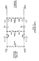
- FIG. 8 shows a practical implementation of the Vcm-tracking sampler.
- An additional sample-and-hold circuit (capacitor Ci and additional switch Kbp) is added to the common-mode sensing path, and followed by a buffer amplifier Ab having low output impedance. While the analog input signals Vinp, Vinm and common-mode signal Vcmi are being sampled onto their respective capacitors (Cs and Ci, respectively), simultaneously; a large common-mode-correction capacitor Ccmc is being charged up to a fixed reference voltage, Vcmc_samp. During the charge transfer phase, the Ccmc is connected in series between the output of the buffer-amplifier Ab and vdch, resulting in a fixed offset between Vcmi_s and Vdch, as desired.
- Ccmc can be made relatively large. Since this capacitor is in a path common to both sampler halves, no differential KTC noise is added to the charge outputs. As the value of Ccmc increases, the required Vcmc_samp drops, eventually approaching Vcm. Note that in addition to providing rejection of common-mode input variations, Vcmc_samp can be used as a means to adjust the common-mode output charge of the sampler.
- the circuit first enters a sampling state to obtain samples of analog input signals Vinp, Vinm and common-mode signal Vcmi.
- switches clocked by Kbp and Ktp are closed, while switches clocked by Kct are opened, enabling capacitors Cs to sample respective input signals Vinp and Vinm.
- the switch connecting Vcmi to Ci is closed, enabling capacitor Ci to sample the common mode voltage Vcmi.
- the common mode voltage Vcmi may be sampled simultaneously with the sampling of the input signals Vinp and Vinm.
- Ccmc is charged up to Vcmc_samp by a pair of switches controlled by Kbp and Ktp, respectively.
- the sampling circuit may enter a transfer state to transfer the sampled charges via charge outputs Vfdp, Vfdm.
- Switches controlled by Kbp and Ktp are opened, and switches controlled by Kct are closed.
- the buffered-version of the sampled common-mode voltage, Vcmi_s drives one side of the correction capacitor Ccmc, forcing the other node connected to this capacitor, Vdch, down to Vcmi-Vcmc_samp. This, in turn, drives the charge out of the sampling capacitors into the downstream circuitry.
- the sampling circuit provides sampled differential output charges at charge outputs Vfdp, Vfdm having a constant common-mode charge Qcm that is independent of the common mode input voltage Vcmi.
- Vdch 0.
- Vdch 0.
- Vdch 0.
- Vdch in the legacy sampler of Fig. 6 is constant, resulting in variations in output common-mode charge.
- Vdch moves up and down by the same amount to match, maintaining the output common-mode charge (at Vfdp and Vfdm) at a constant value.
- the measured performance of the Vcm-tracking sampler of Figure 8 is shown in the dc sweeps of Figure 9 .
- the output common-mode charge is recorded.
- Two sets of three curves are shown: the legacy-sampler and the vcm-tracking sampler performance, at each of three temperatures, -40C, +40C, and 120C.
- the legacy sampler responds directly to changes in Vcm, for this particular sampler, with a slope of 1.6fC/mV.
- the Vcm-tracking sampler provides about 16x reduction in common-mode charge variation to the downstream circuitry, with a slope of 0.1 fC/mV.
- Embodiments of the present invention may provide common-mode variation rejection for time-varying input signals.
- Figure 10 illustrates the response of the samplers of Fig. 6 and Fig. 8 to a 10% mismatch in vinm and vinp, at three different input frequencies (10, 260, and 510 MHz), and the same three temperatures. This mismatch produces a large, time-varying input common-mode variation.
- the legacy-sampler Fig. 6
- the Vcm-tracking sampler ( Fig. 8 ) substantially rejects these dynamic input common-mode signals.
- the 10MHz cases are very similar to the dc case shown in Fig. 9 , providing a large amount common-mode rejection. As the input frequency is raised, the common-mode rejection gradually degrades, but even at 510 MHz input, the Vcm-tracking sampler still provides about a 2.5 to 3x reduction in output common-mode charge fluctuation.
- the alternative common-mode sense circuit of Figure 11 can be employed. This circuit uses a pair of switched-capacitors to sense the common-mode input voltage, and places the buffer amplifier directly on vdch. For applications where vdch needs to be near or below ground, this topology also requires a negative supply rail or charge-pump (not shown) to sink the sampling charge into, as the buffer maintains vdch near zero volts. Note that the Ccmc capacitor in Figure 8 provides a similar charge-pump function along with the offset function already discussed.
- Embodiments of the present invention may also be applied to op-amp-based converters, as shown for example in Fig. 1(a) .
- Such converters typically achieve common-mode rejection by way of differential amplifiers.
- a common-mode tracking sampler as described above may be implemented in such a converter to provide common-mode rejection prior to the differential amplifiers.
- the sampler of Fig. 7 may be configured in a pipeline preceding a differential amplifier (not shown), the differential amplifier receiving inputs Vfdp and Vfdm and providing a corresponding voltage differential.
Landscapes
- Engineering & Computer Science (AREA)
- Theoretical Computer Science (AREA)
- Amplifiers (AREA)
- Analogue/Digital Conversion (AREA)
Description
- This application claims the benefit of
U.S. Provisional Application No. 60/898,216, filed on January 30, 2007 - In many (high-speed) analog-to-digital converters (ADCs), the analog input-signal is sampled onto input sampling-capacitors prior to conversion. Any intervening circuitry between the analog input and the sampling capacitors can be a source of degradation, adding distortion and/or noise. Therefore, to achieve the highest possible spurious-free-dynamic-Range (SFDR) and highest Signal-to-Noise-Ratio (SNR), many high-performance samplers and ADCs leave out active front-end differential amplifiers, resulting in topologies similar to those shown in
Figure 1. Figure 1a shows a conventional op-amp based design, andFigure 1b shows Kenet's Common-gate-charge-pipeline sampling front-end (covered by other patents). Note how both approaches employ the same switch-capacitor network attached to the analog inputs, with similarly timed clocking. The rest of this description will be based on results obtained with Kenet's Common-gate-charge-pipeline, but the unique features of the disclosed sampler could be applied equally well to the conventional approach. - While a single-ended sampler/converter can be made from the circuits shown in
Figure 1 , more commonly, a pair of single-end samplers/converters are mated together to form a differential configuration, as shown inFigure 2 . (Operation of the sampler/converter input circuitry is illustrated inFigures 3 and4 , showing the two primary clock phases, track and hold). The circuits are mirrored about the horizontal center-line, creating m (minus) and p (plus) halves of the sampler/converter. Ideally, a differential signal, vdiff, is applied to the vinp and vinm inputs, centered about some common-mode value, Vcm, i.e., Vinp = Vcm + vdiff/2, Vinm = Vcm - vdiff/2. - In practice, most analog inputs, even those intended to be fully differential, have some residual common-mode voltage variation as the differential-signal swings through its range. For example, the inputs of high-speed converters are often driven from transformer-based baluns that perform unbalanced (single-ended) to balanced (differential) conversion. These baluns are not perfect, resulting in a common-mode component at their outputs. Another way to say this is that if vinp and vinm do not have equal amplitudes and exactly 180° relative-phase, a residual time-varying common-mode component will appear at the sampler/converter inputs. The sampler converts input voltage to charge stored on the sampling capacitors, so any input common-mode-voltage variation will result in a common-mode charge variation on the two sampling capacitors. Downstream circuitry must then be able to accommodate this common-mode variation without a loss in performance.
- A second approach to driving the converter inputs is to precede the converter with an active differential amplifier, as mentioned above. This differential amplifier can provide some degree of common-mode rejection, like the transformer. But again, real-life amplifiers aren't perfect, and they too leave a residual common-mode voltage variation for the sampler/converter to deal with. Additionally, these active amplifiers add distortion and noise, often exceeding that of the sampler/converter itself.
- Document
EP1594272 A2 discloses an input sampling circuit which samples the input in a first phase and connects the common mode to discharge the sampling circuit in a second phase. - What is needed is an approach to rejecting input common-mode voltage variations without the use of a differential amplifier in the signal path, and without any added distortion or noise. Said problem is solved by a device or method defined according to claims 1 and 11 respectively.
- The foregoing will be apparent from the following more particular description of example embodiments of the invention, as illustrated in the accompanying drawings in which like reference characters refer to the same parts throughout the different views. The drawings are not necessarily to scale, emphasis instead being placed upon illustrating embodiments of the present invention.
-
FIG. 1a is a schematic diagram of a conventional op-amp based converter. -
FIG. 1b is a schematic diagram of a charge pipeline converter. -
FIG. 2 is a schematic diagram of a charge sampler in a differential configuration. -
FIG. 3 is a schematic diagram of the sampler ofFig. 2 during a sampling phase. -
FIG. 4 is a schematic diagram of the sampler ofFig. 2 during a discharge phase. -
FIG. 5 is a schematic diagram of the sampler ofFig. 2 illustrating the relation of charge output to voltage input. -
FIG. 6 is a schematic diagram of the sampler ofFig. 2 illustrating the relation of common-mode charge output to common mode voltage input. -
FIG. 7 is a schematic diagram of a common-mode insensitive sampler employing a voltage source. -
FIG. 8 is a schematic diagram of a common-mode insensitive sampler. -
FIG. 9 is a plot of common-mode charge in relation to common-mode voltage for conventional and common-mode insensitive samplers. -
FIG. 10 is a plot of common-mode charge in relation to common-mode, time-varying voltage for conventional and common-mode insensitive samplers. -
FIG. 11 is a schematic diagram of a switched-capacitor common-mode insensitive sampler. -
Figure 5 provides the relationship between input differential and common-mode voltage, Vdiff and Vcm, respectively, and output differential and common-mode charge, Qdiff and Qcm. The differential-mode output charge is simply the product of the differential-mode input voltage and the sampling capacitance, as desired. On the other hand, the common-mode output charge is a function of the input common-mode voltage, the precharge (Vpch) and discharge (Vdch) voltages, a downstream voltage (Vfdss), the sampling capacitance, and any bottom-plate capacitance (Cbp). - In the conventional (or "legacy") sampler of
Figure 6 , Vdch and Vpch are grounded, resulting in a common-mode output charge (Qcm) that is equal to a constant plus a term that is the product of the input common-mode voltage and the sampling capacitance. In other words, any common-mode input variations pass directly through this sampler with the same gain as the desired input signal, so this topology provides absolutely no common-mode rejection. - In contrast, the proposed common-mode-insensitive (Vcm-tracking) sampler of
Figure 7 , which is an embodiment of the invention, theoretically has infinite common-mode rejection, as the common-mode output charge is not a function of the input common-mode voltage. To achieve this, an ideal voltage source is needed to maintain Vdch at a constant voltage-drop below Vcmi. In practice, this voltage source will have non-zero output impedance, and also finite operating range. Additionally, if the common-mode input voltage is varying with time, when the input signal is sampled, Vcmi also needs to be sampled at the same time. -
Figure 8 shows a practical implementation of the Vcm-tracking sampler. An additional sample-and-hold circuit (capacitor Ci and additional switch Kbp) is added to the common-mode sensing path, and followed by a buffer amplifier Ab having low output impedance. While the analog input signals Vinp, Vinm and common-mode signal Vcmi are being sampled onto their respective capacitors (Cs and Ci, respectively), simultaneously; a large common-mode-correction capacitor Ccmc is being charged up to a fixed reference voltage, Vcmc_samp. During the charge transfer phase, the Ccmc is connected in series between the output of the buffer-amplifier Ab and vdch, resulting in a fixed offset between Vcmi_s and Vdch, as desired. To minimize the capacitive division effect between Ccmc and the sampling capacitors, Ccmc can be made relatively large. Since this capacitor is in a path common to both sampler halves, no differential KTC noise is added to the charge outputs. As the value of Ccmc increases, the required Vcmc_samp drops, eventually approaching Vcm. Note that in addition to providing rejection of common-mode input variations, Vcmc_samp can be used as a means to adjust the common-mode output charge of the sampler. - Returning to the operation of the sampler circuit in
Fig. 8 , the circuit first enters a sampling state to obtain samples of analog input signals Vinp, Vinm and common-mode signal Vcmi. In this sampling state, switches clocked by Kbp and Ktp are closed, while switches clocked by Kct are opened, enabling capacitors Cs to sample respective input signals Vinp and Vinm. Concurrently, the switch connecting Vcmi to Ci is closed, enabling capacitor Ci to sample the common mode voltage Vcmi. As a result, the common mode voltage Vcmi may be sampled simultaneously with the sampling of the input signals Vinp and Vinm. Simultaneously, Ccmc is charged up to Vcmc_samp by a pair of switches controlled by Kbp and Ktp, respectively. - Upon completing sampling of the signals Vinp, Vinm and Vcmi, the sampling circuit may enter a transfer state to transfer the sampled charges via charge outputs Vfdp, Vfdm. Switches controlled by Kbp and Ktp are opened, and switches controlled by Kct are closed. As a result, the buffered-version of the sampled common-mode voltage, Vcmi_s, drives one side of the correction capacitor Ccmc, forcing the other node connected to this capacitor, Vdch, down to Vcmi-Vcmc_samp. This, in turn, drives the charge out of the sampling capacitors into the downstream circuitry. For large Ccmc (Ccmc»Cc), there is minimal capaciteive charge division, so Vdch is held at a constant voltage drop below the common mode input Vcmi, thereby tracking any common-mode variation of sampled charges at capacitors Cs (due to input common-mode changes at Vinp and Vinm). Thus, the sampling circuit provides sampled differential output charges at charge outputs Vfdp, Vfdm having a constant common-mode charge Qcm that is independent of the common mode input voltage Vcmi.
- Note that in the legacy sampler of
Fig. 6 , Vdch = 0. In the Vcm-tracking sampler ofFigure 8 , Vdch is also driven to near 0V for large Ccmc and Vcmc_samp set equal to Vcm. As the input common-mode voltage varies, Vdch in the legacy sampler ofFig. 6 is constant, resulting in variations in output common-mode charge. In contrast, in the Vcm-tracking sampler ofFig. 8 , as the input common-mode voltage varies (at Vinp and Vinm), Vdch moves up and down by the same amount to match, maintaining the output common-mode charge (at Vfdp and Vfdm) at a constant value. - The measured performance of the Vcm-tracking sampler of
Figure 8 is shown in the dc sweeps ofFigure 9 . In these sweeps, the input common-mode voltage is swept around its nominal value, while the input differential-mode voltage is set to zero, i.e., vinm = vinp = Vcm. The output common-mode charge is recorded. Two sets of three curves are shown: the legacy-sampler and the vcm-tracking sampler performance, at each of three temperatures, -40C, +40C, and 120C. As expected, the legacy sampler responds directly to changes in Vcm, for this particular sampler, with a slope of 1.6fC/mV. In contrast, the Vcm-tracking sampler provides about 16x reduction in common-mode charge variation to the downstream circuitry, with a slope of 0.1 fC/mV. - Embodiments of the present invention may provide common-mode variation rejection for time-varying input signals.
Figure 10 illustrates the response of the samplers ofFig. 6 andFig. 8 to a 10% mismatch in vinm and vinp, at three different input frequencies (10, 260, and 510 MHz), and the same three temperatures. This mismatch produces a large, time-varying input common-mode variation. For all cases, the legacy-sampler (Fig. 6 ) passes this common-mode voltage fluctuation right through the charge outputs, resulting in unacceptably large common-mode charge variations. - In contrast, the Vcm-tracking sampler (
Fig. 8 ) substantially rejects these dynamic input common-mode signals. The 10MHz cases are very similar to the dc case shown inFig. 9 , providing a large amount common-mode rejection. As the input frequency is raised, the common-mode rejection gradually degrades, but even at 510 MHz input, the Vcm-tracking sampler still provides about a 2.5 to 3x reduction in output common-mode charge fluctuation. - While most high-speed converters require a relatively low source impedance to achieve high bandwidths, some applications cannot tolerate resistor loads coupled directly to the sampler inputs. For those or other applications, the alternative common-mode sense circuit of
Figure 11 can be employed. This circuit uses a pair of switched-capacitors to sense the common-mode input voltage, and places the buffer amplifier directly on vdch. For applications where vdch needs to be near or below ground, this topology also requires a negative supply rail or charge-pump (not shown) to sink the sampling charge into, as the buffer maintains vdch near zero volts. Note that the Ccmc capacitor inFigure 8 provides a similar charge-pump function along with the offset function already discussed. - Embodiments of the present invention may also be applied to op-amp-based converters, as shown for example in
Fig. 1(a) . Such converters typically achieve common-mode rejection by way of differential amplifiers. However, a common-mode tracking sampler as described above may be implemented in such a converter to provide common-mode rejection prior to the differential amplifiers. For example, the sampler ofFig. 7 may be configured in a pipeline preceding a differential amplifier (not shown), the differential amplifier receiving inputs Vfdp and Vfdm and providing a corresponding voltage differential. - While this invention has been particularly shown and described with references to example embodiments thereof, it will be understood by those skilled in the art that various changes in form and details may be made therein without departing from the scope of the invention encompassed by the appended claims.
Claims (13)
- An apparatus for rejecting common-mode input voltage variations in a differential sampler comprising:a first sampler (ktp, kbp, kct, Cs), configured to sample a first voltage (vinp) of a differential input signal, at a given time, the first voltage having a first common mode component;a second sampler (ktp, kbp, kct, Cs), configured to sample a second voltage (vinm) of the differential input signal, at the given time, the second voltage having a second common mode component;a circuit configured to sense common-mode variations in the first and second voltages, the circuit detecting such common-mode variations as a corresponding common mode voltage (Vcmi);a third sampler (kbp, Ci), configured to sample the common mode voltage (Vcmi), at the given time;a discharge path connected to the first and second sampler and also connected to a common discharge node (Vdch), to provide a common path for discharging sampled charge for each of the first and second samplers;characterized by:
a fixed voltage source (Ccmc), configured to maintain the discharge node (Vdch), at a substantially constant voltage difference with respect to the common mode voltage (Vcmi). - An apparatus as in claim 1, wherein the voltage source includes a common-mode correction capacitor (Ccmc), which is connected in series between the input node (Vcmi) of the common mode sensing path and the discharge node (Vdch).
- An apparatus as in claim 2, wherein the first sampler includes a plurality of input sampling capacitors (Cs), the common-mode correction capacitor (Ccmc), having a capacitance substantially larger than capacitance of each of the input sampling capacitors (Cs).
- An apparatus as in claim 3, wherein the input sampling capacitors (Cs) are connected to the discharge node (Vdch) and discharge charge via the discharge node (Vdch),
- An apparatus as in claim 3, further comprising charge outputs connected to the input sampling capacitors (Cs), respectively, for providing an output charge corresponding to the differential input voltage (Vdiff) sampled by the first sampler.
- An apparatus as in claim 5, wherein the output charge is a plurality of charges having an output common-mode charge (Qcm) that remains substantially constant relative to variation of the common mode voltage (Vcmi).
- An apparatus as in claim 5, wherein the charge outputs are coupled to a differential amplifier.
- An apparatus as in claim 1 wherein the circuit for sensing the common-mode input variations comprises a pair of resistors connected between the input sampling capacitors (Cs),
- An apparatus as in claim 8 wherein the pair of resistors are configured to divide a differential input voltage, wherein the input node (Vcmi) of the common mode sensing path connects the pair of resistors in series.
- An apparatus as in claim 1 wherein the circuit for sensing the common-mode input variations comprises a pair of switched capacitors connected between the Input sampling capacitors (Cs).
- A method for rejecting common-mode input voltage variations in a differential sampler comprising:sampling a first voltage (vinp) of a differential input signal at a given time, to provide a first sampled input voltage having a first common mode component;sampling a second voltage (vinm) of the differential input, at the given time to provide a second sampled input voltage having a second common mode component;sensing common-mode variations in the first and second voltages, to detect such common-mode variations as a corresponding common mode voltage (Vcmi);sampling the common mode voltage (Vcmi) at the given time to provide a sampled common mode voltage;discharging charge from the first and second sampler via a common discharge node, (Vdch), to provide a common path for discharging sampled charge for each of the first and second samplers;characterized by: maintaining the discharge node (Vdch), at a substantially constant voltage difference with respect to the common mode voltage (Vcmi).
- A method as in claim 11, wherein maintaining the discharge node comprises charging and discharging the voltage source; the voltage source including a common-mode correction capacitor (Ccmc), which is connected in series between the input node (Vcmi) of the common mode sensing path and the discharge node (Vdch).
- A method as in claim 12, wherein sampling the input voltage comprises charging a plurality of input sampling capacitors (Cs), the common-mode correction capacitor (Ccmc) having a capacitance substantially larger than capacitance of each of the input sampling capacitors (Cs).
Applications Claiming Priority (2)
| Application Number | Priority Date | Filing Date | Title |
|---|---|---|---|
| US89821607P | 2007-01-30 | 2007-01-30 | |
| PCT/US2008/001263 WO2008094626A2 (en) | 2007-01-30 | 2008-01-29 | Common-mode insensitive sampler |
Publications (3)
| Publication Number | Publication Date |
|---|---|
| EP2115872A2 EP2115872A2 (en) | 2009-11-11 |
| EP2115872A4 EP2115872A4 (en) | 2017-01-18 |
| EP2115872B1 true EP2115872B1 (en) | 2019-01-02 |
Family
ID=39674717
Family Applications (1)
| Application Number | Title | Priority Date | Filing Date |
|---|---|---|---|
| EP08713358.3A Not-in-force EP2115872B1 (en) | 2007-01-30 | 2008-01-29 | Common-mode insensitive sampler |
Country Status (5)
| Country | Link |
|---|---|
| US (2) | US7786767B2 (en) |
| EP (1) | EP2115872B1 (en) |
| KR (1) | KR101484334B1 (en) |
| CN (1) | CN101622789B (en) |
| WO (1) | WO2008094626A2 (en) |
Families Citing this family (16)
| Publication number | Priority date | Publication date | Assignee | Title |
|---|---|---|---|---|
| US8248107B2 (en) * | 2010-03-11 | 2012-08-21 | Altera Corporation | High-speed differential comparator circuitry with accurately adjustable threshold |
| US8456337B1 (en) | 2012-04-10 | 2013-06-04 | Freescale Semiconductor, Inc. | System to interface analog-to-digital converters to inputs with arbitrary common-modes |
| WO2014059437A2 (en) | 2012-10-12 | 2014-04-17 | Hae LEE | Switched capacitor circuits having level-shifting buffer amplifiers, and associated methods |
| US8884699B2 (en) * | 2012-12-18 | 2014-11-11 | Maxim Integrated Products, Inc. | Input common mode control using a dedicated comparator for sensor interfaces |
| JP5763112B2 (en) * | 2013-02-19 | 2015-08-12 | 旭化成エレクトロニクス株式会社 | Switched capacitor circuit |
| US8907703B1 (en) | 2013-03-15 | 2014-12-09 | Linear Technology Corporation | Isolated high voltage sampling network |
| US9960782B2 (en) * | 2015-09-11 | 2018-05-01 | Texas Instruments Incorporated | Precharge switch-capacitor circuit and method |
| US10037814B2 (en) * | 2015-09-11 | 2018-07-31 | Texas Instruments Incorporated | Track and hold with active charge cancellation |
| JP6637321B2 (en) * | 2016-02-03 | 2020-01-29 | 株式会社Screenホールディングス | Susceptor and heat treatment equipment for heat treatment |
| US20180006847A1 (en) * | 2016-06-30 | 2018-01-04 | Wenyan Vivian Jia | Sampler circuit with current injection for pre-amplification |
| EP3402079B1 (en) * | 2017-05-09 | 2022-07-27 | ams AG | Analog-to-digital converter, measurement arrangement and method for analog-to-digital conversion |
| DE102018131711B3 (en) | 2018-12-11 | 2020-06-10 | Infineon Technologies Ag | Sampling circuit and method |
| CN111628773B (en) * | 2020-05-29 | 2023-12-15 | 芯海科技(深圳)股份有限公司 | Analog-to-digital converter and analog-to-digital conversion method |
| JP2022061886A (en) * | 2020-10-07 | 2022-04-19 | 日清紡マイクロデバイス株式会社 | Level shift circuit and amplification device |
| KR20220070622A (en) | 2020-11-23 | 2022-05-31 | 박준석 | The discharge of odour from the toilet with multiple inlet |
| TWI857600B (en) * | 2023-05-10 | 2024-10-01 | 瑞昱半導體股份有限公司 | Operation stage of pipeline adc and analog-to-digital converter thereof |
Family Cites Families (9)
| Publication number | Priority date | Publication date | Assignee | Title |
|---|---|---|---|---|
| US5963156A (en) * | 1997-10-22 | 1999-10-05 | National Semiconductor Corporation | Sample and hold circuit and method with common mode differential signal feedback for converting single-ended signals to differential signals |
| US6826390B1 (en) * | 1999-07-14 | 2004-11-30 | Fujitsu Limited | Receiver, transceiver circuit, signal transmission method, and signal transmission system |
| US6369729B1 (en) * | 1999-10-08 | 2002-04-09 | Cirrus Logic, Inc. | Common mode shift in downstream integrators of high order delta sigma modulators |
| US6768443B2 (en) * | 2000-11-30 | 2004-07-27 | John Willis | Switch capacitor circuit and applications thereof |
| US6486820B1 (en) * | 2001-03-19 | 2002-11-26 | Cisco Systems Wireless Networking (Australia) Pty Limited | Pipeline analog-to-digital converter with common mode following reference generator |
| US6515612B1 (en) * | 2001-10-23 | 2003-02-04 | Agere Systems, Inc. | Method and system to reduce signal-dependent charge drawn from reference voltage in switched capacitor circuits |
| US6774722B2 (en) * | 2002-10-16 | 2004-08-10 | Centillium Communications, Inc. | Frequency compensation of common-mode feedback loops for differential amplifiers |
| US6891487B2 (en) * | 2003-06-03 | 2005-05-10 | Silicon Labs Cp, Inc. | Capacitor calibration in SAR converter |
| DE10344354B4 (en) * | 2003-09-24 | 2006-11-02 | Infineon Technologies Ag | Analog-to-digital converter and method for operating an analog-to-digital converter |
-
2008
- 2008-01-29 KR KR1020097015493A patent/KR101484334B1/en not_active Expired - Fee Related
- 2008-01-29 WO PCT/US2008/001263 patent/WO2008094626A2/en not_active Ceased
- 2008-01-29 CN CN200880003289.5A patent/CN101622789B/en not_active Expired - Fee Related
- 2008-01-29 US US12/011,998 patent/US7786767B2/en not_active Expired - Fee Related
- 2008-01-29 EP EP08713358.3A patent/EP2115872B1/en not_active Not-in-force
-
2010
- 2010-08-26 US US12/869,234 patent/US8183889B2/en not_active Expired - Fee Related
Non-Patent Citations (1)
| Title |
|---|
| None * |
Also Published As
| Publication number | Publication date |
|---|---|
| US7786767B2 (en) | 2010-08-31 |
| US20110210763A1 (en) | 2011-09-01 |
| CN101622789B (en) | 2015-04-15 |
| US20080186061A1 (en) | 2008-08-07 |
| WO2008094626A8 (en) | 2008-11-06 |
| KR20090116721A (en) | 2009-11-11 |
| EP2115872A4 (en) | 2017-01-18 |
| WO2008094626A2 (en) | 2008-08-07 |
| WO2008094626A3 (en) | 2008-09-25 |
| CN101622789A (en) | 2010-01-06 |
| EP2115872A2 (en) | 2009-11-11 |
| KR101484334B1 (en) | 2015-01-19 |
| US8183889B2 (en) | 2012-05-22 |
Similar Documents
| Publication | Publication Date | Title |
|---|---|---|
| US7786767B2 (en) | Common-mode insensitive sampler | |
| US8581770B2 (en) | Zero-power sampling SAR ADC circuit and method | |
| US8330537B1 (en) | Low noise, high CMRR and PSRR input buffer | |
| US7489263B1 (en) | Discrete-time programmable-gain analog-to-digital converter (ADC) input circuit with multi-phase reference application | |
| US8134401B2 (en) | Systems and methods of low offset switched capacitor comparators | |
| US20070197105A1 (en) | High bandwidth apparatus and method for generating differential signals | |
| EP2779444B1 (en) | Leakage Compensation For Switched Capacitor Integrators | |
| CN102771052A (en) | Source follower input buffer | |
| CN111034052B (en) | Method and apparatus for enabling wide input common mode range in a SAR ADC without additional active circuitry | |
| US20080180136A1 (en) | Pre-charge sample-and-hold circuit | |
| CN116547760A (en) | Differential converter with offset cancellation | |
| US7236014B1 (en) | Circuit and method for peak detection of an analog signal | |
| US20090167362A1 (en) | Comparator | |
| US7446573B1 (en) | Comparator systems and methods | |
| JP2019149762A (en) | Successive approximation a-d converter and sensor device | |
| US11095262B2 (en) | Circuit arrangement and a method for operating a circuit arrangement | |
| Yu et al. | A 12-bit 1MS/s SAR ADC with Buffers | |
| Hsu et al. | A 33 mW 12-bit 100 MHz sample-and-hold amplifier | |
| Norouzpour-Shirazi et al. | A novel low power 1 GS/s S&H architecture with improved analog bandwidth | |
| EP4622103A1 (en) | Offset voltage cancelation for a charge amplification circuit | |
| EP3839523B1 (en) | Apparatus and method for on-chip reconstruction of transient settling behavior | |
| CN108063608B (en) | High-speed comparator of passive sampling network | |
| Servis et al. | Maximize the Performance of Your Sigma-Delta ADC Driver | |
| CN103647555A (en) | Tracking and holding circuit with dynamic error compensation function | |
| JP2016039586A (en) | ANALOG / DIGITAL CONVERSION CIRCUIT, ELECTRONIC CIRCUIT, AND METHOD FOR CONTROLLING ANALOG / DIGITAL CONVERSION CIRCUIT |
Legal Events
| Date | Code | Title | Description |
|---|---|---|---|
| PUAI | Public reference made under article 153(3) epc to a published international application that has entered the european phase |
Free format text: ORIGINAL CODE: 0009012 |
|
| 17P | Request for examination filed |
Effective date: 20090831 |
|
| AK | Designated contracting states |
Kind code of ref document: A2 Designated state(s): AT BE BG CH CY CZ DE DK EE ES FI FR GB GR HR HU IE IS IT LI LT LU LV MC MT NL NO PL PT RO SE SI SK TR |
|
| RIN1 | Information on inventor provided before grant (corrected) |
Inventor name: FISHER, JOHN, S. Inventor name: ANTHONY, MICHAEL, P. Inventor name: KUSHNER, LAWRENCE, J. |
|
| DAX | Request for extension of the european patent (deleted) | ||
| RAP1 | Party data changed (applicant data changed or rights of an application transferred) |
Owner name: INTERSIL AMERICAS LLC |
|
| REG | Reference to a national code |
Ref country code: DE Ref legal event code: R079 Ref document number: 602008058572 Country of ref document: DE Free format text: PREVIOUS MAIN CLASS: H03M0001340000 Ipc: H03M0001120000 |
|
| A4 | Supplementary search report drawn up and despatched |
Effective date: 20161219 |
|
| RIC1 | Information provided on ipc code assigned before grant |
Ipc: H03M 1/12 20060101AFI20161213BHEP Ipc: H03M 1/06 20060101ALI20161213BHEP |
|
| STAA | Information on the status of an ep patent application or granted ep patent |
Free format text: STATUS: EXAMINATION IS IN PROGRESS |
|
| 17Q | First examination report despatched |
Effective date: 20180412 |
|
| GRAP | Despatch of communication of intention to grant a patent |
Free format text: ORIGINAL CODE: EPIDOSNIGR1 |
|
| STAA | Information on the status of an ep patent application or granted ep patent |
Free format text: STATUS: GRANT OF PATENT IS INTENDED |
|
| INTG | Intention to grant announced |
Effective date: 20180724 |
|
| GRAS | Grant fee paid |
Free format text: ORIGINAL CODE: EPIDOSNIGR3 |
|
| GRAA | (expected) grant |
Free format text: ORIGINAL CODE: 0009210 |
|
| STAA | Information on the status of an ep patent application or granted ep patent |
Free format text: STATUS: THE PATENT HAS BEEN GRANTED |
|
| AK | Designated contracting states |
Kind code of ref document: B1 Designated state(s): AT BE BG CH CY CZ DE DK EE ES FI FR GB GR HR HU IE IS IT LI LT LU LV MC MT NL NO PL PT RO SE SI SK TR |
|
| REG | Reference to a national code |
Ref country code: GB Ref legal event code: FG4D |
|
| REG | Reference to a national code |
Ref country code: CH Ref legal event code: EP Ref country code: AT Ref legal event code: REF Ref document number: 1085719 Country of ref document: AT Kind code of ref document: T Effective date: 20190115 |
|
| REG | Reference to a national code |
Ref country code: DE Ref legal event code: R096 Ref document number: 602008058572 Country of ref document: DE |
|
| REG | Reference to a national code |
Ref country code: IE Ref legal event code: FG4D |
|
| REG | Reference to a national code |
Ref country code: NL Ref legal event code: MP Effective date: 20190102 |
|
| REG | Reference to a national code |
Ref country code: LT Ref legal event code: MG4D |
|
| REG | Reference to a national code |
Ref country code: AT Ref legal event code: MK05 Ref document number: 1085719 Country of ref document: AT Kind code of ref document: T Effective date: 20190102 |
|
| PG25 | Lapsed in a contracting state [announced via postgrant information from national office to epo] |
Ref country code: NL Free format text: LAPSE BECAUSE OF FAILURE TO SUBMIT A TRANSLATION OF THE DESCRIPTION OR TO PAY THE FEE WITHIN THE PRESCRIBED TIME-LIMIT Effective date: 20190102 |
|
| PG25 | Lapsed in a contracting state [announced via postgrant information from national office to epo] |
Ref country code: PT Free format text: LAPSE BECAUSE OF FAILURE TO SUBMIT A TRANSLATION OF THE DESCRIPTION OR TO PAY THE FEE WITHIN THE PRESCRIBED TIME-LIMIT Effective date: 20190502 Ref country code: FI Free format text: LAPSE BECAUSE OF FAILURE TO SUBMIT A TRANSLATION OF THE DESCRIPTION OR TO PAY THE FEE WITHIN THE PRESCRIBED TIME-LIMIT Effective date: 20190102 Ref country code: LT Free format text: LAPSE BECAUSE OF FAILURE TO SUBMIT A TRANSLATION OF THE DESCRIPTION OR TO PAY THE FEE WITHIN THE PRESCRIBED TIME-LIMIT Effective date: 20190102 Ref country code: NO Free format text: LAPSE BECAUSE OF FAILURE TO SUBMIT A TRANSLATION OF THE DESCRIPTION OR TO PAY THE FEE WITHIN THE PRESCRIBED TIME-LIMIT Effective date: 20190402 Ref country code: SE Free format text: LAPSE BECAUSE OF FAILURE TO SUBMIT A TRANSLATION OF THE DESCRIPTION OR TO PAY THE FEE WITHIN THE PRESCRIBED TIME-LIMIT Effective date: 20190102 Ref country code: ES Free format text: LAPSE BECAUSE OF FAILURE TO SUBMIT A TRANSLATION OF THE DESCRIPTION OR TO PAY THE FEE WITHIN THE PRESCRIBED TIME-LIMIT Effective date: 20190102 Ref country code: PL Free format text: LAPSE BECAUSE OF FAILURE TO SUBMIT A TRANSLATION OF THE DESCRIPTION OR TO PAY THE FEE WITHIN THE PRESCRIBED TIME-LIMIT Effective date: 20190102 |
|
| REG | Reference to a national code |
Ref country code: DE Ref legal event code: R119 Ref document number: 602008058572 Country of ref document: DE |
|
| PG25 | Lapsed in a contracting state [announced via postgrant information from national office to epo] |
Ref country code: GR Free format text: LAPSE BECAUSE OF FAILURE TO SUBMIT A TRANSLATION OF THE DESCRIPTION OR TO PAY THE FEE WITHIN THE PRESCRIBED TIME-LIMIT Effective date: 20190403 Ref country code: IS Free format text: LAPSE BECAUSE OF FAILURE TO SUBMIT A TRANSLATION OF THE DESCRIPTION OR TO PAY THE FEE WITHIN THE PRESCRIBED TIME-LIMIT Effective date: 20190502 Ref country code: LV Free format text: LAPSE BECAUSE OF FAILURE TO SUBMIT A TRANSLATION OF THE DESCRIPTION OR TO PAY THE FEE WITHIN THE PRESCRIBED TIME-LIMIT Effective date: 20190102 Ref country code: HR Free format text: LAPSE BECAUSE OF FAILURE TO SUBMIT A TRANSLATION OF THE DESCRIPTION OR TO PAY THE FEE WITHIN THE PRESCRIBED TIME-LIMIT Effective date: 20190102 Ref country code: BG Free format text: LAPSE BECAUSE OF FAILURE TO SUBMIT A TRANSLATION OF THE DESCRIPTION OR TO PAY THE FEE WITHIN THE PRESCRIBED TIME-LIMIT Effective date: 20190402 |
|
| REG | Reference to a national code |
Ref country code: CH Ref legal event code: PL |
|
| PG25 | Lapsed in a contracting state [announced via postgrant information from national office to epo] |
Ref country code: LU Free format text: LAPSE BECAUSE OF NON-PAYMENT OF DUE FEES Effective date: 20190129 |
|
| REG | Reference to a national code |
Ref country code: BE Ref legal event code: MM Effective date: 20190131 |
|
| REG | Reference to a national code |
Ref country code: IE Ref legal event code: MM4A |
|
| PG25 | Lapsed in a contracting state [announced via postgrant information from national office to epo] |
Ref country code: SK Free format text: LAPSE BECAUSE OF FAILURE TO SUBMIT A TRANSLATION OF THE DESCRIPTION OR TO PAY THE FEE WITHIN THE PRESCRIBED TIME-LIMIT Effective date: 20190102 Ref country code: IT Free format text: LAPSE BECAUSE OF FAILURE TO SUBMIT A TRANSLATION OF THE DESCRIPTION OR TO PAY THE FEE WITHIN THE PRESCRIBED TIME-LIMIT Effective date: 20190102 Ref country code: EE Free format text: LAPSE BECAUSE OF FAILURE TO SUBMIT A TRANSLATION OF THE DESCRIPTION OR TO PAY THE FEE WITHIN THE PRESCRIBED TIME-LIMIT Effective date: 20190102 Ref country code: DE Free format text: LAPSE BECAUSE OF NON-PAYMENT OF DUE FEES Effective date: 20190801 Ref country code: CZ Free format text: LAPSE BECAUSE OF FAILURE TO SUBMIT A TRANSLATION OF THE DESCRIPTION OR TO PAY THE FEE WITHIN THE PRESCRIBED TIME-LIMIT Effective date: 20190102 Ref country code: RO Free format text: LAPSE BECAUSE OF FAILURE TO SUBMIT A TRANSLATION OF THE DESCRIPTION OR TO PAY THE FEE WITHIN THE PRESCRIBED TIME-LIMIT Effective date: 20190102 Ref country code: MC Free format text: LAPSE BECAUSE OF FAILURE TO SUBMIT A TRANSLATION OF THE DESCRIPTION OR TO PAY THE FEE WITHIN THE PRESCRIBED TIME-LIMIT Effective date: 20190102 Ref country code: AT Free format text: LAPSE BECAUSE OF FAILURE TO SUBMIT A TRANSLATION OF THE DESCRIPTION OR TO PAY THE FEE WITHIN THE PRESCRIBED TIME-LIMIT Effective date: 20190102 Ref country code: DK Free format text: LAPSE BECAUSE OF FAILURE TO SUBMIT A TRANSLATION OF THE DESCRIPTION OR TO PAY THE FEE WITHIN THE PRESCRIBED TIME-LIMIT Effective date: 20190102 |
|
| PLBE | No opposition filed within time limit |
Free format text: ORIGINAL CODE: 0009261 |
|
| STAA | Information on the status of an ep patent application or granted ep patent |
Free format text: STATUS: NO OPPOSITION FILED WITHIN TIME LIMIT |
|
| PG25 | Lapsed in a contracting state [announced via postgrant information from national office to epo] |
Ref country code: BE Free format text: LAPSE BECAUSE OF NON-PAYMENT OF DUE FEES Effective date: 20190131 |
|
| 26N | No opposition filed |
Effective date: 20191003 |
|
| GBPC | Gb: european patent ceased through non-payment of renewal fee |
Effective date: 20190402 |
|
| PG25 | Lapsed in a contracting state [announced via postgrant information from national office to epo] |
Ref country code: LI Free format text: LAPSE BECAUSE OF NON-PAYMENT OF DUE FEES Effective date: 20190131 Ref country code: CH Free format text: LAPSE BECAUSE OF NON-PAYMENT OF DUE FEES Effective date: 20190131 |
|
| PG25 | Lapsed in a contracting state [announced via postgrant information from national office to epo] |
Ref country code: IE Free format text: LAPSE BECAUSE OF NON-PAYMENT OF DUE FEES Effective date: 20190129 Ref country code: GB Free format text: LAPSE BECAUSE OF NON-PAYMENT OF DUE FEES Effective date: 20190402 |
|
| PG25 | Lapsed in a contracting state [announced via postgrant information from national office to epo] |
Ref country code: FR Free format text: LAPSE BECAUSE OF NON-PAYMENT OF DUE FEES Effective date: 20190302 Ref country code: SI Free format text: LAPSE BECAUSE OF FAILURE TO SUBMIT A TRANSLATION OF THE DESCRIPTION OR TO PAY THE FEE WITHIN THE PRESCRIBED TIME-LIMIT Effective date: 20190102 |
|
| PG25 | Lapsed in a contracting state [announced via postgrant information from national office to epo] |
Ref country code: TR Free format text: LAPSE BECAUSE OF FAILURE TO SUBMIT A TRANSLATION OF THE DESCRIPTION OR TO PAY THE FEE WITHIN THE PRESCRIBED TIME-LIMIT Effective date: 20190102 |
|
| PG25 | Lapsed in a contracting state [announced via postgrant information from national office to epo] |
Ref country code: MT Free format text: LAPSE BECAUSE OF NON-PAYMENT OF DUE FEES Effective date: 20190129 |
|
| PG25 | Lapsed in a contracting state [announced via postgrant information from national office to epo] |
Ref country code: CY Free format text: LAPSE BECAUSE OF FAILURE TO SUBMIT A TRANSLATION OF THE DESCRIPTION OR TO PAY THE FEE WITHIN THE PRESCRIBED TIME-LIMIT Effective date: 20190102 |
|
| PG25 | Lapsed in a contracting state [announced via postgrant information from national office to epo] |
Ref country code: HU Free format text: LAPSE BECAUSE OF FAILURE TO SUBMIT A TRANSLATION OF THE DESCRIPTION OR TO PAY THE FEE WITHIN THE PRESCRIBED TIME-LIMIT; INVALID AB INITIO Effective date: 20080129 |