EP2112548A2 - Liquid crystal panel - Google Patents
Liquid crystal panel Download PDFInfo
- Publication number
- EP2112548A2 EP2112548A2 EP09155827A EP09155827A EP2112548A2 EP 2112548 A2 EP2112548 A2 EP 2112548A2 EP 09155827 A EP09155827 A EP 09155827A EP 09155827 A EP09155827 A EP 09155827A EP 2112548 A2 EP2112548 A2 EP 2112548A2
- Authority
- EP
- European Patent Office
- Prior art keywords
- liquid crystal
- pixel
- crystal panel
- electrode
- filter
- Prior art date
- Legal status (The legal status is an assumption and is not a legal conclusion. Google has not performed a legal analysis and makes no representation as to the accuracy of the status listed.)
- Ceased
Links
- 239000004973 liquid crystal related substance Substances 0.000 title claims abstract description 296
- 230000005684 electric field Effects 0.000 claims abstract description 57
- 239000012212 insulator Substances 0.000 claims abstract description 32
- 238000000926 separation method Methods 0.000 claims description 37
- 230000007274 generation of a signal involved in cell-cell signaling Effects 0.000 claims description 20
- 239000003086 colorant Substances 0.000 claims description 7
- 230000003247 decreasing effect Effects 0.000 claims description 5
- 240000008042 Zea mays Species 0.000 abstract 1
- 235000005824 Zea mays ssp. parviglumis Nutrition 0.000 abstract 1
- 235000002017 Zea mays subsp mays Nutrition 0.000 abstract 1
- 235000005822 corn Nutrition 0.000 abstract 1
- 239000010408 film Substances 0.000 description 63
- 238000010586 diagram Methods 0.000 description 57
- 230000010287 polarization Effects 0.000 description 23
- 230000000052 comparative effect Effects 0.000 description 18
- 239000000758 substrate Substances 0.000 description 15
- 230000003287 optical effect Effects 0.000 description 13
- 230000010355 oscillation Effects 0.000 description 11
- 230000007423 decrease Effects 0.000 description 10
- 230000004048 modification Effects 0.000 description 9
- 238000012986 modification Methods 0.000 description 9
- 239000011521 glass Substances 0.000 description 8
- 238000000034 method Methods 0.000 description 7
- 238000009833 condensation Methods 0.000 description 6
- 230000005494 condensation Effects 0.000 description 6
- 230000004907 flux Effects 0.000 description 5
- 239000011159 matrix material Substances 0.000 description 5
- 230000000694 effects Effects 0.000 description 4
- 229920006254 polymer film Polymers 0.000 description 4
- 230000009467 reduction Effects 0.000 description 4
- 230000008859 change Effects 0.000 description 3
- 229910052751 metal Inorganic materials 0.000 description 3
- 239000002184 metal Substances 0.000 description 3
- 238000000151 deposition Methods 0.000 description 2
- 239000004744 fabric Substances 0.000 description 2
- 239000007788 liquid Substances 0.000 description 2
- 238000004020 luminiscence type Methods 0.000 description 2
- BGNQYGRXEXDAIQ-UHFFFAOYSA-N Pyrazosulfuron-ethyl Chemical compound C1=NN(C)C(S(=O)(=O)NC(=O)NC=2N=C(OC)C=C(OC)N=2)=C1C(=O)OCC BGNQYGRXEXDAIQ-UHFFFAOYSA-N 0.000 description 1
- VYPSYNLAJGMNEJ-UHFFFAOYSA-N Silicium dioxide Chemical compound O=[Si]=O VYPSYNLAJGMNEJ-UHFFFAOYSA-N 0.000 description 1
- 230000001154 acute effect Effects 0.000 description 1
- 239000000654 additive Substances 0.000 description 1
- 230000000996 additive effect Effects 0.000 description 1
- 229910052782 aluminium Inorganic materials 0.000 description 1
- XAGFODPZIPBFFR-UHFFFAOYSA-N aluminium Chemical compound [Al] XAGFODPZIPBFFR-UHFFFAOYSA-N 0.000 description 1
- RKTYLMNFRDHKIL-UHFFFAOYSA-N copper;5,10,15,20-tetraphenylporphyrin-22,24-diide Chemical compound [Cu+2].C1=CC(C(=C2C=CC([N-]2)=C(C=2C=CC=CC=2)C=2C=CC(N=2)=C(C=2C=CC=CC=2)C2=CC=C3[N-]2)C=2C=CC=CC=2)=NC1=C3C1=CC=CC=C1 RKTYLMNFRDHKIL-UHFFFAOYSA-N 0.000 description 1
- 239000013078 crystal Substances 0.000 description 1
- 230000001747 exhibiting effect Effects 0.000 description 1
- AMGQUBHHOARCQH-UHFFFAOYSA-N indium;oxotin Chemical compound [In].[Sn]=O AMGQUBHHOARCQH-UHFFFAOYSA-N 0.000 description 1
- 238000002955 isolation Methods 0.000 description 1
- 230000000873 masking effect Effects 0.000 description 1
- 238000000206 photolithography Methods 0.000 description 1
- 239000000049 pigment Substances 0.000 description 1
- 238000005268 plasma chemical vapour deposition Methods 0.000 description 1
- 238000002294 plasma sputter deposition Methods 0.000 description 1
- 229920001721 polyimide Polymers 0.000 description 1
- 230000008569 process Effects 0.000 description 1
- 238000002310 reflectometry Methods 0.000 description 1
- 229910052814 silicon oxide Inorganic materials 0.000 description 1
- 239000010409 thin film Substances 0.000 description 1
Images













Classifications
-
- G—PHYSICS
- G02—OPTICS
- G02F—OPTICAL DEVICES OR ARRANGEMENTS FOR THE CONTROL OF LIGHT BY MODIFICATION OF THE OPTICAL PROPERTIES OF THE MEDIA OF THE ELEMENTS INVOLVED THEREIN; NON-LINEAR OPTICS; FREQUENCY-CHANGING OF LIGHT; OPTICAL LOGIC ELEMENTS; OPTICAL ANALOGUE/DIGITAL CONVERTERS
- G02F1/00—Devices or arrangements for the control of the intensity, colour, phase, polarisation or direction of light arriving from an independent light source, e.g. switching, gating or modulating; Non-linear optics
- G02F1/01—Devices or arrangements for the control of the intensity, colour, phase, polarisation or direction of light arriving from an independent light source, e.g. switching, gating or modulating; Non-linear optics for the control of the intensity, phase, polarisation or colour
- G02F1/13—Devices or arrangements for the control of the intensity, colour, phase, polarisation or direction of light arriving from an independent light source, e.g. switching, gating or modulating; Non-linear optics for the control of the intensity, phase, polarisation or colour based on liquid crystals, e.g. single liquid crystal display cells
- G02F1/133—Constructional arrangements; Operation of liquid crystal cells; Circuit arrangements
- G02F1/1333—Constructional arrangements; Manufacturing methods
- G02F1/1337—Surface-induced orientation of the liquid crystal molecules, e.g. by alignment layers
- G02F1/133707—Structures for producing distorted electric fields, e.g. bumps, protrusions, recesses, slits in pixel electrodes
-
- G—PHYSICS
- G02—OPTICS
- G02F—OPTICAL DEVICES OR ARRANGEMENTS FOR THE CONTROL OF LIGHT BY MODIFICATION OF THE OPTICAL PROPERTIES OF THE MEDIA OF THE ELEMENTS INVOLVED THEREIN; NON-LINEAR OPTICS; FREQUENCY-CHANGING OF LIGHT; OPTICAL LOGIC ELEMENTS; OPTICAL ANALOGUE/DIGITAL CONVERTERS
- G02F1/00—Devices or arrangements for the control of the intensity, colour, phase, polarisation or direction of light arriving from an independent light source, e.g. switching, gating or modulating; Non-linear optics
- G02F1/01—Devices or arrangements for the control of the intensity, colour, phase, polarisation or direction of light arriving from an independent light source, e.g. switching, gating or modulating; Non-linear optics for the control of the intensity, phase, polarisation or colour
- G02F1/13—Devices or arrangements for the control of the intensity, colour, phase, polarisation or direction of light arriving from an independent light source, e.g. switching, gating or modulating; Non-linear optics for the control of the intensity, phase, polarisation or colour based on liquid crystals, e.g. single liquid crystal display cells
- G02F1/133—Constructional arrangements; Operation of liquid crystal cells; Circuit arrangements
- G02F1/1333—Constructional arrangements; Manufacturing methods
- G02F1/1337—Surface-induced orientation of the liquid crystal molecules, e.g. by alignment layers
- G02F1/13373—Disclination line; Reverse tilt
-
- G—PHYSICS
- G02—OPTICS
- G02F—OPTICAL DEVICES OR ARRANGEMENTS FOR THE CONTROL OF LIGHT BY MODIFICATION OF THE OPTICAL PROPERTIES OF THE MEDIA OF THE ELEMENTS INVOLVED THEREIN; NON-LINEAR OPTICS; FREQUENCY-CHANGING OF LIGHT; OPTICAL LOGIC ELEMENTS; OPTICAL ANALOGUE/DIGITAL CONVERTERS
- G02F1/00—Devices or arrangements for the control of the intensity, colour, phase, polarisation or direction of light arriving from an independent light source, e.g. switching, gating or modulating; Non-linear optics
- G02F1/01—Devices or arrangements for the control of the intensity, colour, phase, polarisation or direction of light arriving from an independent light source, e.g. switching, gating or modulating; Non-linear optics for the control of the intensity, phase, polarisation or colour
- G02F1/13—Devices or arrangements for the control of the intensity, colour, phase, polarisation or direction of light arriving from an independent light source, e.g. switching, gating or modulating; Non-linear optics for the control of the intensity, phase, polarisation or colour based on liquid crystals, e.g. single liquid crystal display cells
- G02F1/133—Constructional arrangements; Operation of liquid crystal cells; Circuit arrangements
- G02F1/1333—Constructional arrangements; Manufacturing methods
- G02F1/1343—Electrodes
- G02F1/134309—Electrodes characterised by their geometrical arrangement
- G02F1/134318—Electrodes characterised by their geometrical arrangement having a patterned common electrode
-
- G—PHYSICS
- G02—OPTICS
- G02F—OPTICAL DEVICES OR ARRANGEMENTS FOR THE CONTROL OF LIGHT BY MODIFICATION OF THE OPTICAL PROPERTIES OF THE MEDIA OF THE ELEMENTS INVOLVED THEREIN; NON-LINEAR OPTICS; FREQUENCY-CHANGING OF LIGHT; OPTICAL LOGIC ELEMENTS; OPTICAL ANALOGUE/DIGITAL CONVERTERS
- G02F1/00—Devices or arrangements for the control of the intensity, colour, phase, polarisation or direction of light arriving from an independent light source, e.g. switching, gating or modulating; Non-linear optics
- G02F1/01—Devices or arrangements for the control of the intensity, colour, phase, polarisation or direction of light arriving from an independent light source, e.g. switching, gating or modulating; Non-linear optics for the control of the intensity, phase, polarisation or colour
- G02F1/13—Devices or arrangements for the control of the intensity, colour, phase, polarisation or direction of light arriving from an independent light source, e.g. switching, gating or modulating; Non-linear optics for the control of the intensity, phase, polarisation or colour based on liquid crystals, e.g. single liquid crystal display cells
- G02F1/137—Devices or arrangements for the control of the intensity, colour, phase, polarisation or direction of light arriving from an independent light source, e.g. switching, gating or modulating; Non-linear optics for the control of the intensity, phase, polarisation or colour based on liquid crystals, e.g. single liquid crystal display cells characterised by the electro-optical or magneto-optical effect, e.g. field-induced phase transition, orientation effect, guest-host interaction or dynamic scattering
- G02F1/139—Devices or arrangements for the control of the intensity, colour, phase, polarisation or direction of light arriving from an independent light source, e.g. switching, gating or modulating; Non-linear optics for the control of the intensity, phase, polarisation or colour based on liquid crystals, e.g. single liquid crystal display cells characterised by the electro-optical or magneto-optical effect, e.g. field-induced phase transition, orientation effect, guest-host interaction or dynamic scattering based on orientation effects in which the liquid crystal remains transparent
- G02F1/1396—Devices or arrangements for the control of the intensity, colour, phase, polarisation or direction of light arriving from an independent light source, e.g. switching, gating or modulating; Non-linear optics for the control of the intensity, phase, polarisation or colour based on liquid crystals, e.g. single liquid crystal display cells characterised by the electro-optical or magneto-optical effect, e.g. field-induced phase transition, orientation effect, guest-host interaction or dynamic scattering based on orientation effects in which the liquid crystal remains transparent the liquid crystal being selectively controlled between a twisted state and a non-twisted state, e.g. TN-LC cell
-
- G—PHYSICS
- G02—OPTICS
- G02F—OPTICAL DEVICES OR ARRANGEMENTS FOR THE CONTROL OF LIGHT BY MODIFICATION OF THE OPTICAL PROPERTIES OF THE MEDIA OF THE ELEMENTS INVOLVED THEREIN; NON-LINEAR OPTICS; FREQUENCY-CHANGING OF LIGHT; OPTICAL LOGIC ELEMENTS; OPTICAL ANALOGUE/DIGITAL CONVERTERS
- G02F2201/00—Constructional arrangements not provided for in groups G02F1/00 - G02F7/00
- G02F2201/12—Constructional arrangements not provided for in groups G02F1/00 - G02F7/00 electrode
- G02F2201/122—Constructional arrangements not provided for in groups G02F1/00 - G02F7/00 electrode having a particular pattern
Definitions
- the present invention relates to a liquid crystal panel, a liquid crystal panel device, a display device, and a projector.
- Japanese Laid-open Patent Publication No. 06-118447 discloses an active matrix type liquid crystal panel that includes a common electrode provided with a slit along the direction of a signal line in order to prevent crosstalk by the signal line.
- a liquid crystal panel comprises: a liquid crystal containing liquid crystal molecules; a plurality of pixel electrodes that is capable of applying electric fields to the liquid crystal; a common electrode opposite to the plurality of the pixel electrodes through the liquid crystal; a first rubbing means for aligning the liquid crystal molecules in a first direction at an interface of the liquid crystal on a side of the pixel electrode; and a second rubbing means for aligning the liquid crystal molecules in a second direction at an interface of the liquid crystal on a side of the common electrode, wherein a transparent insulator layer is formed on an area on a side in a direction orthogonal to the first direction in the pixel electrode.
- each of the pixel electrodes has a rectangular shape
- the first direction is a direction of a diagonal line of the pixel electrode
- pixels corresponding to the pixel electrodes are arranged in a delta array
- the transparent insulator layer is formed at a corner in a direction orthogonal to the first direction in the pixel electrode.
- the transparent insulator layer is further formed in an area of other pixel electrodes that are adjacent to the corner in the direction orthogonal to the first the direction.
- the common electrode includes an electric field control means for controlling an influence of an electric field generated between the common electrode and the first pixel electrode among the pixel electrodes on the liquid crystal molecules arranged on the side of the common electrode among the liquid crystal molecules on a second pixel electrode adjacent to the first pixel electrode.
- a liquid crystal panel including a plurality of rectangular pixels in a delta array the liquid crystal panel comprises:
- the electric field control means includes a slit-like non-conductive part formed on the common electrode along a corner in a direction orthogonal to the first direction in the pixel electrode.
- the electric field control means includes a transparent insulator layer formed on the common electrode along a corner in a direction orthogonal to the first direction in the pixel electrode.
- a liquid crystal panel comprises: a liquid crystal of which a direction of alignment is set; a color filter including a plurality of color separation filters that separates incident light into a plurality of color components; a plurality of white filters adjacent to the color filters as sandwiched between at least two of the color separation filters among the plurality of the color separation filters; and a light quantity control electrode that controls light quantity of light that is transmitted through the color separation filters and the white filter by controlling the alignment of the liquid crystal, wherein a pixel array for a display includes a plurality of pixels that corresponds to the plurality of color separation filters and a plurality of pixels that corresponds to the plurality of white filters.
- the light quantity control electrode includes a pixel electrode provided for each of the color separation filters and the white filters and a common electrode common to the pixel electrodes.
- the common electrode is provided opposite to the plurality of pixel electrodes through the liquid crystal
- the liquid crystal panel comprises: a first alignment film that is provided on a side of the common electrode and that aligns the liquid crystal in the first direction; and a second alignment film that is provided on a side of the pixel electrode and that aligns the liquid crystal in the second direction, and wherein the white filter is arranged adjacent to the color separation filters in a direction substantially orthogonal to the second direction.
- the white filter is arranged in an area where the light quantity of a light that is transmitted through the pixel without the white filter is decreased to a value smaller than a predetermined value due to turbulence of the alignment of the liquid crystal by a pixel signal applied to the adjacent pixel electrodes.
- the plurality of color separation filters is arranged in a delta array, and a shape of the white filter is a parallelogram, and a length of a diagonal line of the white filter is 1/2 of a length of a longer side of the parallelogram when the rectangular shape is formed by a combination of a shorter side of the white filter, the diagonal line of the white filter, and a side of the color separation filter that is not in contact with the white filter.
- a liquid crystal panel device comprises : a liquid crystal panel according to any one of the 8th through 12th aspects; and a pixel signal generation means for generating a pixel signal applied to the light quantity control electrode, wherein the pixel signal generation means generates the pixel signal such that a value of a gradation of brightness of the pixel displayed by the white filter is equal to or smaller than each of values of gradation of brightness of pixels displayed by adjacent two color separation filters sandwiching the white filter when the pixels displayed by adjacent two color separation filters sandwiching the white filter displays colors other than black.
- a liquid crystal panel device comprises : a liquid crystal panel according to any one of the 8th through the 12th aspects; and a pixel signal generation means for generating a pixel signal applied to the light quantity control electrode, wherein the pixel signal generation means generates the pixel signal such that a value of gradation of brightness of the pixel displayed by the white filter is equal to a value of gradation of brightness of the pixels displayed by four color separation filters, when three of four color separation filters surrounding the white filter are color separation filters corresponding to respective color components and values of gradation of brightness of respective pixels displayed by the four color separation filters are equal.
- a liquid crystal panel device comprises : a liquid crystal panel according to any one of the 8th through the 12th aspects; and a pixel signal generation means for generating a pixel signal applied to the light quantity control electrode, wherein the pixel signal generation means generates the pixel signal such that a value of a gradation of brightness of the pixel displayed by the white filter is larger than 0, when a shape of the white filter is a quadrangle having longer sides and the pixel displayed by the color separation filter that is in contact with the longer sides of the white filter displays black.
- a liquid crystal panel device comprises : a liquid crystal panel according to any one of the 8th through the 12th aspects; and a pixel signal generation means for generating a pixel signal applied to the light quantity control electrode, wherein the pixel signal generation means generates the pixel signal such that a value of a gradation of brightness of the pixel displayed by the white filter is larger than 0, when the color separation filter corresponding to the pixel that displays black is in contact with the white filter on a side in a direction substantially orthogonal to the first rubbing direction.
- a liquid crystal panel device comprises : a liquid crystal panel according to any one of the 8th through the 12th aspects; and a pixel signal generation means for generating a pixel signal applied to the light quantity control electrode, wherein the pixel signal generation means generates the pixel signal such that a value of a gradation of brightness of the pixel displayed by the white filter is 0, when a shape of the white filter is a quadrangle having longer sides and the pixel displayed by the color separation filter that is in contact with the longer sides of the white filter displays black.
- a display device comprises a liquid crystal panel according to any one of the 1st through the 17th aspects.
- a projector comprises a liquid crystal panel according to any one of the 1st through 17th aspects.
- the influences by pixel electrode of adjacent pixels can be controlled by forming a transparent insulator layer on each pixel electrode to be detailed later.
- FIG. 1 is a diagram illustrating the structure of a liquid crystal panel 1 according to a first embodiment of the present invention.
- the liquid crystal panel 1 according to the first embodiment of the present invention is a reflection type liquid crystal panel, which realizes its function as a display device with a light that enters the liquid crystal panel 1.
- the liquid crystal panel 1 is constituted by a TN (Twisted Nematic) type liquid crystal.
- the liquid crystal molecules are arranged such that they are twisted by 90° around an axis along a planar direction of the liquid crystal panel 1 upon reflection.
- the liquid crystal panel 1 according to the first embodiment of the present invention is a liquid crystal panel of an active matrix system that includes TFTs (Thin Film Transistors). Each of the pixels in the liquid crystal panel 1 is provided with an ON/OFF switch constituted by the TFT.
- the liquid crystal panel 1 includes a TFT device-formed Si substrate 11, a pixel electrode 12, a color filter 13, an alignment film 14, a liquid crystal 15, an alignment film 16, a common electrode 17, and a glass substrate 18.
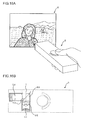
- the liquid crystal panel 1 possesses no polarizer, and the liquid crystal panel 1 is used in combination with a PBS (Polarizing Beam Splitter) block (see Fig. 16B ) .
- the PBS block is a polarizer of a cube form that is fabricated by depositing a polarization isolation film on respective slopes (polarization planes) of rectangular prisms and bonding the prisms such that they contact on the slopes (polarization planes).
- a light having a predetermined oscillation direction is transmitted through the polarization plane and other lights having other predetermined oscillation directions are reflected on the polarization plane.
- the TFT device-formed Si substrate 11 is an Si substrate having formed on the surface thereof TFT devices.
- the TFT device is formed for each pixel electrode. It is an ON/OFF switch that controls charging or supply of charges (pixel signals) in the pixel electrode described hereinbelow.
- the TFT device is ON in a state where a voltage is applied thereto, an electric current flows in the pixel electrode.
- the electric current flows in the pixel electrode, electric charges are accumulated in the pixel electrode and as a result a voltage is applied to a liquid crystal 15.
- the TFT device is turned OFF, the charges accumulated in the pixel electrode will not flow out from the pixel electrode. As a result, the charges accumulated in the pixel electrode are held and the voltage applied to the liquid crystal 15 is held.
- the pixel electrode 12 is provided for each pixel on which description is made hereinafter.
- the pixel electrode 12 is a metal electrode having reflectivity, for example, an aluminum plate. It applies a voltage to the liquid crystal 15.
- the pixel electrodes 12 are formed on the TFT device-formed Si substrate 11 . Aplurality of pixel electrodes 12 is arranged in parallel both horizontally and vertically. The charges supplied to the pixel electrodes 12 are controlled for every pixel electrode corresponding to the ON/OFF state of the TFT device one by one.
- the color filter 13 includes a red (R) filter 13A that transmits only a red light, agreen (G) filter 13B that transmits only a green light, and a blue (B) filter 13C that transmits only a blue light.
- R red
- G agreen
- B blue
- Each of the filters 13A to 13C is a square in shape (see FIG. 2A ).
- the filters 13A to 13C are referred to as square filters generically.
- Each square filter has a dimension of, for example 10 ⁇ m for each side.
- Each of the square filters 13A to 13C is formed on each of the pixel electrodes 12.
- the alignment films 14 and 16 are films that are used to align liquid crystal molecules in respective predetermined directions of the polarization axis.
- the alignment films 14 and 16 have each a thickness of about 0.1 ⁇ m and are made of a high polymer film such as a polyimide film.
- the alignment films 14 and 16 are prepared by performing rubbing treatment on the surface of the above-mentioned high polymer film.
- the rubbing treatment is a treatment in which the surface of a polymer film is rubbed with a cloth wound around a roller.
- the liquid crystal molecules in contact with the alignment films 14 and 16 at the interfaces between the liquid crystal 15 and the alignment films 14 and 16 are aligned in the direction in which the alignment films have been rubbed by the rubbing treatment.
- the direction along which the liquid crystal molecules are aligned is referred to as "rubbing direction".
- the direction along which the surface of the polymer film is rubbed with the cloth wound around the roller is the rubbing direction.
- the rubbing direction of the alignment films 14 and 16 is at an angle of 45°. Since the liquid crystal molecules have the property of tending to align in the same direction, the direction of alignment of liquid crystal molecules gradually changes from the rubbing direction of the alignment film 1A to the rubbing direction of the alignment film 16. As a result, the liquid crystal molecules are aligned as twisted by 45° around an axis along the planar direction of the liquid crystal panel 1. Since the liquid crystal panel 1 is of the reflection type, the light that enters into the liquid crystal 15 travels along a round-trip optical path to go and return in the liquid crystal, thus exhibiting a polarization change corresponding to a 90°-twist.
- the common electrode 17 is a transparent electrode made of ITO (Indium Tin Oxide) or the like disposed opposite to the pixel electrode 12. Also, the common electrode 17 is formed by plasma CVD or sputtering. The common electrode 17 is connected to the groundpotential to generate an electric field in the liquid crystal depending on a difference in potential between the common electrode 16 and the pixel electrodes 12 in which charges are accumulated.
- ITO Indium Tin Oxide
- a single pixel includes the square filters 13A to 13C, the alignment film 14, the liquid crystal 15, the common electrode 17, and the glass substrate 18.
- Each pixel has a square shape.
- a pixel in the liquid crystal panel 1 is displayed/non-displayed.
- the pixel electrode 12 When the pixel electrode 12 is not charged, the pixel is displayed with a light that enters the liquid crystal panel 1. That is, the arrangement of the liquid crystal molecules in the liquid crystal 15 is the above-mentioned 45°-twisted arrangement. Only the linearly polarized light that oscillates in a predetermined direction is allowed to enter a display screen of the liquid crystal panel 1 by a PBS block (not shown) .
- the incident light is transmitted through the glass substrate 18, the common electrode 17, and the alignment film 16. Thereafter, the incident light is transmitted through the liquid crystal 15, the alignment film 14, and the color filter 13 and is reflected by the pixel electrode 12.
- the light reflected by the pixel electrode 12 finally becomes a linearly polarized light having an oscillation direction rotated by 90° with respect to the oscillation direction of the incident linearly polarized light due to the twisted arrangement of the liquid crystal molecules in the liquid crystal 15.
- the linearly polarized light whose oscillation direction has been rotated by 90° is irradiated from the liquid crystal panel 1 to the PBS block (not shown) .
- the transmitted light whose oscillation direction has been rotated by 90° is reflected on the polarization plane of the PBS block and is irradiated in the predetermined direction.
- the pixel electrode 12 when the pixel electrode 12 is charged, the oscillation direction of the light reflected by the liquid crystal panel 1 is not rotated by 90°. As a result, the reflected light from the liquid crystal panel 1 is transmitted through the polarization plane of the PBS block and is not radiated in the predetermined direction.
- control of the supply of charges in the pixel electrode 12 enables reproduction of all the colors by a single pixel, for example, by allowing only the R filter 13A to transmit the light, by allowing only the R filter 13A and the G filter 13B to transmit the light, or the like.
- the control unit that controls the influence on a respective pixel of the electric field by pixel electrodes that are adjacent to the respective pixel is described referring to FIGS. 2A to 4 .
- the pixel electrodes 12 in the R filter 13A and the B filter 13C, respectively, are charged but the pixel electrode 12 in the G filter 13B is not charged.
- FIG. 2A is a diagram illustrating the arrangement of pixels in the first embodiment of the present invention.
- the shape of one pixel is a square as mentioned above, and a delta array is used for displaying colors.
- FIG. 2B is a diagram illustrating the rubbing direction of the alignment film 16 on the common electrode 17 side in the first embodiment.
- the rubbing direction of the alignment film 16 on the common electrode 17 side is a horizontal direction (PL) going from the left to the right of the square filter.
- FIG. 2C is a diagram illustrating the rubbing direction of the alignment film 14 on the pixel electrode 12 side in the first embodiment.
- the rubbing direction of the alignment film 14 on the pixel electrode 12 side is the direction of diagonal line (DL) going from the left below to the right upper of the square filter.
- FIG. 3A is a diagram illustrating the pixel electrode 12 in the first embodiment of the present invention.
- the pixel electrode 12 has a square electrode configuration. On corner portions at the upper left and lower right portions of each pixel electrode, i.e., on the corner portions that are present in a direction orthogonal to the rubbing direction (DL) in the alignment film 14 on the pixel electrode 12 side, respective transparent insulator layers 12E of a triangular shape are formed. The transparent insulator layers 12E are formed on the surface of the pixel electrode 12 on the color filter 13 side.
- the influences by the electric charges of the pixel electrode 12A of the R filter 13A and the pixel electrode 12C of the B filter 13C can be controlled with the transparent insulator layers 12E in the pixel of the G filter 13B.
- the light quantity of the light flux that is transmitted through the G filter 13B and reflected on the polarization plane of the PBS block becomes substantially uniform, so that a reduction in light quantity of the displayed light due to the influences by the pixel electrodes 12 of the adjacent pixels is controlled.
- FIGS. 5A and 5B a comparative example of the liquid crystal panel 1 according to the first embodiment is explained.
- FIG. 5A is a diagram illustrating the pixel electrodes 12 in the comparative example.
- the pixel electrode 12 is not formed of the transparent insulator layer 12E. In this case, the quantity of displayed light of the pixel decreases around the corners in the upper left and lower right of the G filter 13B as shown in FIG. 5B .
- the transparent insulator layers 12E is formed in an area of each of the pixel electrodes 12 on the sides of the direction orthogonal to the rubbing direction (DL) of the alignment film 14 on the pixel electrode 12 side. This can control the influences of the electric fields caused by the adjacent pixel electrodes 12 on the arrangement of the liquid crystal molecules corresponding to each pixel.
- the liquid crystal panel according to a second embodiment of the present invention will be explained.
- the influences of the electric fields by adjacent pixel electrodes can be controlled by forming slits in the common electrode.
- the liquid crystal panel according to the second embodiment differs from the liquid crystal panel 1 according to the first embodiment in the structure of the common electrode .
- the other structures are the same as those in the first embodiment. Accordingly, explanation is focused on the common electrode.
- the common electrode 17 of the liquid crystal panel 1A according to the second embodiment is explained. Explanation hereafter is made assuming that similarly to the first embodiment, only the pixel of the G filter 13B is displayed but the pixels of the R filter 13A and the B filter 13C are not displayed.
- FIG. 6A is a diagram illustrating the pixel electrode in the second embodiment.
- the pixel electrode 12 has a square electrode configuration similarly to the pixel electrode 12 in the first embodiment.
- FIG. 6B is a diagram illustrating the common electrode 17 in the second embodiment.
- Slits 17a are formed in respective parts of the common electrode 17 corresponding to parts along an upper left corner and a lower right corner of each pixel electrode.
- the slits 17a are portions where no ITO film is formed on the glass substrate 18, which parts correspond to the respective parts along the corners that are present in the direction orthogonal to the rubbing direction (DL) of the alignment film 14 on the pixel electrode 12 side.
- Such slits 17a can be formed by forming the common electrode 17 with masking the substrate with a resist.
- the quantity of light that is transmitted through the G filters 13B and radiated after being reflected on the PBS block becomes substantially uniform, so that a reduction in light quantity of the displayed light due to the influences by the pixel electrodes 12 of the adj acent pixels is controlled.
- the slits 17a of the common electrode 17 control a decrease in displayed light quantity by the following operations.
- the slit 17a in the common electrode 17 can prevent the electric field directed toward the common electrode 17 from the pixel electrodes 12A in the pixel of the R filter 13A from expanding near the common electrode 17.
- the slit 17a of the common electrode 17 can prevent the electric field directed toward the common electrode 17 from the pixel electrodes 12C in the pixel of the B filter 13C from expanding near the common electrode 17.
- This can control the influences of the electric fields by the adjacent pixel electrodes on the arrangement of the liquid crystal molecules of the liquid crystal 15 in the pixels of the G filter 13B. As a result, the decrease in the light quantity of the light projected after being refracted by the PBS block is controlled.
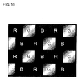
- the liquid crystal panel 100A according to the comparative example includes the common electrode 17 that is free of slits . Therefore, the quantity of light that is radiated after being refracted by the PBS block around the upper left and lower right corners of the G filter 13B decreases as shown in Fig. 10 .
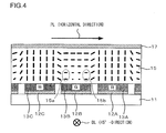
- the liquid crystal panel 100A according to the comparative example includes the common electrode 17 that is free of slits 17a. For this reason, the electric fields directed from the pixel electrode 12A in the pixel of the R filter 13A and the pixel electrode 12C in the pixel of the B filter 13C toward the common electrode 16, there is generated an inclined electric field DI that expands near the common electrode 17.
- the twisted arrangement of the liquid crystal molecules in the liquid crystal 15 in the pixel of the G filter 13B is broken up by the inclined electric field DI, and the light quantity of the reflected light on the polarization plane of the PBS block decreases.
- the liquid crystal panel according to the third embodiment includes pixels (hereafter, referred to as "subpixels”) that emit a white light and are each provided between the pixels equipped with color filters. This makes it possible to prevent a decrease in brightness of a display of the liquid crystal panel due to influences of the electric fields between the pixels.
- FIG. 17 is a diagram illustrating the structure of the liquid crystal panel 1 according to a third embodiment of the present invention.
- the liquid crystal panel 1 shown in Fig. 17 includes the components similar to those of the liquid crystal panel 1 of the first embodiment shown in FIG. 1 .
- the component indicated by reference numeral 13 is called a color filter assembly.
- FIG. 18A is a diagram illustrating a projector 3 that includes the liquid crystal panel 1.
- Reference numeral 2 indicates a projected image that is projected by the projector 3.
- the projector 3 includes a light source 31, a condensation optical system 32, a PBS (Polarizing Beam Splitter) block 33, the liquid crystal panel 1, and a projection optical system 34.
- a driving current is supplied to the LED light source 31 through a harness and a pattern, both of which are not shown.
- the LED light source 31 illuminates the condensation optical system 32 at a brightness corresponding to the supplied electrical current.
- the condensation optical system 32 makes the LED light substantially parallel and radiates the substantially parallel light into the PBS block 33.
- a P-polarized light is transmitted through the PBS block 33 and illuminates the liquid crystal panel 1.
- the radiated light is reflected by the liquid crystal panel 1.
- the reflected light that has been reflected by the liquid crystal panel 1 enters the PBS block 33.
- the incident light is an S-polarized light, which is reflected by the polarization plane 33a of the PBS block 33 and radiated toward the projection optical system 34 as a projected light.
- the light flux that has entered the projection optical system 34 is projected in front of the projector.
- the color filter assembly 13 is an assembly of a plurality of color separation filters that resolve the incident light to a plurality of color components and a plurality of white filters.
- the color filter assembly 13 is formed by a process of photolithography.
- the color filter assembly 13 includes a red (R) filter 13A that transmits only a red light, a green (G) filter 13B that transmits only a green light, a blue (B) filter 13C that transmits only a blue light, and a white (W) filter that transmits all the color lights.
- the shapes of the R filter 13A, G filter 13B, and B filter 13C are hexagons (see FIG. 19A ) .
- the filters 13A to 13C are referred to as color filters generically.
- the shape of the white filter 13D is a parallelogram (see FIG. 19A ) .
- the color filters 13A to 13C and the white filter 13D are formed on each of the pixel electrodes 12.
- the color filters 13A to 13C are in a delta array as shown in FIG. 19A . That is, the R filter 13A, the G filter 13B, and the B filter 13C are arranged so that each center position thereof together may define a triangle. More particularly, one pixel includes one color filter 13A1, one color filter 13B1, and one color filter 13C1 as well as the TFT device-formed Si substrate 11, the pixel electrode 12, the alignment film 14, the liquid crystal 15, the alignment film 16, the common electrode 17, and the glass substrate 18, each corresponding to each of the color filters 13A1, 13B1, and 13C1.
- All the colors can be reproduced with a single pixel by combining lights that are transmitted through the R filter 13A, the G filter 13B, and the B filter 13C, respectively, based on the principle of additive color mixing.
- a single rectangular filter has a longer direction (horizontal direction in FIG. 19A ) dimension of, for example, 10 ⁇ m and a shorter direction (vertical direction in FIG. 19A ) dimension of, for example, 7.5 ⁇ m.
- the white filters 13D is arranged such that the longer sides thereof are adjacent to sides of the color filters 13A to 13C in a predetermined direction.
- One subpixel includes one white filter 13D and the TFT device-formed Si substrate 11, the pixel electrode 12, the alignment film 14, the liquid crystal 15, the alignment film 16, the common electrode 17, and the glass substrate 18, each corresponding to the white filter 13D.
- the pixel of the R filter 13A is called “R pixel”
- the pixel of the G filter is called “G pixel”
- the pixel of the B filter 13C is called "B pixel”.
- the liquid crystal panel 1 is constituted as an assembly of the R, G, and B pixels and subpixels.
- each pixel in the liquid crystal panel 1 is made displayed/non-displayed on the projection plane.
- the pixel electrode 12 is not charged.
- the liquid crystal molecules in the liquid crystal 15 are in a 45°-twisted arrangement.
- the PBS block 33 When the light from the LED light source 31 is radiated into the PBS block 33, only the P-polarized light is incident to the liquid crystal panel 1. The P-polarized light is transmitted through the glass substrate 18, the common electrode 17, and the alignment film 16. Thereafter, the P-polarized light is transmitted through the liquid crystal 15, the alignment film 14, and the color filters (white filter) 13A to 13C (13D) and is reflected by the pixel electrode 12.
- the light reflected by the pixel electrode 12 finally becomes an S-polarized light having an oscillation direction rotated by 90° with respect to the oscillation direction of the incident P-polarized light due to the twisted arrangement of the liquid crystal molecules in the liquid crystal 15.
- the P-polarized light is reflected on the polarization plane 33a, and is radiated from the projector 3.
- the reflection pixel electrode 12 is charged.
- the liquid crystal molecules in the liquid crystal 15 are arranged in the direction of the electric field.
- the oscillation direction of the P-polarized light that has been reflected by the liquid crystal panel 1 is not rotated by 90°, so that the light reflected by the liquid crystal panel 1 is a P-polarized light, which is transmitted through the PBS block without being reflected on the polarization plane 33a of the PBS block, so that it is not radiated from the projector 3.
- control of the supply of charges in the pixel electrode 12 enables reproduction of all the colors by a single pixel, for example, by allowing only the R pixel to be displayed on the projection plane, by allowing only the R pixel and the G pixel to be displayed on the projection plane, or the like.
- control of the supply of charges in the pixel electrode 12 enables switching of display/non-display of the subpixel on the projection plane.
- the control unit that controls the influences on a respective pixel of the electric field by pixel electrodes that are adjacent to the respective pixel is described.
- explanation is made on the case where only the pixel of the G filter 13B is displayed on the projection plane but the R and B pixels are not displayed.
- the pixel electrodes 12 in the R pixel and the B pixel, respectively, are charged but the pixel electrode 12 in the G pixel is not charged.
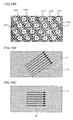
- FIG. 19A is a diagram illustrating the color filter assembly 13 in the third embodiment of the present invention.
- the shape of the color filters 13A to 13C is a hexagon as mentioned above and the color filters 13A to 13C are in a delta array.
- the shape of the white filter 13D is a parallelogram, and the white filter 13D is arranged so that the longer sides thereof may contact the sides in the predetermined direction of the color filters 13A to 13C.
- FIG. 19B is a diagram illustrating the rubbing direction of the alignment film 14 on the pixel electrode 12 side in the embodiment of the present invention.
- the rubbing direction of the alignment film 14 on the pixel electrode 12 side is the direction of a diagonal line (DL) going from the lower left to the upper right of the color filters 13A to 13C.
- DL diagonal line
- 19C is a diagram illustrating the rubbing direction of the alignment film 16 on the common electrode 17 side in the third embodiment of the present invention.
- the rubbing direction of the alignment film 16 on the common electrode 17 side is a direction (PL) at an angle of 45° to the rubbing direction of the alignment film 14.
- the longer sides of the white filter 13D are arranged so as to contact the sides of the color filters 13A to 13C, located in a direction substantially orthogonal to the rubbing direction (DL) of the alignment film 14 on the pixel electrode 12 side as shown in FIGS. 19A and 19B .
- the orientation of the longer sides of the white filter 13D is the same as the rubbing direction (DL) of the alignment film 14 on the pixel electrode 12 side.
- FIG. 20 is an enlarged view of a projected image 2 that is projected on the projection plane.
- the displayed light quantity of the G pixel is reduced because of the influences of the supplied electric charges in the pixel electrodes of the adjacent R pixel and B pixel (see FIG. 21B to be detailed later).
- the reduction of luminance in the display of G pixel can be controlled by causing the subpixels of the white filters 13D1 and 13D2 whose longer sides are in contact with the G filter 13B to emit light.
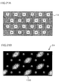
- FIGS. 21A and 21B a comparative example of the liquid crystal panel 1 according to the third embodiment of the present invention is explained.
- FIG. 21A is a diagram illustrating the color filter assembly 13 in the comparative example.
- the color filters have each a rectangular shape, and no white filter is formed in the color filter assembly 13.
- the displayed light quantity of the pixel decreases around the upper left and lower right corners of the G filter 13B as shown in an enlarged view of the projected image 2A in FIG. 21B and thus the displayed light quantity of the pixel is decreased.
- the displayed light quantity is decreased by the following operations.
- the pixel electrodes 12A and 12C are charged to align the liquid crystal molecules in a direction from the pixel electrodes 12A and 12C toward the common electrode 17 as shown in FIG. 22A .
- the electric fields generated by the pixel electrodes 12A and 12C are directed toward the pixel electrode 12B of the Gpixel as well as toward the common electrode 17. Therefore, a 45°-twisted array of the liquid crystal molecules 15a and 15b of the pixel electrode 12B near the G pixel is broken up.
- the oscillation direction is not rotated by 90°, so that the displayed light quantity of the G pixel is decreased.
- corner parts of the G pixel on the sides in the direction substantially orthogonal to the rubbing direction (DL) on the pixel electrode 12B side the electric fields from the two pixels that are in contact with the corners are combined to generate a strong electric field in a direction substantially orthogonal to the rubbing direction (DL), so that the extent in which the 45°-twisted array of the liquid crystal molecules is broken up is enlarged. This would cause the displayed light quantity of the pixel to decrease around the upper left and lower right corners of the G filter 17B as shown in FIG. 21B .
- the level of a reduction in displayed light quantity of the G pixel is small as compared with the comparative example. This would be due to provision of the pixel electrode 12D of the white filter 13B between the pixel electrode 12A of the R pixel and the pixel electrode 12C of the B pixel as shown in FIG. 22B , which is considered to alleviate the influences of the electric fields on the G pixel from the pixel electrodes 12A and 12C of the R pixel and the B pixel, respectively.
- the subpixel plays the role of an electric field alleviation area between the pixels. For example, in FIG.
- the liquid molecules near the pixel electrode 12D of the white filter 13D are influenced by the electric fields from the pixel electrode 12A of the R pixel and the pixel electrodes 12C of the B pixel.
- the spacing between the pixel electrode 12A and the pixel electrode 12C increases and the liquid crystal molecules on the pixel electrode 12B of the G pixel are less influenced by the pixel electrode 12A of the R pixel and the pixel electrode 12C of the B pixel.
- the liquid crystal panel device 100 includes the liquid crystal panel 1 and a liquid crystal panel control circuit 110.
- the liquid crystal panel control circuit 110 outputs a driving signal to the liquid crystal panel 1 and controls the pixels and the subpixels. As a result, the liquid crystal panel 1 generates an image according to the driving signal.
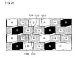
- the liquid crystal panel control circuit 110 renders the gradation of brightness of the subpixel 62D sandwiched by the two color pixels 62A and 62B equal to or less than each of the gradations of brightness of the two color pixels 62A and 62B when displays of the two adjacent color pixels 62A and 62B sandwiching the subpixel 62D are other than black displays (i.e., gradation of brightness is 0) .
- This makes it possible to prevent the display of the liquid crystal panel 1 from becoming paler by displaying the subpixel 62D.
- the liquid crystal panel control circuit 110 sets the gradation of the subpixel 62D to a value of 100 or less.
- the liquid crystal panel control circuit 110 sets the gradation of the brightness of the subpixel 63D to the same value as them. As a result, the balance of the brightness of the subpixel 63D with respect to the surrounding color pixels 63A to 63C can be maintained. For example, when the gradations of the color pixels 63A to 63C are 100, the liquid crystal panel control circuit 110 adjusts the gradation of the subpixel 62D to 100.
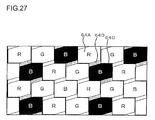
- the liquid crystal panel control circuit 110 increases the value of the gradation of brightness of the subpixel 64D to more than 0. Since the intensity of electric field generated by the pixel electrode 12D of the subpixel 64D is lower than the intensity of electric field generated by the pixel electrode 12C of the color pixel 64C because of a large value of gradation of the pixels, the influence of he electric field generated by the color pixel 64C on the color pixel 64A can be weakened. Especially, the influence on pixels that are adjacent in a direction orthogonal to the rubbing direction (DL) on the pixel electrode 12 side is great.
- the liquid crystal panel control circuit 110 makes the value of gradation of brightness of the subpixel 64D greater than 0 when the color pixel 64C that is in contact with a longer side of the subpixel 64D of a tetragonal shape with longer sides is displayed in black. That is, the liquid crystal panel control circuit 110 increases the value of the gradation of brightness of the subpixel 64D formed in a direction substantially orthogonal to the rubbing direction (DL) on the pixel electrode 12 side to be greater than 0. For example, when the gradation of the color pixel 63C is 0, the liquid crystal panel control circuit 110 adjusts the gradation of the subpixel 64D to be equal to or more than 1.
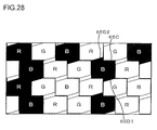
- the present invention is not limited to the case where when the adj acent color pixel 64C is displayed in black (i.e., the value of gradation of brightness is 0), the liquid crystal panel control circuit 110 sets the value of gradation of brightness of the adjacent subpixel 64C (the value of the step of brightness is 0) to be greater than 0.
- the liquid crystal panel control circuit may set the values of gradations of brightness of the subpixels 65D1 and 65D2 as shown in FIG. 28 . The purpose of this is to prevent the white subpixels 65D1 and 65D2 from seeming to come off from among the black color pixels 65C.
- the first to the third embodiments as described above may be modified as follows.
Landscapes
- Physics & Mathematics (AREA)
- Nonlinear Science (AREA)
- Spectroscopy & Molecular Physics (AREA)
- Mathematical Physics (AREA)
- Chemical & Material Sciences (AREA)
- Crystallography & Structural Chemistry (AREA)
- General Physics & Mathematics (AREA)
- Optics & Photonics (AREA)
- Liquid Crystal (AREA)
Abstract

Description
- The disclosure of the following propriety applications are herein incorporated by reference:
- Japanese Patent Application No.
2008-077854 filed March 25, 2008 - Japanese Patent Application No.
2008-090742 filed March 31, 2008 - Japanese Patent Application No.
2008-112559 filed April 23, 2008 - The present invention relates to a liquid crystal panel, a liquid crystal panel device, a display device, and a projector.
- Japanese Laid-open Patent Publication No.
06-118447 - Miniaturization of pixels (or a decrease in pixel size) makes it necessary to suppress influences of crosstalk by pixel electrodes as well as crosstalk by signal lines.
- According to the 1st aspect of the present invention, a liquid crystal panel comprises: a liquid crystal containing liquid crystal molecules; a plurality of pixel electrodes that is capable of applying electric fields to the liquid crystal; a common electrode opposite to the plurality of the pixel electrodes through the liquid crystal; a first rubbing means for aligning the liquid crystal molecules in a first direction at an interface of the liquid crystal on a side of the pixel electrode; and a second rubbing means for aligning the liquid crystal molecules in a second direction at an interface of the liquid crystal on a side of the common electrode, wherein a transparent insulator layer is formed on an area on a side in a direction orthogonal to the first direction in the pixel electrode.
- According to the 2nd aspect of the present invention, in a liquid crystal panel according to the 1st aspect, it is preferred that each of the pixel electrodes has a rectangular shape, the first direction is a direction of a diagonal line of the pixel electrode, pixels corresponding to the pixel electrodes are arranged in a delta array, and the transparent insulator layer is formed at a corner in a direction orthogonal to the first direction in the pixel electrode.
- According to the 3rd aspect of the present invention, in a liquid crystal panel according to the 2nd aspect, it is preferred that the transparent insulator layer is further formed in an area of other pixel electrodes that are adjacent to the corner in the direction orthogonal to the first the direction.
- According to the 4th aspect of the present invention, in a liquid crystal panel according to any one of the 1st through the 3rd aspects, it is preferred that the common electrode includes an electric field control means for controlling an influence of an electric field generated between the common electrode and the first pixel electrode among the pixel electrodes on the liquid crystal molecules arranged on the side of the common electrode among the liquid crystal molecules on a second pixel electrode adjacent to the first pixel electrode.
- According to the 5th aspect of the present invention, a liquid crystal panel including a plurality of rectangular pixels in a delta array, the liquid crystal panel comprises:
- a liquid crystal containing liquid crystal molecules; a
- plurality of rectangular pixel electrodes that is capable of applying electric fields to the liquid crystal; a common
- electrode opposite to the plurality of the pixel electrodes through the liquid crystal; a first rubbing means for aligning the liquid crystal molecules in a direction of diagonal line of the pixel electrode at an interface of the liquid crystal on a side of the pixel electrode; and a second rubbing means for aligning the liquid crystal molecules in a second direction at an interface of the liquid crystal on the side of the common electrode, wherein the common electrode includes an electric field control means for controlling an influence of an electric field generated between the common electrode and the first pixel electrode among the pixel electrodes on the liquid
- crystal molecules arranged on the side of the common electrode among the liquid crystal molecules on a second pixel electrode adjacent to the first pixel electrode.
- According to the 6th aspect of the present invention, in a liquid crystal panel according to the 4th or the 5th aspect, it is preferred that the electric field control means includes a slit-like non-conductive part formed on the common electrode along a corner in a direction orthogonal to the first direction in the pixel electrode.
- According to the 7th aspect of the present invention, in a liquid crystal panel according to the 4th or the 5th aspect, it is preferred that the electric field control means includes a transparent insulator layer formed on the common electrode along a corner in a direction orthogonal to the first direction in the pixel electrode.
- According to the 8th aspect of the present invention, a liquid crystal panel comprises: a liquid crystal of which a direction of alignment is set; a color filter including a plurality of color separation filters that separates incident light into a plurality of color components; a plurality of white filters adjacent to the color filters as sandwiched between at least two of the color separation filters among the plurality of the color separation filters; and a light quantity control electrode that controls light quantity of light that is transmitted through the color separation filters and the white filter by controlling the alignment of the liquid crystal, wherein a pixel array for a display includes a plurality of pixels that corresponds to the plurality of color separation filters and a plurality of pixels that corresponds to the plurality of white filters.
- According to the 9th aspect of the present invention, in a liquid crystal panel according to the 8th aspect, it is preferred that the light quantity control electrode includes a pixel electrode provided for each of the color separation filters and the white filters and a common electrode common to the pixel electrodes.
- According to the 10th aspect of the present invention, in a liquid crystal panel according to the 9th aspect, it is preferred that the common electrode is provided opposite to the plurality of pixel electrodes through the liquid crystal, and the liquid crystal panel comprises: a first alignment film that is provided on a side of the common electrode and that aligns the liquid crystal in the first direction; and a second alignment film that is provided on a side of the pixel electrode and that aligns the liquid crystal in the second direction, and wherein the white filter is arranged adjacent to the color separation filters in a direction substantially orthogonal to the second direction.
- According to the 11th aspect of the present invention, in a liquid crystal panel according to the 9th aspect, it is preferred that the white filter is arranged in an area where the light quantity of a light that is transmitted through the pixel without the white filter is decreased to a value smaller than a predetermined value due to turbulence of the alignment of the liquid crystal by a pixel signal applied to the adjacent pixel electrodes.
- According to the 12th aspect of the present invention, in a liquid crystal panel according to any one of the 8th through 11th aspects, it is preferred that the plurality of color separation filters is arranged in a delta array, and a shape of the white filter is a parallelogram, and a length of a diagonal line of the white filter is 1/2 of a length of a longer side of the parallelogram when the rectangular shape is formed by a combination of a shorter side of the white filter, the diagonal line of the white filter, and a side of the color separation filter that is not in contact with the white filter.
- According to the 13th aspect of the present invention, a liquid crystal panel device comprises : a liquid crystal panel according to any one of the 8th through 12th aspects; and a pixel signal generation means for generating a pixel signal applied to the light quantity control electrode, wherein the pixel signal generation means generates the pixel signal such that a value of a gradation of brightness of the pixel displayed by the white filter is equal to or smaller than each of values of gradation of brightness of pixels displayed by adjacent two color separation filters sandwiching the white filter when the pixels displayed by adjacent two color separation filters sandwiching the white filter displays colors other than black.
- According to the 14th aspect of the present invention, a liquid crystal panel device comprises : a liquid crystal panel according to any one of the 8th through the 12th aspects; and a pixel signal generation means for generating a pixel signal applied to the light quantity control electrode, wherein the pixel signal generation means generates the pixel signal such that a value of gradation of brightness of the pixel displayed by the white filter is equal to a value of gradation of brightness of the pixels displayed by four color separation filters, when three of four color separation filters surrounding the white filter are color separation filters corresponding to respective color components and values of gradation of brightness of respective pixels displayed by the four color separation filters are equal.
- According to the 15th aspect of the present invention, a liquid crystal panel device comprises : a liquid crystal panel according to any one of the 8th through the 12th aspects; and a pixel signal generation means for generating a pixel signal applied to the light quantity control electrode, wherein the pixel signal generation means generates the pixel signal such that a value of a gradation of brightness of the pixel displayed by the white filter is larger than 0, when a shape of the white filter is a quadrangle having longer sides and the pixel displayed by the color separation filter that is in contact with the longer sides of the white filter displays black.
- According to the 16th aspect of the present invention, a liquid crystal panel device comprises : a liquid crystal panel according to any one of the 8th through the 12th aspects; and a pixel signal generation means for generating a pixel signal applied to the light quantity control electrode, wherein the pixel signal generation means generates the pixel signal such that a value of a gradation of brightness of the pixel displayed by the white filter is larger than 0, when the color separation filter corresponding to the pixel that displays black is in contact with the white filter on a side in a direction substantially orthogonal to the first rubbing direction.
- According to the 17th aspect of the present invention, a liquid crystal panel device comprises : a liquid crystal panel according to any one of the 8th through the 12th aspects; and a pixel signal generation means for generating a pixel signal applied to the light quantity control electrode, wherein the pixel signal generation means generates the pixel signal such that a value of a gradation of brightness of the pixel displayed by the white filter is 0, when a shape of the white filter is a quadrangle having longer sides and the pixel displayed by the color separation filter that is in contact with the longer sides of the white filter displays black.
- According to the 18th aspect of the present invention, a display device comprises a liquid crystal panel according to any one of the 1st through the 17th aspects.
- According to the 19th aspect of the present invention, a projector comprises a liquid crystal panel according to any one of the 1st through 17th aspects.
-
-
FIG. 1 is a diagram illustrating the structure of a liquid crystal panel according to a first embodiment of the present invention; -
FIGS. 2A to 2C are diagrams illustrating the rubbing directions of alignment films according to the first embodiment of the present invention, withFIG. 2A showing an example of arrangement of the color filters in the liquid crystal panel, -
FIG. 2B showing the rubbing direction of the alignment film on the common electrode side, andFIG. 2C showing the rubbing direction of the alignment film on the color filter side; -
FIG. 3A is a diagram illustrating pixel electrodes and -
FIG. 3B is a diagram illustrating a display of the liquid crystal panel; -
FIG. 4 is a diagram illustrating the arrangement of liquid crystal molecules influenced by the electric fields from the pixel electrodes of adjacent pixels; -
FIG. 5A is a diagram illustrating pixel electrodes in a comparative example of the first embodiment andFIG. 5B is a diagram illustrating a liquid crystal panel of the comparative example. -
FIG. 6A is a diagram illustrating pixel electrodes in a second embodiment andFIG. 6B is a diagram illustrating a common electrode in the second embodiment; -
FIG. 7 is a diagram illustrating a display of the liquid crystal panel in the second embodiment; -
FIGS. 8A and 8B are diagrams illustrating electric fields generated by the pixel electrodes, withFIG. 8A showing the electric fields generated when the common electrode is provided with slits andFIG. 8B showing the electric fields generated when the common electrode is not provided with slits; -
FIG. 9 is a diagram illustrating the common electrode in a comparative example of the second embodiment; -
FIG. 10 is a diagram illustrating a display of the liquid crystal panel in the comparative example of the second embodiment; -
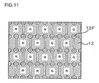
FIG. 11 is a diagram illustrating a modification of a transparent insulator layer in the first embodiment; -
FIG. 12A is a diagram illustrating pixel electrodes in the second embodiment andFIG. 12B is a diagram illustrating a modification of slits formed in the common electrode according to the second embodiment; -
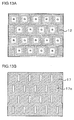
FIG. 13A is a diagram illustrating pixel electrodes according to the second embodiment andFIG. 13B is a diagram illustrating a modification of slits formed in the common electrode according to the second embodiment; -
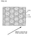
FIG. 14 is a diagram illustrating the transparent insulator layers in the case where the shape of the pixel electrodes is hexagonal; -
FIG. 15A is a diagram illustrating pixel electrodes each having a hexagonal shape andFIG. 15B is a diagram illustrating slits formed in the common electrode in the case where the shape of the pixel electrodes is hexagonal; -
FIGS. 16A and 16B are diagrams illustrating a projector that includes the liquid crystal panel of the present invention; -
FIG. 17 is a diagram illustrating the structure of a liquid crystal panel according to a third embodiment of the present invention; -
FIGS. 18A and 18B are diagrams illustrating a projector that includes the liquid crystal panel of the present invention; -
FIGS. 19A to 19C are diagrams illustrating the rubbing directions of alignment films according to the third embodiment of the present invention, withFIG. 19A showing an example of arrangement of the color filters in the liquid crystal panel, -
FIG. 19B showing the rubbing direction of the alignment film on the color filter side, andFIG. 19C showing the rubbing direction of the alignment film on the common electrode side; -
FIG. 20 is a diagram illustrating pixels projected on a projection plane in the third embodiment; -
FIG. 21A and FIG. 21B are diagrams illustrating a comparative example of the third embodiment, withFIG. 21A illustrating a color filter assembly andFIG. 21B being a diagram illustrating an example of a display of the liquid crystal panel; -
FIG. 22A and FIG. 22B are diagrams illustrating the arrangement of liquid crystal molecules, withFIG. 22A showing the arrangement of liquid crystal molecules in a comparative example of the third embodiment andFIG. 22B showing the arrangement of liquid crystal molecules in the third embodiment; -
FIG. 23 is a diagram illustrating a color coordinate; -
FIG. 24 is a diagram illustrating a liquid crystal panel device according to the third embodiment of the present invention; -
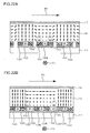
FIG. 25 is a diagram illustrating an example of gradation of brightness in a display of subpixels; -
FIG. 26 is a diagram illustrating an example of gradation of brightness in a display of subpixels; -
FIG. 27 is a diagram illustrating an example of gradation of brightness in a display of subpixels; -
FIG. 28 is a diagram illustrating an example of gradation of brightness in a display of subpixels; -
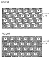
FIGS.29A and 29B are diagrams illustrating a modification of the shape of white filters; -
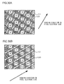
FIGS.30A and 30B are diagrams illustrating a modification of the shape of white filters; -
FIG. 31 is a diagram illustrating the length of a diagonal line of the white filter; -
FIGS. 32A to 32C are diagrams illustratingmodifications of the arrangement of pixels; -
FIGS. 33A and 33B are diagrams illustrating modifications of the arrangement of subpixels; and -
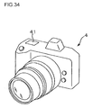
FIG. 34 is a diagram illustrating a display device provided with the liquid crystal panel of the present invention. - Hereinafter, preferred embodiments of the present invention will be explained with reference to the attached drawings.
- In the liquid crystal panel in the first embodiment, the influences by pixel electrode of adjacent pixels can be controlled by forming a transparent insulator layer on each pixel electrode to be detailed later.
-
FIG. 1 is a diagram illustrating the structure of aliquid crystal panel 1 according to a first embodiment of the present invention. Theliquid crystal panel 1 according to the first embodiment of the present invention is a reflection type liquid crystal panel, which realizes its function as a display device with a light that enters theliquid crystal panel 1. Theliquid crystal panel 1 is constituted by a TN (Twisted Nematic) type liquid crystal. In theliquid crystal panel 1, the liquid crystal molecules are arranged such that they are twisted by 90° around an axis along a planar direction of theliquid crystal panel 1 upon reflection. Theliquid crystal panel 1 according to the first embodiment of the present invention is a liquid crystal panel of an active matrix system that includes TFTs (Thin Film Transistors). Each of the pixels in theliquid crystal panel 1 is provided with an ON/OFF switch constituted by the TFT. - The
liquid crystal panel 1 includes a TFT device-formedSi substrate 11, apixel electrode 12, acolor filter 13, analignment film 14, aliquid crystal 15, analignment film 16, acommon electrode 17, and a glass substrate 18. Theliquid crystal panel 1 possesses no polarizer, and theliquid crystal panel 1 is used in combination with a PBS (Polarizing Beam Splitter) block (seeFig. 16B ) . The PBS block is a polarizer of a cube form that is fabricated by depositing a polarization isolation film on respective slopes (polarization planes) of rectangular prisms and bonding the prisms such that they contact on the slopes (polarization planes). Of the lights that have entered the PBS block, a light having a predetermined oscillation direction is transmitted through the polarization plane and other lights having other predetermined oscillation directions are reflected on the polarization plane. - The TFT device-formed
Si substrate 11 is an Si substrate having formed on the surface thereof TFT devices. The TFT device is formed for each pixel electrode. It is an ON/OFF switch that controls charging or supply of charges (pixel signals) in the pixel electrode described hereinbelow. When the TFT device is ON in a state where a voltage is applied thereto, an electric current flows in the pixel electrode. When the electric current flows in the pixel electrode, electric charges are accumulated in the pixel electrode and as a result a voltage is applied to aliquid crystal 15. When the TFT device is turned OFF, the charges accumulated in the pixel electrode will not flow out from the pixel electrode. As a result, the charges accumulated in the pixel electrode are held and the voltage applied to theliquid crystal 15 is held. If the TFT device is turned ON thereafter in a state where no voltage is applied, an electric current flows from the pixel electrode. When the electric current flows from the pixel electrode, the charges accumulated in the pixel electrode are discharged, so that application of voltage to theliquid crystal 15 is cancelled. - The
pixel electrode 12 is provided for each pixel on which description is made hereinafter. Thepixel electrode 12 is a metal electrode having reflectivity, for example, an aluminum plate. It applies a voltage to theliquid crystal 15. Thepixel electrodes 12 are formed on the TFT device-formedSi substrate 11 . Aplurality ofpixel electrodes 12 is arranged in parallel both horizontally and vertically. The charges supplied to thepixel electrodes 12 are controlled for every pixel electrode corresponding to the ON/OFF state of the TFT device one by one. - The
color filter 13 includes a red (R)filter 13A that transmits only a red light, agreen (G)filter 13B that transmits only a green light, and a blue (B)filter 13C that transmits only a blue light. Each of thefilters 13A to 13C is a square in shape (seeFIG. 2A ). Hereafter, thefilters 13A to 13C are referred to as square filters generically. Each square filter has a dimension of, for example 10 µm for each side. Each of thesquare filters 13A to 13C is formed on each of thepixel electrodes 12. - The
alignment films alignment films alignment films alignment films liquid crystal 15 and thealignment films alignment films alignment film 16. As a result, the liquid crystal molecules are aligned as twisted by 45° around an axis along the planar direction of theliquid crystal panel 1. Since theliquid crystal panel 1 is of the reflection type, the light that enters into theliquid crystal 15 travels along a round-trip optical path to go and return in the liquid crystal, thus exhibiting a polarization change corresponding to a 90°-twist. - The
common electrode 17 is a transparent electrode made of ITO (Indium Tin Oxide) or the like disposed opposite to thepixel electrode 12. Also, thecommon electrode 17 is formed by plasma CVD or sputtering. Thecommon electrode 17 is connected to the groundpotential to generate an electric field in the liquid crystal depending on a difference in potential between thecommon electrode 16 and thepixel electrodes 12 in which charges are accumulated. - A single pixel includes the
square filters 13A to 13C, thealignment film 14, theliquid crystal 15, thecommon electrode 17, and the glass substrate 18. Each pixel has a square shape. - The principle in which a pixel in the
liquid crystal panel 1 is displayed/non-displayed will be explained with reference toFIG. 1 . When thepixel electrode 12 is not charged, the pixel is displayed with a light that enters theliquid crystal panel 1. That is, the arrangement of the liquid crystal molecules in theliquid crystal 15 is the above-mentioned 45°-twisted arrangement. Only the linearly polarized light that oscillates in a predetermined direction is allowed to enter a display screen of theliquid crystal panel 1 by a PBS block (not shown) . The incident light is transmitted through the glass substrate 18, thecommon electrode 17, and thealignment film 16. Thereafter, the incident light is transmitted through theliquid crystal 15, thealignment film 14, and thecolor filter 13 and is reflected by thepixel electrode 12. - The light reflected by the
pixel electrode 12 finally becomes a linearly polarized light having an oscillation direction rotated by 90° with respect to the oscillation direction of the incident linearly polarized light due to the twisted arrangement of the liquid crystal molecules in theliquid crystal 15. The linearly polarized light whose oscillation direction has been rotated by 90° is irradiated from theliquid crystal panel 1 to the PBS block (not shown) . The transmitted light whose oscillation direction has been rotated by 90° is reflected on the polarization plane of the PBS block and is irradiated in the predetermined direction. - On the other hand, when the
pixel electrode 12 is charged, the oscillation direction of the light reflected by theliquid crystal panel 1 is not rotated by 90°. As a result, the reflected light from theliquid crystal panel 1 is transmitted through the polarization plane of the PBS block and is not radiated in the predetermined direction. - As mentioned above, control of the supply of charges in the
pixel electrode 12 enables reproduction of all the colors by a single pixel, for example, by allowing only theR filter 13A to transmit the light, by allowing only theR filter 13A and theG filter 13B to transmit the light, or the like. - The control unit that controls the influence on a respective pixel of the electric field by pixel electrodes that are adjacent to the respective pixel is described referring to
FIGS. 2A to 4 . In this embodiment, explanation is made on the case where only the pixel of theG filter 13B is displayed but the pixels of theR filter 13A and theB filter 13C are not displayed. In this case, thepixel electrodes 12 in theR filter 13A and theB filter 13C, respectively, are charged but thepixel electrode 12 in theG filter 13B is not charged. -
FIG. 2A is a diagram illustrating the arrangement of pixels in the first embodiment of the present invention. The shape of one pixel is a square as mentioned above, and a delta array is used for displaying colors.FIG. 2B is a diagram illustrating the rubbing direction of thealignment film 16 on thecommon electrode 17 side in the first embodiment. The rubbing direction of thealignment film 16 on thecommon electrode 17 side is a horizontal direction (PL) going from the left to the right of the square filter.FIG. 2C is a diagram illustrating the rubbing direction of thealignment film 14 on thepixel electrode 12 side in the first embodiment. The rubbing direction of thealignment film 14 on thepixel electrode 12 side is the direction of diagonal line (DL) going from the left below to the right upper of the square filter. -
FIG. 3A is a diagram illustrating thepixel electrode 12 in the first embodiment of the present invention. Thepixel electrode 12 has a square electrode configuration. On corner portions at the upper left and lower right portions of each pixel electrode, i.e., on the corner portions that are present in a direction orthogonal to the rubbing direction (DL) in thealignment film 14 on thepixel electrode 12 side, respectivetransparent insulator layers 12E of a triangular shape are formed. Thetransparent insulator layers 12E are formed on the surface of thepixel electrode 12 on thecolor filter 13 side. The influences by the electric charges of thepixel electrode 12A of theR filter 13A and thepixel electrode 12C of theB filter 13C can be controlled with thetransparent insulator layers 12E in the pixel of theG filter 13B. As a result, as shown inFIG. 3B , the light quantity of the light flux that is transmitted through theG filter 13B and reflected on the polarization plane of the PBS block becomes substantially uniform, so that a reduction in light quantity of the displayed light due to the influences by thepixel electrodes 12 of the adjacent pixels is controlled. - As shown in
FIG. 4 , power to rotate theliquid crystal molecules G filter 13B by 90° is generated by the influences of the electric fields from thepixel electrode 12A of theR filter 13A and thepixel electrode 12C of theB filter 13C and the twisted arrangement of the liquid crystal molecules is broken up. However, the influences of the electric fields from thepixel electrode 12A of theR filter 13A and thepixel electrode 12C of theB filter 13C are weakened by forming thetransparent insulator layer 12E to thepixel electrode 12B, and the breaking up of the twisted arrangement of the liquid crystal molecules is controlled. - Referring to
FIGS. 5A and 5B , a comparative example of theliquid crystal panel 1 according to the first embodiment is explained. Hereafter, explanation is made assuming that the rubbing directions of thealignment films FIG. 5A is a diagram illustrating thepixel electrodes 12 in the comparative example. Thepixel electrode 12 is not formed of thetransparent insulator layer 12E. In this case, the quantity of displayed light of the pixel decreases around the corners in the upper left and lower right of theG filter 13B as shown inFIG. 5B . - According to the first embodiment as described above, the following advantageous effect can be obtained.
- The
transparent insulator layers 12E is formed in an area of each of thepixel electrodes 12 on the sides of the direction orthogonal to the rubbing direction (DL) of thealignment film 14 on thepixel electrode 12 side. This can control the influences of the electric fields caused by theadjacent pixel electrodes 12 on the arrangement of the liquid crystal molecules corresponding to each pixel. - The liquid crystal panel according to a second embodiment of the present invention will be explained. In this liquid crystal panel, the influences of the electric fields by adjacent pixel electrodes can be controlled by forming slits in the common electrode.
- The liquid crystal panel according to the second embodiment differs from the
liquid crystal panel 1 according to the first embodiment in the structure of the common electrode . The other structures are the same as those in the first embodiment. Accordingly, explanation is focused on the common electrode. - Referring to
FIGS. 6A to 9 , thecommon electrode 17 of the liquid crystal panel 1A according to the second embodiment is explained. Explanation hereafter is made assuming that similarly to the first embodiment, only the pixel of theG filter 13B is displayed but the pixels of theR filter 13A and theB filter 13C are not displayed. -
FIG. 6A is a diagram illustrating the pixel electrode in the second embodiment. Thepixel electrode 12 has a square electrode configuration similarly to thepixel electrode 12 in the first embodiment.FIG. 6B is a diagram illustrating thecommon electrode 17 in the second embodiment.Slits 17a are formed in respective parts of thecommon electrode 17 corresponding to parts along an upper left corner and a lower right corner of each pixel electrode. In other words, theslits 17a are portions where no ITO film is formed on the glass substrate 18, which parts correspond to the respective parts along the corners that are present in the direction orthogonal to the rubbing direction (DL) of thealignment film 14 on thepixel electrode 12 side.Such slits 17a can be formed by forming thecommon electrode 17 with masking the substrate with a resist. As a result, as shown inFIG. 7 , the quantity of light that is transmitted through the G filters 13B and radiated after being reflected on the PBS block becomes substantially uniform, so that a reduction in light quantity of the displayed light due to the influences by thepixel electrodes 12 of the adj acent pixels is controlled. - The
slits 17a of thecommon electrode 17 control a decrease in displayed light quantity by the following operations. As shown inFIG. 8A , theslit 17a in thecommon electrode 17 can prevent the electric field directed toward thecommon electrode 17 from thepixel electrodes 12A in the pixel of theR filter 13A from expanding near thecommon electrode 17. In addition, theslit 17a of thecommon electrode 17 can prevent the electric field directed toward thecommon electrode 17 from thepixel electrodes 12C in the pixel of theB filter 13C from expanding near thecommon electrode 17. This can control the influences of the electric fields by the adjacent pixel electrodes on the arrangement of the liquid crystal molecules of theliquid crystal 15 in the pixels of theG filter 13B. As a result, the decrease in the light quantity of the light projected after being refracted by the PBS block is controlled. - Referring to
FIG. 9 , a comparative example of the liquid crystal panel 1A according to the second embodiment is explained. Thecolor filter 13 and thepixel electrode 12 in a liquid crystal panel 100A of this comparative example are similar to thecolor filter 13 and thepixel electrode 12 in the liquid crystal panel 1A of the second embodiment. As shown inFIG. 9 , the liquid crystal panel 100A according to the comparative example includes thecommon electrode 17 that is free of slits . Therefore, the quantity of light that is radiated after being refracted by the PBS block around the upper left and lower right corners of theG filter 13B decreases as shown inFig. 10 . - As shown in
FIG. 8 , the liquid crystal panel 100A according to the comparative example includes thecommon electrode 17 that is free ofslits 17a. For this reason, the electric fields directed from thepixel electrode 12A in the pixel of theR filter 13A and thepixel electrode 12C in the pixel of theB filter 13C toward thecommon electrode 16, there is generated an inclined electric field DI that expands near thecommon electrode 17. The twisted arrangement of the liquid crystal molecules in theliquid crystal 15 in the pixel of theG filter 13B is broken up by the inclined electric field DI, and the light quantity of the reflected light on the polarization plane of the PBS block decreases. - According to the second embodiment as mentioned above, the following advantageous effects can be obtained.
- (1) The
slit 17a is formed in each of parts of thecommon electrode 17 along the upper left and lower right corners of each pixel electrode, i.e., in each of parts of thecommon electrode 17 along the corners of each pixel electrode that exist in the direction orthogonal to the rubbing direction (DL) in thealignment film 14 on thepixel electrode 12 side. This enables control of the influences of the electric fields caused by theadjacent pixel electrodes 12 on the arrangement of the liquid crystal molecules corresponding to the pixel. - (2) Even though the
slits 17a are formed in thecommon electrode 17, conductivity is endowed between thecommon electrodes 17 of the adjacent pixels. This can prevent occurrence of a long loop current in thecommon electrode 17 and also prevent occurrence of turbulence of electric field applied to theliquid crystal 15. - The above-mentioned embodiments may be modified as follows.
- (1) In the first embodiment, the
transparent insulator layers 12E are formed in the upper left and lower right corner portions of each pixel electrode, i.e., areas of each pixel electrode on the sides in the direction orthogonal to the rubbing direction of thealignment film 14 on thepixel electrode 12 side. However, the present invention is not limited to the first embodiment as far as thetransparent insulator layers 12E are formed in areas on the sides in the direction orthogonal to the rubbing direction (DL) of at least thealignment film 14 on thepixel electrode 12 side.
For example, thetransparent insulator layers 12F may be formed in areas on the sides in the direction orthogonal to the rubbing direction of the alignment film 14A on thepixel electrode 12 side so as to cover those parts of thepixel electrodes 12 that are considered to give influences on the electric field. That is, thetransparent insulator layers 12F may be formed in areas of other pixel electrodes that are adj acent to the corners on the sides in the direction orthogonal to the rubbing direction. To be concrete, thetransparent insulator layers 12F may be formed such that they cover corner portions that exist in the rubbing direction of thealignment film 14 on thepixel electrode 12 side or central parts of the upper and lower sides of thepixel electrode 12. By forming thetransparent insulator layers 12F in the areas of the other pixel electrodes as mentioned above, the influences of the electric fields by theadjacent pixel electrodes 12 on the arrangement of the liquid crystal molecules corresponding to the pixel concerned can be further controlled. - (2) In the second embodiment, the
slits 17a are formed in the parts of thecommon electrode 17 along the upper left and lower right corners of each pixel electrode, i.e., parts of thecommon electrode 17 along the corners that exist in the direction orthogonal to the rubbing direction (DL) of thealignment film 14 on thepixel electrode 12 side. However, the present invention is not limited to the second embodiment as far as thetransparent insulator layers 12E are formed in parts of thecommon electrode 17 along the corners that exist in the direction orthogonal to the rubbing direction (DL) of at least thealignment film 14 on thepixel electrode 12 side. For example, as shown inFIG. 12B ,slits 17b may be formed in parts of thecommon electrode 17 along the corners that exist in the rubbing direction of thealignment film 14 on thepixel electrode 12. By forming theadditional slits 17b in these parts, the occurrence of inclined electric fields DI in the direction orthogonal to the rubbing direction of thealignment film 14 on thepixel electrode 12 side can further be controlled. - (3) In the second embodiment, the
slits 17a are formed in parts of thecommon electrode 17 along the upper left and lower right corners of each pixel electrode, i.e., parts of thecommon electrode 17 along the corners of each pixel electrode that exist in the direction orthogonal to the rubbing direction of thealignment film 14 on thepixel electrode 12 side. However, the present invention is not limited to the second embodiment as far as slits are formed at least along a part of sides of eachpixel electrode 12. For example, slits 17c may be formed along a part of each of right and left sides, respectively, of thepixel electrode 12 as shown inFIG. 13B . Also in this case, the expansion of the generated electric fields from thepixel electrodes 12 can be controlled. Even though theslits 17c are formed in thecommon electrode 17 in order to prevent the occurrence of turbulence of electric fields to be applied to the liquid crystal because of generation of a loop current in thecommon electrode 17, conductivity is endowed between thecommon electrodes 17 of the adjacent pixels. - (4) In the second embodiment,
transparent insulator layers 12E are formed in superposition to thepixel electrodes 12. However, instead of forming thetransparent insulators 12E, it is also possible not to form thepixel electrodes 12 at parts that correspond to the parts where thetransparent insulator layers 12E are to be formed. Moreover, instead of forming thetransparent insulator layers 12E in superposition to thepixel electrodes 12, it is also possible to form a pixel electrode and a transparent insulator layer as one layer. This also enables control of the influences of the electric fields by the pixel electrodes of the adjacent pixels on the arrangement of the liquid crystal molecules of theliquid crystal 15 in the pixels. - (5) In the second embodiment, slits 17a are formed in the
common electrode 17. However, it is also possible to form transparent insulator layers on a surface of thecommon electrode 17 on thepixel electrode 12 side at positions where theslits 17a are to be formed instead of forming theslits 17a. This also enables control of the influences of the electric fields caused by theadjacent pixel electrodes 12 on the arrangement of the liquid crystal molecules corresponding to the pixel. - (6) Although the liquid crystal panel is used in combination with the PBS block, it may also be configured such that the liquid crystal panel has polarization plates in stead of the PBS block.
- (7) The shape of the
pixel electrodes 12 in theliquid crystal panels 1 and 1A according to the above-mentioned embodiments is square. However, the present invention is not limited to the above-mentioned embodiments as far as thepixel electrodes 12 have a shape that allows arrangement of the pixel electrodes inparallel without spaces between them. For example, thepixel electrodes 12 may be rectangular. Alternatively, thepixel electrodes 12 may be hexagonal as shown inFIGS. 14 and15A . Also in this case, at leasttransparent insulator layers 12G are formed in the corner parts of thepixel electrodes 12 that exist in the direction orthogonal to the rubbing direction of thealignment film 14 on thepixel electrode 12 side as shown inFIG. 14 . Moreover, as shown inFIG. 15B , slits 17d are formed in parts of thecommon electrode 17 along the corners of eachpixel electrode 12 that exist in the direction orthogonal to the rubbing direction of thealignment film 14 on thepixel electrode 12 side. Similarly to the shape of the pixel electrodes, the shape of the pixels is not limited to those in the embodiments as far as it allows the pixels to be arranged substantially without spaces in the liquid crystal panel. For example, the shape of the pixel may be rectangular or hexagonal. - (8) It is preferred that the
liquid crystal panels 1 and 1A according to the above-mentioned embodiments are used in portable projectors, for example, theprojector 5 shown inFIG. 16A .Reference numeral 6 designates a projected image projected by theprojector 5. Referring toFIG. 16B , theprojector 5, which is an example of a portable projector, will be explained. Theprojector 5 includes alight source 51, a condensationoptical system 52, aPBS block 53, theliquid crystal panel 1, and a projectionoptical system 54. In theprojector 5, a driving current is supplied to theLED light source 51 through a harness and a pattern, both of which are not shown. TheLED light source 51 radiates light to the condensationoptical system 52 at a brightness corresponding to the supplied electrical current. The condensationoptical system 52 makes the LED light substantially parallel and radiates the substantially parallel light into thePBS block 53. The light flux that has entered into thePBS block 53 is transmitted through thepolarization plane 53a of thePBS block 53 and illuminates theliquid crystal panel 1. The light that has illuminated theliquid crystal panel 1 is reflected by theliquid crystal panel 1 and then enters thePBS block 53 again. The light that has entered thePBS block 53 is reflected by thepolarization plane 53a, and is radiated toward the projectionoptical system 54 as a projected light. The light flux that has entered the projectionoptical system 54 is radiated in front of the projector. Moreover, theliquid crystal panels 1 and 1A of the present invention can be applied also to electronic viewfinders and head mounted displays. - Hereinafter, a third embodiment of the present invention will be explained with reference to the attached drawings. It is to be noted that the same reference numerals are assigned to components similar to those in the first embodiment described above and that the following explanation focuses on differences from the first embodiment. The structures and functions not particularly described are similar to what is described in the first embodiment or the second embodiment.
- The liquid crystal panel according to the third embodiment includes pixels (hereafter, referred to as "subpixels") that emit a white light and are each provided between the pixels equipped with color filters. This makes it possible to prevent a decrease in brightness of a display of the liquid crystal panel due to influences of the electric fields between the pixels.
-
FIG. 17 is a diagram illustrating the structure of theliquid crystal panel 1 according to a third embodiment of the present invention. Theliquid crystal panel 1 shown inFig. 17 includes the components similar to those of theliquid crystal panel 1 of the first embodiment shown inFIG. 1 . In the following explanations, the component indicated byreference numeral 13 is called a color filter assembly. - Hereafter, explanation is made on an example in which the
liquid crystal panel 1 is equipped in a projector.FIG. 18A is a diagram illustrating aprojector 3 that includes theliquid crystal panel 1.Reference numeral 2 indicates a projected image that is projected by theprojector 3. Referring toFIG. 18B , theprojector 3 is explained. Theprojector 3 includes alight source 31, a condensationoptical system 32, a PBS (Polarizing Beam Splitter)block 33, theliquid crystal panel 1, and a projectionoptical system 34. In theprojector 3, a driving current is supplied to theLED light source 31 through a harness and a pattern, both of which are not shown. TheLED light source 31 illuminates the condensationoptical system 32 at a brightness corresponding to the supplied electrical current. The condensationoptical system 32 makes the LED light substantially parallel and radiates the substantially parallel light into thePBS block 33. Of the light fluxes that have been incident to thePBS block 33, a P-polarized light is transmitted through thePBS block 33 and illuminates theliquid crystal panel 1. The radiated light is reflected by theliquid crystal panel 1. The reflected light that has been reflected by theliquid crystal panel 1 enters thePBS block 33. The incident light is an S-polarized light, which is reflected by thepolarization plane 33a of thePBS block 33 and radiated toward the projectionoptical system 34 as a projected light. The light flux that has entered the projectionoptical system 34 is projected in front of the projector. - The
color filter assembly 13 is an assembly of a plurality of color separation filters that resolve the incident light to a plurality of color components and a plurality of white filters. Thecolor filter assembly 13 is formed by a process of photolithography. Thecolor filter assembly 13 includes a red (R)filter 13A that transmits only a red light, a green (G)filter 13B that transmits only a green light, a blue (B)filter 13C that transmits only a blue light, and a white (W) filter that transmits all the color lights. The shapes of theR filter 13A,G filter 13B, andB filter 13C are hexagons (seeFIG. 19A ) . Hereafter, thefilters 13A to 13C are referred to as color filters generically. The shape of thewhite filter 13D is a parallelogram (seeFIG. 19A ) . Thecolor filters 13A to 13C and thewhite filter 13D are formed on each of thepixel electrodes 12. - The
color filters 13A to 13C are in a delta array as shown inFIG. 19A . That is, theR filter 13A, theG filter 13B, and theB filter 13C are arranged so that each center position thereof together may define a triangle. More particularly, one pixel includes one color filter 13A1, one color filter 13B1, and one color filter 13C1 as well as the TFT device-formedSi substrate 11, thepixel electrode 12, thealignment film 14, theliquid crystal 15, thealignment film 16, thecommon electrode 17, and the glass substrate 18, each corresponding to each of the color filters 13A1, 13B1, and 13C1. All the colors can be reproduced with a single pixel by combining lights that are transmitted through theR filter 13A, theG filter 13B, and theB filter 13C, respectively, based on the principle of additive color mixing. A single rectangular filter has a longer direction (horizontal direction inFIG. 19A ) dimension of, for example, 10 µm and a shorter direction (vertical direction inFIG. 19A ) dimension of, for example, 7.5 µm. - The
white filters 13D is arranged such that the longer sides thereof are adjacent to sides of thecolor filters 13A to 13C in a predetermined direction. One subpixel includes onewhite filter 13D and the TFT device-formedSi substrate 11, thepixel electrode 12, thealignment film 14, theliquid crystal 15, thealignment film 16, thecommon electrode 17, and the glass substrate 18, each corresponding to thewhite filter 13D. The pixel of theR filter 13A is called "R pixel", the pixel of the G filter is called "G pixel", and the pixel of theB filter 13C is called "B pixel". Theliquid crystal panel 1 is constituted as an assembly of the R, G, and B pixels and subpixels. - The principle in which each pixel in the
liquid crystal panel 1 is made displayed/non-displayed on the projection plane will be explained with reference toFIG. 17 . When the pixel of theliquid crystal panel 1 is to be displayed on the projection plane, thepixel electrode 12 is not charged. In this case, the liquid crystal molecules in theliquid crystal 15 are in a 45°-twisted arrangement. - When the light from the LED
light source 31 is radiated into thePBS block 33, only the P-polarized light is incident to theliquid crystal panel 1. The P-polarized light is transmitted through the glass substrate 18, thecommon electrode 17, and thealignment film 16. Thereafter, the P-polarized light is transmitted through theliquid crystal 15, thealignment film 14, and the color filters (white filter) 13A to 13C (13D) and is reflected by thepixel electrode 12. - The light reflected by the
pixel electrode 12 finally becomes an S-polarized light having an oscillation direction rotated by 90° with respect to the oscillation direction of the incident P-polarized light due to the twisted arrangement of the liquid crystal molecules in theliquid crystal 15. The P-polarized light is reflected on thepolarization plane 33a, and is radiated from theprojector 3. - On the other hand, when the pixel of
liquid crystal panel 1 is not to be displayed on the projection plane, thereflection pixel electrode 12 is charged. At this time, the liquid crystal molecules in theliquid crystal 15 are arranged in the direction of the electric field. In this case, the oscillation direction of the P-polarized light that has been reflected by theliquid crystal panel 1 is not rotated by 90°, so that the light reflected by theliquid crystal panel 1 is a P-polarized light, which is transmitted through the PBS block without being reflected on thepolarization plane 33a of the PBS block, so that it is not radiated from theprojector 3. - As mentioned above, control of the supply of charges in the
pixel electrode 12 enables reproduction of all the colors by a single pixel, for example, by allowing only the R pixel to be displayed on the projection plane, by allowing only the R pixel and the G pixel to be displayed on the projection plane, or the like. Similarly, for the subpixel, control of the supply of charges in thepixel electrode 12 enables switching of display/non-display of the subpixel on the projection plane. - Referring to
FIGS. 19A to 21 , the control unit that controls the influences on a respective pixel of the electric field by pixel electrodes that are adjacent to the respective pixel is described. In this embodiment, explanation is made on the case where only the pixel of theG filter 13B is displayed on the projection plane but the R and B pixels are not displayed. In this case, thepixel electrodes 12 in the R pixel and the B pixel, respectively, are charged but thepixel electrode 12 in the G pixel is not charged. -
FIG. 19A is a diagram illustrating thecolor filter assembly 13 in the third embodiment of the present invention. The shape of thecolor filters 13A to 13C is a hexagon as mentioned above and thecolor filters 13A to 13C are in a delta array. The shape of thewhite filter 13D is a parallelogram, and thewhite filter 13D is arranged so that the longer sides thereof may contact the sides in the predetermined direction of thecolor filters 13A to 13C.FIG. 19B is a diagram illustrating the rubbing direction of thealignment film 14 on thepixel electrode 12 side in the embodiment of the present invention. The rubbing direction of thealignment film 14 on thepixel electrode 12 side is the direction of a diagonal line (DL) going from the lower left to the upper right of thecolor filters 13A to 13C.FIG. 19C is a diagram illustrating the rubbing direction of thealignment film 16 on thecommon electrode 17 side in the third embodiment of the present invention. The rubbing direction of thealignment film 16 on thecommon electrode 17 side is a direction (PL) at an angle of 45° to the rubbing direction of thealignment film 14. - The longer sides of the
white filter 13D are arranged so as to contact the sides of thecolor filters 13A to 13C, located in a direction substantially orthogonal to the rubbing direction (DL) of thealignment film 14 on thepixel electrode 12 side as shown inFIGS. 19A and 19B . The orientation of the longer sides of thewhite filter 13D is the same as the rubbing direction (DL) of thealignment film 14 on thepixel electrode 12 side. -
FIG. 20 is an enlarged view of a projectedimage 2 that is projected on the projection plane. The displayed light quantity of the G pixel is reduced because of the influences of the supplied electric charges in the pixel electrodes of the adjacent R pixel and B pixel (seeFIG. 21B to be detailed later). However, the reduction of luminance in the display of G pixel can be controlled by causing the subpixels of the white filters 13D1 and 13D2 whose longer sides are in contact with theG filter 13B to emit light. - Referring to
FIGS. 21A and 21B , a comparative example of theliquid crystal panel 1 according to the third embodiment of the present invention is explained. Hereafter, explanation is made assuming that the rubbing direction of thealignment films liquid crystal panel 1 in the third embodiment.FIG. 21A is a diagram illustrating thecolor filter assembly 13 in the comparative example. The color filters have each a rectangular shape, and no white filter is formed in thecolor filter assembly 13. In this case, the displayed light quantity of the pixel decreases around the upper left and lower right corners of theG filter 13B as shown in an enlarged view of the projectedimage 2A inFIG. 21B and thus the displayed light quantity of the pixel is decreased. - In the liquid crystal panel 1A of the comparative example, the displayed light quantity is decreased by the following operations. In the case where the pixels of the
R filter 13A and theB filter 13C are not to be allowed to emit light, thepixel electrodes pixel electrodes common electrode 17 as shown inFIG. 22A . The electric fields generated by thepixel electrodes pixel electrode 12B of the Gpixel as well as toward thecommon electrode 17. Therefore, a 45°-twisted array of theliquid crystal molecules pixel electrode 12B near the G pixel is broken up. As a result, for the lights that have been incident near theR filter 13A and theB filter 13C, among the lights that have been incident to theG filter 13B, the oscillation direction is not rotated by 90°, so that the displayed light quantity of the G pixel is decreased. In corner parts of the G pixel on the sides in the direction substantially orthogonal to the rubbing direction (DL) on thepixel electrode 12B side, the electric fields from the two pixels that are in contact with the corners are combined to generate a strong electric field in a direction substantially orthogonal to the rubbing direction (DL), so that the extent in which the 45°-twisted array of the liquid crystal molecules is broken up is enlarged. This would cause the displayed light quantity of the pixel to decrease around the upper left and lower right corners of the G filter 17B as shown inFIG. 21B . - In the third embodiment of the present invention, the level of a reduction in displayed light quantity of the G pixel is small as compared with the comparative example. This would be due to provision of the
pixel electrode 12D of thewhite filter 13B between thepixel electrode 12A of the R pixel and thepixel electrode 12C of the B pixel as shown inFIG. 22B , which is considered to alleviate the influences of the electric fields on the G pixel from thepixel electrodes FIG. 22B , the liquid molecules near thepixel electrode 12D of thewhite filter 13D are influenced by the electric fields from thepixel electrode 12A of the R pixel and thepixel electrodes 12C of the B pixel. However, because of the arrangement of thewhite filter 13D and thepixel electrode 12D, the spacing between thepixel electrode 12A and thepixel electrode 12C increases and the liquid crystal molecules on thepixel electrode 12B of the G pixel are less influenced by thepixel electrode 12A of the R pixel and thepixel electrode 12C of the B pixel. - Referring to
FIG. 24 , a liquidcrystal panel device 100 according to the third embodiment of the present invention will be explained. The liquidcrystal panel device 100 includes theliquid crystal panel 1 and a liquid crystalpanel control circuit 110. The liquid crystalpanel control circuit 110 outputs a driving signal to theliquid crystal panel 1 and controls the pixels and the subpixels. As a result, theliquid crystal panel 1 generates an image according to the driving signal. - Now, referring to
FIGS. 25 to 28 , control of subpixels by the liquid crystalpanel control circuit 110 will be described. As shown inFIG. 25 , the liquid crystalpanel control circuit 110 renders the gradation of brightness of thesubpixel 62D sandwiched by the twocolor pixels color pixels adjacent color pixels subpixel 62D are other than black displays (i.e., gradation of brightness is 0) . This makes it possible to prevent the display of theliquid crystal panel 1 from becoming paler by displaying thesubpixel 62D. For example, when the gradation of thecolor pixel 62A is 100 and the gradation of thecolor pixel 62B is 200, the liquid crystalpanel control circuit 110 sets the gradation of thesubpixel 62D to a value of 100 or less. - As shown in
FIG. 26 , when the three color pixels surrounding thesubpixel 63D arepixels 63A to 63C of the threecolor filters 13A to 13C and the gradations of brightness of thecolor pixels 63A to 63C are equal to each other, the liquid crystalpanel control circuit 110 sets the gradation of the brightness of thesubpixel 63D to the same value as them. As a result, the balance of the brightness of thesubpixel 63D with respect to the surroundingcolor pixels 63A to 63C can be maintained. For example, when the gradations of thecolor pixels 63A to 63C are 100, the liquid crystalpanel control circuit 110 adjusts the gradation of thesubpixel 62D to 100. - When the
adjacent color pixel 64C is displaying black (i.e., the value of gradation of brightness is 0) as shown inFIG. 27 , the liquid crystalpanel control circuit 110 increases the value of the gradation of brightness of thesubpixel 64D to more than 0. Since the intensity of electric field generated by thepixel electrode 12D of thesubpixel 64D is lower than the intensity of electric field generated by thepixel electrode 12C of thecolor pixel 64C because of a large value of gradation of the pixels, the influence of he electric field generated by thecolor pixel 64C on thecolor pixel 64A can be weakened. Especially, the influence on pixels that are adjacent in a direction orthogonal to the rubbing direction (DL) on thepixel electrode 12 side is great.
Therefore, the liquid crystalpanel control circuit 110 makes the value of gradation of brightness of thesubpixel 64D greater than 0 when thecolor pixel 64C that is in contact with a longer side of thesubpixel 64D of a tetragonal shape with longer sides is displayed in black. That is, the liquid crystalpanel control circuit 110 increases the value of the gradation of brightness of thesubpixel 64D formed in a direction substantially orthogonal to the rubbing direction (DL) on thepixel electrode 12 side to be greater than 0. For example, when the gradation of thecolor pixel 63C is 0, the liquid crystalpanel control circuit 110 adjusts the gradation of thesubpixel 64D to be equal to or more than 1. - The present invention is not limited to the case where when the adj acent
color pixel 64C is displayed in black (i.e., the value of gradation of brightness is 0), the liquid crystalpanel control circuit 110 sets the value of gradation of brightness of theadjacent subpixel 64C (the value of the step of brightness is 0) to be greater than 0. When thecolor pixel 65C with which the longer sides of the subpixel 65D1 and 65D2 are in contact are displayed in black (i.e., the value of gradation is 0), the liquid crystal panel control circuit may set the values of gradations of brightness of the subpixels 65D1 and 65D2 as shown inFIG. 28 . The purpose of this is to prevent the white subpixels 65D1 and 65D2 from seeming to come off from among theblack color pixels 65C. - According to the third embodiment as described above, the following advantageous effect can be obtained.
- (1) Pixels of
white filters 13D (subpixel) are formed adjacent to sides in a direction substantially orthogonal to the rubbing direction (DL) of thealignment film 14 on thepixel electrode 12 side. This makes it possible to prevent a decrease in brightness of a display on theliquid crystal panel 1 due to mutual influence between the pixels equipped with the color filters. Moreover, the subpixel including thewhite filter 13D also plays a role of an alleviation zone that alleviates the influence of the electric field between the pixels equipped with the color filters. - (2) Hue of the display does not change by the luminescence of the subpixels because white filters are used as color filters of the subpixels. As indicated in a graph of chromaticity coordinate shown in
FIG. 23 , when the subpixel is allowed to emit light, the chromaticity of red displayed on theliquid crystal panel 1 shifts from R to R', the chromaticity of green shifts from G to G', and the chromaticity of blue shifts from B to B'. Here, R, G, and B represent the chromaticities of red, green, and blue projected on the projection plane when thewhite filters 13D are not displayed. Thus, the chromaticity that theliquid crystal panel 1 can display shifts toward the white chromaticity (W) side by displaying thewhite filters 13D and the ranges of colors that can be displayed are narrowed. However, hue of the display does not change by the luminescence of thewhite filters 13D because the total color balance is maintained. - The above-mentioned embodiment may be modified as follows.
- (1) In the above-mentioned embodiment, the shape of the pixel (subpixel) of the
white filter 13D is parallelogram. However, it is not especially limited thereto. For example, the shape of thesubpixel 13D may be a quadrangle as shown inFIG. 29A or a triangle as shown inFIG. 29B . - (2) While the shape of the pixels of
color filters 13A to 13C is a hexagon in the above-mentioned embodiment, it is not limited to that described in the embodiment as far as it is a polygon having six or more angles. For example, it may be an octagon as shown inFIG. 30A or FIG. 30B . By using color pixels having a shape of a polygon having 6 or more angles, the pixels can be arranged in the liquid crystal panel substantially without spaces even if subpixels are disposed adjacent thereto. - (3)
FIG. 31 shows a rectangular arrangement in which the diagonal line segment and a shorter side of the parallelogram ofsubpixel 61D and a side ofhexagonal color pigment 61A that is not contact with thesubpixel 61D together form a rectangle (bold line 61E) . In this case, it is preferred that the diagonal length of the parallelogram ofsubpixel 61D is 1/2 of the lengths of the longer side of the above-mentionedrectangular shape 61E. As a result, thesubpixel 61D can be regularly arranged in theliquid crystal panel 1. - (4) When the shape of the subpixel is a rectangle or a parallelogram, if the angle between the direction of the longer side of the subpixel and the rubbing direction (DL) of the
pixel electrode 12 side is an acute angle, the direction of the longer side of the subpixel does not have to be parallel to the rubbing direction (DL) . As a result, the length along which the longer side of the subpixel and the side in the direction orthogonal to the rubbing direction (DL) of the color pixel contact can be increased and the effect of the subpixel can be increased. - (5) It is preferred that the total area of the
white filters 13D in theliquid crystal panel 1 is 20% or less of the total area of thecolor filters 13A to 13C. This is because if the total area of thewhite filters 13D is larger than 20%, the amount of shift from R to R', the amount of shift from G to G', and the amount of shift from B to B' become too great to be acceptable and the range of color that can be displayed by theliquid crystal panel 1 becomes too narrow to be acceptable. Moreover, it is preferred that the total area of the subpixels is 20% or less of the total area of the color pixels for the same reason as above. - (6) It is preferred that the total area of the
white filters 13D is equal to or smaller than the total area of thecolor filters 13A to 13C in theliquid crystal panel 1. To be concrete, it is preferred that the total area of thewhite filters 13D is equal to or smaller than any of the total areas of thered filters 13A, the total area of thegreen filters 13B, and the total area of theblue filters 13C. Similarly, it is preferred that the total area of the subpixels is equal to or smaller than the total area of the color pixels (R pixels, G pixels, and B pixels) of thecolor filters 13A to 13C. - (7) The arrangement of the pixels with the color filters (color pixels) is not limited to the delta array. For example, it may be a grid-like array as shown in
FIG. 32A. FIG. 32B is a diagram illustrating the rubbing direction (DL) of thealignment film 14 on thecommon electrode 12 side andFIG. 32C is a diagram illustrating the rubbing direction (PL) of thealignment film 16 on thecommon electrode 17 side. In this case, too, subpixels 66D are formed adjacent to color pixels in a direction substantially orthogonal to the rubbing direction (DL) of thealignment film 14 on thepixel electrode 12 side in the color pixels. - (8) If no subpixels are provided, there may occur portions of the displayed color pixels darkened because of the influences by the adjacent pixels as shown in
FIG. 33A . The positions where thesubpixels 67D are formed are not limited to the positions in the embodiment as far as thesubpixels 67D are arranged at positions corresponding to the portions that are darkened as shown inFIG. 33B . This is because the portions where the pixels that are otherwise darkened become brighter by the provision of thesubpixels 67D. In this case, the subpixels are arranged in the portions where the pixels are darkened regardless of the rubbing direction on the pixel electrode side. - The first to the third embodiments as described above may be modified as follows.
- (1) While the
liquid crystal panels 1 and 1A according to the above-mentioned embodiments are reflection-type liquid crystal panels, also transmission-type liquid crystal panels may be used. The principle in which the display of theliquid crystal panels 1 and 1A according to the above-mentioned embodiments is performed is a TN method. However, the present invention is not limited to the principle of display used in the embodiments. For example, an STN (Super Twisted Nematic) liquid crystal or a vertically aligned liquid crystal may be used. The driving method of theliquid crystal panels 1 and 1A according to the above-mentioned embodiments is an active matrix method using TFTs. However, the present invention is not limited to the driving method used in the embodiments as far as it is an active matrix method. For example, an active matrix method using an MIM (Metal Insulated Metal) may also be used. - (2) The treatment to maintain the direction in which the liquid crystal molecules are aligned is not limited to the rubbing treatment used in the above-mentioned embodiments. It may be, for example, an inclined deposition method by which silicon oxide is deposited on a glass substrate.
- (3) In the case of the transmission-type liquid crystal panel, the liquid crystal panel may be a liquid crystal panel in which the axis of polarization of a pair of polarization plates are mutually orthogonal (normal white type) or a liquid crystal panel in which the directions of the axis of polarization of the polarization plates are aligned in a predetermined direction (normal black type).
- (4) While an example has been shown in which the
liquid crystal panel 1 is used in combination with thePBS block 33, it may also be configured such that the liquid crystal panel has polarization plates in stead of the PBS block. - (5) The
liquid crystal panels 1 according to the above-mentioned embodiments can be used in compact-size display devices as well as projectors. This is because in a progress of miniaturization ofliquid crystal panel 1 at high resolutions, subpixels are also miniaturized and the influences of the electric fields by the adjacent subpixels increase. For example, a topsurface display device 41 is attached to the top surface of acamera 4, so that theliquid crystal panel 1 must be miniaturized and hence it is preferred that the display is performed at high resolutions. Therefore, since the influences of the electric fields due to the adjacent subpixels increase, the present invention is suitable for a liquid crystal panel in the topsurface display device 41. In this case, theliquid crystal panel 1 will include polarization plates because it does not include the PBS block. Moreover, theliquid crystal panel 1 of the present invention can be applied also to electronic viewfinders and head mounted displays. - The above described embodiments are examples and various modifications can be made without departing from the scope of the invention.
Claims (18)
- A liquid crystal panel comprising:a liquid crystal containing liquid crystal molecules;a plurality of pixel electrodes that is capable of applying electric fields to the liquid crystal;a common electrode opposite to the plurality of the pixel electrodes through the liquid crystal;a first rubbing means for aligning the liquid crystal molecules in a first direction at an interface of the liquid crystal on a side of the pixel electrode; anda second rubbing means for aligning the liquid crystal molecules in a second direction at an interface of the liquid crystal on a side of the common electrode, whereina transparent insulator layer is formed on an area on a side in a direction orthogonal to the first direction in the pixel electrode.
- A liquid crystal panel according to claim 1, wherein, each of the pixel electrodes has a rectangular shape, the first direction is a direction of a diagonal line of the pixel electrode, pixels corresponding to the pixel electrodes are arranged in a delta array, and the transparent insulator layer is formed at a corner in a direction orthogonal to the first direction in the pixel electrode.
- A liquid crystal panel according to claim 2, wherein, the transparent insulator layer is further formed in an area of other pixel electrodes that are adjacent to the corner in the direction orthogonal to the first the direction.
- A liquid crystal panel according to any one of claims 1 through 3, wherein, the common electrode includes an electric field control means for controlling an influence of an electric field generated between the common electrode and the first pixel electrode among the pixel electrodes on the liquid crystal molecules arranged on the side of the common electrode among the liquid crystal molecules on a second pixel electrode adjacent to the first pixel electrode.
- A liquid crystal panel including a plurality of rectangular pixels in a delta array, the liquid crystal panel comprising:a liquid crystal containing liquid crystal molecules;a plurality of rectangular pixel electrodes that is capable of applying electric fields to the liquid crystal;a common electrode opposite to the plurality of the pixel electrodes through the liquid crystal;a first rubbing means for aligning the liquid crystal molecules in a direction of diagonal line of the pixel electrode at an interface of the liquid crystal on a side of the pixel electrode; anda second rubbing means for aligning the liquid crystal molecules in a second direction at an interface of the liquid crystal on the side of the common electrode, whereinthe common electrode includes an electric field control means for controlling an influence of an electric field generated between the common electrode and the first pixel electrode among the pixel electrodes on the liquid crystal molecules arranged on the side of the common electrode among the liquid crystal molecules on a second pixel electrode adjacent to the first pixel electrode.
- A liquid crystal panel according to claim 4 or 5, the electric field control means includes a slit-like non-conductive part formed on the common electrode along a corner in a direction orthogonal to the first direction in the pixel electrode.
- A liquid crystal panel according to claim 4 or 5, the electric field control means includes a transparent insulator layer formed on the common electrode along a corner in a direction orthogonal to the first direction in the pixel electrode.
- A liquid crystal panel comprising:a liquid crystal of which a direction of alignment is set;a color filter including a plurality of color separation filters that separates incident light into a plurality of color components;a plurality of white filters adjacent to the color filters as sandwiched between at least two of the color separation filters among the plurality of the color separation filters; anda light quantity control electrode that controls light quantity of light that is transmitted through the color separation filters and the white filter by controlling the alignment of the liquid crystal, whereina pixel array for a display includes a plurality of pixels that corresponds to the plurality of color separation filters and a plurality of pixels that corresponds to the plurality of white filters.
- A liquid crystal panel according to claim 8, wherein the light quantity control electrode includes a pixel electrode provided for each of the color separation filters and the white filters and a common electrode common to the pixel electrodes.
- A liquid crystal panel according to claim 9, wherein the common electrode is provided opposite to the plurality of pixel electrodes through the liquid crystal, and comprising:a first alignment film that is provided on a side of the common electrode and that aligns the liquid crystal in the first direction; anda second alignment film that is provided on a side of the pixel electrode and that aligns the liquid crystal in the second direction, and whereinthe white filter is arranged adjacent to the color separation filters in a direction substantially orthogonal to the second direction.
- A liquid crystal panel according to claim 9, wherein the white filter is arranged in an area where the light quantity of a light that is transmitted through the pixel without the white filter is decreased to a value smaller than a predetermined value due to turbulence of the alignment of the liquid crystal by a pixel signal applied to the adjacent pixel electrodes.
- A liquid crystal panel according to any one of claims 8 through 11, wherein the plurality of color separation filters is arranged in a delta array, and a shape of the white filter is a parallelogram, and a length of a diagonal line of the white filter is 1/2 of a length of a longer side of the parallelogram when the rectangular shape is formed by a combination of a shorter side of the white filter, the diagonal line of the white filter, and a side of the color separation filter that is not in contact with the white filter.
- A liquid crystal panel device comprising:a liquid crystal panel according to any one of claims 8 through 12; anda pixel signal generation means for generating a pixel signal applied to the light quantity control electrode, wherein,the pixel signal generation means generates the pixel signal such that a value of a gradation of brightness of the pixel displayed by the white filter is equal to or smaller than each of values of gradation of brightness of pixels displayed by adj acent two color separation filters sandwiching the white filter when the pixels displayed by adjacent two color separation filters sandwiching the white filter displays colors other than black.
- A liquid crystal panel device comprising:a liquid crystal panel according to any one of claims 8 through 12; and,a pixel signal generation means for generating a pixel signal applied to the light quantity control electrode, wherein,the pixel signal generation means generates the pixel signal such that a value of gradation of brightness of the pixel displayed by the white filter is equal to a value of gradation of brightness of the pixels displayed by four color separation filters, when three of four color separation filters surrounding the white filter are color separation filters corresponding to respective color components and values of gradation of brightness of respective pixels displayed by the four color separation filters are equal.
- A liquid crystal panel device comprising:a liquid crystal panel according to any one of claims 8 through 12; anda pixel signal generation means for generating a pixel signal applied to the light quantity control electrode, wherein,the pixel signal generation means generates the pixel signal such that a value of a gradation of brightness of the pixel displayed by the white filter is larger than 0, when a shape of the white filter is a quadrangle having longer sides and the pixel displayed by the color separation filter that is in contact with the longer sides of the white filter displays black.
- A liquid crystal panel device comprising:a liquid crystal panel according to any one of claims 8 through 12; and,a pixel signal generation means for generating a pixel signal applied to the light quantity control electrode, wherein,the pixel signal generation means generates the pixel signal such that a value of a gradation of brightness of the pixel displayed by the white filter is larger than 0, when the color separation filter corresponding to the pixel that displays black is in contact with the white filter on a side in a direction substantially orthogonal to the first rubbing direction.
- A liquid crystal panel device comprising:a liquid crystal panel according to any one of claims 8 through 12; anda pixel signal generation means for generating a pixel signal applied to the light quantity control electrode, whereinthe pixel signal generation means generates the pixel signal such that a value of a gradation of brightness of the pixel displayed by the white filter is 0, when a shape of the white filter is a quadrangle having longer sides and the pixel displayed by the color separation filter that is in contact with the longer sides of the white filter displays black.
- A display device or projector comprising a liquid crystal panel according to any one of claims 1 through 17.
Priority Applications (1)
| Application Number | Priority Date | Filing Date | Title |
|---|---|---|---|
| EP12172831A EP2503382A1 (en) | 2008-03-25 | 2009-03-23 | Liquid crystal panel |
Applications Claiming Priority (3)
| Application Number | Priority Date | Filing Date | Title |
|---|---|---|---|
| JP2008077854A JP5228561B2 (en) | 2008-03-25 | 2008-03-25 | Liquid crystal panel, display device and projector |
| JP2008090742 | 2008-03-31 | ||
| JP2008112559A JP2009265240A (en) | 2008-03-31 | 2008-04-23 | Liquid crystal panel, liquid crystal panel device, display device, and projector |
Related Child Applications (1)
| Application Number | Title | Priority Date | Filing Date |
|---|---|---|---|
| EP12172831A Division EP2503382A1 (en) | 2008-03-25 | 2009-03-23 | Liquid crystal panel |
Publications (2)
| Publication Number | Publication Date |
|---|---|
| EP2112548A2 true EP2112548A2 (en) | 2009-10-28 |
| EP2112548A3 EP2112548A3 (en) | 2009-11-25 |
Family
ID=40637066
Family Applications (2)
| Application Number | Title | Priority Date | Filing Date |
|---|---|---|---|
| EP12172831A Withdrawn EP2503382A1 (en) | 2008-03-25 | 2009-03-23 | Liquid crystal panel |
| EP09155827A Ceased EP2112548A3 (en) | 2008-03-25 | 2009-03-23 | Liquid crystal panel |
Family Applications Before (1)
| Application Number | Title | Priority Date | Filing Date |
|---|---|---|---|
| EP12172831A Withdrawn EP2503382A1 (en) | 2008-03-25 | 2009-03-23 | Liquid crystal panel |
Country Status (2)
| Country | Link |
|---|---|
| US (1) | US8446350B2 (en) |
| EP (2) | EP2503382A1 (en) |
Families Citing this family (6)
| Publication number | Priority date | Publication date | Assignee | Title |
|---|---|---|---|---|
| JP6171425B2 (en) * | 2013-03-12 | 2017-08-02 | セイコーエプソン株式会社 | Virtual image display device |
| KR102136275B1 (en) * | 2013-07-22 | 2020-07-22 | 삼성디스플레이 주식회사 | Organic light emitting device and method for manufacturing the same |
| US9369681B1 (en) * | 2014-11-25 | 2016-06-14 | Omnivision Technologies, Inc. | RGBC color filter array patterns to minimize color aliasing |
| US10600213B2 (en) * | 2016-02-27 | 2020-03-24 | Focal Sharp, Inc. | Method and apparatus for color-preserving spectrum reshape |
| CN108493221B (en) * | 2018-04-17 | 2020-03-31 | 京东方科技集团股份有限公司 | Pixel arrangement structure, display panel, mask plate assembly and evaporation equipment |
| CN111385543B (en) * | 2020-03-13 | 2022-02-18 | Oppo广东移动通信有限公司 | Image sensor, camera assembly, mobile terminal and image acquisition method |
Citations (4)
| Publication number | Priority date | Publication date | Assignee | Title |
|---|---|---|---|---|
| JPH06118447A (en) | 1992-10-06 | 1994-04-28 | Sony Corp | LCD panel |
| JP2008077854A (en) | 2006-09-19 | 2008-04-03 | Konica Minolta Holdings Inc | Organic electroluminescent panel and method of manufacturing organic electroluminescent panel |
| JP2008090742A (en) | 2006-10-04 | 2008-04-17 | Honda Motor Co Ltd | Image processing device |
| JP2008112559A (en) | 2006-10-05 | 2008-05-15 | Sharp Corp | Hologram recording apparatus, hologram reproducing apparatus, information encoding method, recording method, and information reproducing method |
Family Cites Families (26)
| Publication number | Priority date | Publication date | Assignee | Title |
|---|---|---|---|---|
| JPS59202433A (en) | 1983-04-30 | 1984-11-16 | Sharp Corp | Field effect type liquid-crystal display element |
| JPH04195022A (en) | 1990-11-28 | 1992-07-15 | Hitachi Ltd | Liquid crystal display device |
| JPH06281959A (en) | 1993-03-29 | 1994-10-07 | Casio Comput Co Ltd | Active matrix liquid crystal display |
| DE69434302T2 (en) | 1993-07-27 | 2005-12-29 | Sharp K.K. | A liquid crystal display device |
| JPH07294936A (en) | 1994-04-25 | 1995-11-10 | Casio Comput Co Ltd | Matrix type liquid crystal display device |
| JPH0815678A (en) | 1994-06-30 | 1996-01-19 | Toshiba Corp | Liquid crystal display element |
| JP3513826B2 (en) | 1996-05-23 | 2004-03-31 | カシオ計算機株式会社 | Liquid crystal display device |
| US6256123B1 (en) * | 1996-08-21 | 2001-07-03 | Sony Corporation | Projection liquid crystal display apparatus, process for producing holographic optical element for use in the display apparatus and holographic optical element produced by the method |
| JPH10186400A (en) | 1996-12-24 | 1998-07-14 | Casio Comput Co Ltd | Liquid crystal display device |
| JP3532735B2 (en) | 1997-07-09 | 2004-05-31 | 株式会社東芝 | Liquid crystal display |
| US6801267B2 (en) | 2000-11-10 | 2004-10-05 | Semiconductor Energy Laboratory Co., Ltd. | Liquid crystal display device |
| US7221381B2 (en) * | 2001-05-09 | 2007-05-22 | Clairvoyante, Inc | Methods and systems for sub-pixel rendering with gamma adjustment |
| JP2002357843A (en) | 2001-06-04 | 2002-12-13 | Matsushita Electric Ind Co Ltd | LCD panel |
| JP2003015157A (en) * | 2001-07-02 | 2003-01-15 | Nec Corp | Liquid crystal display device and method of manufacturing the same |
| JP2003156731A (en) * | 2001-09-07 | 2003-05-30 | Fujitsu Display Technologies Corp | Liquid crystal display device and method of manufacturing the same |
| US7583279B2 (en) | 2004-04-09 | 2009-09-01 | Samsung Electronics Co., Ltd. | Subpixel layouts and arrangements for high brightness displays |
| US7365722B2 (en) | 2002-09-11 | 2008-04-29 | Samsung Electronics Co., Ltd. | Four color liquid crystal display and driving device and method thereof |
| KR100903650B1 (en) | 2002-12-31 | 2009-06-18 | 엘지디스플레이 주식회사 | Liquid crystal display |
| JP4029786B2 (en) | 2003-07-02 | 2008-01-09 | ソニー株式会社 | Liquid crystal display element and liquid crystal display device |
| JP4564795B2 (en) * | 2003-09-30 | 2010-10-20 | 株式会社日立製作所 | Liquid crystal display |
| EP1741283B1 (en) | 2004-04-09 | 2012-06-13 | Samsung Electronics Co., Ltd. | Bright liquid crystal display with 4 white subpixels containing color subpixel repeating group |
| TW200617544A (en) | 2004-11-23 | 2006-06-01 | Himax Tech Inc | Liquid crystal display |
| JP4823571B2 (en) | 2005-05-30 | 2011-11-24 | 株式会社 日立ディスプレイズ | 3D display device |
| JP2008046337A (en) | 2006-08-15 | 2008-02-28 | Canon Inc | Liquid crystal display device and projector system |
| JP2008046336A (en) | 2006-08-15 | 2008-02-28 | Canon Inc | Liquid crystal display device and projector system |
| TWI334119B (en) * | 2006-11-08 | 2010-12-01 | Himax Display Inc | Color filter array and method for display thereof |
-
2009
- 2009-03-19 US US12/382,608 patent/US8446350B2/en not_active Expired - Fee Related
- 2009-03-23 EP EP12172831A patent/EP2503382A1/en not_active Withdrawn
- 2009-03-23 EP EP09155827A patent/EP2112548A3/en not_active Ceased
Patent Citations (4)
| Publication number | Priority date | Publication date | Assignee | Title |
|---|---|---|---|---|
| JPH06118447A (en) | 1992-10-06 | 1994-04-28 | Sony Corp | LCD panel |
| JP2008077854A (en) | 2006-09-19 | 2008-04-03 | Konica Minolta Holdings Inc | Organic electroluminescent panel and method of manufacturing organic electroluminescent panel |
| JP2008090742A (en) | 2006-10-04 | 2008-04-17 | Honda Motor Co Ltd | Image processing device |
| JP2008112559A (en) | 2006-10-05 | 2008-05-15 | Sharp Corp | Hologram recording apparatus, hologram reproducing apparatus, information encoding method, recording method, and information reproducing method |
Also Published As
| Publication number | Publication date |
|---|---|
| US8446350B2 (en) | 2013-05-21 |
| EP2112548A3 (en) | 2009-11-25 |
| US20090243984A1 (en) | 2009-10-01 |
| EP2503382A1 (en) | 2012-09-26 |
Similar Documents
| Publication | Publication Date | Title |
|---|---|---|
| US8896793B2 (en) | Electro-optical device and electronic equipment | |
| KR100575034B1 (en) | Liquid crystal display device | |
| US7609352B2 (en) | Liquid crystal device, projection type display and electronic equipment | |
| KR100478804B1 (en) | Optical shifter and optical display system | |
| US8446350B2 (en) | Liquid crystal panel, liquid crystal panel device, display device, and projector | |
| US20090009704A1 (en) | Liquid crystal device and electronic apparatus | |
| US7148939B2 (en) | Liquid crystal device and electronic equipment | |
| JP3481074B2 (en) | Liquid crystal display device | |
| JP2005517198A (en) | Liquid crystal display device | |
| KR101078533B1 (en) | Liquid crystal display apparatus and optical block | |
| JP3296771B2 (en) | Liquid crystal display device, driving method thereof, and liquid crystal projector | |
| JP2009265240A (en) | Liquid crystal panel, liquid crystal panel device, display device, and projector | |
| JP7810009B2 (en) | Liquid crystal device, display device, light modulation module, and method for controlling liquid crystal device | |
| JP4211745B2 (en) | Liquid crystal device, electronic device and projection display device | |
| EP2105784A1 (en) | Liquid crystal panel, display, and projector | |
| JP3973524B2 (en) | Image shift element and image display device | |
| JP2003215553A (en) | Liquid crystal display element and projection type liquid crystal display device having the same | |
| JP2003161962A (en) | Image shift element and image display device | |
| JP2002357809A (en) | Image display device | |
| JP5228561B2 (en) | Liquid crystal panel, display device and projector | |
| JPH10206881A (en) | LCD interlace display | |
| JP2008225032A (en) | Liquid crystal device, method for manufacturing liquid crystal device, and electronic apparatus | |
| JP2003344871A (en) | Image shift element and image display device | |
| US8319919B2 (en) | Transflective type liquid crystal display device | |
| JP2006178174A (en) | Image display device |
Legal Events
| Date | Code | Title | Description |
|---|---|---|---|
| PUAI | Public reference made under article 153(3) epc to a published international application that has entered the european phase |
Free format text: ORIGINAL CODE: 0009012 |
|
| PUAL | Search report despatched |
Free format text: ORIGINAL CODE: 0009013 |
|
| AK | Designated contracting states |
Kind code of ref document: A2 Designated state(s): AT BE BG CH CY CZ DE DK EE ES FI FR GB GR HR HU IE IS IT LI LT LU LV MC MK MT NL NO PL PT RO SE SI SK TR |
|
| AX | Request for extension of the european patent |
Extension state: AL BA RS |
|
| AK | Designated contracting states |
Kind code of ref document: A3 Designated state(s): AT BE BG CH CY CZ DE DK EE ES FI FR GB GR HR HU IE IS IT LI LT LU LV MC MK MT NL NO PL PT RO SE SI SK TR |
|
| AX | Request for extension of the european patent |
Extension state: AL BA RS |
|
| 17P | Request for examination filed |
Effective date: 20100414 |
|
| 17Q | First examination report despatched |
Effective date: 20100611 |
|
| AKX | Designation fees paid |
Designated state(s): DE FR GB |
|
| RAP1 | Party data changed (applicant data changed or rights of an application transferred) |
Owner name: NIKON CORPORATION |
|
| RAP1 | Party data changed (applicant data changed or rights of an application transferred) |
Owner name: NIKON CORPORATION |
|
| STAA | Information on the status of an ep patent application or granted ep patent |
Free format text: STATUS: THE APPLICATION HAS BEEN REFUSED |
|
| 18R | Application refused |
Effective date: 20150721 |