EP2111993A2 - Manufacturing method for a heating resistor element component - Google Patents
Manufacturing method for a heating resistor element component Download PDFInfo
- Publication number
- EP2111993A2 EP2111993A2 EP09158249A EP09158249A EP2111993A2 EP 2111993 A2 EP2111993 A2 EP 2111993A2 EP 09158249 A EP09158249 A EP 09158249A EP 09158249 A EP09158249 A EP 09158249A EP 2111993 A2 EP2111993 A2 EP 2111993A2
- Authority
- EP
- European Patent Office
- Prior art keywords
- manufacturing
- insulating film
- heating resistor
- substrate
- concave part
- Prior art date
- Legal status (The legal status is an assumption and is not a legal conclusion. Google has not performed a legal analysis and makes no representation as to the accuracy of the status listed.)
- Granted
Links
Images




Classifications
-
- B—PERFORMING OPERATIONS; TRANSPORTING
- B41—PRINTING; LINING MACHINES; TYPEWRITERS; STAMPS
- B41J—TYPEWRITERS; SELECTIVE PRINTING MECHANISMS, i.e. MECHANISMS PRINTING OTHERWISE THAN FROM A FORME; CORRECTION OF TYPOGRAPHICAL ERRORS
- B41J2/00—Typewriters or selective printing mechanisms characterised by the printing or marking process for which they are designed
- B41J2/315—Typewriters or selective printing mechanisms characterised by the printing or marking process for which they are designed characterised by selective application of heat to a heat sensitive printing or impression-transfer material
- B41J2/32—Typewriters or selective printing mechanisms characterised by the printing or marking process for which they are designed characterised by selective application of heat to a heat sensitive printing or impression-transfer material using thermal heads
- B41J2/335—Structure of thermal heads
- B41J2/33505—Constructional details
- B41J2/33535—Substrates
-
- B—PERFORMING OPERATIONS; TRANSPORTING
- B41—PRINTING; LINING MACHINES; TYPEWRITERS; STAMPS
- B41J—TYPEWRITERS; SELECTIVE PRINTING MECHANISMS, i.e. MECHANISMS PRINTING OTHERWISE THAN FROM A FORME; CORRECTION OF TYPOGRAPHICAL ERRORS
- B41J2/00—Typewriters or selective printing mechanisms characterised by the printing or marking process for which they are designed
- B41J2/315—Typewriters or selective printing mechanisms characterised by the printing or marking process for which they are designed characterised by selective application of heat to a heat sensitive printing or impression-transfer material
- B41J2/32—Typewriters or selective printing mechanisms characterised by the printing or marking process for which they are designed characterised by selective application of heat to a heat sensitive printing or impression-transfer material using thermal heads
- B41J2/335—Structure of thermal heads
- B41J2/33585—Hollow parts under the heater
-
- B—PERFORMING OPERATIONS; TRANSPORTING
- B41—PRINTING; LINING MACHINES; TYPEWRITERS; STAMPS
- B41J—TYPEWRITERS; SELECTIVE PRINTING MECHANISMS, i.e. MECHANISMS PRINTING OTHERWISE THAN FROM A FORME; CORRECTION OF TYPOGRAPHICAL ERRORS
- B41J2/00—Typewriters or selective printing mechanisms characterised by the printing or marking process for which they are designed
- B41J2/315—Typewriters or selective printing mechanisms characterised by the printing or marking process for which they are designed characterised by selective application of heat to a heat sensitive printing or impression-transfer material
- B41J2/32—Typewriters or selective printing mechanisms characterised by the printing or marking process for which they are designed characterised by selective application of heat to a heat sensitive printing or impression-transfer material using thermal heads
- B41J2/335—Structure of thermal heads
- B41J2/3359—Manufacturing processes
-
- Y—GENERAL TAGGING OF NEW TECHNOLOGICAL DEVELOPMENTS; GENERAL TAGGING OF CROSS-SECTIONAL TECHNOLOGIES SPANNING OVER SEVERAL SECTIONS OF THE IPC; TECHNICAL SUBJECTS COVERED BY FORMER USPC CROSS-REFERENCE ART COLLECTIONS [XRACs] AND DIGESTS
- Y10—TECHNICAL SUBJECTS COVERED BY FORMER USPC
- Y10T—TECHNICAL SUBJECTS COVERED BY FORMER US CLASSIFICATION
- Y10T29/00—Metal working
- Y10T29/49—Method of mechanical manufacture
- Y10T29/49002—Electrical device making
- Y10T29/49082—Resistor making
-
- Y—GENERAL TAGGING OF NEW TECHNOLOGICAL DEVELOPMENTS; GENERAL TAGGING OF CROSS-SECTIONAL TECHNOLOGIES SPANNING OVER SEVERAL SECTIONS OF THE IPC; TECHNICAL SUBJECTS COVERED BY FORMER USPC CROSS-REFERENCE ART COLLECTIONS [XRACs] AND DIGESTS
- Y10—TECHNICAL SUBJECTS COVERED BY FORMER USPC
- Y10T—TECHNICAL SUBJECTS COVERED BY FORMER US CLASSIFICATION
- Y10T29/00—Metal working
- Y10T29/49—Method of mechanical manufacture
- Y10T29/49002—Electrical device making
- Y10T29/49082—Resistor making
- Y10T29/49083—Heater type
-
- Y—GENERAL TAGGING OF NEW TECHNOLOGICAL DEVELOPMENTS; GENERAL TAGGING OF CROSS-SECTIONAL TECHNOLOGIES SPANNING OVER SEVERAL SECTIONS OF THE IPC; TECHNICAL SUBJECTS COVERED BY FORMER USPC CROSS-REFERENCE ART COLLECTIONS [XRACs] AND DIGESTS
- Y10—TECHNICAL SUBJECTS COVERED BY FORMER USPC
- Y10T—TECHNICAL SUBJECTS COVERED BY FORMER US CLASSIFICATION
- Y10T29/00—Metal working
- Y10T29/49—Method of mechanical manufacture
- Y10T29/49346—Rocket or jet device making
-
- Y—GENERAL TAGGING OF NEW TECHNOLOGICAL DEVELOPMENTS; GENERAL TAGGING OF CROSS-SECTIONAL TECHNOLOGIES SPANNING OVER SEVERAL SECTIONS OF THE IPC; TECHNICAL SUBJECTS COVERED BY FORMER USPC CROSS-REFERENCE ART COLLECTIONS [XRACs] AND DIGESTS
- Y10—TECHNICAL SUBJECTS COVERED BY FORMER USPC
- Y10T—TECHNICAL SUBJECTS COVERED BY FORMER US CLASSIFICATION
- Y10T29/00—Metal working
- Y10T29/49—Method of mechanical manufacture
- Y10T29/49401—Fluid pattern dispersing device making, e.g., ink jet
Definitions
- the present invention relates to a manufacturing method for a heating resistor element component (thermal head) which is used in a thermal printer typically mounted onto a compact information equipment terminal such as a compact handy terminal, and performs printing on a thermal recording medium through selective driving of a plurality of heating elements based on print data.
- a heating resistor element component thermal head
- thermal printers have been widely used in compact information equipment terminals.
- the compact information equipment terminals are driven by a battery, which leads to strong demands for electric power saving of the thermal printers. Accordingly, there have been growing demands for thermal heads having high heating efficiency.
- one undercoat is placed on one substrate. Accordingly, a size (in particular, length and width) of the undercoat is increased, and the thus manufactured thermal head is difficult to be handled, leading to a fear that the undercoat may be damaged during transportation.
- a bonding area between the substrate and the undercoat is increased, which leads to a fear that a spot having an adhesion failure is generated between the undercoat and the substrate, the undercoat peels off from the substrate during manufacturing process, and a yield is reduced.
- the present invention has been made in view of the above-mentioned circumstances, and an object thereof is to provide a manufacturing method for a heating resistor element component, which is capable of facilitating handling of the undercoat, reducing damage of the undercoat, and ensuring a high yield.
- the present invention employs the following means.
- a manufacturing method for a heating resistor element component includes the steps of: processing, on a surface of a supporting substrate, a plurality of concave portions each forming a hollow portion at intervals; processing, on the surface of the supporting substrate, a concave part for each region straddling the plurality of concave portions in an arrangement direction of the concave portions; placing an insulating film made of sheet glass in each concave part; and bonding the insulating film to the supporting substrate.
- a plurality of the insulating films made of sheet glass are placed on one supporting substrate, and a size (in particular, length L (mm) and width B (mm)) of the insulating film becomes smaller compared with a conventional manufacturing method in which only one insulating film is placed on one supporting substrate, whereby the insulating film can be easily handled and damage caused in the insulating film during the manufacturing process can be reduced. Accordingly, manufacturing cost can be reduced.
- the bonding area between the supporting substrate and the insulating film can be greatly reduced, and hence a spot having an adhesion failure which occurs between the insulating film and the supporting substrate can be reduced.
- the insulating film can be prevented from peeling off from the supporting substrate during the manufacturing process, which ensures a high yield.
- the size of the insulating film be set by performing a three-point bend test through application of a load P of 0.1 (N) to a center portion in a longitudinal direction of the insulating film having the length L (mm), the width B (mm), and a plate thickness t (mm) so that a generated stress ⁇ (MPa) obtained by an equation 3PL/2Bt2 is equal to or smaller than 1,000.
- the manufacturing method for a heating resistor element component as described above, a strength of the insulating film itself is ensured, and the insulating film itself is resistant to damage (is hard to break), which further facilitates handling of the insulating film. Accordingly, the damage caused in the insulating film during manufacturing process can be further reduced, to thereby reduce a manufacturing cost.
- a length EL (mm) of the concave part and a width EB (mm) of the concave part be set so that a value obtained by subtracting the length L (mm) of the insulating film from the length EL (mm) of the concave part and a value obtained by subtracting the width B (mm) of the insulating film from the width EB (mm) of the concave part are each 0.1 to 0.4 (mm).
- the insulating film made of sheet glass which is smaller than the concave part (for example, is slightly smaller), is inserted into each concave part one by one, which eliminates the necessity for accurate alignment and temporary fixation for preventing misalignment between the supporting substrate and the insulating film, which are required in the conventional manufacturing method. Therefore, the manufacturing process can be simplified.
- FIG. 1 is a plan view of a thermal head which is a heating resistor element component manufactured by the manufacturing method for a heating resistor element component according to this embodiment, which illustrates a state in which a protective film is removed.
- FIG. 2 is a cross-sectional view taken along the line II-II of FIG. 1 .
- FIGS. 3A -3C are process drawings for describing the manufacturing method for a heating resistor element component according to this embodiment.
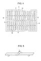
- FIG. 4 is a diagram for describing the manufacturing method for a heating resistor element component according to this embodiment, in which the process of FIG. 3B is viewed from above.
- a heating resistor element component 1 manufactured by the manufacturing method for a heating resistor element component according to this embodiment is a thermal head used in a thermal printer (hereinafter, referred to as "thermal head").
- the thermal head 1 includes a supporting substrate (hereinafter, referred to as "substrate") 2 and an undercoat (insulating film) 3 formed on the substrate 2.
- substrate a supporting substrate
- undercoat insulating film
- a plurality of heating resistors 4 are formed at intervals in one direction on the undercoat 3, and wiring 5 is connected to the heating resistors 4.
- the wiring 5 is formed of a common wire 5a connected to one end of each of the heating resistors 4 in an object-to-be-printed feeding direction (transport direction: arrangement direction), which is perpendicular to an arrangement direction of the heating resistors 4, and individual wires 5b connected to the other end thereof.
- the thermal head 1 includes a protective film 6 which covers top surfaces of the heating resistors 4 and a top surface of the wiring 5.
- heating portion a portion in which the heating resistor 4 actually generates heat (hereinafter, referred to as "heating portion") is a portion which does not overlap the wiring 5.
- a concave portion 8 which forms a hollow portion (void heat insulating layer) 7.
- the concave portion 8 is provided to form the hollow portion (void heat insulating layer) 7 for each heating resistor 4, and adjacent concave portions 8 are separated (partitioned) from each other by an inter-dot barrier 9.
- a space formed (enclosed) with a bottom surface (surface parallel to the surface of the substrate 2) and wall surfaces (surfaces perpendicular to the surface of the substrate 2) of the concave portion 8 and a rear surface (lower surface in FIG. 2 ) of the undercoat 3 forms the hollow portion 7.
- an entire surface (upper surface in FIG. 2 ) of the inter-dot barrier 9 located between the adjacent concave portions 8 abuts on the rear surface of the undercoat 3.
- the adjacent concave portions 8 are sectioned (partitioned) by the inter-dot barrier 9.
- the concave portion 8 which forms the hollow portion 7 is processed.
- a material for the substrate for example, a glass substrate or a single-crystal silicon substrate is used.
- a thickness of the substrate 2 is about 300 ⁇ m to 1 mm.
- the concave portion 8 is formed on the surface of the substrate 2 by sandblasting, dry etching, wet etching, laser processing, or the like.
- the surface of the substrate 2 is covered with a photoresist material, and the photoresist material is exposed to light using a photo mask having a predetermined pattern, thereby solidifying a portion other than a region in which the concave portions 8 are to be formed. Then, the surface of the substrate 2 is washed, and the photoresist material which has not been solidified is removed, thereby obtaining an etching mask having etching windows formed in the region in which the concave portions 8 are to be formed. The surface of the substrate 2 is subjected to sandblasting in this state, and thus the concave portion 8 having a predetermined depth is obtained.
- the etching mask having the etching windows formed in the region in which the concave portions 8 are to be formed is formed on the surface of the substrate 2 in the same manner, and the surface of the substrate 2 is subjected to etching in this state, whereby the concave portion 8 having the predetermined depth is obtained.
- wet etching is performed using an etching liquid such as a tetramethylammonium hydroxide solution, a KOH solution, a mixed liquid of fluorinated acid and nitric acid, or the like in the case of the single-crystal silicon, and wet etching is performed using a fluorinated acid etching liquid or the like in the case of the glass substrate.
- dry etching such as reactive ion etching (RIE) or plasma etching may be employed.
- a concave part 10 having a rectangular shape in plan view is processed on the surface of the substrate 2 in the arrangement direction of the concave portions 8 by the method similar to that of the concave portion 8.
- the undercoats 3 are bonded to the substrate 2.
- bonding is performed by thermal fusion bonding in which a bonding layer is not used.
- the process of bonding the undercoats 3 made of sheet glass to the substrate 2 made of glass is performed at temperature equal to or higher than annealing points of the substrate 2 made of glass and the undercoats 3 made of sheet glass and equal to or lower than softening points thereof. For this reason, shape accuracy of the substrate 2 and the undercoats 3 can be maintained, which provides high reliability.
- the undercoat 3 made of sheet glass is easily broken if a length L (mm) thereof is long (large), if a width B (mm) thereof is narrow (small), or if a plate thickness t (mm) thereof is thin (small).
- FIG. 6 is a table showing test results thereof, and in FIG. 6 , ⁇ represents a generated stress (MPa) which is obtained by an equation 3PL/2Bt 2 , judgement "o” indicates that the sheet glass is not broken, and judgement "x” indicates that the sheet glass is broken. From FIG. 6 , it is conceivable that the sheet glass is not broken when a value of ⁇ is equal to or smaller than 1,000, and that the sheet glass is broken when the value exceeds 1,000.
- MPa generated stress
- a depth h (not shown) of the concave part 10 is set to a value which is equal to or a little (slightly) smaller than the plate thickness t of the undercoat 3.
- the heating resistors 4 (see FIG. 2 ), the individual wires 5b and the common wire 5a (see FIG. 2 ), and the protective film 6 (see FIG. 2 ) are sequentially formed on the undercoat 3 thus formed. It should be noted that the heating resistors 4, the individual wires 5b, and the common wire 5a are formed in an appropriate order.
- the heating resistors 4, the individual wires 5b, the common wire 5a, and the protective film 6 can be manufactured using a manufacturing method therefor which is conventionally employed in a thermal head. Specifically, a thin film formation method such as sputtering, chemical vapor deposition (CVD), and vapor deposition is used to form a thin film made of a Ta-based or silicide-based heating resistor material on the insulating film, and the thin film made of the heating resistor material is molded using lift-off, etching, or the like, whereby a heating resistor having a desired shape is formed.
- a thin film formation method such as sputtering, chemical vapor deposition (CVD), and vapor deposition is used to form a thin film made of a Ta-based or silicide-based heating resistor material on the insulating film, and the thin film made of the heating resistor material is molded using lift-off, etching, or the like, whereby a heating resistor having a desired shape is formed.
- a film made of a wiring material such as Al, Al-Si, Au, Ag, Cu, and Pt is prepared using sputtering, vapor deposition, or the like to be formed using lift-off or etching, or the wiring material is screen-printed and is, for example, baked thereafter, to thereby form the individual wires 5b and the common wire 5a which have the desired shape.
- a film made of a protective film material such as SiO 2 , Ta 2 O 5 , SiAION, Si 3 N 4 , or diamond-like carbon is formed on the undercoat 3 using sputtering, ion plating, CVD, or the like to form the protective film 6.
- a plurality of undercoats 3 made of sheet glass are placed on one substrate 2, and the size (in particular, length L (mm) and width B (mm)) of the undercoat 3 becomes considerably smaller compared with the conventional manufacturing method in which only one undercoat 3 is placed on one substrate 2, with the result that the undercoat 3 can be handled easily. Accordingly, damage caused in the undercoat 3 during the manufacturing process can be greatly reduced, thereby reducing the manufacturing cost.
- each undercoat 3 made of sheet glass, which is smaller (for example, slightly smaller) than the concave part 10 is inserted into the concave part 10 individually, with the result that accurate alignment and temporary fixation for preventing misalignment between the substrate 2 and the undercoat 3, which are required in the conventional manufacturing method, can be made unnecessary, achieving a simplification of the manufacturing process.
- the bonding area between the substrate 2 and the undercoat 3 can be considerably reduced, and hence a spot having an adhesion failure which occurs between the undercoat 3 and the substrate 2 can be reduced.
- the undercoat 3 can be prevented from peeling off from the substrate 2 during the manufacturing process, ensuring a high yield.
- a manufacturing method for a thermal head according to a second embodiment of the present invention is described with reference to FIG. 8 .
- FIG. 8 is a view for describing the manufacturing method for a thermal head according to this embodiment, which is a plan view in which a process corresponding to the process of FIG. 3B is viewed from above.
- the manufacturing method for a thermal head according to this embodiment is different from the manufacturing method according to the first embodiment described above in that there is provided the step of forming a concave part 20 having a rectangular shape in plan view (oblong shape in this embodiment) on the surface of the substrate 2 in the arrangement direction of the concave portions 8 for each region straddling a plurality of (52 in this embodiment) concave portions 8, which correspond to four products.
- Other respects are the same as those of the first embodiment described above, and hence their descriptions are omitted here.
- the manufacturing method for a thermal head of this embodiment the number of the undercoats 3 made of sheet glass becomes fewer than that of the first embodiment (becomes a quarter of the number of the first embodiment), and hence the number of placing the undercoat 3 on the substrate 2 becomes fewer (becomes a quarter of the number of the first embodiment). Therefore, the manufacturing process can be simplified.
- a manufacturing method for a thermal head according to a third embodiment of the present invention is described with reference to FIG. 9 .
- FIG. 9 is a view for describing the manufacturing method for a thermal head according to this embodiment, which is a plan view in which a process corresponding to the process of FIG. 3B is viewed from above.
- the manufacturing method for a thermal head according to this embodiment is different from the manufacturing method according to the first embodiment described above in that there is provided the step of forming a concave part 30 having a rectangular shape in plan view (oblong shape in this embodiment) on the surface of the substrate 2 in the arrangement direction and a transport direction (direction orthogonal to the arrangement direction) of the concave portions 8 for each region straddling a plurality of (104 in this embodiment) concave portions 8, which correspond to eight products.
- Other respects are the same as those of the first embodiment described above, and hence their descriptions are omitted here.
- the manufacturing method for a thermal head of this embodiment the number of the undercoats 3 made of sheet glass becomes fewer than that of the first embodiment (becomes one eighth of the number of the first embodiment), and hence the number of placing the undercoat 3 on the substrate 2 becomes fewer (becomes one eighth of the number of the first embodiment). Therefore, the manufacturing process can be simplified.
- the manufacturing method for a thermal head according to the present invention is not limited to those of the embodiments described above, and they can be modified, changed, and combined as appropriate according to the necessity.
- the descriptions are made of the case where the concave portions 8 are formed on the surface of the substrate 2, and then, the concave parts 10, 20, or 30 are formed.
- the concave portions 8 may be formed after the formation of the concave parts 10, 20, or 30.
- the numbers of concave portions 8 in each product and the number of products in each concave part 10, 20, 30 can be selected as appropriate.
Landscapes
- Engineering & Computer Science (AREA)
- Manufacturing & Machinery (AREA)
- Electronic Switches (AREA)
- Apparatuses And Processes For Manufacturing Resistors (AREA)
- Surface Heating Bodies (AREA)
Abstract
Description
- The present invention relates to a manufacturing method for a heating resistor element component (thermal head) which is used in a thermal printer typically mounted onto a compact information equipment terminal such as a compact handy terminal, and performs printing on a thermal recording medium through selective driving of a plurality of heating elements based on print data.
- Recently, thermal printers have been widely used in compact information equipment terminals. The compact information equipment terminals are driven by a battery, which leads to strong demands for electric power saving of the thermal printers. Accordingly, there have been growing demands for thermal heads having high heating efficiency.
- As to increasing efficiency of the thermal head, there is known a method of forming a heat insulating layer in a lower layer of a heating resistor (for example, see Patent Document
JP 2007-83532 A - In the case where the thermal head as described above is manufactured, one undercoat is placed on one substrate. Accordingly, a size (in particular, length and width) of the undercoat is increased, and the thus manufactured thermal head is difficult to be handled, leading to a fear that the undercoat may be damaged during transportation.
- In addition, a bonding area between the substrate and the undercoat is increased, which leads to a fear that a spot having an adhesion failure is generated between the undercoat and the substrate, the undercoat peels off from the substrate during manufacturing process, and a yield is reduced.
- The present invention has been made in view of the above-mentioned circumstances, and an object thereof is to provide a manufacturing method for a heating resistor element component, which is capable of facilitating handling of the undercoat, reducing damage of the undercoat, and ensuring a high yield.
- In order to solve the aforementioned problems, the present invention employs the following means.
- According to the present invention, a manufacturing method for a heating resistor element component includes the steps of: processing, on a surface of a supporting substrate, a plurality of concave portions each forming a hollow portion at intervals; processing, on the surface of the supporting substrate, a concave part for each region straddling the plurality of concave portions in an arrangement direction of the concave portions; placing an insulating film made of sheet glass in each concave part; and bonding the insulating film to the supporting substrate.
- According to the manufacturing method for a heating resistor element component of the present invention, a plurality of the insulating films made of sheet glass are placed on one supporting substrate, and a size (in particular, length L (mm) and width B (mm)) of the insulating film becomes smaller compared with a conventional manufacturing method in which only one insulating film is placed on one supporting substrate, whereby the insulating film can be easily handled and damage caused in the insulating film during the manufacturing process can be reduced. Accordingly, manufacturing cost can be reduced.
- In addition, compared with the conventional manufacturing method in which the insulating film is formed over the entire surface of the supporting substrate, the bonding area between the supporting substrate and the insulating film can be greatly reduced, and hence a spot having an adhesion failure which occurs between the insulating film and the supporting substrate can be reduced. As a result, the insulating film can be prevented from peeling off from the supporting substrate during the manufacturing process, which ensures a high yield.
- In the manufacturing method for a heating resistor element component, it is more preferable that the size of the insulating film be set by performing a three-point bend test through application of a load P of 0.1 (N) to a center portion in a longitudinal direction of the insulating film having the length L (mm), the width B (mm), and a plate thickness t (mm) so that a generated stress σ (MPa) obtained by an equation 3PL/2Bt2 is equal to or smaller than 1,000.
- According to the manufacturing method for a heating resistor element component as described above, a strength of the insulating film itself is ensured, and the insulating film itself is resistant to damage (is hard to break), which further facilitates handling of the insulating film. Accordingly, the damage caused in the insulating film during manufacturing process can be further reduced, to thereby reduce a manufacturing cost.
- In the heating resistor element component, it is more preferable that a length EL (mm) of the concave part and a width EB (mm) of the concave part be set so that a value obtained by subtracting the length L (mm) of the insulating film from the length EL (mm) of the concave part and a value obtained by subtracting the width B (mm) of the insulating film from the width EB (mm) of the concave part are each 0.1 to 0.4 (mm).
- According to the manufacturing method for a heating resistor element component as described above, the insulating film made of sheet glass, which is smaller than the concave part (for example, is slightly smaller), is inserted into each concave part one by one, which eliminates the necessity for accurate alignment and temporary fixation for preventing misalignment between the supporting substrate and the insulating film, which are required in the conventional manufacturing method. Therefore, the manufacturing process can be simplified.
- According to the present invention, there are achieved effects that handling of the insulating film can be facilitated, damage of the insulating film can be reduced, and a high yield can be ensured.
- Embodiments of the present invention will now be described by way of further example only and with reference to the accompanying drawings, in which:
-
FIG. 1 is a plan view of a heating resistor element component manufactured by a manufacturing method for a heating resistor element component according to a first embodiment of the present invention, which illustrates a state in which a protective film is removed; -
FIG. 2 is a cross-sectional view taken along an arrow II-II ofFIG. 1 ; -
FIGS. 3A-3C are process drawings for describing the manufacturing method for a heating resistor element component according to the first embodiment of the present invention; -
FIG. 4 is a diagram for describing the manufacturing method for a heating resistor element component according to the first embodiment of the present invention, in which a process ofFIG. 3B is viewed from above; -
FIG. 5 is a conceptual diagram of a three-point bend test; -
FIG. 6 is a table showing test results of the three-point bend test, in which a load P of 0.1 (N) is applied to a center portion in a longitudinal direction of a sheet glass having a certain size (length L (mm), width B (mm), and plate thickness t (mm)), as to whether or not the sheet glass is broken; -
FIG. 7 is a plan view in which a process ofFIG. 3C is viewed from above, which is an enlarged view of a pair of a concave portion and an undercoat; -
FIG. 8 is a view for describing a manufacturing method for a heating resistor element component according to a second embodiment of the present invention, which is a plan view in which a process corresponding to the process ofFIG. 3B is viewed from above; and -
FIG. 9 is a view for describing a manufacturing method for a heating resistor element component according to a third embodiment of the present invention, which is a plan view in which the process corresponding to the process ofFIG. 3B is viewed from above. - Hereinafter, with reference to
FIG. 1 to FIG. 4 , a manufacturing method for a heating resistor element component according to a first embodiment of the present invention is described. -
FIG. 1 is a plan view of a thermal head which is a heating resistor element component manufactured by the manufacturing method for a heating resistor element component according to this embodiment, which illustrates a state in which a protective film is removed.FIG. 2 is a cross-sectional view taken along the line II-II ofFIG. 1 .FIGS. 3A -3C are process drawings for describing the manufacturing method for a heating resistor element component according to this embodiment.FIG. 4 is a diagram for describing the manufacturing method for a heating resistor element component according to this embodiment, in which the process ofFIG. 3B is viewed from above. - A heating
resistor element component 1 manufactured by the manufacturing method for a heating resistor element component according to this embodiment is a thermal head used in a thermal printer (hereinafter, referred to as "thermal head"). - As illustrated in
FIG. 2 , thethermal head 1 includes a supporting substrate (hereinafter, referred to as "substrate") 2 and an undercoat (insulating film) 3 formed on thesubstrate 2. In addition, as illustrated inFIG. 1 andFIG. 2 , a plurality ofheating resistors 4 are formed at intervals in one direction on theundercoat 3, andwiring 5 is connected to theheating resistors 4. Thewiring 5 is formed of acommon wire 5a connected to one end of each of theheating resistors 4 in an object-to-be-printed feeding direction (transport direction: arrangement direction), which is perpendicular to an arrangement direction of theheating resistors 4, andindividual wires 5b connected to the other end thereof. Further, as illustrated inFIG. 2 , thethermal head 1 includes aprotective film 6 which covers top surfaces of theheating resistors 4 and a top surface of thewiring 5. - It should be noted that a portion in which the
heating resistor 4 actually generates heat (hereinafter, referred to as "heating portion") is a portion which does not overlap thewiring 5. - As illustrated in
FIG. 1 andFIG. 2 , on a surface (upper surface inFIG. 2 ) of thesubstrate 2, there is formed aconcave portion 8 which forms a hollow portion (void heat insulating layer) 7. - The
concave portion 8 is provided to form the hollow portion (void heat insulating layer) 7 for eachheating resistor 4, and adjacentconcave portions 8 are separated (partitioned) from each other by aninter-dot barrier 9. A space formed (enclosed) with a bottom surface (surface parallel to the surface of the substrate 2) and wall surfaces (surfaces perpendicular to the surface of the substrate 2) of theconcave portion 8 and a rear surface (lower surface inFIG. 2 ) of theundercoat 3 forms thehollow portion 7. - Through the formation of the plurality of
concave portions 8 on the surface of thesubstrate 2, an entire surface (upper surface inFIG. 2 ) of theinter-dot barrier 9 located between the adjacentconcave portions 8 abuts on the rear surface of theundercoat 3. In other words, the adjacentconcave portions 8 are sectioned (partitioned) by theinter-dot barrier 9. - Next, with reference to
FIGS. 3A-3C andFIG. 4 , a manufacturing method for thethermal head 1 according to this embodiment is described. - First, as illustrated in
FIG. 3A , for each region on the surface of thesubstrate 2 having a uniform thickness, in which theheating resistors 4 are formed, theconcave portion 8 which forms thehollow portion 7 is processed. As a material for thesubstrate 2, for example, a glass substrate or a single-crystal silicon substrate is used. A thickness of thesubstrate 2 is about 300 µm to 1 mm. - The
concave portion 8 is formed on the surface of thesubstrate 2 by sandblasting, dry etching, wet etching, laser processing, or the like. - In the case where the
substrate 2 is processed by sandblasting, the surface of thesubstrate 2 is covered with a photoresist material, and the photoresist material is exposed to light using a photo mask having a predetermined pattern, thereby solidifying a portion other than a region in which theconcave portions 8 are to be formed. Then, the surface of thesubstrate 2 is washed, and the photoresist material which has not been solidified is removed, thereby obtaining an etching mask having etching windows formed in the region in which theconcave portions 8 are to be formed. The surface of thesubstrate 2 is subjected to sandblasting in this state, and thus theconcave portion 8 having a predetermined depth is obtained. - In the case where processing is performed through etching, the etching mask having the etching windows formed in the region in which the
concave portions 8 are to be formed is formed on the surface of thesubstrate 2 in the same manner, and the surface of thesubstrate 2 is subjected to etching in this state, whereby theconcave portion 8 having the predetermined depth is obtained. In the etching process, for example, wet etching is performed using an etching liquid such as a tetramethylammonium hydroxide solution, a KOH solution, a mixed liquid of fluorinated acid and nitric acid, or the like in the case of the single-crystal silicon, and wet etching is performed using a fluorinated acid etching liquid or the like in the case of the glass substrate. In addition, dry etching such as reactive ion etching (RIE) or plasma etching may be employed. - Next, the etching mask is all removed from the surface of the
substrate 2. Then, as illustrated inFIG. 3B andFIG. 4 , for each region straddling the plurality of (13 in this embodiment)concave portions 8, which correspond to one product, aconcave part 10 having a rectangular shape in plan view (oblong shape in this embodiment) is processed on the surface of thesubstrate 2 in the arrangement direction of theconcave portions 8 by the method similar to that of theconcave portion 8. - Then, the
undercoat 3 made of sheet glass, which is smaller (for example, slightly smaller) than theconcave part 10, is placed (is inserted) in eachconcave part 10 one by one. When theundercoats 3 have been put in all theconcave parts 10, theundercoats 3 are bonded to thesubstrate 2. - It should be noted that, in the case where the
undercoats 3 made of sheet glass are bonded to thesubstrate 2 made of glass, bonding is performed by thermal fusion bonding in which a bonding layer is not used. The process of bonding theundercoats 3 made of sheet glass to thesubstrate 2 made of glass is performed at temperature equal to or higher than annealing points of thesubstrate 2 made of glass and theundercoats 3 made of sheet glass and equal to or lower than softening points thereof. For this reason, shape accuracy of thesubstrate 2 and theundercoats 3 can be maintained, which provides high reliability. - The
undercoat 3 made of sheet glass is easily broken if a length L (mm) thereof is long (large), if a width B (mm) thereof is narrow (small), or if a plate thickness t (mm) thereof is thin (small). - Here, by the method as illustrated in
FIG. 5 , a load P of 0.1 (N) is applied to a center portion in a longitudinal direction of the sheet glass having a certain size (length L (mm), width B (mm), and plate thickness t (mm)), and there is performed a three-point bend test as to whether or not the sheet glass is broken.FIG. 6 is a table showing test results thereof, and inFIG. 6 , σ represents a generated stress (MPa) which is obtained by an equation 3PL/2Bt2, judgement "o" indicates that the sheet glass is not broken, and judgement "x" indicates that the sheet glass is broken. FromFIG. 6 , it is conceivable that the sheet glass is not broken when a value of σ is equal to or smaller than 1,000, and that the sheet glass is broken when the value exceeds 1,000. - Therefore, as the size of the
undercoat 3 placed (inserted) in theconcave part 10, a condition of σ≤1,000 (more preferably, condition of σ≤500) needs to be satisfied. - On the other hand, a length EL (mm) and a width EB (mm) of the
concave part 10, which are illustrated inFIG. 7 , are set to EL-L=0.1 to 0.4 (mm) and EB-B=0.1 to 0.4 (mm), respectively. A depth h (not shown) of theconcave part 10 is set to a value which is equal to or a little (slightly) smaller than the plate thickness t of theundercoat 3. - It should be noted that, if EL-L=0.1 (mm) and EB-B=0.1 (mm), the
undercoat 3 is completely inserted into theconcave part 10 without rattling, and if 0.1 (mm)<EL-L≤0.4 (mm) and 0.1 (mm)<EB-B≤0.4 (mm), manufacturing can be performed without any difficulty while there is a little rattling (gap) therebetween. - Next, the heating resistors 4 (see
FIG. 2 ), theindividual wires 5b and thecommon wire 5a (seeFIG. 2 ), and the protective film 6 (seeFIG. 2 ) are sequentially formed on theundercoat 3 thus formed. It should be noted that theheating resistors 4, theindividual wires 5b, and thecommon wire 5a are formed in an appropriate order. - The
heating resistors 4, theindividual wires 5b, thecommon wire 5a, and theprotective film 6 can be manufactured using a manufacturing method therefor which is conventionally employed in a thermal head. Specifically, a thin film formation method such as sputtering, chemical vapor deposition (CVD), and vapor deposition is used to form a thin film made of a Ta-based or silicide-based heating resistor material on the insulating film, and the thin film made of the heating resistor material is molded using lift-off, etching, or the like, whereby a heating resistor having a desired shape is formed. - Similarly, on the
undercoat 3, a film made of a wiring material such as Al, Al-Si, Au, Ag, Cu, and Pt is prepared using sputtering, vapor deposition, or the like to be formed using lift-off or etching, or the wiring material is screen-printed and is, for example, baked thereafter, to thereby form theindividual wires 5b and thecommon wire 5a which have the desired shape. - After the formation of the
heating resistors 4, theindividual wires 5b, and thecommon wire 5a as described above, a film made of a protective film material such as SiO2, Ta2O5, SiAION, Si3N4, or diamond-like carbon is formed on theundercoat 3 using sputtering, ion plating, CVD, or the like to form theprotective film 6. - According to the manufacturing method for the
thermal head 1 of this embodiment, a plurality ofundercoats 3 made of sheet glass are placed on onesubstrate 2, and the size (in particular, length L (mm) and width B (mm)) of theundercoat 3 becomes considerably smaller compared with the conventional manufacturing method in which only oneundercoat 3 is placed on onesubstrate 2, with the result that theundercoat 3 can be handled easily. Accordingly, damage caused in theundercoat 3 during the manufacturing process can be greatly reduced, thereby reducing the manufacturing cost. - Moreover, according to the manufacturing method for the
thermal head 1 of this embodiment, eachundercoat 3 made of sheet glass, which is smaller (for example, slightly smaller) than theconcave part 10, is inserted into theconcave part 10 individually, with the result that accurate alignment and temporary fixation for preventing misalignment between thesubstrate 2 and theundercoat 3, which are required in the conventional manufacturing method, can be made unnecessary, achieving a simplification of the manufacturing process. - Further, according to the manufacturing method for the
thermal head 1 of this embodiment, compared with the conventional manufacturing method in which theundercoat 3 is formed on the entire surface of thesubstrate 2, the bonding area between thesubstrate 2 and theundercoat 3 can be considerably reduced, and hence a spot having an adhesion failure which occurs between theundercoat 3 and thesubstrate 2 can be reduced. As a result, theundercoat 3 can be prevented from peeling off from thesubstrate 2 during the manufacturing process, ensuring a high yield. - A manufacturing method for a thermal head according to a second embodiment of the present invention is described with reference to
FIG. 8 . -
FIG. 8 is a view for describing the manufacturing method for a thermal head according to this embodiment, which is a plan view in which a process corresponding to the process ofFIG. 3B is viewed from above. - As illustrated in
FIG. 8 , the manufacturing method for a thermal head according to this embodiment is different from the manufacturing method according to the first embodiment described above in that there is provided the step of forming aconcave part 20 having a rectangular shape in plan view (oblong shape in this embodiment) on the surface of thesubstrate 2 in the arrangement direction of theconcave portions 8 for each region straddling a plurality of (52 in this embodiment)concave portions 8, which correspond to four products. Other respects are the same as those of the first embodiment described above, and hence their descriptions are omitted here. - According to the manufacturing method for a thermal head of this embodiment, the number of the
undercoats 3 made of sheet glass becomes fewer than that of the first embodiment (becomes a quarter of the number of the first embodiment), and hence the number of placing theundercoat 3 on thesubstrate 2 becomes fewer (becomes a quarter of the number of the first embodiment). Therefore, the manufacturing process can be simplified. - Other operation and effect are the same as those of the first embodiment described above, and hence their descriptions are omitted here.
- A manufacturing method for a thermal head according to a third embodiment of the present invention is described with reference to
FIG. 9 . -
FIG. 9 is a view for describing the manufacturing method for a thermal head according to this embodiment, which is a plan view in which a process corresponding to the process ofFIG. 3B is viewed from above. - As illustrated in
FIG. 9 , the manufacturing method for a thermal head according to this embodiment is different from the manufacturing method according to the first embodiment described above in that there is provided the step of forming aconcave part 30 having a rectangular shape in plan view (oblong shape in this embodiment) on the surface of thesubstrate 2 in the arrangement direction and a transport direction (direction orthogonal to the arrangement direction) of theconcave portions 8 for each region straddling a plurality of (104 in this embodiment)concave portions 8, which correspond to eight products. Other respects are the same as those of the first embodiment described above, and hence their descriptions are omitted here. - According to the manufacturing method for a thermal head of this embodiment, the number of the
undercoats 3 made of sheet glass becomes fewer than that of the first embodiment (becomes one eighth of the number of the first embodiment), and hence the number of placing theundercoat 3 on thesubstrate 2 becomes fewer (becomes one eighth of the number of the first embodiment). Therefore, the manufacturing process can be simplified. - Other operation and effect are the same as those of the first embodiment described above, and hence their descriptions are omitted here.
- The manufacturing method for a thermal head according to the present invention is not limited to those of the embodiments described above, and they can be modified, changed, and combined as appropriate according to the necessity.
- For example, in the embodiments described above, the descriptions are made of the case where the
concave portions 8 are formed on the surface of thesubstrate 2, and then, theconcave parts concave portions 8 may be formed after the formation of theconcave parts - In addition, the numbers of
concave portions 8 in each product and the number of products in eachconcave part - The foregoing description has been given by way of example only and it will be appreciated by a person skilled in the art that modifications can be made without departing from the scope of the present invention.
Claims (3)
- A manufacturing method for a heating resistor element component (1), comprising the steps of:processing, on a surface of a supporting substrate (2), a plurality of concave portions (8) each forming a hollow portion (7) at intervals;processing, on the surface of the supporting substrate, a concave part (10, 20, 30) for each region straddling the plurality of concave portions in an arrangement direction of the concave portions;placing an insulating film (3) made of sheet glass in each concave part; andbonding the insulating film to the supporting substrate.
- A manufacturing method for a heating resistor element component according to claim 1, wherein a size of the insulating film (3) is set by performing a three-point bend test through application of a load P of 0.1 (N) to a center portion in a longitudinal direction of the insulating film having a length L (mm), a width B (mm), and a plate thickness t (mm) so that a generated stress σ (MPa) obtained by an equation 3PL/2Bt2 is equal to or smaller than 1,000.
- A manufacturing method for a heating resistor element component according to claim 2, wherein a length EL (mm) of the concave part and a width EB (mm) of the concave part are set so that a value obtained by subtracting the length L (mm) of the insulating film from the length EL (mm) of the concave part and a value obtained by subtracting the width B (mm) of the insulating film from the width EB (mm) of the concave part are each 0.1 to 0.4 (mm).
Applications Claiming Priority (1)
| Application Number | Priority Date | Filing Date | Title |
|---|---|---|---|
| JP2008115752A JP5181152B2 (en) | 2008-04-25 | 2008-04-25 | Manufacturing method of thermal head |
Publications (3)
| Publication Number | Publication Date |
|---|---|
| EP2111993A2 true EP2111993A2 (en) | 2009-10-28 |
| EP2111993A3 EP2111993A3 (en) | 2010-10-27 |
| EP2111993B1 EP2111993B1 (en) | 2012-05-16 |
Family
ID=40873512
Family Applications (1)
| Application Number | Title | Priority Date | Filing Date |
|---|---|---|---|
| EP09158249A Not-in-force EP2111993B1 (en) | 2008-04-25 | 2009-04-20 | Manufacturing method for a heating resistor element component |
Country Status (3)
| Country | Link |
|---|---|
| US (1) | US8122591B2 (en) |
| EP (1) | EP2111993B1 (en) |
| JP (1) | JP5181152B2 (en) |
Families Citing this family (4)
| Publication number | Priority date | Publication date | Assignee | Title |
|---|---|---|---|---|
| JP5424386B2 (en) * | 2009-07-29 | 2014-02-26 | セイコーインスツル株式会社 | Thermal head and printer |
| JP5424387B2 (en) * | 2009-08-06 | 2014-02-26 | セイコーインスツル株式会社 | Thermal head and method for manufacturing thermal head |
| JP5541660B2 (en) * | 2009-08-06 | 2014-07-09 | セイコーインスツル株式会社 | Manufacturing method of thermal head |
| JP5943414B2 (en) * | 2011-12-01 | 2016-07-05 | セイコーインスツル株式会社 | Manufacturing method of thermal head |
Citations (1)
| Publication number | Priority date | Publication date | Assignee | Title |
|---|---|---|---|---|
| JP2007083532A (en) | 2005-09-22 | 2007-04-05 | Seiko Instruments Inc | Heating resistance element, thermal head, printer, and method of manufacturing heating resistance element |
Family Cites Families (9)
| Publication number | Priority date | Publication date | Assignee | Title |
|---|---|---|---|---|
| JPS63249664A (en) * | 1987-04-06 | 1988-10-17 | Oki Electric Ind Co Ltd | Substrate for thermal head and manufacture thereof |
| JP2583965B2 (en) * | 1988-05-20 | 1997-02-19 | 松下電器産業株式会社 | Thermal head |
| US5204282A (en) * | 1988-09-30 | 1993-04-20 | Nippon Soken, Inc. | Semiconductor circuit structure and method for making the same |
| JPH03218856A (en) * | 1989-11-20 | 1991-09-26 | Ricoh Co Ltd | thermal head |
| JPH0848050A (en) * | 1994-05-31 | 1996-02-20 | Rohm Co Ltd | Thermal print head |
| CN1086639C (en) * | 1994-05-31 | 2002-06-26 | 罗姆股份有限公司 | Thermal printing head, substrate used thereof and method for producing the substrate |
| JPH08310024A (en) * | 1995-05-17 | 1996-11-26 | Rohm Co Ltd | Thin film type thermal print head and method of manufacturing the same |
| JP2002370396A (en) * | 2001-06-13 | 2002-12-24 | Sii P & S Inc | Thermal head unit and method of manufacturing the same |
| JP2003054020A (en) * | 2001-08-09 | 2003-02-26 | Alps Electric Co Ltd | Thermal head and manufacturing method thereof |
-
2008
- 2008-04-25 JP JP2008115752A patent/JP5181152B2/en not_active Expired - Fee Related
-
2009
- 2009-04-20 EP EP09158249A patent/EP2111993B1/en not_active Not-in-force
- 2009-04-23 US US12/386,843 patent/US8122591B2/en not_active Expired - Fee Related
Patent Citations (1)
| Publication number | Priority date | Publication date | Assignee | Title |
|---|---|---|---|---|
| JP2007083532A (en) | 2005-09-22 | 2007-04-05 | Seiko Instruments Inc | Heating resistance element, thermal head, printer, and method of manufacturing heating resistance element |
Also Published As
| Publication number | Publication date |
|---|---|
| EP2111993A3 (en) | 2010-10-27 |
| JP5181152B2 (en) | 2013-04-10 |
| EP2111993B1 (en) | 2012-05-16 |
| JP2009262439A (en) | 2009-11-12 |
| US20090265919A1 (en) | 2009-10-29 |
| US8122591B2 (en) | 2012-02-28 |
Similar Documents
| Publication | Publication Date | Title |
|---|---|---|
| EP2111993B1 (en) | Manufacturing method for a heating resistor element component | |
| US8415589B2 (en) | Heating resistance element component and thermal printer | |
| US8256099B2 (en) | Manufacturing method for a thermal head | |
| EP2298562B1 (en) | Thermal head and printer | |
| EP2281692B1 (en) | Thermal head and manufacturing method for the thermal head | |
| KR100910679B1 (en) | Thermal print head and its manufacturing method | |
| US7852361B2 (en) | Heating resistance element component and printer | |
| EP2327554B1 (en) | Thermal head, manufacturing method therefor, and printer | |
| US8621888B2 (en) | Manufacturing method for a thermal head | |
| EP2052867A1 (en) | Thermal print head | |
| US7956880B2 (en) | Heating resistor element component, thermal printer, and manufacturing method for a heating resistor element component | |
| US12077005B2 (en) | Thermal print head, thermal printer, and method for manufacturing thermal print head | |
| JP5200230B2 (en) | Heating resistance element parts and thermal printer | |
| EP1043165A1 (en) | Thermal print head and method of manufacturing the same | |
| CN101193753A (en) | Thermal print head and manufacturing method thereof | |
| EP2492101B1 (en) | Thermal Head and Method of Manufacturing the same, and Printer | |
| JPWO1996041722A1 (en) | Method for forming auxiliary electrode layer for common electrode pattern in thermal head | |
| US20120073123A1 (en) | Method of manufacturing thermal head | |
| JP5181328B2 (en) | Heating resistance element parts and thermal printer | |
| US6330014B1 (en) | Thermal head manufactured by sequentially laminating conductive layer, layer insulating layer and heater element on heat insulating layer | |
| US20120224015A1 (en) | Thermal head and method of manufacturing the same | |
| JP7701181B2 (en) | Thermal printhead, its manufacturing method, and thermal printer | |
| JPH03222760A (en) | Thermal head and manufacture thereof | |
| KR20070087767A (en) | Heaters for inkjet printheads and inkjet printheads having the heaters | |
| JP3471872B2 (en) | Thermal print head |
Legal Events
| Date | Code | Title | Description |
|---|---|---|---|
| PUAI | Public reference made under article 153(3) epc to a published international application that has entered the european phase |
Free format text: ORIGINAL CODE: 0009012 |
|
| AK | Designated contracting states |
Kind code of ref document: A2 Designated state(s): AT BE BG CH CY CZ DE DK EE ES FI FR GB GR HR HU IE IS IT LI LT LU LV MC MK MT NL NO PL PT RO SE SI SK TR |
|
| PUAL | Search report despatched |
Free format text: ORIGINAL CODE: 0009013 |
|
| AK | Designated contracting states |
Kind code of ref document: A3 Designated state(s): AT BE BG CH CY CZ DE DK EE ES FI FR GB GR HR HU IE IS IT LI LT LU LV MC MK MT NL NO PL PT RO SE SI SK TR |
|
| 17P | Request for examination filed |
Effective date: 20110107 |
|
| GRAP | Despatch of communication of intention to grant a patent |
Free format text: ORIGINAL CODE: EPIDOSNIGR1 |
|
| GRAS | Grant fee paid |
Free format text: ORIGINAL CODE: EPIDOSNIGR3 |
|
| GRAA | (expected) grant |
Free format text: ORIGINAL CODE: 0009210 |
|
| AK | Designated contracting states |
Kind code of ref document: B1 Designated state(s): AT BE BG CH CY CZ DE DK EE ES FI FR GB GR HR HU IE IS IT LI LT LU LV MC MK MT NL NO PL PT RO SE SI SK TR |
|
| REG | Reference to a national code |
Ref country code: GB Ref legal event code: FG4D |
|
| REG | Reference to a national code |
Ref country code: CH Ref legal event code: EP |
|
| REG | Reference to a national code |
Ref country code: AT Ref legal event code: REF Ref document number: 557890 Country of ref document: AT Kind code of ref document: T Effective date: 20120615 |
|
| REG | Reference to a national code |
Ref country code: IE Ref legal event code: FG4D |
|
| REG | Reference to a national code |
Ref country code: DE Ref legal event code: R096 Ref document number: 602009006951 Country of ref document: DE Effective date: 20120726 |
|
| REG | Reference to a national code |
Ref country code: NL Ref legal event code: VDEP Effective date: 20120516 |
|
| REG | Reference to a national code |
Ref country code: LT Ref legal event code: MG4D Effective date: 20120516 |
|
| PG25 | Lapsed in a contracting state [announced via postgrant information from national office to epo] |
Ref country code: IS Free format text: LAPSE BECAUSE OF FAILURE TO SUBMIT A TRANSLATION OF THE DESCRIPTION OR TO PAY THE FEE WITHIN THE PRESCRIBED TIME-LIMIT Effective date: 20120916 Ref country code: LT Free format text: LAPSE BECAUSE OF FAILURE TO SUBMIT A TRANSLATION OF THE DESCRIPTION OR TO PAY THE FEE WITHIN THE PRESCRIBED TIME-LIMIT Effective date: 20120516 Ref country code: PL Free format text: LAPSE BECAUSE OF FAILURE TO SUBMIT A TRANSLATION OF THE DESCRIPTION OR TO PAY THE FEE WITHIN THE PRESCRIBED TIME-LIMIT Effective date: 20120516 Ref country code: CY Free format text: LAPSE BECAUSE OF FAILURE TO SUBMIT A TRANSLATION OF THE DESCRIPTION OR TO PAY THE FEE WITHIN THE PRESCRIBED TIME-LIMIT Effective date: 20120516 Ref country code: NO Free format text: LAPSE BECAUSE OF FAILURE TO SUBMIT A TRANSLATION OF THE DESCRIPTION OR TO PAY THE FEE WITHIN THE PRESCRIBED TIME-LIMIT Effective date: 20120816 Ref country code: SE Free format text: LAPSE BECAUSE OF FAILURE TO SUBMIT A TRANSLATION OF THE DESCRIPTION OR TO PAY THE FEE WITHIN THE PRESCRIBED TIME-LIMIT Effective date: 20120516 Ref country code: FI Free format text: LAPSE BECAUSE OF FAILURE TO SUBMIT A TRANSLATION OF THE DESCRIPTION OR TO PAY THE FEE WITHIN THE PRESCRIBED TIME-LIMIT Effective date: 20120516 |
|
| REG | Reference to a national code |
Ref country code: AT Ref legal event code: MK05 Ref document number: 557890 Country of ref document: AT Kind code of ref document: T Effective date: 20120516 |
|
| PG25 | Lapsed in a contracting state [announced via postgrant information from national office to epo] |
Ref country code: GR Free format text: LAPSE BECAUSE OF FAILURE TO SUBMIT A TRANSLATION OF THE DESCRIPTION OR TO PAY THE FEE WITHIN THE PRESCRIBED TIME-LIMIT Effective date: 20120817 Ref country code: LV Free format text: LAPSE BECAUSE OF FAILURE TO SUBMIT A TRANSLATION OF THE DESCRIPTION OR TO PAY THE FEE WITHIN THE PRESCRIBED TIME-LIMIT Effective date: 20120516 Ref country code: PT Free format text: LAPSE BECAUSE OF FAILURE TO SUBMIT A TRANSLATION OF THE DESCRIPTION OR TO PAY THE FEE WITHIN THE PRESCRIBED TIME-LIMIT Effective date: 20120917 Ref country code: HR Free format text: LAPSE BECAUSE OF FAILURE TO SUBMIT A TRANSLATION OF THE DESCRIPTION OR TO PAY THE FEE WITHIN THE PRESCRIBED TIME-LIMIT Effective date: 20120516 Ref country code: SI Free format text: LAPSE BECAUSE OF FAILURE TO SUBMIT A TRANSLATION OF THE DESCRIPTION OR TO PAY THE FEE WITHIN THE PRESCRIBED TIME-LIMIT Effective date: 20120516 |
|
| PG25 | Lapsed in a contracting state [announced via postgrant information from national office to epo] |
Ref country code: BE Free format text: LAPSE BECAUSE OF FAILURE TO SUBMIT A TRANSLATION OF THE DESCRIPTION OR TO PAY THE FEE WITHIN THE PRESCRIBED TIME-LIMIT Effective date: 20120516 |
|
| PG25 | Lapsed in a contracting state [announced via postgrant information from national office to epo] |
Ref country code: NL Free format text: LAPSE BECAUSE OF FAILURE TO SUBMIT A TRANSLATION OF THE DESCRIPTION OR TO PAY THE FEE WITHIN THE PRESCRIBED TIME-LIMIT Effective date: 20120516 Ref country code: RO Free format text: LAPSE BECAUSE OF FAILURE TO SUBMIT A TRANSLATION OF THE DESCRIPTION OR TO PAY THE FEE WITHIN THE PRESCRIBED TIME-LIMIT Effective date: 20120516 Ref country code: CZ Free format text: LAPSE BECAUSE OF FAILURE TO SUBMIT A TRANSLATION OF THE DESCRIPTION OR TO PAY THE FEE WITHIN THE PRESCRIBED TIME-LIMIT Effective date: 20120516 Ref country code: EE Free format text: LAPSE BECAUSE OF FAILURE TO SUBMIT A TRANSLATION OF THE DESCRIPTION OR TO PAY THE FEE WITHIN THE PRESCRIBED TIME-LIMIT Effective date: 20120516 Ref country code: AT Free format text: LAPSE BECAUSE OF FAILURE TO SUBMIT A TRANSLATION OF THE DESCRIPTION OR TO PAY THE FEE WITHIN THE PRESCRIBED TIME-LIMIT Effective date: 20120516 Ref country code: DK Free format text: LAPSE BECAUSE OF FAILURE TO SUBMIT A TRANSLATION OF THE DESCRIPTION OR TO PAY THE FEE WITHIN THE PRESCRIBED TIME-LIMIT Effective date: 20120516 Ref country code: SK Free format text: LAPSE BECAUSE OF FAILURE TO SUBMIT A TRANSLATION OF THE DESCRIPTION OR TO PAY THE FEE WITHIN THE PRESCRIBED TIME-LIMIT Effective date: 20120516 |
|
| PLBE | No opposition filed within time limit |
Free format text: ORIGINAL CODE: 0009261 |
|
| STAA | Information on the status of an ep patent application or granted ep patent |
Free format text: STATUS: NO OPPOSITION FILED WITHIN TIME LIMIT |
|
| 26N | No opposition filed |
Effective date: 20130219 |
|
| PG25 | Lapsed in a contracting state [announced via postgrant information from national office to epo] |
Ref country code: ES Free format text: LAPSE BECAUSE OF FAILURE TO SUBMIT A TRANSLATION OF THE DESCRIPTION OR TO PAY THE FEE WITHIN THE PRESCRIBED TIME-LIMIT Effective date: 20120827 |
|
| REG | Reference to a national code |
Ref country code: DE Ref legal event code: R097 Ref document number: 602009006951 Country of ref document: DE Effective date: 20130219 |
|
| PG25 | Lapsed in a contracting state [announced via postgrant information from national office to epo] |
Ref country code: BG Free format text: LAPSE BECAUSE OF FAILURE TO SUBMIT A TRANSLATION OF THE DESCRIPTION OR TO PAY THE FEE WITHIN THE PRESCRIBED TIME-LIMIT Effective date: 20120816 |
|
| PG25 | Lapsed in a contracting state [announced via postgrant information from national office to epo] |
Ref country code: MC Free format text: LAPSE BECAUSE OF FAILURE TO SUBMIT A TRANSLATION OF THE DESCRIPTION OR TO PAY THE FEE WITHIN THE PRESCRIBED TIME-LIMIT Effective date: 20120516 |
|
| REG | Reference to a national code |
Ref country code: CH Ref legal event code: PL |
|
| GBPC | Gb: european patent ceased through non-payment of renewal fee |
Effective date: 20130420 |
|
| REG | Reference to a national code |
Ref country code: IE Ref legal event code: MM4A |
|
| PG25 | Lapsed in a contracting state [announced via postgrant information from national office to epo] |
Ref country code: GB Free format text: LAPSE BECAUSE OF NON-PAYMENT OF DUE FEES Effective date: 20130420 Ref country code: CH Free format text: LAPSE BECAUSE OF NON-PAYMENT OF DUE FEES Effective date: 20130430 Ref country code: LI Free format text: LAPSE BECAUSE OF NON-PAYMENT OF DUE FEES Effective date: 20130430 |
|
| PG25 | Lapsed in a contracting state [announced via postgrant information from national office to epo] |
Ref country code: IE Free format text: LAPSE BECAUSE OF NON-PAYMENT OF DUE FEES Effective date: 20130420 |
|
| PG25 | Lapsed in a contracting state [announced via postgrant information from national office to epo] |
Ref country code: MT Free format text: LAPSE BECAUSE OF FAILURE TO SUBMIT A TRANSLATION OF THE DESCRIPTION OR TO PAY THE FEE WITHIN THE PRESCRIBED TIME-LIMIT Effective date: 20120516 |
|
| REG | Reference to a national code |
Ref country code: FR Ref legal event code: PLFP Year of fee payment: 7 |
|
| PG25 | Lapsed in a contracting state [announced via postgrant information from national office to epo] |
Ref country code: TR Free format text: LAPSE BECAUSE OF FAILURE TO SUBMIT A TRANSLATION OF THE DESCRIPTION OR TO PAY THE FEE WITHIN THE PRESCRIBED TIME-LIMIT Effective date: 20120516 |
|
| PG25 | Lapsed in a contracting state [announced via postgrant information from national office to epo] |
Ref country code: MK Free format text: LAPSE BECAUSE OF FAILURE TO SUBMIT A TRANSLATION OF THE DESCRIPTION OR TO PAY THE FEE WITHIN THE PRESCRIBED TIME-LIMIT Effective date: 20120516 Ref country code: LU Free format text: LAPSE BECAUSE OF NON-PAYMENT OF DUE FEES Effective date: 20130420 Ref country code: HU Free format text: LAPSE BECAUSE OF FAILURE TO SUBMIT A TRANSLATION OF THE DESCRIPTION OR TO PAY THE FEE WITHIN THE PRESCRIBED TIME-LIMIT; INVALID AB INITIO Effective date: 20090420 |
|
| PGFP | Annual fee paid to national office [announced via postgrant information from national office to epo] |
Ref country code: DE Payment date: 20150414 Year of fee payment: 7 |
|
| PGFP | Annual fee paid to national office [announced via postgrant information from national office to epo] |
Ref country code: IT Payment date: 20150420 Year of fee payment: 7 Ref country code: FR Payment date: 20150408 Year of fee payment: 7 |
|
| REG | Reference to a national code |
Ref country code: DE Ref legal event code: R119 Ref document number: 602009006951 Country of ref document: DE |
|
| REG | Reference to a national code |
Ref country code: FR Ref legal event code: ST Effective date: 20161230 |
|
| PG25 | Lapsed in a contracting state [announced via postgrant information from national office to epo] |
Ref country code: DE Free format text: LAPSE BECAUSE OF NON-PAYMENT OF DUE FEES Effective date: 20161101 Ref country code: FR Free format text: LAPSE BECAUSE OF NON-PAYMENT OF DUE FEES Effective date: 20160502 |
|
| PG25 | Lapsed in a contracting state [announced via postgrant information from national office to epo] |
Ref country code: IT Free format text: LAPSE BECAUSE OF NON-PAYMENT OF DUE FEES Effective date: 20160420 |