EP2110847A1 - Method for correcting mask pattern and method for manufacturing acceleration sensor and angular velocity sensor by using same - Google Patents
Method for correcting mask pattern and method for manufacturing acceleration sensor and angular velocity sensor by using same Download PDFInfo
- Publication number
- EP2110847A1 EP2110847A1 EP08847989A EP08847989A EP2110847A1 EP 2110847 A1 EP2110847 A1 EP 2110847A1 EP 08847989 A EP08847989 A EP 08847989A EP 08847989 A EP08847989 A EP 08847989A EP 2110847 A1 EP2110847 A1 EP 2110847A1
- Authority
- EP
- European Patent Office
- Prior art keywords
- correction
- mask pattern
- opening
- silicon
- etched
- Prior art date
- Legal status (The legal status is an assumption and is not a legal conclusion. Google has not performed a legal analysis and makes no representation as to the accuracy of the status listed.)
- Granted
Links
Images





Classifications
-
- G—PHYSICS
- G01—MEASURING; TESTING
- G01P—MEASURING LINEAR OR ANGULAR SPEED, ACCELERATION, DECELERATION, OR SHOCK; INDICATING PRESENCE, ABSENCE, OR DIRECTION, OF MOVEMENT
- G01P15/00—Measuring acceleration; Measuring deceleration; Measuring shock, i.e. sudden change of acceleration
- G01P15/02—Measuring acceleration; Measuring deceleration; Measuring shock, i.e. sudden change of acceleration by making use of inertia forces using solid seismic masses
- G01P15/08—Measuring acceleration; Measuring deceleration; Measuring shock, i.e. sudden change of acceleration by making use of inertia forces using solid seismic masses with conversion into electric or magnetic values
- G01P15/125—Measuring acceleration; Measuring deceleration; Measuring shock, i.e. sudden change of acceleration by making use of inertia forces using solid seismic masses with conversion into electric or magnetic values by capacitive pick-up
-
- G—PHYSICS
- G01—MEASURING; TESTING
- G01C—MEASURING DISTANCES, LEVELS OR BEARINGS; SURVEYING; NAVIGATION; GYROSCOPIC INSTRUMENTS; PHOTOGRAMMETRY OR VIDEOGRAMMETRY
- G01C19/00—Gyroscopes; Turn-sensitive devices using vibrating masses; Turn-sensitive devices without moving masses; Measuring angular rate using gyroscopic effects
- G01C19/56—Turn-sensitive devices using vibrating masses, e.g. vibratory angular rate sensors based on Coriolis forces
- G01C19/5719—Turn-sensitive devices using vibrating masses, e.g. vibratory angular rate sensors based on Coriolis forces using planar vibrating masses driven in a translation vibration along an axis
-
- G—PHYSICS
- G01—MEASURING; TESTING
- G01C—MEASURING DISTANCES, LEVELS OR BEARINGS; SURVEYING; NAVIGATION; GYROSCOPIC INSTRUMENTS; PHOTOGRAMMETRY OR VIDEOGRAMMETRY
- G01C25/00—Manufacturing, calibrating, cleaning, or repairing instruments or devices referred to in the other groups of this subclass
-
- G—PHYSICS
- G01—MEASURING; TESTING
- G01P—MEASURING LINEAR OR ANGULAR SPEED, ACCELERATION, DECELERATION, OR SHOCK; INDICATING PRESENCE, ABSENCE, OR DIRECTION, OF MOVEMENT
- G01P15/00—Measuring acceleration; Measuring deceleration; Measuring shock, i.e. sudden change of acceleration
- G01P15/02—Measuring acceleration; Measuring deceleration; Measuring shock, i.e. sudden change of acceleration by making use of inertia forces using solid seismic masses
- G01P15/08—Measuring acceleration; Measuring deceleration; Measuring shock, i.e. sudden change of acceleration by making use of inertia forces using solid seismic masses with conversion into electric or magnetic values
- G01P15/0802—Details
-
- G—PHYSICS
- G01—MEASURING; TESTING
- G01P—MEASURING LINEAR OR ANGULAR SPEED, ACCELERATION, DECELERATION, OR SHOCK; INDICATING PRESENCE, ABSENCE, OR DIRECTION, OF MOVEMENT
- G01P15/00—Measuring acceleration; Measuring deceleration; Measuring shock, i.e. sudden change of acceleration
- G01P15/02—Measuring acceleration; Measuring deceleration; Measuring shock, i.e. sudden change of acceleration by making use of inertia forces using solid seismic masses
- G01P15/08—Measuring acceleration; Measuring deceleration; Measuring shock, i.e. sudden change of acceleration by making use of inertia forces using solid seismic masses with conversion into electric or magnetic values
- G01P15/12—Measuring acceleration; Measuring deceleration; Measuring shock, i.e. sudden change of acceleration by making use of inertia forces using solid seismic masses with conversion into electric or magnetic values by alteration of electrical resistance
- G01P15/123—Measuring acceleration; Measuring deceleration; Measuring shock, i.e. sudden change of acceleration by making use of inertia forces using solid seismic masses with conversion into electric or magnetic values by alteration of electrical resistance by piezo-resistive elements, e.g. semiconductor strain gauges
-
- G—PHYSICS
- G01—MEASURING; TESTING
- G01P—MEASURING LINEAR OR ANGULAR SPEED, ACCELERATION, DECELERATION, OR SHOCK; INDICATING PRESENCE, ABSENCE, OR DIRECTION, OF MOVEMENT
- G01P15/00—Measuring acceleration; Measuring deceleration; Measuring shock, i.e. sudden change of acceleration
- G01P15/02—Measuring acceleration; Measuring deceleration; Measuring shock, i.e. sudden change of acceleration by making use of inertia forces using solid seismic masses
- G01P15/08—Measuring acceleration; Measuring deceleration; Measuring shock, i.e. sudden change of acceleration by making use of inertia forces using solid seismic masses with conversion into electric or magnetic values
- G01P2015/0805—Measuring acceleration; Measuring deceleration; Measuring shock, i.e. sudden change of acceleration by making use of inertia forces using solid seismic masses with conversion into electric or magnetic values being provided with a particular type of spring-mass-system for defining the displacement of a seismic mass due to an external acceleration
- G01P2015/0822—Measuring acceleration; Measuring deceleration; Measuring shock, i.e. sudden change of acceleration by making use of inertia forces using solid seismic masses with conversion into electric or magnetic values being provided with a particular type of spring-mass-system for defining the displacement of a seismic mass due to an external acceleration for defining out-of-plane movement of the mass
- G01P2015/0825—Measuring acceleration; Measuring deceleration; Measuring shock, i.e. sudden change of acceleration by making use of inertia forces using solid seismic masses with conversion into electric or magnetic values being provided with a particular type of spring-mass-system for defining the displacement of a seismic mass due to an external acceleration for defining out-of-plane movement of the mass for one single degree of freedom of movement of the mass
- G01P2015/0828—Measuring acceleration; Measuring deceleration; Measuring shock, i.e. sudden change of acceleration by making use of inertia forces using solid seismic masses with conversion into electric or magnetic values being provided with a particular type of spring-mass-system for defining the displacement of a seismic mass due to an external acceleration for defining out-of-plane movement of the mass for one single degree of freedom of movement of the mass the mass being of the paddle type being suspended at one of its longitudinal ends
-
- G—PHYSICS
- G01—MEASURING; TESTING
- G01P—MEASURING LINEAR OR ANGULAR SPEED, ACCELERATION, DECELERATION, OR SHOCK; INDICATING PRESENCE, ABSENCE, OR DIRECTION, OF MOVEMENT
- G01P15/00—Measuring acceleration; Measuring deceleration; Measuring shock, i.e. sudden change of acceleration
- G01P15/02—Measuring acceleration; Measuring deceleration; Measuring shock, i.e. sudden change of acceleration by making use of inertia forces using solid seismic masses
- G01P15/08—Measuring acceleration; Measuring deceleration; Measuring shock, i.e. sudden change of acceleration by making use of inertia forces using solid seismic masses with conversion into electric or magnetic values
- G01P2015/0805—Measuring acceleration; Measuring deceleration; Measuring shock, i.e. sudden change of acceleration by making use of inertia forces using solid seismic masses with conversion into electric or magnetic values being provided with a particular type of spring-mass-system for defining the displacement of a seismic mass due to an external acceleration
- G01P2015/0822—Measuring acceleration; Measuring deceleration; Measuring shock, i.e. sudden change of acceleration by making use of inertia forces using solid seismic masses with conversion into electric or magnetic values being provided with a particular type of spring-mass-system for defining the displacement of a seismic mass due to an external acceleration for defining out-of-plane movement of the mass
- G01P2015/084—Measuring acceleration; Measuring deceleration; Measuring shock, i.e. sudden change of acceleration by making use of inertia forces using solid seismic masses with conversion into electric or magnetic values being provided with a particular type of spring-mass-system for defining the displacement of a seismic mass due to an external acceleration for defining out-of-plane movement of the mass the mass being suspended at more than one of its sides, e.g. membrane-type suspension, so as to permit multi-axis movement of the mass
- G01P2015/0842—Measuring acceleration; Measuring deceleration; Measuring shock, i.e. sudden change of acceleration by making use of inertia forces using solid seismic masses with conversion into electric or magnetic values being provided with a particular type of spring-mass-system for defining the displacement of a seismic mass due to an external acceleration for defining out-of-plane movement of the mass the mass being suspended at more than one of its sides, e.g. membrane-type suspension, so as to permit multi-axis movement of the mass the mass being of clover leaf shape
Definitions
- the present invention relates to a method for correcting a mask pattern used for dry-etching a silicon wafer or the like, and also relates to a method for manufacturing an acceleration sensor and/or angular velocity sensor by using the method for correcting the mask pattern.
- the acceleration sensor and/or angular velocity sensor of this type is manufactured by using an SOI wafer having a three-layer structure composed of a silicon layer, a silicon-oxide layer and another silicon layer. More specifically, the sensor of this type includes a frame having an opening (or through hole) provided to extend through the SOI wafer, and a weight supported by the frame via a plurality of beams and provided to be displaced when applied with external force.
- the sensor for measuring the acceleration by detecting the displacement includes a piezo-resistance-type sensor, which has piezo-resistance elements respectively provided to the beams and is adapted for detecting change of resistance caused by bending of each beam, and a capacitance-type sensor adapted for detecting change of capacitance associated with the displacement of the weight.
- the weight of this sensor is grounded and designed to be moved in a simple harmonic manner when an alternating current is applied to an associated counter electrode.
- this sensor is configured to detect the Coriolis force from the change of capacitance caused by the application of the external force to the sensor.
- the conventional MEMS-type sensor as described above is provided to the SOI wafer in a multiple pattern.
- a dry-etching process such as DRIE (Deep Reactive Ion Etching) or the like, is employed for etching the silicon layer by using a reactive gas excited by plasma.
- the plasma may tend to be non-uniform in the surface of the silicon wafer, resulting in some in-plane distribution of the plasma changing from the center of the silicon wafer toward the periphery thereof.
- an unwanted tapered and/or tilted portion is formed in each necessary hole or opening formed by the etching.
- such a tapered and/or tilted portion is also formed upon the formation of each weight by the dry-etching process provided to the SOI wafer.
- the width of a deeper portion of the hole or opening formed by the etching i.e., a region from which the silicon-oxide layer of the SOI wafer is exposed
- the degree or size of the tapered portion will be greater toward the central portion of the wafer.
- the formation of the tilted portions can be attributed to the fact that the direction in which the reactive gas penetrates into the silicon layer is not always vertical to the surface of the SOI wafer. Namely, the center of the deeper portion of each formed opening (i.e., the region from which the silicon-oxide layer of the SOI wafer is exposed) tends to be shifted toward the periphery of the wafer, relative to the center of the opening in the surface at which the etching process is started.
- Such a tilted portion should shift the center of gravity of each weight from a designed position (desired position) thereof, leading to deterioration of operational properties of the sensor.
- the degree or size of such a tilted portion will be increased as one goes toward the periphery of the SOI wafer. It is true that the degree or size of such tapered and tilted portions depends on the apparatus used for the etching process, conditions of the process, thickness of the silicon wafer and/or SOI wafer, and the like. However, it is quite difficult to successfully prevent the formation of the tapered and tilted portions, by only controlling the apparatus and/or process conditions.
- the present invention was made in light of the above circumstances, and therefore it is an object of this invention to provide a new method for correcting the mask pattern used for dry-etching an object, such as the silicon wafer or the like, with higher accuracy. Another object of this invention is to provide a new method for readily manufacturing the acceleration sensor and/or angular velocity sensor, each having a significantly small size and excellent reliability.
- t Ar 2 + B / 2
- the present invention is a method for manufacturing an acceleration sensor or an angular velocity sensor, comprising: dividing an SOI wafer having a three-layer structure composed of a silicon layer (or active-layer silicon), a silicon-oxide layer and another silicon layer (or base silicon), into multiple faces, and then providing a frame, a plurality of beams respectively projecting inward from the frame and a weight junction supported by the beams, to the silicon layer (or active-layer silicon), for each divided face of the SOI wafer; forming another frame and a weight to the silicon layer (or base silicon), the weight being positioned inside the frame, in a non-contact manner to the frame, and joined to and held by the weight junction via the silicon-oxide layer; then removing the silicon-oxide layer exposed to the outside; and joining a supporting substrate to the frame of the silicon layer (or base silicon), in a non-contact manner to the weight, wherein, in forming the frame and weight to the silicon layer (or base silicon), the frame and weight are formed, respectively, by
- (B) approximating the measured distribution by using a quadratic curve (Y k 1 X 2 +k 2 X), so as to determine k 1 , k 2
- the correction for the tilted portion is performed, by setting an amount of correction for the tilted portion to be expressed by C x and C y , in regions having influence on the length of the corresponding beam, while setting the amount of correction for the tilted portion to be expressed by C x /2 and C y /2 in the other regions.
- the method according to the present invention is intended to control the formation of the tapered portion and tilted portion, not by controlling the apparatus and/or conditions employed or selected for the dry-etching process, but by correcting the opening of the mask pattern used for the dry-etching process, based on the distribution of the tapered portion and tilted portion, respectively detected in the surface of the wafer and peculiar to such apparatus and conditions.
- the dry-etching process can be provided to the silicon wafer with higher accuracy, thus achieving significantly accurate position control for the length of each beam as well as for the center of gravity of the weight.
- this invention is intended for providing the method for manufacturing the acceleration sensor and/or angular velocity sensor having a significantly small size and higher reliability.
- Fig. 1 is a plan view of a piezo-resistance-type acceleration sensor, which is one example of sensors manufactured by a method according to the present invention
- Fig. 2 is a cross section, taken along line I-I, of the sensor shown in Fig. 1
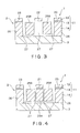
- Fig. 3 is a cross sectional view, taken along line II-II, of the sensor shown in Fig. 1
- Fig. 4 is a cross sectional view, taken along line III-III, of the sensor shown in Fig. 1 .
- the sensor 1 includes a sensor body 2 and a supporting substrate 3 joined to the sensor body 2.
- the sensor body 2 is formed of an SOI (Silicon On Insulator) substrate 11 having a three-layer structure including a silicon-oxide layer 13 interposed between a silicon layer 12 (or active-layer silicon) and another silicon layer 14 (or base silicon).
- Fig. 5 is a perspective view of the sensor 1 shown in Fig. 1
- Fig. 6 is another perspective view of the sensor 1 shown in Fig. 1 , in which the silicon-oxide layer 13 is separated from the silicon layer 14 (or base silicon), while the supporting substrate 3 is separated from the silicon layer 14 (or base silicon).
- the silicon layer 12 (or active-layer silicon), i.e., one component of the sensor body 2, includes a weight junction 21, four beams 22 respectively supporting the weight junction 21, a frame 23, and four windows 24 respectively surrounded by the beams 22 and frame 23.
- the four beams 22 are provided with piezo-resistance elements 28, respectively.
- piezo-resistance elements 28x each adapted for detecting external force applied in an X-axial direction
- four piezo-resistance elements 28y each adapted for detecting the external force applied in a Y-axial direction
- four piezo-resistance elements 28z each adapted for detecting the external force applied in a Z-axial direction
- the silicon layer 14 which is another component of the sensor body 2, includes a weight 25 and a frame 26 located around the weight 25 via an opening 27.
- the weight 25 has a thickness less than the thickness of the frame 26, and includes a base portion 25A and four projections 25B, each projecting from the base portion 25A toward a space between the crossing beams 22.
- the base portion 25A of the weight 25 is joined to the weight junction 21 of the silicon layer 12 (or active-layer silicon) via the silicon-oxide layer 13.
- the weight 25 when some external force is applied, in the X-axial, Y-axial or Z-axial direction, to the weight 25 supported by the four beams 22, the weight 25 will be displaced in the same direction. With such displacement, each beam 22 will be bent. Consequently, the external force applied to the weight 25 can be detected by the respective piezo-elements 28.
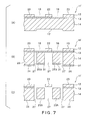
- Figs. 7(A)-7(C) are views showing one exemplary procedure of the method according to the present invention, in which the sensor body 2 of the sensor 1 is manufactured. It is noted that Figs. 7(A)-7(C) illustrate parts corresponding to the cross section shown in Fig. 3 . In Figs. 7(A)-7(C) , a necessary multi-faced process is performed on an SOI wafer 11' having the three-layer structure composed of the silicon layer 12 (or active-layer silicon), silicon-oxide layer 13 and silicon layer 14 (or base silicon).
- grooves 16 are formed in the silicon layer 12 (or active-layer silicon) in order to form the weight junction 21, beams 22 and frame 23, while a recess 17 is formed in the silicon layer 14 (or base silicon) in order to provide a desired thickness of the weight 25 (see Fig. 7(A) ).
- the formation of the grooves 16 and recess 17 can be performed, for example, by the so-called DRIE (Deep Reactive Ion Etching) method, i.e., a dry-etching method utilizing plasma, via a mask pattern.
- the grooves 16 and recess 17 may be formed by a sand-blast method, a wet-etching method, a femto-second-laser method or the like.
- the opening 27 is formed by processing the silicon layer 14 (or base silicon) on the side of the recess 17 of the SOI wafer 11', via a mask pattern 31, until the silicon-oxide layer 13 is exposed.
- the weight 25 or base portion 25A and projections 25B
- frame 26 can be formed, respectively (see Fig. 7(B) ).
- each portion of the silicon layer 13, exposed to the opening 27 and the grooves 16, is removed (see Fig. 7(C) ). In this way, the sensor body 2 can be obtained.
- the formation of the opening 27 can be performed, for example, by the DRIE method, via the mask pattern 31.
- the silicon-oxide layer 13 can be removed, for example, by an appropriate dry-etching process using a proper reactive gas.
- the method for forming the mask pattern 31 is not limited in particular. Any suitable method for forming such a mask pattern, such as by employing photolithography using a photosensitive resist or by forming a proper resin layer and/or metal layer on the wafer and then directly patterning the formed resin layer by utilizing laser plotting, or the like, can be used.
- the method of this invention is designed for correcting the mask pattern 31, such that formation or occurrence of a tapered portion and/or tilted portion in each opening 27 can be appropriately controlled when the opening 27 is formed by the DRIE method, via the mask pattern 31, on the side of the silicon layer 14 (base silicon). Now, this method will be described more specifically.
- Fig. 8 is a plan view of the sensor 1 when it is seen on the side of the silicon layer 14 (or base silicon) having the opening 27 (shown in Fig. 7(B) ) formed therein
- Fig. 9 is a cross section taken along line IV-IV shown in Fig. 8 .
- the mask pattern 31 is not shown in Fig. 8 .
- the opening 27 formed by the DRIE method usually includes the tapered portion expanded or spread toward the silicon-oxide layer 13 (for convenience, however, the opening 27 is not tapered in Figs. 2 through 7 ).
- a width b of a deeper portion of the opening 27 (i.e., the width of a region from which the silicon-oxide layer 13 is exposed) is usually greater than a width a of the opening in a surface at which the etching process is started (i.e., the width of a corresponding opening of the mask pattern 31).
- a tapered portion makes it difficult to form the weight as designed in advance.
- the degree or size of the tapered portion tends to be greater as one goes toward the central portion of the SOI wafer 11', due to distribution or change of the etching speed in the surface of the SOI wafer 11'. Further, this tendency varies with an apparatus used for the etching, conditions of the etching process, and the thickness of the SOI wafer 11'.
- the method of this invention is intended for controlling the tapered portion, by setting the width of the opening of the mask pattern 31 to be narrower (as depicted by a' in Fig. 9 ), such that the width of the deeper portion of the opening 27 (i.e., the width of the region from which the silicon-oxide layer 13 is exposed) can be changed into a designed value (i.e., the width a, as shown in Fig. 9 , of the opening of the mask pattern 31).
- the etching process is first performed, by using a predetermined apparatus under desired conditions, with the mask pattern set at the designed value thereof and hence not yet corrected for the tapered portion.
- Fig. 10 is a graph showing one example of the measured distribution of the size of expansion, wherein the origin is the center of the SOI. wafer 11' (having a thickness of 626 ⁇ m), the X-axis expresses a distance from the center of the SOI wafer 11', and the Y-axis designates the size of expansion relative to the distance in the X-axial direction. As shown in Fig.
- a desired amount t (see Fig. 9 ) of correction for narrowing the width of the opening of the mask pattern in a position at a distance r from the center of the SOI wafer 11' can be obtained by the following equation.
- the correction amount t is set on both sides of a center line 31a (see Figs. 11(B) and 11(C) ) of the opening of the mask pattern 31.
- Figs. 11(B) and 11(C) show a pattern of the opening (or opening pattern) of the mask pattern 31, respectively, wherein the opening pattern is designated by oblique lines.
- the mask pattern 31 includes an opening portion 36 having a corridor-like shape and four opening portions 32 projected inward from the corridor-like opening portion 36.
- the size of expansion (b-a) of the tapered portion can be obtained, on the assumption that the value a designates the designed value of the width of the opening in the surface at which the etching process is started, while the value b designates the width of the etched deeper portion of the opening actually measured by taking a photograph thereof by using a metallurgical microscope.
- Fig. 12 is a cross section taken along line V-V shown in Fig. 8 .
- an unwanted tilted portion is also formed when the opening 27 is formed by the DRIE method.
- the center of the deeper portion of the formed opening i.e., the region from which the silicon-oxide layer of the SOI wafer is exposed
- the center of the deeper portion of the formed opening is shifted toward the periphery of the SOI wafer 11' relative to the center of the opening in the surface at which the etching process is started (or opening of the mask pattern 31).
- the tilted portion is not shown in Figs. 2 through 7 .
- the center of gravity of the weight is substantially shifted from a designed position thereof.
- the weight junction 21 can be joined to the weight 25, while the center of gravity G of the weight 25 can be positioned such that each length of the two beams 22 respectively supporting the weight junction 21 can be equally set as designed in advance (i.e., corresponding to the length defined between two dotted lines L 1 , L 2 ).
- the tilted portion is formed as shown in Fig.
- the joined portion between the weight junction 21 and the weight 25 as well as the center of gravity G of the weight 25 are shifted from designed positions thereof (as designated by the two dotted lines L 1 , L 2 ), respectively.
- the length of the two beams 22 respectively supporting the weight junction 21 should be different from each other.
- the degree or size c (see Fig. 12 ) of such a tilted portion tends to be increased as one goes toward the periphery of the SOI wafer 11'. Further, this tendency varies with the apparatus used for the etching, conditions of the etching process, the thickness of the SOI wafer 11' and the like.
- Fig. 14 shows the opening pattern of the mask pattern 31, wherein the opening pattern is designated by oblique lines.
- the mask pattern 31 includes the corridor-like opening portion 36 and four opening portions 32 projected inward from the corridor-like opening portion 36.
- the four opening portions 32 are respectively provided for forming the opening 27 configured for separating the four projections 25B respectively constituting the weight 25, while defining the joined portion between the base portion 25A constituting the weight 25 and the weight junction 21.
- the length of each beam 22 is also determined by the opening portions 32.
- the aforementioned 100% correction is provided to regions 32a, 32b respectively depicted by thick lines in the mask pattern 31, while the 50% correction is provided to the other regions of the mask pattern 31.
- the etching process is first performed, by using a predetermined apparatus under desired conditions, with the mask pattern set at the designed value thereof and hence not yet corrected for the tilted portion. Then, distribution of the size (tilting amount) c of the tilted portion (see Fig. 12 ) formed in the SOI wafer 11' is measured. Fig.
- the correction amount C of the width of the opening of the mask pattern, in a position corresponding to a position vector r having coordinates (x, y) relative to the center of the SOI wafer 11' can be obtained as the following equations (2-1) and (2-2), in which the correction amount in the X-axial direction is expressed by C x , while the correction amount in the Y-axial direction is expressed by C y .
- C x kx
- C y ky
- the correction amount C of the width of the opening of the mask pattern, in the position corresponding to the vector r having coordinates (x, y) relative to the center of the SOI wafer 11' can be obtained as the following equations (3-1) and (3-2), in which the correction amount in the X-axial direction is expressed by C x , while the correction amount in the Y-axial direction is expressed by C y .
- C x k 1 ⁇ x 2 + y 2 1 / 2 ⁇ x + k 2 ⁇ x
- C y k 1 ⁇ x 2 + y 2 1 / 2 ⁇ y + k 2 ⁇ y
- the distribution of the size c of the tilted portion shown in Fig. 15 might be seen as a cubic curve on the Cartesian coordinate system, it can be rather approximated by the quadratic curve as described above on the polar coordinate system.
- Figs. 17(B) and 17(C) show the opening pattern of the mask pattern 31, respectively, wherein the opening pattern is designated by oblique lines.
- the mask pattern 31 includes the opening portion 36 having the corridor-like shape and the four opening portions 32 projected inward from the corridor-like opening portion 36.
- the opening pattern can be used as one designed in advance.
- the amount of correction for the tilted portion relative to the designed value (desired value) thereof is set, by using the equations (2-1) and (2-2) or equations (3-1) and (3-2).
- the 100% correction (C x , C y ) is performed for the regions 32a, 32b respectively depicted by thick lines in the mask pattern 31, while the 50% correction is provided to the other regions of the mask pattern 31.
- the openings 32, 36 of the mask pattern 31 will have shapes as shown in Fig. 17(C) , respectively. It is noted that the shapes depicted by dotted lines in Fig. 17(C) designate the opening pattern corresponding to the designed value (i.e., the opening pattern at the center P 0 ), respectively.
- the size c of the tilted portion can be determined by forming a hole shallower (e.g., having a 1 ⁇ m depth) and greater (in the diameter) than each opening to be formed, in advance, in an opposite surface of the wafer (i.e., a surface opposite to the surface from which the etching process is started). Then, the opening is formed by etching the wafer, with the center of this shallower hole being coincident with the center of the opening of the mask pattern. Thereafter, the amount of shift of the center of the opening formed by the etching process from the center of the shallower hole is obtained by taking an image of the deeper portion of the so-formed opening, by using the metallurgical microscope.
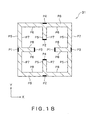
- each amount (h 1 to h 8 ) of correction of the regions P1 to P8 can be expressed as follows.
- each correction amount h 1 to h 8 of the regions P1 to P8 is a positive value, the correction will be performed in the positive direction in the X-axial direction or Y-axial direction, and that if each correction amount h 1 to h 8 is a negative value, the correction is performed in the negative direction in the X-axial direction or Y-axial direction.
- the present invention is not limited to the above embodiment.
- a metal mask or the like having a desired opening may be provided, in place of the mask pattern 31, in the vicinity of the silicon layer 14 (or base silicon).
- this invention is also applicable to the capacitance-type acceleration sensor and/or angular velocity sensor.
- the SOI wafer has been discussed, as an object to be etched, in the method of this invention for correcting the mask pattern, this method can be applied to any other suitable object, such as a silicon wafer, a metallic substrate or the like, to which the dry-etching process can be provided.
- the present invention can be applied to various fields, for which a high-precision dry-etching process is required, and also applied to various field, for which a significantly small-sized and highly reliable acceleration sensor and/or angular velocity sensor is required.
Landscapes
- Physics & Mathematics (AREA)
- General Physics & Mathematics (AREA)
- Engineering & Computer Science (AREA)
- Radar, Positioning & Navigation (AREA)
- Remote Sensing (AREA)
- Manufacturing & Machinery (AREA)
- Pressure Sensors (AREA)
- Gyroscopes (AREA)
- Preparing Plates And Mask In Photomechanical Process (AREA)
- Drying Of Semiconductors (AREA)
Abstract



Description
- The present invention relates to a method for correcting a mask pattern used for dry-etching a silicon wafer or the like, and also relates to a method for manufacturing an acceleration sensor and/or angular velocity sensor by using the method for correcting the mask pattern.
- In recent years, development of a small-sized sensor utilizing the so-called MEMS (Micro Electromechanical Systems) technology has been advanced, wherein application of a sensor for detecting acceleration and/or angular velocity to various devices or machines, such as portable phones and/or game machines, has been studied. Generally, the acceleration sensor and/or angular velocity sensor of this type is manufactured by using an SOI wafer having a three-layer structure composed of a silicon layer, a silicon-oxide layer and another silicon layer. More specifically, the sensor of this type includes a frame having an opening (or through hole) provided to extend through the SOI wafer, and a weight supported by the frame via a plurality of beams and provided to be displaced when applied with external force. Namely, when the external force (i.e., the acceleration or angular velocity) is applied to the weight, this sensor serves to measure such acceleration or angular velocity by detecting displacement of the weight (
Patent Documents 1 and 2).
For instance, the sensor for measuring the acceleration by detecting the displacement includes a piezo-resistance-type sensor, which has piezo-resistance elements respectively provided to the beams and is adapted for detecting change of resistance caused by bending of each beam, and a capacitance-type sensor adapted for detecting change of capacitance associated with the displacement of the weight.
While the sensor for measuring the angular velocity by detecting the displacement has substantially the same configuration as the capacitance-type one, the weight of this sensor is grounded and designed to be moved in a simple harmonic manner when an alternating current is applied to an associated counter electrode. Thus, this sensor is configured to detect the Coriolis force from the change of capacitance caused by the application of the external force to the sensor. - Patent Document 1:
JP2003-329702A - Patent Document 2:
JP2004-144598A - The conventional MEMS-type sensor as described above is provided to the SOI wafer in a multiple pattern. In this case, in a step of forming each weight, a dry-etching process, such as DRIE (Deep Reactive Ion Etching) or the like, is employed for etching the silicon layer by using a reactive gas excited by plasma.
However, in a usual dry-etching process provided to the silicon wafer, the plasma may tend to be non-uniform in the surface of the silicon wafer, resulting in some in-plane distribution of the plasma changing from the center of the silicon wafer toward the periphery thereof. Thus, an unwanted tapered and/or tilted portion is formed in each necessary hole or opening formed by the etching. This leads to deterioration of accuracy of the etching.
Similarly, such a tapered and/or tilted portion is also formed upon the formation of each weight by the dry-etching process provided to the SOI wafer. Namely, in each tapered portion of the etched silicon wafer, the width of a deeper portion of the hole or opening formed by the etching (i.e., a region from which the silicon-oxide layer of the SOI wafer is exposed) tends to be greater than the width of the opening in the surface of the wafer at which the etching process is started. Accordingly, such a tapered portion should make it difficult to form each weight as designed in advance. For instance, if an etching speed of an etching apparatus used for the etching process is increased as one goes toward a central portion of the SOI wafer, the degree or size of the tapered portion will be greater toward the central portion of the wafer. - Meanwhile, the formation of the tilted portions can be attributed to the fact that the direction in which the reactive gas penetrates into the silicon layer is not always vertical to the surface of the SOI wafer. Namely, the center of the deeper portion of each formed opening (i.e., the region from which the silicon-oxide layer of the SOI wafer is exposed) tends to be shifted toward the periphery of the wafer, relative to the center of the opening in the surface at which the etching process is started. Such a tilted portion should shift the center of gravity of each weight from a designed position (desired position) thereof, leading to deterioration of operational properties of the sensor. The degree or size of such a tilted portion will be increased as one goes toward the periphery of the SOI wafer.
It is true that the degree or size of such tapered and tilted portions depends on the apparatus used for the etching process, conditions of the process, thickness of the silicon wafer and/or SOI wafer, and the like. However, it is quite difficult to successfully prevent the formation of the tapered and tilted portions, by only controlling the apparatus and/or process conditions. - The present invention was made in light of the above circumstances, and therefore it is an object of this invention to provide a new method for correcting the mask pattern used for dry-etching an object, such as the silicon wafer or the like, with higher accuracy. Another object of this invention is to provide a new method for readily manufacturing the acceleration sensor and/or angular velocity sensor, each having a significantly small size and excellent reliability.
- The present invention is a method for correcting a mask pattern having an opening used for dry-etching, wherein the method is designed for correcting a width of the opening of the mask pattern, and wherein the method comprises: etching an object to be etched, by dry-etching, with a desired etching apparatus using a reference mask pattern which is not yet corrected, and then measuring distribution of the size of expansion of a tapered portion formed in a surface of the object to be etched; and approximating the measured distribution by using a quadratic curve (Y = AX2+B), so as to determine A and B, and then setting an amount t of correction for the tapered portion, expressed by the following equation (1) and related to the width of the opening of the mask pattern in a position at a distance r from a center of the object to be etched, thereby performing the correction for the tapered portion, such that the width of the opening can be set narrower than a designed value (desired value) thereof.

- The method for correcting the mask pattern according to this invention further comprises: measuring distribution of the size of a tilted portion formed in the surface of the object to be etched; and (A) approximating the measured distribution by using a straight line (Y = kX), so as to determine k (k>0), and then setting an amount Cx of correction in the X-axial direction and an amount Cy of correction in the Y-axial direction, respectively expressed by the following equations (2-1) and (2-2) and related to the width of the opening of the mask pattern in a position corresponding to a position vector r having coordinates (x, y) relative to the center of the object to be etched, thereby performing the correction for the tilted portion, based on the amounts Cx and Cy of correction:


(B) approximating the measured distribution by using a quadratic curve (Y = k1X2+k2X), so as to determine k1, k2 (k1>0, k2>0), and then setting the amount Cx of correction in the X-axial direction and the amount Cy of correction in the Y-axial direction, respectively expressed by the following equations (3-1) and (3-2) and related to the width of the opening of the mask pattern in the position corresponding to the position vector r having coordinates (x, y) relative to the center of the object to be etched, thereby performing the correction for the tilted portion, based on the amounts Cx and Cy of correction.

- Alternatively, the present invention is a method for manufacturing an acceleration sensor or an angular velocity sensor, comprising: dividing an SOI wafer having a three-layer structure composed of a silicon layer (or active-layer silicon), a silicon-oxide layer and another silicon layer (or base silicon), into multiple faces, and then providing a frame, a plurality of beams respectively projecting inward from the frame and a weight junction supported by the beams, to the silicon layer (or active-layer silicon), for each divided face of the SOI wafer; forming another frame and a weight to the silicon layer (or base silicon), the weight being positioned inside the frame, in a non-contact manner to the frame, and joined to and held by the weight junction via the silicon-oxide layer; then removing the silicon-oxide layer exposed to the outside; and joining a supporting substrate to the frame of the silicon layer (or base silicon), in a non-contact manner to the weight, wherein, in forming the frame and weight to the silicon layer (or base silicon), the frame and weight are formed, respectively, by forming an opening, by dry-etching the silicon layer (or base silicon), via a mask pattern having a corresponding opening, until the silicon-oxide layer is exposed, wherein the mask pattern has been corrected, in advance, to have a desired width of the opening thereof, and wherein the correction of the mask pattern comprises: etching an object to be etched, by dry-etching, with a desired etching apparatus using a reference mask pattern which is not yet corrected, and then measuring distribution of the size of expansion of a tapered portion formed in a surface of the object to be etched; and approximating the measured distribution by using a quadratic curve (Y = AX2+B), so as to determine A and B, and then setting an amount t of correction for the tapered portion, expressed by the following equation (1) and related to the width of the opening of the mask pattern in a position at a distance r from a center of the object to be etched, thereby performing the correction for the tapered portion, such that the width of the opening can be set narrower than a designed value thereof.

- The method for manufacturing the acceleration sensor and angular velocity sensor according to this invention further comprises: measuring distribution of the size of a tilted portion formed in the object to be etched; and (A) approximating the measured distribution by using a straight line (Y = kX), so as to determine k (k>0), and then setting an amount Cx of correction in the X-axial direction and an amount Cy of correction in the Y-axial direction, respectively expressed by the following equations (2-1) and (2-2) and related to the width of the opening of the mask pattern in a position corresponding to a position vector r having coordinates (x, y) relative to the center of the object to be etched, thereby performing the correction for the tilted portion, based on the amounts Cx and Cy of correction:


(B) approximating the measured distribution by using a quadratic curve (Y = k1X2+k2X), so as to determine k1, k2 (k1>0, k2>0), and then setting the amount Cx of correction in the X-axial direction and the amount Cy of correction in the Y-axial direction, respectively expressed by the following equations (3-1) and (3-2) and related to the width of the opening of the mask pattern in the position corresponding to the position vector r having the coordinates (x, y) relative to the center of the object to be etched, thereby performing the correction for the tilted portion, based on the amounts Cx and Cy of correction.

- In the method for manufacturing the acceleration sensor and angular velocity sensor according to this invention, the correction for the tilted portion, related to the width of the opening of the mask pattern, is performed, by setting an amount of correction for the tilted portion to be expressed by Cx and Cy, in regions having influence on the length of the corresponding beam, while setting the amount of correction for the tilted portion to be expressed by Cx/2 and Cy/2 in the other regions.
- As described above, the method according to the present invention is intended to control the formation of the tapered portion and tilted portion, not by controlling the apparatus and/or conditions employed or selected for the dry-etching process, but by correcting the opening of the mask pattern used for the dry-etching process, based on the distribution of the tapered portion and tilted portion, respectively detected in the surface of the wafer and peculiar to such apparatus and conditions. With this method, the dry-etching process can be provided to the silicon wafer with higher accuracy, thus achieving significantly accurate position control for the length of each beam as well as for the center of gravity of the weight. Additionally or alternatively, this invention is intended for providing the method for manufacturing the acceleration sensor and/or angular velocity sensor having a significantly small size and higher reliability.
-
-
Fig. 1 is a plan view of a piezo-resistance-type acceleration sensor, which is one example of sensors manufactured by a method according to the present invention. -
Fig. 2 is a cross sectional view, taken along line I-I, of the sensor shown inFig. 1 . -
Fig. 3 is a cross sectional view, taken along line II-II, of the sensor shown inFig. 1 . -
Fig. 4 is a cross section, taken along line III-III, of the sensor shown inFig. 1 . -
Fig. 5 is a perspective view of the sensor shown inFig. 1 . -
Fig. 6 is another perspective view of the sensor shown inFig. 1 , in which a silicon-oxide layer is separated from a silicon layer (or base silicon), while a supporting substrate is separated from the silicon layer (or base silicon). -
Figs. 7(A) through 7(C) are views, respectively showing one exemplary procedure of the method for manufacturing the sensor related to the present invention. -
Fig. 8 is a plan view of the sensor when it is seen on the side of the silicon layer (or base silicon) having an opening (shown inFig. 7(B) ) formed therein. -
Fig. 9 is a cross sectional view taken along line IV-IV shown inFig. 8 . -
Fig. 10 is a graph showing one example of distribution of the size of expansion of a tapered portion. -
Figs. 11(A) to 11(C) are views, each illustrating correction for the tapered portion, related to an opening of a mask pattern, whereinFig. 11(A) shows an SOI wafer,Fig. 11(B) shows the mask pattern located at a point P0 at a center of the SOI wafer, andFig. 11(C) shows the mask pattern located at a point P at a distance r from the center. -
Fig. 12 is a cross sectional view taken along line V-V shown inFig. 8 . -
Figs. 13(A) to 13(D) are views showing state in which tilted portions are formed, as well as illustrating correction for the tilted portions. -
Fig. 14 is a view showing a pattern of the opening of the mask pattern. -
Fig. 15 is a graph showing distribution of the size of the tilted portion, as well as illustrating one exemplary approximation of the distribution by using a straight line. -
Fig. 16 is a graph showing another example of the distribution of the size of the tilted portion, as well as illustrating the approximation thereof by using a quadratic-curve. -
Figs. 17(A) to 17(C) are views, each illustrating the correction for the tapered portion, related to the opening of the mask pattern, whereinFig. 17(A) shows the SOI wafer,Fig. 17(B) shows the mask pattern located at the point P0 at the center of the SOI wafer, andFig. 17(C) shows the mask pattern located at the point P at the distance r from the center. -
Fig. 18 is a view illustrating each amount of correction for the tapered portion and tilted portion, related to the mask pattern. - Hereinafter, one exemplary embodiment of the present invention will be described, with reference to the drawings.
Fig. 1 is a plan view of a piezo-resistance-type acceleration sensor, which is one example of sensors manufactured by a method according to the present invention,Fig. 2 is a cross section, taken along line I-I, of the sensor shown inFig. 1 ,Fig. 3 is a cross sectional view, taken along line II-II, of the sensor shown inFig. 1 , andFig. 4 is a cross sectional view, taken along line III-III, of the sensor shown inFig. 1 . In these drawings, thesensor 1 includes asensor body 2 and a supportingsubstrate 3 joined to thesensor body 2. Thesensor body 2 is formed of an SOI (Silicon On Insulator)substrate 11 having a three-layer structure including a silicon-oxide layer 13 interposed between a silicon layer 12 (or active-layer silicon) and another silicon layer 14 (or base silicon).Fig. 5 is a perspective view of thesensor 1 shown inFig. 1 , andFig. 6 is another perspective view of thesensor 1 shown inFig. 1 , in which the silicon-oxide layer 13 is separated from the silicon layer 14 (or base silicon), while the supportingsubstrate 3 is separated from the silicon layer 14 (or base silicon). - As shown in
Figs. 1 through 6 , the silicon layer 12 (or active-layer silicon), i.e., one component of thesensor body 2, includes aweight junction 21, fourbeams 22 respectively supporting theweight junction 21, aframe 23, and fourwindows 24 respectively surrounded by thebeams 22 andframe 23. The fourbeams 22 are provided with piezo-resistance elements 28, respectively. More specifically, four piezo-resistance elements 28x, each adapted for detecting external force applied in an X-axial direction, four piezo-resistance elements 28y, each adapted for detecting the external force applied in a Y-axial direction, and four piezo-resistance elements 28z, each adapted for detecting the external force applied in a Z-axial direction, are provided to the fourbeams 22, respectively. - The silicon layer 14 (or base silicon), which is another component of the
sensor body 2, includes aweight 25 and aframe 26 located around theweight 25 via anopening 27. Theweight 25 has a thickness less than the thickness of theframe 26, and includes abase portion 25A and fourprojections 25B, each projecting from thebase portion 25A toward a space between the crossing beams 22. Thebase portion 25A of theweight 25 is joined to theweight junction 21 of the silicon layer 12 (or active-layer silicon) via the silicon-oxide layer 13.
In thesensor 1 as described above, when some external force is applied, in the X-axial, Y-axial or Z-axial direction, to theweight 25 supported by the fourbeams 22, theweight 25 will be displaced in the same direction. With such displacement, eachbeam 22 will be bent. Consequently, the external force applied to theweight 25 can be detected by the respective piezo-elements 28. -
Figs. 7(A)-7(C) are views showing one exemplary procedure of the method according to the present invention, in which thesensor body 2 of thesensor 1 is manufactured. It is noted thatFigs. 7(A)-7(C) illustrate parts corresponding to the cross section shown inFig. 3 .
InFigs. 7(A)-7(C) , a necessary multi-faced process is performed on an SOI wafer 11' having the three-layer structure composed of the silicon layer 12 (or active-layer silicon), silicon-oxide layer 13 and silicon layer 14 (or base silicon). First, for each face of the SOI wafer 11',grooves 16 are formed in the silicon layer 12 (or active-layer silicon) in order to form theweight junction 21, beams 22 andframe 23, while arecess 17 is formed in the silicon layer 14 (or base silicon) in order to provide a desired thickness of the weight 25 (seeFig. 7(A) ). The formation of thegrooves 16 andrecess 17 can be performed, for example, by the so-called DRIE (Deep Reactive Ion Etching) method, i.e., a dry-etching method utilizing plasma, via a mask pattern. Alternatively, thegrooves 16 andrecess 17 may be formed by a sand-blast method, a wet-etching method, a femto-second-laser method or the like. - Next, for each face of the SOI wafer 11', the
opening 27 is formed by processing the silicon layer 14 (or base silicon) on the side of therecess 17 of the SOI wafer 11', via amask pattern 31, until the silicon-oxide layer 13 is exposed. As a result, the weight 25 (orbase portion 25A andprojections 25B) andframe 26 can be formed, respectively (seeFig. 7(B) ). Thereafter, each portion of thesilicon layer 13, exposed to theopening 27 and thegrooves 16, is removed (seeFig. 7(C) ). In this way, thesensor body 2 can be obtained. The formation of theopening 27 can be performed, for example, by the DRIE method, via themask pattern 31. Meanwhile, the silicon-oxide layer 13 can be removed, for example, by an appropriate dry-etching process using a proper reactive gas. It is noted that the method for forming themask pattern 31 is not limited in particular. Any suitable method for forming such a mask pattern, such as by employing photolithography using a photosensitive resist or by forming a proper resin layer and/or metal layer on the wafer and then directly patterning the formed resin layer by utilizing laser plotting, or the like, can be used. - In this case, the method of this invention is designed for correcting the
mask pattern 31, such that formation or occurrence of a tapered portion and/or tilted portion in eachopening 27 can be appropriately controlled when theopening 27 is formed by the DRIE method, via themask pattern 31, on the side of the silicon layer 14 (base silicon). Now, this method will be described more specifically. - First, as the method for controlling the formation of the tapered portion in each
opening 27, one method for manufacturing thesensor 1 while correcting the mask pattern is described by way of example.Fig. 8 is a plan view of thesensor 1 when it is seen on the side of the silicon layer 14 (or base silicon) having the opening 27 (shown inFig. 7(B) ) formed therein, andFig. 9 is a cross section taken along line IV-IV shown inFig. 8 . For clarity, themask pattern 31 is not shown inFig. 8 . As shown inFig. 9 , theopening 27 formed by the DRIE method usually includes the tapered portion expanded or spread toward the silicon-oxide layer 13 (for convenience, however, theopening 27 is not tapered inFigs. 2 through 7 ). Namely, a width b of a deeper portion of the opening 27 (i.e., the width of a region from which the silicon-oxide layer 13 is exposed) is usually greater than a width a of the opening in a surface at which the etching process is started (i.e., the width of a corresponding opening of the mask pattern 31). Thus, such a tapered portion makes it difficult to form the weight as designed in advance. Besides, the degree or size of the tapered portion tends to be greater as one goes toward the central portion of the SOI wafer 11', due to distribution or change of the etching speed in the surface of the SOI wafer 11'. Further, this tendency varies with an apparatus used for the etching, conditions of the etching process, and the thickness of the SOI wafer 11'. - Thus, while allowing the formation of such a tapered portion, the method of this invention is intended for controlling the tapered portion, by setting the width of the opening of the
mask pattern 31 to be narrower (as depicted by a' inFig. 9 ), such that the width of the deeper portion of the opening 27 (i.e., the width of the region from which the silicon-oxide layer 13 is exposed) can be changed into a designed value (i.e., the width a, as shown inFig. 9 , of the opening of the mask pattern 31).
In this case, the etching process is first performed, by using a predetermined apparatus under desired conditions, with the mask pattern set at the designed value thereof and hence not yet corrected for the tapered portion. Then, distribution of the size of expansion of the tapered portion formed in the SOI wafer 11' (i.e., a difference (b-a) between the width b and the width a of the opening shown inFig. 9 ) is measured.Fig. 10 is a graph showing one example of the measured distribution of the size of expansion, wherein the origin is the center of the SOI. wafer 11' (having a thickness of 626µm), the X-axis expresses a distance from the center of the SOI wafer 11', and the Y-axis designates the size of expansion relative to the distance in the X-axial direction. As shown inFig. 10 , the size of expansion (i.e., b-a) of the tapered portion can be approximated by using a quadratic curve (Y=AX2+B) having a peak at the center of the SOI wafer 11'. For instance, the quadratic curve shown inFig. 10 can be expressed by Y=-0.00532·X2+106. Thus, a desired amount t (seeFig. 9 ) of correction for narrowing the width of the opening of the mask pattern in a position at a distance r from the center of the SOI wafer 11' can be obtained by the following equation.
center line 31a (seeFigs. 11(B) and 11(C) ) of the opening of themask pattern 31. - Accordingly, with respect to the center P0 of the SOI wafer 11' and a point P corresponding to the position at the distance r from the center P0 of the SOI wafer 11' as shown in
Fig. 11(A) , the correction for the tapered portion or narrowing the width of opening of themask pattern 31 is carried out, respectively, as shown inFigs. 11(B) and 11(C) . Namely,Figs. 11(B) and 11(C) show a pattern of the opening (or opening pattern) of themask pattern 31, respectively, wherein the opening pattern is designated by oblique lines. In these drawings, themask pattern 31 includes an openingportion 36 having a corridor-like shape and four openingportions 32 projected inward from the corridor-like opening portion 36. In this case, as shown inFig. 11(B) , the correction amount (to), at the center P0 of the SOI wafer 11', for the tapered portion, relative to the designed value, is expressed by t0 = B/2. Because the expansion of the tapered portion is the maximum at the point Po, the width of the openingportions mask pattern 31 at this point P0 should be set narrowest. Meanwhile, as shown inFig. 11(C) , the correction amount (t), at the point P, for the tapered portion, relative to the designed value, is expressed by t = (Ar2+B)/2.
It is noted that the size of expansion (b-a) of the tapered portion can be obtained, on the assumption that the value a designates the designed value of the width of the opening in the surface at which the etching process is started, while the value b designates the width of the etched deeper portion of the opening actually measured by taking a photograph thereof by using a metallurgical microscope. - Next, as the method for controlling the tilted portion in each
opening 27, one method for manufacturing thesensor 1 while correcting the mask pattern will be described by way of example.Fig. 12 is a cross section taken along line V-V shown inFig. 8 . Usually, as shown inFig. 12 , an unwanted tilted portion is also formed when theopening 27 is formed by the DRIE method. In such a tilted portion, the center of the deeper portion of the formed opening (i.e., the region from which the silicon-oxide layer of the SOI wafer is exposed) is shifted toward the periphery of the SOI wafer 11' relative to the center of the opening in the surface at which the etching process is started (or opening of the mask pattern 31). For convenience, however, the tilted portion is not shown inFigs. 2 through 7 . With formation of such a tilted portion, the center of gravity of the weight is substantially shifted from a designed position thereof. For instance, as shown inFig. 13(A) , if the tilted portion is not formed, theweight junction 21 can be joined to theweight 25, while the center of gravity G of theweight 25 can be positioned such that each length of the twobeams 22 respectively supporting theweight junction 21 can be equally set as designed in advance (i.e., corresponding to the length defined between two dotted lines L1, L2). However, if the tilted portion is formed as shown inFig. 13(B) , the joined portion between theweight junction 21 and theweight 25 as well as the center of gravity G of theweight 25 are shifted from designed positions thereof (as designated by the two dotted lines L1, L2), respectively. Thus, the length of the twobeams 22 respectively supporting theweight junction 21 should be different from each other. The degree or size c (seeFig. 12 ) of such a tilted portion tends to be increased as one goes toward the periphery of the SOI wafer 11'. Further, this tendency varies with the apparatus used for the etching, conditions of the etching process, the thickness of the SOI wafer 11' and the like. - Thus, while allowing the formation of such a tilted portion, the method of this invention is intended for controlling the tilted portion by correcting the mask pattern, in a combination of 50% correction (i.e., the correction amount = C/2) as shown in
Fig. 13(C) , in which the center of gravity G of theweight 25 is set in the designed position thereof (as designated by the dotted line L2) while the joined portion between theweight junction 21 and theweight 25 is shifted from the designed position thereof (as designated by the dotted line L1) and 100% correction (i.e., the correction amount = C) as shown inFig. 13(D) , in which the joined portion between theweight junction 21 and theweight 25 is set in the designed position thereof (as designated by the dotted line L1) while the center of gravity G of the weight is shifted from the designed position thereof (as shown in the dotted line L2).Fig. 14 shows the opening pattern of themask pattern 31, wherein the opening pattern is designated by oblique lines. As described above, themask pattern 31 includes the corridor-like opening portion 36 and four openingportions 32 projected inward from the corridor-like opening portion 36. The four openingportions 32 are respectively provided for forming theopening 27 configured for separating the fourprojections 25B respectively constituting theweight 25, while defining the joined portion between thebase portion 25A constituting theweight 25 and theweight junction 21. Therefore, the length of eachbeam 22 is also determined by the openingportions 32. Thus, in order to equally set the length of the fourbeams 22 supporting theweight junction 21, the aforementioned 100% correction is provided toregions mask pattern 31, while the 50% correction is provided to the other regions of themask pattern 31. - In this correction for the tilted portion, the etching process is first performed, by using a predetermined apparatus under desired conditions, with the mask pattern set at the designed value thereof and hence not yet corrected for the tilted portion. Then, distribution of the size (tilting amount) c of the tilted portion (see
Fig. 12 ) formed in the SOI wafer 11' is measured.
Fig. 15 is a graph showing one example of the distribution of the size (tilting amount) c of the tilted portion, wherein the origin designates the center of the SOI wafer 11' (having a thickness of 626µm), the X-axis expresses the distance from the center of the SOI wafer 11', while the Y-axis designates the distribution of the size of the tilted portion. If the distribution of the size (tilting amount) c of the tilted portion is approximated by using a straight line (Y = kX) passing through a central portion of the SOI wafer 11', as shown inFig. 15 , this line can be expressed by, for example, Y = 0.17X. Accordingly, the correction amount C of the width of the opening of the mask pattern, in a position corresponding to a position vector r having coordinates (x, y) relative to the center of the SOI wafer 11', can be obtained as the following equations (2-1) and (2-2), in which the correction amount in the X-axial direction is expressed by Cx, while the correction amount in the Y-axial direction is expressed by Cy.

- Alternatively, if the distribution of the size c of the tilted portion is approximated by using a quadratic curve (Y = k1X2+k2X) passing through the central portion of the SOI wafer 11', as shown in
Fig. 16 , this curved line can be expressed by, for example, Y = 0.0012X2+0.080X. In this case, the correction amount C of the width of the opening of the mask pattern, in the position corresponding to the vector r having coordinates (x, y) relative to the center of the SOI wafer 11', can be obtained as the following equations (3-1) and (3-2), in which the correction amount in the X-axial direction is expressed by Cx, while the correction amount in the Y-axial direction is expressed by Cy.

Fig. 15 might be seen as a cubic curve on the Cartesian coordinate system, it can be rather approximated by the quadratic curve as described above on the polar coordinate system. - Accordingly, the correction for the tilted portion, at the center P0 of the SOI wafer 11' and the point P(x, y) at the distance r from the center of the SOI wafer 11', respectively shown in
Fig. 17(A) , can be shown inFigs. 17(B) and 17(C) , respectively. Namely,Figs. 17(B) and 17(C) show the opening pattern of themask pattern 31, respectively, wherein the opening pattern is designated by oblique lines. Again, themask pattern 31 includes the openingportion 36 having the corridor-like shape and the four openingportions 32 projected inward from the corridor-like opening portion 36. As shown inFig. 17(B) , since the tilted portion is not formed at center P0 of the SOI wafer 11', the correction for the tilted portion in this position is not necessary (i.e., Cx = 0, Cy = 0). Thus, the opening pattern can be used as one designed in advance. Meanwhile, at the point P(x, y), the amount of correction for the tilted portion relative to the designed value (desired value) thereof is set, by using the equations (2-1) and (2-2) or equations (3-1) and (3-2). In addition, as shown inFig. 14 , the 100% correction (Cx, Cy) is performed for theregions mask pattern 31, while the 50% correction is provided to the other regions of themask pattern 31. Thus, theopenings mask pattern 31 will have shapes as shown inFig. 17(C) , respectively. It is noted that the shapes depicted by dotted lines inFig. 17(C) designate the opening pattern corresponding to the designed value (i.e., the opening pattern at the center P0), respectively. - For instance, the size c of the tilted portion can be determined by forming a hole shallower (e.g., having a 1µm depth) and greater (in the diameter) than each opening to be formed, in advance, in an opposite surface of the wafer (i.e., a surface opposite to the surface from which the etching process is started). Then, the opening is formed by etching the wafer, with the center of this shallower hole being coincident with the center of the opening of the mask pattern. Thereafter, the amount of shift of the center of the opening formed by the etching process from the center of the shallower hole is obtained by taking an image of the deeper portion of the so-formed opening, by using the metallurgical microscope. It is noted that whether the distribution of the size of the tilted portion is approximated by the straight line (Y = kX) or by the quadratic curve (Y = k1X2+k2X) can be optionally determined from each state of the distribution of the size of the tilted portion. However, it should be appreciated that if the distribution of the size of the tilted portion tends to show a profile like a quadratic function, the approximation with a proper quadratic curve can be selected for setting the correction amount more accurately.
- Next, the mask pattern that is corrected for the tapered portion and tilted portion will be described.
As described above, at the center P0(0, 0) of the SOI wafer 11' shown inFig. 17(A) , only the correction for the tapered portion is performed, while the correction for the tilted portion is not required. Meanwhile, at the point P(x, y) located at the distance r from the center of the SOI wafer 11', the correction for both of the tapered portion and tilted portion should be performed. Now, the correction for both of the tapered portion and tilted portion, related to each region or part of themask pattern 31 at the point P(x, y), will be described in more detail with reference toFig. 18 . In themask pattern 31 located at the point P(x, y), eight regions, respectively designated by P1 to P8, are first set as shown inFig. 18 , depending on difference in positions in the X-axial direction and Y-axial direction, i.e., depending on difference in regions respectively corrected by utilizing the 50% correction and 100% correction for the tilted portion. Then, the correction for the tapered portion and/or tilted portion is performed for each set region. Specifically, the regions P1 to P4 are respectively provided with the 100% correction for the tilted portion, while P5 to P8 are subjected to the 50% correction for the tilted portion. Namely, each amount (h1 to h8) of correction of the regions P1 to P8 can be expressed as follows. -


- It is noted that if each correction amount h1 to h8 of the regions P1 to P8 is a positive value, the correction will be performed in the positive direction in the X-axial direction or Y-axial direction, and that if each correction amount h1 to h8 is a negative value, the correction is performed in the negative direction in the X-axial direction or Y-axial direction.
It should be appreciated that the present invention is not limited to the above embodiment. For instance, while themask pattern 31 has been formed on the silicon layer 14 (or base silicon) of the SOI wafer 11' in the above embodiment, a metal mask or the like having a desired opening may be provided, in place of themask pattern 31, in the vicinity of the silicon layer 14 (or base silicon).
In addition, while the piezo-resistance-type acceleration sensor has been discussed by way of example in the above embodiment, this invention is also applicable to the capacitance-type acceleration sensor and/or angular velocity sensor.
Furthermore, while the SOI wafer has been discussed, as an object to be etched, in the method of this invention for correcting the mask pattern, this method can be applied to any other suitable object, such as a silicon wafer, a metallic substrate or the like, to which the dry-etching process can be provided. - The present invention can be applied to various fields, for which a high-precision dry-etching process is required, and also applied to various field, for which a significantly small-sized and highly reliable acceleration sensor and/or angular velocity sensor is required.
Claims (5)
- A method for correcting a mask pattern having an opening used for dry-etching, wherein the method is designed for correcting a width of the opening of the mask pattern, and
wherein the method comprises:etching an object to be etched, by dry-etching, with a desired etching apparatus using a reference mask pattern which is not yet corrected, and then measuring distribution of the size of expansion of a tapered portion formed in a surface of the object to be etched; andapproximating the measured distribution by using a quadratic curve (Y = AX2+B), so as to determine A and B, and then setting an amount t of correction for the tapered portion, expressed by the following equation (1) and related to the width of the opening of the mask pattern in a position at a distance r from a center of the object to be etched, thereby performing the correction for the tapered portion, such that the width of the opening can be set narrower than a designed value thereof.
- The method for correcting the mask pattern, according to claim 1, further comprising:measuring distribution of the size of a tilted portion formed in the surface of the object to be etched; and(A) approximating the measured distribution by using a straight line (Y = kX), so as to determine k (k>0), and then setting an amount Cx of correction in the X-axial direction and an amount Cy of correction in the Y-axial direction, respectively expressed by the following equations (2-1) and (2-2) and related to the width of the opening of the mask pattern in a position corresponding to a position vector r having coordinates (x, y) relative to the center of the object to be etched, thereby performing the correction for the tilted portion, based on the amounts Cx and Cy of correction:

 (B) approximating the measured distribution by using a quadratic curve (Y = k1X2+k2X), so as to determine k1, k2 (k1>0, k2>0), and then setting the amount Cx of correction in the X-axial direction and the amount Cy of correction in the Y-axial direction, respectively expressed by the following equations (3-1) and (3-2) and related to the width of the opening of the mask pattern in the position corresponding to the position vector r having coordinates (x, y) relative to the center of the object to be etched, thereby performing the correction for the tilted portion, based on the amounts Cx and Cy of correction.

- A method for manufacturing an acceleration sensor or an angular velocity sensor, comprising:dividing an SOI wafer having a three-layer structure composed of a silicon layer (or active-layer silicon), a silicon-oxide layer and another silicon layer (or base silicon), into multiple faces, and then providing a frame, a plurality of beams respectively projecting inward from the frame and a weight junction supported by the beams, to the silicon layer (or active-layer silicon), for each divided face of the SOI wafer;forming another frame and a weight to the silicon layer (or base silicon), the weight being positioned inside the frame, in a non-contact manner to the frame, and joined to and held by the weight junction via the silicon-oxide layer;removing the silicon-oxide layer exposed to the outside; andjoining a supporting substrate to the frame of the silicon layer (or base silicon), in a non-contact manner to the weight,wherein, in forming the frame and weight to the silicon layer (or base silicon), the frame and weight are formed, respectively, by forming an opening, by dry-etching the silicon layer (or base silicon), via a mask pattern having a corresponding opening, until the silicon-oxide layer is exposed,
wherein the mask pattern has been corrected, in advance, to have a desired width of the opening thereof, and
wherein the correction of the mask pattern comprises:
etching an object to be etched, by dry-etching, with a desired etching apparatus using a reference mask pattern which is not yet corrected, and then measuring distribution of the size of expansion of a tapered portion formed in a surface of the object to be etched; and
approximating the measured distribution by using a quadratic curve (Y = AX2+B), so as to determine A and B, and then setting an amount t of correction for the tapered portion, expressed by the following equation (1) and related to the width of the opening of the mask pattern in a position at a distance r from a center of the object to be etched, thereby performing the correction for the tapered portion, such that the width of the opening can be set narrower than a designed value thereof.
- The method for manufacturing the acceleration sensor and angular velocity sensor, according to claim 3, further comprising:measuring distribution of the size of a tilted portion formed in the object to be etched; and(A) approximating the measured distribution by using a straight line (Y = kX), so as to determine k (k>0), and then setting an amount Cx of correction in the X-axial direction and an amount Cy of correction in the Y-axial direction, respectively expressed by the following equations (2-1) and (2-2) and related to the width of the opening of the mask pattern in a position corresponding to a position vector r having coordinates (x, y) relative to the center of the object to be etched, thereby performing the correction for the tilted portion, based on the amounts Cx and Cy of correction:

 (B) approximating the measured distribution by using a quadratic curve (Y = k1X2+k2X), so as to determine k1, k2 (k1>0, k2>0), and then setting the amount Cx of correction in the X-axial direction and the amount Cy of correction in the Y-axial direction, respectively expressed by the following equations (3-1) and (3-2) and related to the width of the opening of the mask pattern in a position corresponding to the position vector r having the coordinates (x, y) relative to the center of the object to be etched, thereby performing the correction for the tilted portion, based on the amounts Cx and Cy of correction.

- The method for manufacturing the acceleration sensor and angular velocity sensor, according to claim 4, wherein the correction for the tilted portion, related to the width of the opening of the mask pattern, is performed, by setting the amount of correction for the tilted portion to be expressed by Cx and Cy, in regions having influence on the length of the corresponding beam, while setting the amount of correction for the tilted portion to be expressed by Cx/2 and Cy/2 in the other regions.
Applications Claiming Priority (2)
| Application Number | Priority Date | Filing Date | Title |
|---|---|---|---|
| JP2007289623A JP5186885B2 (en) | 2007-11-07 | 2007-11-07 | Mask pattern correction method and acceleration sensor and angular velocity sensor manufacturing method using the same |
| PCT/JP2008/069764 WO2009060781A1 (en) | 2007-11-07 | 2008-10-30 | Method for correcting mask pattern and method for manufacturing acceleration sensor and angular velocity sensor by using same |
Publications (3)
| Publication Number | Publication Date |
|---|---|
| EP2110847A1 true EP2110847A1 (en) | 2009-10-21 |
| EP2110847A4 EP2110847A4 (en) | 2012-05-09 |
| EP2110847B1 EP2110847B1 (en) | 2014-03-19 |
Family
ID=40625674
Family Applications (1)
| Application Number | Title | Priority Date | Filing Date |
|---|---|---|---|
| EP08847989.4A Not-in-force EP2110847B1 (en) | 2007-11-07 | 2008-10-30 | Method for manufacturing acceleration sensor and angular velocity sensor by using a method for correcting mask pattern |
Country Status (4)
| Country | Link |
|---|---|
| US (1) | US8241923B2 (en) |
| EP (1) | EP2110847B1 (en) |
| JP (1) | JP5186885B2 (en) |
| WO (1) | WO2009060781A1 (en) |
Families Citing this family (7)
| Publication number | Priority date | Publication date | Assignee | Title |
|---|---|---|---|---|
| JP5108617B2 (en) * | 2008-05-13 | 2012-12-26 | 大日本印刷株式会社 | Acceleration sensor |
| KR101299731B1 (en) * | 2012-05-29 | 2013-08-22 | 삼성전기주식회사 | Angular velocity sensor |
| KR101388814B1 (en) * | 2012-09-11 | 2014-04-23 | 삼성전기주식회사 | Angular Velocity Sensor |
| KR101366990B1 (en) * | 2012-12-28 | 2014-02-24 | 삼성전기주식회사 | Angular velocity sensor |
| KR101540154B1 (en) * | 2013-10-04 | 2015-07-28 | 삼성전기주식회사 | Angular Velocity Sensor and Manufacturing Method of the same |
| DE112015000515T5 (en) * | 2014-01-27 | 2016-11-10 | Panasonic Intellectual Property Management Co., Ltd. | accelerometer |
| FR3051973B1 (en) | 2016-05-24 | 2018-10-19 | X-Fab France | PROCESS FOR FORMING TRANSISTORS PDSOI AND FDSOI ON THE SAME SUBSTRATE |
Family Cites Families (8)
| Publication number | Priority date | Publication date | Assignee | Title |
|---|---|---|---|---|
| JPH0653170A (en) * | 1992-03-18 | 1994-02-25 | Nec Corp | Ecr plasma etcher |
| JPH07152147A (en) * | 1993-11-30 | 1995-06-16 | Sony Corp | Production and apparatus for producing mask for exposing |
| US6409147B1 (en) * | 2000-06-13 | 2002-06-25 | Thomas M. Kenny | Thermally operated valve for automatically modulating the flow of fluids |
| JP4216525B2 (en) | 2002-05-13 | 2009-01-28 | 株式会社ワコー | Acceleration sensor and manufacturing method thereof |
| AU2003290510A1 (en) * | 2002-06-26 | 2004-04-19 | Cornell Research Foundation, Inc. | Small scale wires with microelectromechanical devices |
| JP4248222B2 (en) | 2002-10-24 | 2009-04-02 | 株式会社ワコー | Angular velocity sensor |
| JP4179070B2 (en) * | 2003-06-25 | 2008-11-12 | 松下電工株式会社 | Semiconductor acceleration sensor and manufacturing method thereof |
| EP1491901A1 (en) | 2003-06-25 | 2004-12-29 | Matsushita Electric Works, Ltd. | Semiconductor acceleration sensor and method of manufacturing the same |
-
2007
- 2007-11-07 JP JP2007289623A patent/JP5186885B2/en not_active Expired - Fee Related
-
2008
- 2008-10-30 US US12/522,786 patent/US8241923B2/en not_active Expired - Fee Related
- 2008-10-30 EP EP08847989.4A patent/EP2110847B1/en not_active Not-in-force
- 2008-10-30 WO PCT/JP2008/069764 patent/WO2009060781A1/en not_active Ceased
Also Published As
| Publication number | Publication date |
|---|---|
| JP2009117642A (en) | 2009-05-28 |
| JP5186885B2 (en) | 2013-04-24 |
| EP2110847B1 (en) | 2014-03-19 |
| US20090305439A1 (en) | 2009-12-10 |
| WO2009060781A1 (en) | 2009-05-14 |
| EP2110847A4 (en) | 2012-05-09 |
| US8241923B2 (en) | 2012-08-14 |
Similar Documents
| Publication | Publication Date | Title |
|---|---|---|
| US8241923B2 (en) | Method for correcting mask pattern and method for manufacturing acceleration sensor and angular velocity sensor by using the method for correcting the mask pattern | |
| US10203351B2 (en) | MEMS accelerometer with Z axis anchor tracking | |
| KR0139506B1 (en) | Self-diagnostic accelerometer with symmetric proof-mass and its preparation method | |
| US8635909B2 (en) | Vibrating micromechanical sensor of angular velocity | |
| US9316665B2 (en) | Estimation of sidewall skew angles of a structure | |
| JP4693003B2 (en) | Processing method of micro-processing multi-sensor on substrate | |
| US7104128B2 (en) | Multiaxial micromachined differential accelerometer | |
| JP6052302B2 (en) | Angular acceleration sensor and acceleration sensor | |
| KR102452565B1 (en) | Design method of multi-axis MEMS gyro sensor with low cross-axis sensitivity | |
| JP4815857B2 (en) | Manufacturing method of mechanical quantity detection sensor | |
| JP4436096B2 (en) | Capacitive sensor and manufacturing method thereof | |
| CN102947216B (en) | Microelectromechanicdevices devices and application thereof | |
| US9964561B2 (en) | Acceleration sensor | |
| US20140283606A1 (en) | Acceleration sensor | |
| US6938487B2 (en) | Inertia sensor | |
| JP2006317242A (en) | Mechanical quantity detection sensor and manufacturing method thereof | |
| US20240003935A1 (en) | Physical Quantity Sensor And Inertial Measurement Unit | |
| JP2004330310A (en) | Fine shape fabrication method | |
| US20040226372A1 (en) | Hinge position location that causes pendulous axis to be substantially parallel with drive component direction | |
| JP4849369B2 (en) | Device manufacturing method and tilt sensor using the same | |
| KR20070072319A (en) | Method and device for measuring angular velocity using two acceleration sensors | |
| JP2001059850A (en) | Exercise state determination device, exercise state determination system, exercise state determination method, and method of manufacturing exercise state determination device | |
| JPH06222075A (en) | Acceleration sensor and air bag system and car body control system employing it |
Legal Events
| Date | Code | Title | Description |
|---|---|---|---|
| PUAI | Public reference made under article 153(3) epc to a published international application that has entered the european phase |
Free format text: ORIGINAL CODE: 0009012 |
|
| 17P | Request for examination filed |
Effective date: 20090723 |
|
| AK | Designated contracting states |
Kind code of ref document: A1 Designated state(s): AT BE BG CH CY CZ DE DK EE ES FI FR GB GR HR HU IE IS IT LI LT LU LV MC MT NL NO PL PT RO SE SI SK TR |
|
| DAX | Request for extension of the european patent (deleted) | ||
| A4 | Supplementary search report drawn up and despatched |
Effective date: 20120405 |
|
| RIC1 | Information provided on ipc code assigned before grant |
Ipc: G01P 15/125 20060101ALI20130704BHEP Ipc: G01P 15/12 20060101ALI20130704BHEP Ipc: G01C 19/56 20120101ALI20130704BHEP Ipc: H01L 21/3065 20060101AFI20130704BHEP Ipc: H01L 29/84 20060101ALI20130704BHEP |
|
| GRAP | Despatch of communication of intention to grant a patent |
Free format text: ORIGINAL CODE: EPIDOSNIGR1 |
|
| GRAJ | Information related to disapproval of communication of intention to grant by the applicant or resumption of examination proceedings by the epo deleted |
Free format text: ORIGINAL CODE: EPIDOSDIGR1 |
|
| INTG | Intention to grant announced |
Effective date: 20130913 |
|
| GRAP | Despatch of communication of intention to grant a patent |
Free format text: ORIGINAL CODE: EPIDOSNIGR1 |
|
| INTG | Intention to grant announced |
Effective date: 20131015 |
|
| GRAS | Grant fee paid |
Free format text: ORIGINAL CODE: EPIDOSNIGR3 |
|
| GRAA | (expected) grant |
Free format text: ORIGINAL CODE: 0009210 |
|
| AK | Designated contracting states |
Kind code of ref document: B1 Designated state(s): AT BE BG CH CY CZ DE DK EE ES FI FR GB GR HR HU IE IS IT LI LT LU LV MC MT NL NO PL PT RO SE SI SK TR |
|
| REG | Reference to a national code |
Ref country code: GB Ref legal event code: FG4D |
|
| REG | Reference to a national code |
Ref country code: CH Ref legal event code: EP |
|
| REG | Reference to a national code |
Ref country code: IE Ref legal event code: FG4D |
|
| REG | Reference to a national code |
Ref country code: AT Ref legal event code: REF Ref document number: 658147 Country of ref document: AT Kind code of ref document: T Effective date: 20140415 |
|
| REG | Reference to a national code |
Ref country code: DE Ref legal event code: R096 Ref document number: 602008031011 Country of ref document: DE Effective date: 20140430 |
|
| PG25 | Lapsed in a contracting state [announced via postgrant information from national office to epo] |
Ref country code: LT Free format text: LAPSE BECAUSE OF FAILURE TO SUBMIT A TRANSLATION OF THE DESCRIPTION OR TO PAY THE FEE WITHIN THE PRESCRIBED TIME-LIMIT Effective date: 20140319 Ref country code: NO Free format text: LAPSE BECAUSE OF FAILURE TO SUBMIT A TRANSLATION OF THE DESCRIPTION OR TO PAY THE FEE WITHIN THE PRESCRIBED TIME-LIMIT Effective date: 20140619 |
|
| REG | Reference to a national code |
Ref country code: NL Ref legal event code: VDEP Effective date: 20140319 |
|
| REG | Reference to a national code |
Ref country code: AT Ref legal event code: MK05 Ref document number: 658147 Country of ref document: AT Kind code of ref document: T Effective date: 20140319 |
|
| REG | Reference to a national code |
Ref country code: LT Ref legal event code: MG4D |
|
| PG25 | Lapsed in a contracting state [announced via postgrant information from national office to epo] |
Ref country code: FI Free format text: LAPSE BECAUSE OF FAILURE TO SUBMIT A TRANSLATION OF THE DESCRIPTION OR TO PAY THE FEE WITHIN THE PRESCRIBED TIME-LIMIT Effective date: 20140319 Ref country code: SE Free format text: LAPSE BECAUSE OF FAILURE TO SUBMIT A TRANSLATION OF THE DESCRIPTION OR TO PAY THE FEE WITHIN THE PRESCRIBED TIME-LIMIT Effective date: 20140319 Ref country code: CY Free format text: LAPSE BECAUSE OF FAILURE TO SUBMIT A TRANSLATION OF THE DESCRIPTION OR TO PAY THE FEE WITHIN THE PRESCRIBED TIME-LIMIT Effective date: 20140319 |
|
| PG25 | Lapsed in a contracting state [announced via postgrant information from national office to epo] |
Ref country code: HR Free format text: LAPSE BECAUSE OF FAILURE TO SUBMIT A TRANSLATION OF THE DESCRIPTION OR TO PAY THE FEE WITHIN THE PRESCRIBED TIME-LIMIT Effective date: 20140319 Ref country code: LV Free format text: LAPSE BECAUSE OF FAILURE TO SUBMIT A TRANSLATION OF THE DESCRIPTION OR TO PAY THE FEE WITHIN THE PRESCRIBED TIME-LIMIT Effective date: 20140319 |
|
| PG25 | Lapsed in a contracting state [announced via postgrant information from national office to epo] |
Ref country code: IS Free format text: LAPSE BECAUSE OF FAILURE TO SUBMIT A TRANSLATION OF THE DESCRIPTION OR TO PAY THE FEE WITHIN THE PRESCRIBED TIME-LIMIT Effective date: 20140719 Ref country code: NL Free format text: LAPSE BECAUSE OF FAILURE TO SUBMIT A TRANSLATION OF THE DESCRIPTION OR TO PAY THE FEE WITHIN THE PRESCRIBED TIME-LIMIT Effective date: 20140319 Ref country code: EE Free format text: LAPSE BECAUSE OF FAILURE TO SUBMIT A TRANSLATION OF THE DESCRIPTION OR TO PAY THE FEE WITHIN THE PRESCRIBED TIME-LIMIT Effective date: 20140319 Ref country code: BG Free format text: LAPSE BECAUSE OF FAILURE TO SUBMIT A TRANSLATION OF THE DESCRIPTION OR TO PAY THE FEE WITHIN THE PRESCRIBED TIME-LIMIT Effective date: 20140619 Ref country code: BE Free format text: LAPSE BECAUSE OF FAILURE TO SUBMIT A TRANSLATION OF THE DESCRIPTION OR TO PAY THE FEE WITHIN THE PRESCRIBED TIME-LIMIT Effective date: 20140319 Ref country code: CZ Free format text: LAPSE BECAUSE OF FAILURE TO SUBMIT A TRANSLATION OF THE DESCRIPTION OR TO PAY THE FEE WITHIN THE PRESCRIBED TIME-LIMIT Effective date: 20140319 Ref country code: RO Free format text: LAPSE BECAUSE OF FAILURE TO SUBMIT A TRANSLATION OF THE DESCRIPTION OR TO PAY THE FEE WITHIN THE PRESCRIBED TIME-LIMIT Effective date: 20140319 |
|
| PG25 | Lapsed in a contracting state [announced via postgrant information from national office to epo] |
Ref country code: PL Free format text: LAPSE BECAUSE OF FAILURE TO SUBMIT A TRANSLATION OF THE DESCRIPTION OR TO PAY THE FEE WITHIN THE PRESCRIBED TIME-LIMIT Effective date: 20140319 Ref country code: ES Free format text: LAPSE BECAUSE OF FAILURE TO SUBMIT A TRANSLATION OF THE DESCRIPTION OR TO PAY THE FEE WITHIN THE PRESCRIBED TIME-LIMIT Effective date: 20140319 Ref country code: AT Free format text: LAPSE BECAUSE OF FAILURE TO SUBMIT A TRANSLATION OF THE DESCRIPTION OR TO PAY THE FEE WITHIN THE PRESCRIBED TIME-LIMIT Effective date: 20140319 Ref country code: SK Free format text: LAPSE BECAUSE OF FAILURE TO SUBMIT A TRANSLATION OF THE DESCRIPTION OR TO PAY THE FEE WITHIN THE PRESCRIBED TIME-LIMIT Effective date: 20140319 |
|
| REG | Reference to a national code |
Ref country code: DE Ref legal event code: R097 Ref document number: 602008031011 Country of ref document: DE |
|
| PG25 | Lapsed in a contracting state [announced via postgrant information from national office to epo] |
Ref country code: PT Free format text: LAPSE BECAUSE OF FAILURE TO SUBMIT A TRANSLATION OF THE DESCRIPTION OR TO PAY THE FEE WITHIN THE PRESCRIBED TIME-LIMIT Effective date: 20140721 |
|
| PLBE | No opposition filed within time limit |
Free format text: ORIGINAL CODE: 0009261 |
|
| STAA | Information on the status of an ep patent application or granted ep patent |
Free format text: STATUS: NO OPPOSITION FILED WITHIN TIME LIMIT |
|
| PG25 | Lapsed in a contracting state [announced via postgrant information from national office to epo] |
Ref country code: DK Free format text: LAPSE BECAUSE OF FAILURE TO SUBMIT A TRANSLATION OF THE DESCRIPTION OR TO PAY THE FEE WITHIN THE PRESCRIBED TIME-LIMIT Effective date: 20140319 |
|
| 26N | No opposition filed |
Effective date: 20141222 |
|
| PG25 | Lapsed in a contracting state [announced via postgrant information from national office to epo] |
Ref country code: IT Free format text: LAPSE BECAUSE OF FAILURE TO SUBMIT A TRANSLATION OF THE DESCRIPTION OR TO PAY THE FEE WITHIN THE PRESCRIBED TIME-LIMIT Effective date: 20140319 |
|
| REG | Reference to a national code |
Ref country code: DE Ref legal event code: R097 Ref document number: 602008031011 Country of ref document: DE Effective date: 20141222 |
|
| REG | Reference to a national code |
Ref country code: DE Ref legal event code: R119 Ref document number: 602008031011 Country of ref document: DE |
|
| PG25 | Lapsed in a contracting state [announced via postgrant information from national office to epo] |
Ref country code: LU Free format text: LAPSE BECAUSE OF FAILURE TO SUBMIT A TRANSLATION OF THE DESCRIPTION OR TO PAY THE FEE WITHIN THE PRESCRIBED TIME-LIMIT Effective date: 20141030 Ref country code: MC Free format text: LAPSE BECAUSE OF FAILURE TO SUBMIT A TRANSLATION OF THE DESCRIPTION OR TO PAY THE FEE WITHIN THE PRESCRIBED TIME-LIMIT Effective date: 20140319 |
|
| REG | Reference to a national code |
Ref country code: CH Ref legal event code: PL |
|
| REG | Reference to a national code |
Ref country code: IE Ref legal event code: MM4A |
|
| PG25 | Lapsed in a contracting state [announced via postgrant information from national office to epo] |
Ref country code: CH Free format text: LAPSE BECAUSE OF NON-PAYMENT OF DUE FEES Effective date: 20141031 Ref country code: DE Free format text: LAPSE BECAUSE OF NON-PAYMENT OF DUE FEES Effective date: 20150501 Ref country code: LI Free format text: LAPSE BECAUSE OF NON-PAYMENT OF DUE FEES Effective date: 20141031 Ref country code: SI Free format text: LAPSE BECAUSE OF FAILURE TO SUBMIT A TRANSLATION OF THE DESCRIPTION OR TO PAY THE FEE WITHIN THE PRESCRIBED TIME-LIMIT Effective date: 20140319 |
|
| REG | Reference to a national code |
Ref country code: FR Ref legal event code: ST Effective date: 20150630 |
|
| PG25 | Lapsed in a contracting state [announced via postgrant information from national office to epo] |
Ref country code: FR Free format text: LAPSE BECAUSE OF NON-PAYMENT OF DUE FEES Effective date: 20141031 |
|
| PG25 | Lapsed in a contracting state [announced via postgrant information from national office to epo] |
Ref country code: IE Free format text: LAPSE BECAUSE OF NON-PAYMENT OF DUE FEES Effective date: 20141030 |
|
| PG25 | Lapsed in a contracting state [announced via postgrant information from national office to epo] |
Ref country code: GR Free format text: LAPSE BECAUSE OF FAILURE TO SUBMIT A TRANSLATION OF THE DESCRIPTION OR TO PAY THE FEE WITHIN THE PRESCRIBED TIME-LIMIT Effective date: 20140620 |
|
| PG25 | Lapsed in a contracting state [announced via postgrant information from national office to epo] |
Ref country code: TR Free format text: LAPSE BECAUSE OF FAILURE TO SUBMIT A TRANSLATION OF THE DESCRIPTION OR TO PAY THE FEE WITHIN THE PRESCRIBED TIME-LIMIT Effective date: 20140319 Ref country code: MT Free format text: LAPSE BECAUSE OF FAILURE TO SUBMIT A TRANSLATION OF THE DESCRIPTION OR TO PAY THE FEE WITHIN THE PRESCRIBED TIME-LIMIT Effective date: 20140319 Ref country code: HU Free format text: LAPSE BECAUSE OF FAILURE TO SUBMIT A TRANSLATION OF THE DESCRIPTION OR TO PAY THE FEE WITHIN THE PRESCRIBED TIME-LIMIT; INVALID AB INITIO Effective date: 20081030 |
|
| PGFP | Annual fee paid to national office [announced via postgrant information from national office to epo] |
Ref country code: GB Payment date: 20191021 Year of fee payment: 12 |
|
| GBPC | Gb: european patent ceased through non-payment of renewal fee |
Effective date: 20201030 |
|
| PG25 | Lapsed in a contracting state [announced via postgrant information from national office to epo] |
Ref country code: GB Free format text: LAPSE BECAUSE OF NON-PAYMENT OF DUE FEES Effective date: 20201030 |