EP2107702A1 - Device and method for transmitting optical data signals - Google Patents
Device and method for transmitting optical data signals Download PDFInfo
- Publication number
- EP2107702A1 EP2107702A1 EP09157267A EP09157267A EP2107702A1 EP 2107702 A1 EP2107702 A1 EP 2107702A1 EP 09157267 A EP09157267 A EP 09157267A EP 09157267 A EP09157267 A EP 09157267A EP 2107702 A1 EP2107702 A1 EP 2107702A1
- Authority
- EP
- European Patent Office
- Prior art keywords
- shift keying
- data stream
- amplitude
- signal
- differential phase
- Prior art date
- Legal status (The legal status is an assumption and is not a legal conclusion. Google has not performed a legal analysis and makes no representation as to the accuracy of the status listed.)
- Granted
Links
- 230000003287 optical effect Effects 0.000 title claims abstract description 61
- 238000000034 method Methods 0.000 title claims abstract description 17
- 230000005540 biological transmission Effects 0.000 claims abstract description 62
- 230000010363 phase shift Effects 0.000 claims abstract description 55
- 230000003321 amplification Effects 0.000 claims description 13
- 238000003199 nucleic acid amplification method Methods 0.000 claims description 13
- 238000005192 partition Methods 0.000 claims description 5
- 238000004891 communication Methods 0.000 claims description 3
- 238000010586 diagram Methods 0.000 description 29
- 239000004020 conductor Substances 0.000 description 9
- 238000011084 recovery Methods 0.000 description 5
- 101100478363 Saccharomyces cerevisiae (strain ATCC 204508 / S288c) BER1 gene Proteins 0.000 description 3
- 239000008186 active pharmaceutical agent Substances 0.000 description 2
- 238000005457 optimization Methods 0.000 description 2
- 238000013459 approach Methods 0.000 description 1
- 230000033590 base-excision repair Effects 0.000 description 1
- 238000012937 correction Methods 0.000 description 1
- 230000004069 differentiation Effects 0.000 description 1
- 238000013507 mapping Methods 0.000 description 1
- 238000000926 separation method Methods 0.000 description 1
Images



Classifications
-
- H—ELECTRICITY
- H04—ELECTRIC COMMUNICATION TECHNIQUE
- H04B—TRANSMISSION
- H04B10/00—Transmission systems employing electromagnetic waves other than radio-waves, e.g. infrared, visible or ultraviolet light, or employing corpuscular radiation, e.g. quantum communication
- H04B10/50—Transmitters
- H04B10/501—Structural aspects
- H04B10/503—Laser transmitters
- H04B10/505—Laser transmitters using external modulation
- H04B10/5053—Laser transmitters using external modulation using a parallel, i.e. shunt, combination of modulators
-
- H—ELECTRICITY
- H04—ELECTRIC COMMUNICATION TECHNIQUE
- H04B—TRANSMISSION
- H04B10/00—Transmission systems employing electromagnetic waves other than radio-waves, e.g. infrared, visible or ultraviolet light, or employing corpuscular radiation, e.g. quantum communication
- H04B10/50—Transmitters
- H04B10/501—Structural aspects
- H04B10/503—Laser transmitters
- H04B10/505—Laser transmitters using external modulation
- H04B10/5055—Laser transmitters using external modulation using a pre-coder
-
- H—ELECTRICITY
- H04—ELECTRIC COMMUNICATION TECHNIQUE
- H04B—TRANSMISSION
- H04B10/00—Transmission systems employing electromagnetic waves other than radio-waves, e.g. infrared, visible or ultraviolet light, or employing corpuscular radiation, e.g. quantum communication
- H04B10/50—Transmitters
- H04B10/516—Details of coding or modulation
- H04B10/5161—Combination of different modulation schemes
-
- H—ELECTRICITY
- H04—ELECTRIC COMMUNICATION TECHNIQUE
- H04B—TRANSMISSION
- H04B10/00—Transmission systems employing electromagnetic waves other than radio-waves, e.g. infrared, visible or ultraviolet light, or employing corpuscular radiation, e.g. quantum communication
- H04B10/50—Transmitters
- H04B10/516—Details of coding or modulation
- H04B10/54—Intensity modulation
- H04B10/541—Digital intensity or amplitude modulation
-
- H—ELECTRICITY
- H04—ELECTRIC COMMUNICATION TECHNIQUE
- H04B—TRANSMISSION
- H04B10/00—Transmission systems employing electromagnetic waves other than radio-waves, e.g. infrared, visible or ultraviolet light, or employing corpuscular radiation, e.g. quantum communication
- H04B10/50—Transmitters
- H04B10/516—Details of coding or modulation
- H04B10/548—Phase or frequency modulation
- H04B10/556—Digital modulation, e.g. differential phase shift keying [DPSK] or frequency shift keying [FSK]
- H04B10/5561—Digital phase modulation
Definitions
- the present invention relates to a device and a method for transmitting an optical data signal over an optical transmission channel using electrical and optical components with comparatively narrow bandwidths.
- electro-optical components parts whose frequency bandwidth corresponds to the data rate to be transmitted are used for transmitting signals of a predetermined frequency bandwidth over an optical data channel.
- the data transmission rate or information rate with which data information is modulated onto an optical carrier is limited by the bandwidth of the used component parts. For example, for transmission rates of 10 Gbaud and 40 Gbaud, the necessary component parts allowing a data transmission rate of 10 or 40 Gbaud are commercially available. However, for higher data transmission rates of e.g. 100 Gbaud, component parts with a corresponding frequency bandwidth are not available.
- the present invention provides a device for transmitting an optical data signal over an optical transmission channel, the device comprising:
- the modulation unit is a Mach-Zehnder modulator.
- a multiplication unit that forms the control signal for the modulation unit by multiplication of the differential phase shift keying coded data stream with the amplitude shift keying coded data stream.
- the a demultiplexer partitions a serial data stream having a high data transmission rate into a plurality of serial data streams having a reduced data transmission rate.
- the two of the serial data streams having a reduced data transmission rate are output by the demultiplexer to the differential phase shift keying unit.
- the other serial data streams having a reduced data transmission rate are output by the demultiplexer to the amplitude shift keying unit.
- the serial data streams having a reduced transmission rate that are output to the amplitude shift keying unit can be respectively selectively activated by the controllable switches.
- the differential phase shift keying unit comprises:
- the differential phase shift keying unit comprises a first XOR gate receiving a serial data stream at a first input port and receiving at a second input port an output signal that is fed back from an output port of a second XOR gate via a delay element, and a multiplexer arranged downstream of the XOR gates that switches alternatingly between the output ports of the two XOR gates.
- the delay time of the delay element is inversely proportional to the data rate of the serial data stream at the input ports of the XOR gate.
- the amplitude shift keying unit comprises:
- the amplification factors of the amplifiers in the amplitude shift keying unit are adjusted by a controller in accordance with a detected error rate that occurs when transmitting the optical data signal over the optical transmission channel to a receiver.
- the detected error rate is transmitted from the receiver over a communication channel to the controller.
- the serial data stream having a high data transmission rate has a data transmission rate of 100 Gbaud.
- the serial data streams having a reduced data transmision rate each have a data transmission rate of 20 Gbaud.
- the generated differential phase shift keying coded data stream and the generated amplitude shift keying coded data stream each have a data transmission rate of 40 Gbaud.
- a method for transmitting an optical data signal over an optical transmission channel comprising the following steps:
- this device 1 comprises a signal input port 2 for receiving a serial data stream having a high data transmission rate.
- the serial data stream having a high data transmission rate is supplied via an internal conductor 3 to a demultiplexer 4 that is part of the device 1.
- the demultiplexer 4 partitions the serial data stream DS0 having a high data transmission rate into a plurality of data streams DS having a reduced data transmission rate.
- the demultiplexer 4 partitions the serial data stream DS0 having a high data transmission rate into five data streams DS1 - DS5 having a lower data transmission rate.
- the signal input port 1 receives a serial data stream having a high data transmission rate from a data source. This serial data stream is then partitioned by the demultiplexer 4 into different serial data streams having a reduced data transmission rate.
- the device 1 may receive different serial data streams having a low data transmission rate, in which case this embodiment is not provided with a demultiplexer 4.
- the received serial data stream DS0 having a high data transmission rate has a high data transmission rate of 100 Gbaud.
- the demultiplexer 4 partitions this serial data steam DS0 into several serial data streams DS having a reduced data transmission rate, each having a data transmission rate of e.g. 20 Gbaud.
- the five parallel data streams are subsequently supplied to a 5-fold FEC coding unit for FEC precoding.
- the embodiment shown in Fig. 1 is provided with a coding unit.
- two of the serial data streams that is, the serial data streams DS1 and DS2 are delivered by the demultiplexer 4 directly to a differential phase shift keying unit 5 (phase difference coding unit).
- the other three data streams DS3 - DS5 are delivered via controllable switches 6, 7 and 8 to an amplitude shift keying unit 9 (amplitude coding unit).
- the controllable switches 6, 7 and 8 are controlled in accordance with an operation mode control signal that is input to a control input port 10 of the device 1.
- the differential phase shift keying unit 5 performs differential phase shift keying (phase difference coding) of the two serial data streams DS1 and DS2 supplied to it, in order to generate a differential phase shift keying coded data stream.
- the generated differential phase shift keying coded data stream is output from the differential phase shift keying unit 5 via a conductor 11.
- the differential phase shift keying coded data stream has a data transmission rate of 40 Gbaud.
- two serial data streams DS1 and DS2 are coded by the differential phase shift keying unit 5 in order to generate a differential phase shift keying coded data stream.
- a partial control signal is generated, with which the downstream modulation unit modulates information in form of a phase difference onto the optical signal.
- the amplitude shift keying unit 9 performs amplitude coding of the other serial data streams DS3, DS4 and DS5, which can be selectively activated, in order to generate an amplitude-coded data stream.
- This amplitude-coded data stream is output from the amplitude shift keying device 9 via a conductor 12.
- the generated amplitude-coded data stream has a data transmission rate of 40 Gbaud.
- the amplitude coding by the amplitude shift keying unit 9 is based on one data stream, two data streams, or three data streams D3, D4, D5, which can be selectively activated by the switches 6, 7 and 8 depending on the operation mode control signal.
- amplification factors that depend on a control signal generated by an internal controller 13 of the device can be set by signal amplifiers included in the amplitude shift keying unit 9.
- the control signals for the signal amplifiers are set in accordance with an error rate that the device 1 obtains from the receiving side.
- this error rate for example the bit error rate (BER)
- BER bit error rate
- the error rate for the various data streams is communicated to the controller 13 via a separate control channel.
- a control signal is formed from the differential phase shift keying coded data stream that is output by the differential phase shift keying unit 5 and the amplitude difference coded data stream that is output by the amplitude difference coding unit 9.
- the differential phase shift keying coded data stream is multiplied by a multiplication unit 14 with the amplitude shift keying coded data stream in order to generate a control signal.
- the control signal U S that is formed by the multiplication of the differential phase shift keying coded data stream with the amplitude shift keying coded data stream is output via an internal conductor 15 to a modulation unit 16.
- the modulation unit 16 is a Mach-Zehnder modulator.
- the modulation unit 16 generates the optical data signal in dependence of the control signal U S that is applied via the conductor 15 and outputs the generated optical data signal via an optical transmission channel 17.
- the modulation is effected by driving a symmetric Mach-Zehnder interferometer, which is biased in a zero point, with a hexavalent (six-value) voltage signal.
- the serial data stream DS0 having a serial data rate of 100 Gbaud is partitioned into five parallel data streams of 20 Gbaud each. Two of these parallel data streams are modulated by differential phase shift keying modulation onto a 40 Gbaud optical signal, whereas the information of the remaining three data streams is transmitted by the amplitude coding device 9 in two consecutive symbols.
- the two data streams DS1 and DS2 to be coded in-phase are precoded in a preferable embodiment.
- this precoding can be performed at a low rate.
- a binary 0 can be coded in a data stream in such a manner that there is no phase change of the optical signal, whereas a binary 1 in the data stream can be coded to a phase change of 180°. This definition is subsequently also observed for the decodingon the receiving side.
- the Figs. 2 - 4 show different embodiments for a differential phase shift keying unit 5.
- the precoding is carried out after the multiplexing, whereas in the embodiments illustrated in Figs. 3 and 4 , the precoding is carried out prior to the multiplexing.
- the precoding is carried out after multiplexing the two 20 Gbaud data streams to a 40 Gbaud data stream, by feeding back the coded signal and combining it with the signal to be coded in an XOR gate.
- a multiplexer 5-1 alternatingly puts one of the two applied serial data streams DS1, DS2 through to an output port of the multiplexer.
- An XOR gate 5-2 downstream from the multiplexer 5-1 comprises a first input port that is connected to the output port of the multiplexer 5-1.
- An output port of the XOR gate is connected (fed back) via a delay element 5-3 to a second input port of the XOR gate 5-2.
- the output port of the differential phase shift keying unit 5 is connected via the conductor 11 with the multiplier 14 illustrated in Fig. 1 .
- Fig. 3 shows another embodiment of a differential phase shift keying unit 5.
- the differential phase shift keying unit 5 according to Fig. 3 comprises two XOR gates 5-4 and 5-5, whose output ports are connected to a multiplexer 5-6.
- the output port of the second XOR gate 5-5 is connected via a delay element 5-7 to the second input port of the first XOR gate 5-4.
- the multiplexer 5-6 switches alternatingly between the two outputs of the two XOR gates 5-4 and 5-5 and outputs a 40 Gbaud differential phase shift keying coded data signal to the conductor 11.
- Fig. 4 illustrates a third example of a differential phase shift keying unit 5.
- the second XOR gate 5-5 comprises three input ports, the two serial data streams DS1 and DS2 being input to two of those input ports and a signal fed back from the output port of the XOR gate 5-5 via the delay element 5-7 being input to the third of those input ports.
- the first XOR gate 5-4 receives at its first input port the first serial data stream DS1 and the feedback signal at its second input port.
- the multiplexer 5-6 switches alternatingly between the two output ports of the two XOR gates and outputs a 40 Gbaud differential phase shift keying coded signal via the signal conductor 11.
- the delay time of the delay elements 5-3 and 5-7 illustrated in Figs. 2, 3 and 4 is inversely proportional to the data rate of the serial data streams DS1 and DS2 applied to the input ports.
- the delay time of the delay element 5-3 shown in Fig. 2 may be 25 ps (picoseconds).
- the delay time of the delay elements 5-7 may be for example 50 ps.
- each data symbol receives one of the three possible amplitude values A1, A2 and A3, where A1 ⁇ A2 ⁇ A3.
- both symbols take on the value A1, in order to minimize the combination of symbols with the lowest amplitude when decoding the phase signal with a delay line interferometer on the receiver side.
- this symbol combination it is possible to attain a criterion for synchronizing the symbol pairs.
- Fig. 6 shows a possible mapping of bit values of the three serial data streams DS3, DS4 and DS5 to the amplitude values in two consecutive symbols.
- the amplitude modulation values A1, A2 and A3 listed in the table of Fig. 6 are generated for example by the circuit shown in Fig. 5 from the bit values of the three parallel data streams DS3, DS4 and DS5.
- the embodiment of the amplitude shift keying unit 9 shown in Fig. 5 includes a storage 9-1 with a readable coding table.
- Fig. 7 shows the coding table stored in storage 9-1 in one possible embodiment of the amplitude shift keying unit 9. For each bit combination of the data streams DS3, DS4 and DS5 that are input into the amplitude shift keying unit 9, a bit combination of the amplitude bits abit1, abit2, abit3 and abit4 is stored. In the embodiment shown in Fig.
- four bit streams also having 20 Gbaud each are generated from the serial data streams DS3, DS4 and DS5 respectively comprising 3 bit by reading the coding table.
- the amplitude bits abit1 and abit3 are multiplexed by a first multiplexer 9-2 and the amplitude bits abit2 and abit4 are multiplexed by a second multiplexer 9-3.
- two data streams with a data transmission rate of 40 Gbaud each are generated.
- the two data streams having 40 Gbaud are combined by a NOR gate 9-4 and amplified by a first signal amplifier 9-5.
- the two resulting data streams that are output by the multiplexers 9-2 and 9-3 are each amplified by a signal amplifier 9-6, 9-7, respectively.
- the signal amplifying factors of the three signal amplifiers 9-5, 9-6 and 9-7 are adjustable.
- the amplification values of the signal amplifiers 9-5, 9-6 and 9-7 determine the values of the three data levels of the modulated optical signal.
- the output signals of the signal amplifiers 9-5, 9-6 and 9-7 are given to an adder 9-8, which adds the three amplified amplitude bits output by the signal amplifiers 9-5, 9-6 and 9-7 to generate the amplitude shift keying coded data stream.
- the generated amplitude shift keying coded data stream is output via the conductor 12 to the multiplier 14 shown in Fig. 1 .
- Figs. 8A, 8B and 8C illustrate the operation of the inventive device 1 for transmitting an optical data stream.
- more than one information bit is transmitted within one information step or information symbol.
- the amount of information I that is transmitted per symbol is given by:
- I log 2 (S), where log 2 is the base 2 logarithm and S is the number of possible symbol states.
- Fig. 8B shows a multi-level amplitude modulation method in which the optical signal is transmitted not only with two amplitudes corresponding to the values 0 and 1, but in which also intermediate levels such as 0.3 and 0.6 are allowed.
- a corresponding constellation diagram of a four-level 4-ASK-modulation is shown in Fig. 8B .
- Fig. 8C shows a constellation diagram that is used with one possible embodiment of the inventive device 1 for transmitting an optical data signal.
- a combined phase-amplitude modulation is carried out in accordance with the constellation diagram shown in Fig. 8C .
- a three-level amplitude modulation with three amplitude values A1, A2 and A3 is combined with a 180° phase shift keying.
- the modulation is carried out by driving a symmetric MZ modulation unit 16 that is biased in the zero point, with a hexavalent (six-value) control voltage signal U S .
- the data stream DS0 having a high data transmission rate of 100 Gbaud is partitioned into for example five parallel data streams DS1 - DS5 with 20 Gbaud each, as in the embodiment shown in Fig. 1 .
- Two parallel data streams DS1 and DS2 are subsequently modulated onto a 40 Gbaud optical data signal by the differential phase shift keying unit 5, while the information of the remaining three data streams DS3, DS4 and DS5 is transmitted by amplitude modulation in two consecutive data symbols.
- Figs. 9A and 9B illustrate the operation of the inventive device 1.
- Fig. 9B shows a 3-ASK-PSK modulation constellation diagram for a 40 Gbaud data stream having six different symbol states.
- the serial data stream DS0 having a high data transmission rate of for example 100 Gbaud is partitioned into five data streams DS1 - DS5 of 20 Gbaud each. 2.5 bit are transmitted per symbol, in other words, five bits are transmitted in two consecutive symbols.
- Fig. 10 illustrates the principle of the phase/amplitude modulation using a single Mach-Zehnder modulator that is used as a modulation unit 16.
- the modulation is carried out by driving the symmetric Mach-Zehnder interferometer, which is biased in the zero point, e.g. with a six-value control voltage signal U S .
- U S six-value control voltage signal
- Fig. 11 shows a circuit diagram of a receiver 18 that receives and decodes the optical data signal that is transmitted over the optical transmission channel 17.
- the receiver 18 receives the transmitted optical data signal at the signal input port 19.
- the received optical signal is split by a splitter 20 to two signal branches.
- the phase modulation (DPSK) of the received optical signal is detected after a delay line interferometer 21, for example with two balanced photodiodes.
- CDR clock and data recovery
- the resulting signal is sampled by a demultiplexer 23 and is partitioned into two data streams.
- the data stream having 40 Gbaud that is recovered after the clock recovery is partitioned by the demultiplexer 23 into two data streams de1 and de2, which each have a data transmission rate of 20 Gbaud.
- the optical signal that is received by a unit 24 is detected directly by a photodiode.
- the signal clock is recovered by a subsequent clock recovery unit 25 and the received signal is sampled by a decoding and demultiplexing unit 26, which has for example two decision thresholds.
- one decision threshold for the first output data stream is situated between the amplitude levels A1 and A2 and the other decision threshold for the other output data stream is situated between the amplitude levels A2 and A3.
- the decoding and demultiplexing unit 26 generates three further output data streams de3, de4 and de5.
- the generated five serial data streams de1, de2, de3, de4 and de5 are supplied to an FEC (forward error correction) unit 27, which determines the attained error rate or bit error rate (BER) for each of the five received serial data streams de1 - de5.
- FEC forward error correction
- the error rates or BERs that are determined in this manner are provided over a separate channel to the internal controller 13 of the device 1 for transmitting an optical data signal, as shown in Fig. 1 .
- the internal controller 13 can adjust the signal amplification factors of the signal amplifiers included in the amplitude shift keying unit 9 with the aid of these error rates.
- Fig. 12 shows a table that is stored within a storage of the decoding and demultiplexing unit 26.
- the resulting output data streams de3, de4 and de5 are determined using the decoding table shown in Fig. 12 .
- control of the amplification factors of the signal amplifiers 9-5, 9-6 and 9-7 of the amplitude shift keying unit 9 shown in Fig. 5 is carried out in accordance with the bit error rates BER1, BER2, BER3, BER4 and BER5, that are determined by the FEC unit 27, as follows:
- the signal amplification factor of the third signal amplifier 9-7 stays constant.
- the adder 9-8 of the amplitude shift keying unit 9 outputs a ternary (having three values) data stream having a data transmission rate of 40 Gbaud.
- the transmission behaviour of the ASK-DPSK modulation method is optimized.
- the decision threshold is shifted in such a mannter that the error rate of the received signal is minimized.
- the error rate or bit error rate can be determined by evaluating an FEC algorithm with the FEC unit 27.
- certain overhead bytes or header data of a packet data transmission can be evaluated in order to determine the error rate or bit error rate BER.
- the inventive device 1 for example three independent decision thresholds are optimized.
- an unambiguous error signal for the feedback for optimizing the decision threshold in other words, an error signal that depends only on the setting of a single decision threshold and that stays nearly constant when changing the other two decision thresholds, it is possible to use a predetermined coding algorithm.
- the modulation levels are changed until an optimal error rate is set.
- the change of the modulation levels influences all transmitted data. For example, a reduction of the lowermost level leads to an increase of the error rate of the DPSK coded data component, whereas the error rate of the 3-ASK coded signal component is improved.
- a change of the middle modulation level does not lead to a change of the DPSK error rate, however, the error rate of the 3-ASK data component is changed depending on the coding algorithm.
- a coding algorithm is used, that enables a differentiation of the resulting errors in an upper and in a lower eye of the 3-ASK signal.
- the optimization of the decision threshold is preferably carried out faster than the change of the modulation levels, so that in case of a change of the modulation levels the received signal is first error optimized by adjusting the decision threshold, before making a conclusion about the influence of the change of the modulation level.
- the control algorithm becomes instable.
- Fig. 13 shows a table listing an optimized coding of the ASK component of the device 1.
- the ASK signal component is code in such a manner that in case of an error in the decision between the lower and the middle modulation level or in the decision between the middle and the upper modulation level, at least one of the respective coded bits of a symbol pair stays unaffected.
- the table in Fig. 13 shows an optimized coding rule, wherein three data bits are respectively coded into two three-level (or ternary) symbols.
- One decision threshold is located for the first output data stream between the levels 1 and 2 and the other decision threshold is located for the other output data stream between the levels 2 and 3. If the received signal is smaller than the lower decision threshold (that is, level 1), then the deciders generate a logical 0 for both data streams. If the received signal is between the decision thresholds (that is, level 2), then the first data stream becomes a logical 1 and the other data stream becomes a logical 0. If the received signal is larger than both decision thresholds (that is, level 3), then both data streams take on a logical 1. These decisions are made for both coded symbols, so that in the ideal case, the bit pattern shown in the table of Fig. 13 are generated for the data streams.
- the signal levels can be recognized as being incorrect. In this case, there may be an incorrect decision between the levels 1 and 2, which means that the decision at the lower decision threshold is incorrect, or there is an incorrect decision between the levels 2 and 3, which means that the decision at the upper decision threshold is incorrect.
- the coding of the ASK signal component shown in Fig. 13 is chosen in one embodiment such that the first case of an incorrect decision between the levels 1 and 2 leads only to bit errors in the first two bits of the bit triplet, whereas an incorrect decision between the levels 2 and 3 leads only to bit errors in the last two bits of the bit triplet.
- the result of this is that an error rate that is measured for the first bit of the bit triplet allows the control of the lower decision threshold and the lower eye opening, whereas an error rate for the last bit of the bit triplet allows the control of the upper decision threshold and the upper eye opening.
- this embodiment enables a clear control of the signal levels and the decision thresholds.
- Figs. 14A and 14B show the eye diagrams of a DPSK modulated signal and of an ASK modulated signal.
- Fig. 14A shows the eye diagram of a DPSK signal after DLI decoding. The upper part of the diagram corresponds to a 180° phase difference of the optical signal.
- Fig. 14B shows the eye diagram of a 3-ASK signal.
- the amplitude is modulated between three signal levels (level 1, level 2 and level 3).
- Fig. 14C shows a corresponding DPSK-3-ASK constellation diagram.
- the amplitude is modulated between three signal levels and there is a 180° phase difference.
- Figs. 15A , 15B and 15C show eye diagrams for DPSK-2-ASK modulation methods and a corresponding eye diagram.
- Fig. 15A shows an eye diagram of a DPSK signal after DLI decoding. The upper portion of the eye diagram indicates a 180° phase difference of the optical signal and the negative portion of the constellation diagram shown in Fig. 15C .
- the eye distance in the middle of Fig. 15A is larger for the DPSK decision.
- the fact that this eye distance is larger than for the DPSK-3-ASK graph as shown in Fig. 14A affords an additional margin (of about 4 dB) for signal interferences while lowering the aggregated data transmission rate from 100 Gbaud to 80 Gbaud.
- Fig. 15B shows an eye diagram for a 2-ASK signal.
- the amplitude of the signal is modulated between two levels (level 2 and level 3), which means that the level 1 shown in Fig.14A is eliminated.
- Fig. 15C shows the corresponding DPSK-2-ASK constellation diagram.
- the amplitude is modulated between two levels and can cause a relative phase shift of 180° between two values.
- level 2 is shifted by one bit towards the point of origin of the coordinate system, in order to provide a better performance, which is attained due to the larger separation between the symbols.
- data information having a high information rate can be modulated onto an optical carrier using electrooptical comoponents, that is, amplifiers, modulators and photodiodes with a bandwidth of about 30-40% of the information rate.
- the inventive device 1 and the inventive method combine amplitude and phase modulation, transmitting for example six possible symbol states in one symbol.
- the modulation can be performed with a single Mach-Zehnder modulator. Even when using component parts with a relatively low frequency bandwidth, it is possible to attain a very high data transmission rate with the inventive device 1 or the inventive method.
- the entire channel capacity can be reduced to a transmission rate of 80 Gb/s, so that noise or other signal interferences of about 4 decibel can be compensated.
Landscapes
- Physics & Mathematics (AREA)
- Electromagnetism (AREA)
- Engineering & Computer Science (AREA)
- Computer Networks & Wireless Communication (AREA)
- Signal Processing (AREA)
- Optics & Photonics (AREA)
- Optical Communication System (AREA)
- Digital Transmission Methods That Use Modulated Carrier Waves (AREA)
Abstract
Description
- The present invention relates to a device and a method for transmitting an optical data signal over an optical transmission channel using electrical and optical components with comparatively narrow bandwidths.
- In conventional systems for transmitting optical data signals, electro-optical components (parts) whose frequency bandwidth corresponds to the data rate to be transmitted are used for transmitting signals of a predetermined frequency bandwidth over an optical data channel. Thus, in conventional systems for transmitting optical data signals, the data transmission rate or information rate with which data information is modulated onto an optical carrier is limited by the bandwidth of the used component parts. For example, for transmission rates of 10 Gbaud and 40 Gbaud, the necessary component parts allowing a data transmission rate of 10 or 40 Gbaud are commercially available. However, for higher data transmission rates of e.g. 100 Gbaud, component parts with a corresponding frequency bandwidth are not available.
- Accordingly, it is an object of the present invention to provide a device or a method for transmitting an optical data signal over an optical transmission channel, in which the data are transmitted with a data transmission rate that is larger than the frequency bandwidth of the electro-optical components that are used for this.
- This object is solved in accordance with the invention by a device having the features stated in
patent claim 1. - The present invention provides a device for transmitting an optical data signal over an optical transmission channel, the device comprising:
- a differential phase shift keying unit for differential phase shift key coding of at least one serial data stream to generate a differential phase shift keying coded data stream;
- an amplitude shift keying unit for amplitude shift key coding of at least two further serial data streams that can be selectively activated with controllable switches to generate an amplitude shift keying coded data stream, wherein the switches are controlled in accordance with an operation mode control signal;
- a modulation unit for generating an optical data signal in accordance with a control signal that is formed from the generated differential phase shift keying coded data stream and from the generated amplitude shift keying coded data stream.
- In one embodiment of the device, the modulation unit is a Mach-Zehnder modulator.
- In one embodiment of the device, a multiplication unit is provided that forms the control signal for the modulation unit by multiplication of the differential phase shift keying coded data stream with the amplitude shift keying coded data stream.
- In one embodiment of the device, the a demultiplexer is provided that partitions a serial data stream having a high data transmission rate into a plurality of serial data streams having a reduced data transmission rate.
- In one embodiment of the device, the two of the serial data streams having a reduced data transmission rate are output by the demultiplexer to the differential phase shift keying unit.
- In one embodiment of the device, the other serial data streams having a reduced data transmission rate are output by the demultiplexer to the amplitude shift keying unit.
- In one embodiment of the device, the the serial data streams having a reduced transmission rate that are output to the amplitude shift keying unit can be respectively selectively activated by the controllable switches.
- In one embodiment of the device, the differential phase shift keying unit comprises:
- a multiplexer that switches alternatingly between two serial data streams and outputs a data stream at an output port of the multiplexer;
- an XOR gate arranged downstream from the multiplexer, the XOR gate having a first input port that is connected to the output port of the multiplexer and a second input port that is connected via a delay element to an output port of the XOR gate.
- In one embodiment of the device, the differential phase shift keying unit comprises a first XOR gate receiving a serial data stream at a first input port and receiving at a second input port an output signal that is fed back from an output port of a second XOR gate via a delay element, and a multiplexer arranged downstream of the XOR gates that switches alternatingly between the output ports of the two XOR gates.
- In one embodiment of the device, the delay time of the delay element is inversely proportional to the data rate of the serial data stream at the input ports of the XOR gate.
- In one embodiment of the device, the amplitude shift keying unit comprises:
- a storage for storing a coding table that can be read out, in which a bit combination of amplitude bits is stored for any bit combination of the serial data streams input into the amplitude shift keying unit;
- a multiplexer for multiplexing the amplitude bits that are read out from the storage;
- amplifiers with adjustable amplification factors for amplifying the multiplexed amplitude bits; and
- an adder that adds amplified amplitude bits output by the amplifiers to generate the amplitude shift keying coded data stream.
- In one embodiment of the device, the amplification factors of the amplifiers in the amplitude shift keying unit are adjusted by a controller in accordance with a detected error rate that occurs when transmitting the optical data signal over the optical transmission channel to a receiver.
- In one embodiment of the device, the detected error rate is transmitted from the receiver over a communication channel to the controller.
- In one embodiment of the device, the serial data stream having a high data transmission rate has a data transmission rate of 100 Gbaud.
- In one embodiment of the device, the serial data streams having a reduced data transmision rate each have a data transmission rate of 20 Gbaud.
- In one embodiment of the device, the generated differential phase shift keying coded data stream and the generated amplitude shift keying coded data stream each have a data transmission rate of 40 Gbaud.
- Furthermore, in accordance with the present invention, a method for transmitting an optical data signal over an optical transmission channel, the method comprising the following steps:
- forming a differential phase shift keying coded data stream from serial data streams;
- forming an amplitude shift keying coded data stream from further serial data streams,
- generating the optical data signal with a modulation unit in accordance with a control signal that is formed from the differential phase shift keying coded data stream and the amplitude shift keying coded data stream.
- Referring to the appended drawings, the following is an explanation of preferred embodiments of a device and a method for transmitting an optical data signal in accordance with the present invention.
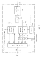
- Fig. 1
- is a block diagram of one possible embodiment of a device for transmitting an optical data signal in accordance with the present invention;
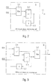
- Fig. 2
- is a block diagram of a possible embodiment of a differential phase shift keying unit included in the device according to the present invention;
- Fig. 3
- is a block diagram of a further embodiment of a differential phase shift keying unit included in the device according to the present invention;
- Fig. 4
- is a block diagram of a further embodiment of a differential phase shift keying unit included in the device according to the present invention;
- Fig. 5
- is a block diagram of a possible embodiment of an amplitude shift keying unit in the device for transmitting an optical data signal according to the present invention;
- Fig. 6
- is a table that is stored in a storage of an amplitude shift keying unit according to
Fig. 5 ; - Fig. 7
- is another table that is stored in a storage of an amplitude shift keying unit according to
Fig. 5 ; - Fig. 8A - 8C
- are constellation diagrams illustrating the operation of the device for transmitting an optical data signal in accordance with the present invention;
- Fig. 9A, 9B
- are diagrams illustrating the operation of the device for transmitting an optical data signal in accordance with the present invention;
- Fig. 10
- is a diagram illustrating the operation of the modulation unit in the device according to the present invention;
- Fig. 11
- is a block diagram of a possible embodiment of a receiver according to the present invention;
- Fig. 12
- is an example of a table that is implemented in the receiver shown in
Fig. 11 ; - Fig. 13
- is an example of a further table that is implemented in the sender shown in
Fig. 5 ; - Fig. 14
- is a signal diagram illustrating the operation of the device for transmitting an optical data signal in accordance with the present invention;
- Fig. 15
- is a further signal diagram illustrating the operation of the device according to the present invention.
- As can be seen in
Fig. 1 , which shows an embodiment of adevice 1 for transmitting an optical data signal in accordance with the present invention, thisdevice 1 comprises asignal input port 2 for receiving a serial data stream having a high data transmission rate. The serial data stream having a high data transmission rate is supplied via aninternal conductor 3 to ademultiplexer 4 that is part of thedevice 1. Thedemultiplexer 4 partitions the serial data stream DS0 having a high data transmission rate into a plurality of data streams DS having a reduced data transmission rate. In the embodiment shown inFig. 1 , thedemultiplexer 4 partitions the serial data stream DS0 having a high data transmission rate into five data streams DS1 - DS5 having a lower data transmission rate. - In the embodiment shown in
Fig. 1 , thesignal input port 1 receives a serial data stream having a high data transmission rate from a data source. This serial data stream is then partitioned by thedemultiplexer 4 into different serial data streams having a reduced data transmission rate. In an alternative embodiment of theinventive device 1 for transmitting an optical data signal, thedevice 1 may receive different serial data streams having a low data transmission rate, in which case this embodiment is not provided with ademultiplexer 4. In one possible embodiment of theinventive device 1, the received serial data stream DS0 having a high data transmission rate has a high data transmission rate of 100 Gbaud. Thedemultiplexer 4 partitions this serial data steam DS0 into several serial data streams DS having a reduced data transmission rate, each having a data transmission rate of e.g. 20 Gbaud. In one possible embodiment of theinventive device 1, the five parallel data streams are subsequently supplied to a 5-fold FEC coding unit for FEC precoding. The embodiment shown inFig. 1 is provided with a coding unit. - In the embodiment shown in
Fig. 1 , two of the serial data streams, that is, the serial data streams DS1 and DS2 are delivered by thedemultiplexer 4 directly to a differential phase shift keying unit 5 (phase difference coding unit). The other three data streams DS3 - DS5 are delivered viacontrollable switches controllable switches control input port 10 of the device 1.The differential phaseshift keying unit 5 performs differential phase shift keying (phase difference coding) of the two serial data streams DS1 and DS2 supplied to it, in order to generate a differential phase shift keying coded data stream. The generated differential phase shift keying coded data stream is output from the differential phaseshift keying unit 5 via aconductor 11. In the illustrated embodiment, the differential phase shift keying coded data stream has a data transmission rate of 40 Gbaud. In the embodiment shown inFig. 1 , two serial data streams DS1 and DS2 are coded by the differential phaseshift keying unit 5 in order to generate a differential phase shift keying coded data stream. In an alternative embodiment, it is also possible to directly modulate a serial data stream with twice the data rate. A partial control signal is generated, with which the downstream modulation unit modulates information in form of a phase difference onto the optical signal. - The amplitude
shift keying unit 9 performs amplitude coding of the other serial data streams DS3, DS4 and DS5, which can be selectively activated, in order to generate an amplitude-coded data stream. This amplitude-coded data stream is output from the amplitudeshift keying device 9 via aconductor 12. In the illustrated embodiment, the generated amplitude-coded data stream has a data transmission rate of 40 Gbaud. The amplitude coding by the amplitudeshift keying unit 9 is based on one data stream, two data streams, or three data streams D3, D4, D5, which can be selectively activated by theswitches internal controller 13 of the device can be set by signal amplifiers included in the amplitudeshift keying unit 9. The control signals for the signal amplifiers are set in accordance with an error rate that thedevice 1 obtains from the receiving side. In one possible embodiment, this error rate, for example the bit error rate (BER), is communicated to theinternal controller 13 of the device via the optical communication channel. In an alternative embodiment, the error rate for the various data streams is communicated to thecontroller 13 via a separate control channel. - A control signal is formed from the differential phase shift keying coded data stream that is output by the differential phase
shift keying unit 5 and the amplitude difference coded data stream that is output by the amplitudedifference coding unit 9. In the embodiment shown inFig. 1 , the differential phase shift keying coded data stream is multiplied by amultiplication unit 14 with the amplitude shift keying coded data stream in order to generate a control signal. The control signal US that is formed by the multiplication of the differential phase shift keying coded data stream with the amplitude shift keying coded data stream is output via aninternal conductor 15 to amodulation unit 16. In one possible embodiment, themodulation unit 16 is a Mach-Zehnder modulator. Themodulation unit 16 generates the optical data signal in dependence of the control signal US that is applied via theconductor 15 and outputs the generated optical data signal via anoptical transmission channel 17. In one possible embodiment, the modulation is effected by driving a symmetric Mach-Zehnder interferometer, which is biased in a zero point, with a hexavalent (six-value) voltage signal. - In the embodiment of the
inventive device 1 as illustrated inFig. 1 , the serial data stream DS0 having a serial data rate of 100 Gbaud is partitioned into five parallel data streams of 20 Gbaud each. Two of these parallel data streams are modulated by differential phase shift keying modulation onto a 40 Gbaud optical signal, whereas the information of the remaining three data streams is transmitted by theamplitude coding device 9 in two consecutive symbols. In order to enable a differential decoding of the phase modulation and thus a more simple decoding of the signal on the receiving side in a delay line interferometer, the two data streams DS1 and DS2 to be coded in-phase are precoded in a preferable embodiment. Since the signals are available at half the symbol rate, in one possible embodiment this precoding can be performed at a low rate. For example, a binary 0 can be coded in a data stream in such a manner that there is no phase change of the optical signal, whereas a binary 1 in the data stream can be coded to a phase change of 180°. This definition is subsequently also observed for the decodingon the receiving side. - The
Figs. 2 - 4 show different embodiments for a differential phaseshift keying unit 5. In the differential phaseshift keying unit 5 illustrated inFig. 2 , the precoding is carried out after the multiplexing, whereas in the embodiments illustrated inFigs. 3 and4 , the precoding is carried out prior to the multiplexing. In the embodiment shown inFig. 2 , the precoding is carried out after multiplexing the two 20 Gbaud data streams to a 40 Gbaud data stream, by feeding back the coded signal and combining it with the signal to be coded in an XOR gate. A multiplexer 5-1 alternatingly puts one of the two applied serial data streams DS1, DS2 through to an output port of the multiplexer. An XOR gate 5-2 downstream from the multiplexer 5-1 comprises a first input port that is connected to the output port of the multiplexer 5-1. An output port of the XOR gate is connected (fed back) via a delay element 5-3 to a second input port of the XOR gate 5-2. The output port of the differential phaseshift keying unit 5 is connected via theconductor 11 with themultiplier 14 illustrated inFig. 1 . -
Fig. 3 shows another embodiment of a differential phaseshift keying unit 5. The differential phaseshift keying unit 5 according toFig. 3 comprises two XOR gates 5-4 and 5-5, whose output ports are connected to a multiplexer 5-6. The output port of the second XOR gate 5-5 is connected via a delay element 5-7 to the second input port of the first XOR gate 5-4. The multiplexer 5-6 switches alternatingly between the two outputs of the two XOR gates 5-4 and 5-5 and outputs a 40 Gbaud differential phase shift keying coded data signal to theconductor 11. -
Fig. 4 illustrates a third example of a differential phaseshift keying unit 5. In the example of a differential phaseshift keying unit 5 shown inFig. 4 , the second XOR gate 5-5 comprises three input ports, the two serial data streams DS1 and DS2 being input to two of those input ports and a signal fed back from the output port of the XOR gate 5-5 via the delay element 5-7 being input to the third of those input ports. The first XOR gate 5-4 receives at its first input port the first serial data stream DS1 and the feedback signal at its second input port. The multiplexer 5-6 switches alternatingly between the two output ports of the two XOR gates and outputs a 40 Gbaud differential phase shift keying coded signal via thesignal conductor 11. - In one possible embodiment of the
inventive device 1, the delay time of the delay elements 5-3 and 5-7 illustrated inFigs. 2, 3 and4 is inversely proportional to the data rate of the serial data streams DS1 and DS2 applied to the input ports. For example, the delay time of the delay element 5-3 shown inFig. 2 may be 25 ps (picoseconds). In the examples shown inFigs. 4 and 5 , the delay time of the delay elements 5-7 may be for example 50 ps. - The remaining three data streams DS3, DS4 and DS5 having 20 Gbaud, respectively, are transmitted by the amplitude shift key coding in two consecutive data symbols. In one possible embodiment, each data symbol receives one of the three possible amplitude values A1, A2 and A3, where A1 < A2 < A3.
- In a preferred embodiment, it is avoided that both symbols take on the value A1, in order to minimize the combination of symbols with the lowest amplitude when decoding the phase signal with a delay line interferometer on the receiver side. In addition, by avoiding this symbol combination, it is possible to attain a criterion for synchronizing the symbol pairs. When the value A1 is decoded in two consecutive symbols, then these are not assigned to a symbol pair.
-
Fig. 6 shows a possible mapping of bit values of the three serial data streams DS3, DS4 and DS5 to the amplitude values in two consecutive symbols. - The amplitude modulation values A1, A2 and A3 listed in the table of
Fig. 6 are generated for example by the circuit shown inFig. 5 from the bit values of the three parallel data streams DS3, DS4 and DS5. The embodiment of the amplitudeshift keying unit 9 shown inFig. 5 includes a storage 9-1 with a readable coding table.Fig. 7 shows the coding table stored in storage 9-1 in one possible embodiment of the amplitudeshift keying unit 9. For each bit combination of the data streams DS3, DS4 and DS5 that are input into the amplitudeshift keying unit 9, a bit combination of the amplitude bits abit1, abit2, abit3 and abit4 is stored. In the embodiment shown inFig. 5 , four bit streams also having 20 Gbaud each are generated from the serial data streams DS3, DS4 and DS5 respectively comprising 3 bit by reading the coding table. The amplitude bits abit1 and abit3 are multiplexed by a first multiplexer 9-2 and the amplitude bits abit2 and abit4 are multiplexed by a second multiplexer 9-3. Thus, two data streams with a data transmission rate of 40 Gbaud each are generated. The two data streams having 40 Gbaud are combined by a NOR gate 9-4 and amplified by a first signal amplifier 9-5. Moreover, the two resulting data streams that are output by the multiplexers 9-2 and 9-3 are each amplified by a signal amplifier 9-6, 9-7, respectively. In one embodiment of theinventive device 1, the signal amplifying factors of the three signal amplifiers 9-5, 9-6 and 9-7 are adjustable. The amplification values of the signal amplifiers 9-5, 9-6 and 9-7 determine the values of the three data levels of the modulated optical signal. In the embodiment shown inFig. 5 , the output signals of the signal amplifiers 9-5, 9-6 and 9-7 are given to an adder 9-8, which adds the three amplified amplitude bits output by the signal amplifiers 9-5, 9-6 and 9-7 to generate the amplitude shift keying coded data stream. The generated amplitude shift keying coded data stream is output via theconductor 12 to themultiplier 14 shown inFig. 1 . - The
Figs. 8A, 8B and 8C illustrate the operation of theinventive device 1 for transmitting an optical data stream. In multi-value modulation methods, more than one information bit is transmitted within one information step or information symbol. The amount of information I that is transmitted per symbol is given by: - I=log2(S), where log2 is the
base 2 logarithm and S is the number of possible symbol states. In QPSK modulation as shown inFig. 8A , the optical signal can take on one of the phase states 0°, 90°, 180° and 270°. Since there are four distinct symbol states S, log2(4)=2 bit are transmitted per symbol. -
Fig. 8B shows a multi-level amplitude modulation method in which the optical signal is transmitted not only with two amplitudes corresponding to thevalues Fig. 8B . -
Fig. 8C shows a constellation diagram that is used with one possible embodiment of theinventive device 1 for transmitting an optical data signal. A combined phase-amplitude modulation is carried out in accordance with the constellation diagram shown inFig. 8C . A three-level amplitude modulation with three amplitude values A1, A2 and A3 is combined with a 180° phase shift keying. The modulation is carried out by driving a symmetricMZ modulation unit 16 that is biased in the zero point, with a hexavalent (six-value) control voltage signal US. In the constellation diagram shown inFig. 8C , the amount of information that is transmitted per symbol is I =log2(6)=2,5 bit. With this, it is possible to achieve a data transmission rate of 100 Gbaud with a symbol rate of < 40 Gbaud. For this, the data stream DS0 having a high data transmission rate of 100 Gbaud is partitioned into for example five parallel data streams DS1 - DS5 with 20 Gbaud each, as in the embodiment shown inFig. 1 . Two parallel data streams DS1 and DS2 are subsequently modulated onto a 40 Gbaud optical data signal by the differential phaseshift keying unit 5, while the information of the remaining three data streams DS3, DS4 and DS5 is transmitted by amplitude modulation in two consecutive data symbols. -
Figs. 9A and 9B illustrate the operation of theinventive device 1.Fig. 9B shows a 3-ASK-PSK modulation constellation diagram for a 40 Gbaud data stream having six different symbol states. - As can be seen in
Fig. 9A , the serial data stream DS0 having a high data transmission rate of for example 100 Gbaud is partitioned into five data streams DS1 - DS5 of 20 Gbaud each. 2.5 bit are transmitted per symbol, in other words, five bits are transmitted in two consecutive symbols. -
Fig. 10 illustrates the principle of the phase/amplitude modulation using a single Mach-Zehnder modulator that is used as amodulation unit 16. The modulation is carried out by driving the symmetric Mach-Zehnder interferometer, which is biased in the zero point, e.g. with a six-value control voltage signal US. Thus, an elaborate nested MZ modulator as needs to be provided for the modulation of QPSK signals is not necessary. -
Fig. 11 shows a circuit diagram of areceiver 18 that receives and decodes the optical data signal that is transmitted over theoptical transmission channel 17. Thereceiver 18 receives the transmitted optical data signal at thesignal input port 19. The received optical signal is split by asplitter 20 to two signal branches. In a first signal branch, the phase modulation (DPSK) of the received optical signal is detected after adelay line interferometer 21, for example with two balanced photodiodes. After clock recovery with a clock recovery unit 22 (CDR: clock and data recovery), the resulting signal is sampled by ademultiplexer 23 and is partitioned into two data streams. The data stream having 40 Gbaud that is recovered after the clock recovery is partitioned by thedemultiplexer 23 into two data streams de1 and de2, which each have a data transmission rate of 20 Gbaud. - In the second signal branch of the
receiver 18, the optical signal that is received by aunit 24 is detected directly by a photodiode. The signal clock is recovered by a subsequentclock recovery unit 25 and the received signal is sampled by a decoding anddemultiplexing unit 26, which has for example two decision thresholds. Preferably, one decision threshold for the first output data stream is situated between the amplitude levels A1 and A2 and the other decision threshold for the other output data stream is situated between the amplitude levels A2 and A3. The decoding anddemultiplexing unit 26 generates three further output data streams de3, de4 and de5. The generated five serial data streams de1, de2, de3, de4 and de5 are supplied to an FEC (forward error correction)unit 27, which determines the attained error rate or bit error rate (BER) for each of the five received serial data streams de1 - de5. The error rates or BERs that are determined in this manner are provided over a separate channel to theinternal controller 13 of thedevice 1 for transmitting an optical data signal, as shown inFig. 1 . In one possible embodiment, theinternal controller 13 can adjust the signal amplification factors of the signal amplifiers included in the amplitudeshift keying unit 9 with the aid of these error rates. -
Fig. 12 shows a table that is stored within a storage of the decoding anddemultiplexing unit 26. - If the received signal is smaller than a lower decision threshold (that is, level 1), then the deciders in the decoding and
demultiplexing unit 26 generate a logical 0 for both data streams. If the received signal is between the two decision thresholds, then the data stream A1 is decided to be logical 1 and the data stream A2 is decided as logical 0. If the received signal is above the two decision thresholds (that is, at level 3), then both data streams receive a logical 1. These decisions are made for both coded symbols. The resulting signal level is then determined with a numerical approach from the data A1 and A2 of a symbol: signal level = A1 + A2 + 1. - The resulting output data streams de3, de4 and de5 are determined using the decoding table shown in
Fig. 12 . - In one possible embodiment, the control of the amplification factors of the signal amplifiers 9-5, 9-6 and 9-7 of the amplitude
shift keying unit 9 shown inFig. 5 is carried out in accordance with the bit error rates BER1, BER2, BER3, BER4 and BER5, that are determined by theFEC unit 27, as follows: - If (BER1+BER2)/2>BER3, then the signal amplification factor of the signal amplifier 9-5 is increased.
- If (BER1+BER2)/2<BER3, then the signal amplification factor of the signal amplifier 9-5 is reduced.
- If BER3>BER5, then the signal amplification factor of the second signal amplifier 9-6 is increased.
- If BER3<BER5, then the signal amplification factor of the second signal amplifier 9-6 is recuded.
- In this embodiment, the signal amplification factor of the third signal amplifier 9-7 stays constant. The adder 9-8 of the amplitude
shift keying unit 9 outputs a ternary (having three values) data stream having a data transmission rate of 40 Gbaud. - In one possible embodiment of the inventive method for data transmission of an optical data signal, the transmission behaviour of the ASK-DPSK modulation method is optimized. In one possible embodiment, the decision threshold is shifted in such a mannter that the error rate of the received signal is minimized. The error rate or bit error rate can be determined by evaluating an FEC algorithm with the
FEC unit 27. In an alternative embodiment, certain overhead bytes or header data of a packet data transmission can be evaluated in order to determine the error rate or bit error rate BER. - In the
inventive device 1, for example three independent decision thresholds are optimized. In order to receive an unambiguous error signal for the feedback for optimizing the decision threshold, in other words, an error signal that depends only on the setting of a single decision threshold and that stays nearly constant when changing the other two decision thresholds, it is possible to use a predetermined coding algorithm. - In an alternative embodiment, to optimize the transmission behaviour of the 3-ASK-DPSK modulation method, the modulation levels are changed until an optimal error rate is set. The change of the modulation levels influences all transmitted data. For example, a reduction of the lowermost level leads to an increase of the error rate of the DPSK coded data component, whereas the error rate of the 3-ASK coded signal component is improved. A change of the middle modulation level, on the other hand, does not lead to a change of the DPSK error rate, however, the error rate of the 3-ASK data component is changed depending on the coding algorithm. In one possible embodiment, a coding algorithm is used, that enables a differentiation of the resulting errors in an upper and in a lower eye of the 3-ASK signal.
- In case of a combined optimization of the decision threshold and the modulation level, the optimization of the decision threshold is preferably carried out faster than the change of the modulation levels, so that in case of a change of the modulation levels the received signal is first error optimized by adjusting the decision threshold, before making a conclusion about the influence of the change of the modulation level. Thus, it can be prevented that the control algorithm becomes instable.
-
Fig. 13 shows a table listing an optimized coding of the ASK component of thedevice 1. In this embodiment, the ASK signal component is code in such a manner that in case of an error in the decision between the lower and the middle modulation level or in the decision between the middle and the upper modulation level, at least one of the respective coded bits of a symbol pair stays unaffected. The table inFig. 13 shows an optimized coding rule, wherein three data bits are respectively coded into two three-level (or ternary) symbols. - For the decoding of the received signal on the receiving side with the
receiver 18 shown inFig. 11 , two decisions are made for each symbol. One decision threshold is located for the first output data stream between thelevels levels Fig. 13 are generated for the data streams. - When the decision thresholds are not set optimally, or when the signal distance is too low between the two levels, then in one possible embodiment, the signal levels can be recognized as being incorrect. In this case, there may be an incorrect decision between the
levels levels - The coding of the ASK signal component shown in
Fig. 13 is chosen in one embodiment such that the first case of an incorrect decision between thelevels levels -
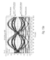
Figs. 14A and14B show the eye diagrams of a DPSK modulated signal and of an ASK modulated signal.Fig. 14A shows the eye diagram of a DPSK signal after DLI decoding. The upper part of the diagram corresponds to a 180° phase difference of the optical signal. -
Fig. 14B shows the eye diagram of a 3-ASK signal. Here, the amplitude is modulated between three signal levels (level 1,level 2 and level 3). -
Fig. 14C shows a corresponding DPSK-3-ASK constellation diagram. Here, the amplitude is modulated between three signal levels and there is a 180° phase difference. -
Figs. 15A ,15B and 15C show eye diagrams for DPSK-2-ASK modulation methods and a corresponding eye diagram.Fig. 15A shows an eye diagram of a DPSK signal after DLI decoding. The upper portion of the eye diagram indicates a 180° phase difference of the optical signal and the negative portion of the constellation diagram shown inFig. 15C . - Compared to
Fig. 14A , the eye distance in the middle ofFig. 15A is larger for the DPSK decision. The fact that this eye distance is larger than for the DPSK-3-ASK graph as shown inFig. 14A affords an additional margin (of about 4 dB) for signal interferences while lowering the aggregated data transmission rate from 100 Gbaud to 80 Gbaud. -
Fig. 15B shows an eye diagram for a 2-ASK signal. The amplitude of the signal is modulated between two levels (level 2 and level 3), which means that thelevel 1 shown inFig.14A is eliminated. -
Fig. 15C shows the corresponding DPSK-2-ASK constellation diagram. The amplitude is modulated between two levels and can cause a relative phase shift of 180° between two values. Here,level 2 is shifted by one bit towards the point of origin of the coordinate system, in order to provide a better performance, which is attained due to the larger separation between the symbols. - With the
inventive device 1, data information having a high information rate can be modulated onto an optical carrier using electrooptical comoponents, that is, amplifiers, modulators and photodiodes with a bandwidth of about 30-40% of the information rate. - The
inventive device 1 and the inventive method combine amplitude and phase modulation, transmitting for example six possible symbol states in one symbol. The modulation can be performed with a single Mach-Zehnder modulator. Even when using component parts with a relatively low frequency bandwidth, it is possible to attain a very high data transmission rate with theinventive device 1 or the inventive method. - If the number of amplitude levels is reduced for example from 3 to 2 and the corresponding coding/decoding scheme is modified accordingly, then the entire channel capacity can be reduced to a transmission rate of 80 Gb/s, so that noise or other signal interferences of about 4 decibel can be compensated.
Claims (15)
- A device (1) for transmitting an optical data signal over an optical transmission channel (17), the device comprising:(a) a differential phase shift keying unit (5) for differential phase shift key coding of at least one serial data stream (DS1, DS2) to generate a differential phase shift keying coded data stream;(b) an amplitude shift keying unit (9) for amplitude shift key coding of at least two further serial data streams (DS1, DS2, DS3) that can be selectively activated with controllable switches (6, 7, 8) to generate an amplitude shift keying coded data stream, wherein the switches (6, 7, 8) are controlled in accordance with an operation mode control signal;(c) a modulation unit (16) for generating an optical data signal in accordance with a control signal (US) that is formed from the generated differential phase shift keying coded data stream and from the generated amplitude shift keying coded data stream.
- The device according to claim 1,
wherein the modulation unit (16) is a Mach-Zehnder modulator. - The device according to claim 1 or 2,
wherein a multiplication unit (14) forms the control signal (US) for the modulation unit (16) by multiplication of the differential phase shift keying coded data stream with the amplitude shift keying coded data stream. - The device according to any of claims claim 1 to 3,
wherein a demultiplexer (4) partitions a serial data stream (DSO) having a high data transmission rate into a plurality of serial data streams (DS1, DS2, DS3, DS4, DS5) having a reduced data transmission rate. - The device according to claim 4,
wherein two of the serial data streams (DS1, DS2) having a reduced data transmission rate are output by the demultiplexer (4) to the differential phase shift keying unit (5). - The device according to claim 5,
wherein the other serial data streams (DS3, DS4, DS5) having a reduced data transmission rate are output by the demultiplexer (4) to the amplitude shift keying unit (9). - The device according to claim 6,
wherein the serial data streams having a reduced transmission rate that are output to the amplitude shift keying unit (9) can be respectively selectively activated by the controllable switches (6, 7, 8). - The device according to any of claims 1 to 7,
wherein the differential phase shift keying unit (5) comprises:- a multiplexer (5-1) that switches alternatingly between two serial data streams (DS1, DS2) and outputs a data stream at an output port of the multiplexer (5-1);- an XOR gate (5-2) arranged downstream from the multiplexer, the XOR gate (5-2) having a first input port that is connected to the output port of the multiplexer (5-1) and a second input port that is connected via a delay element (5-3) to an output port of the XOR gate (5-2). - The device according to any of claims 1 to 7,
wherein the differential phase shift keying unit (5) comprises a first XOR gate (5-4) receiving a serial data stream at a first input port and receiving at a second input port an output signal that is fed back from an output port of a second XOR gate (5-5) via a delay element (5-7), and a multiplexer (5-6) arranged downstream of the XOR gates (5-4, 5-5) that switches alternatingly between the output ports of the two XOR gates (5-4, 5-5). - The device according to claim 9,
wherein the delay time of the delay element (5-7) is inversely proportional to the data rate of the serial data stream at the input ports of the XOR gate (5-4, 5-5). - The device according to any of claims 1 to 10,
wherein the amplitude shift keying unit (9) comprises:(a) a storage (9-1) for storing a coding table that can be read out, in which a bit combination (abit1, abit2, abit3, abit4) of amplitude bits is stored for any bit combination of the serial data streams (DS1, DS2, DS3) input into the amplitude shift keying unit (9);(b) a multiplexer (9-2, 9-3) for multiplexing the amplitude bits that are read out from the storage (9-1);(c) amplifiers (9-5, 9-6, 9-7) with adjustable amplification factors for amplifying the multiplexed amplitude bits; and(d) an adder (9-8) that adds amplified amplitude bits output by the amplifiers (9-5, 9-6, 9-7) to generate the amplitude shift keying coded data stream. - The device according to claim 11,
wherein amplification factors of the amplifiers (9-5, 9-6, 9-7) in the amplitude shift keying unit (9) are adjusted by a controller (13) in accordance with a detected error rate that occurs when transmitting the optical data signal over the optical transmission channel to a receiver (18). - The device according to claim 12,
wherein the detected error rate is transmitted from the receiver (18) over a communication channel to the controller (13). - The device according to any of claims 4 to 7,
wherein the serial data stream (DSO) having a high data transmission rate has a data transmission rate of 100 Gbaud;
wherein the serial data streams (DS1, DS2, DS3, DS4, DS5) having a reduced data transmision rate each have a data transmission rate of 20 Gbaud; and
wherein the generated differential phase shift keying coded data stream and the generated amplitude shift keying coded data stream each have a data transmission rate of 40 Gbaud. - A method for transmitting an optical data signal over an optical transmission channel, the method comprising the following steps:(a) forming a differential phase shift keying coded data stream from serial data streams (DS1, DS2);(b) forming an amplitude shift keying coded data stream from further serial data streams (DS3, DS4, DS5), wherein the further serial data streams (DS3, DS4, DS5) are selectively activated in accordance with an operation mode control signal;(c) generating the optical data signal with a modulation unit (16) in accordance with a control signal (US) that is formed from the differential phase shift keying coded data stream and the amplitude shift keying coded data stream.
Applications Claiming Priority (1)
| Application Number | Priority Date | Filing Date | Title |
|---|---|---|---|
| DE102008017644A DE102008017644A1 (en) | 2008-04-04 | 2008-04-04 | Apparatus and method for transmitting an optical data signal |
Publications (2)
| Publication Number | Publication Date |
|---|---|
| EP2107702A1 true EP2107702A1 (en) | 2009-10-07 |
| EP2107702B1 EP2107702B1 (en) | 2014-01-01 |
Family
ID=40887015
Family Applications (1)
| Application Number | Title | Priority Date | Filing Date |
|---|---|---|---|
| EP09157267.7A Not-in-force EP2107702B1 (en) | 2008-04-04 | 2009-04-03 | Device and method for transmitting optical data signals |
Country Status (3)
| Country | Link |
|---|---|
| US (1) | US8326158B2 (en) |
| EP (1) | EP2107702B1 (en) |
| DE (1) | DE102008017644A1 (en) |
Families Citing this family (7)
| Publication number | Priority date | Publication date | Assignee | Title |
|---|---|---|---|---|
| US9130679B1 (en) * | 2011-05-27 | 2015-09-08 | Nec Laboratories America, Inc. | Polarization-switched differential ternary phase-shift keying |
| KR102233039B1 (en) * | 2013-10-29 | 2021-03-30 | 삼성전자주식회사 | A method and system using ternary sequences for simultaneous transmission to coherent and non-coherent recievers |
| US9584260B2 (en) * | 2014-03-06 | 2017-02-28 | Cisco Technology, Inc. | Optimization of optical transmission capacity |
| JP6755676B2 (en) * | 2016-03-02 | 2020-09-16 | 日本ルメンタム株式会社 | Optical transmission module |
| EP3404856B1 (en) * | 2017-05-15 | 2024-04-10 | Nokia Solutions and Networks Oy | Method of and apparatus for modulating an optical carrier |
| US11736320B2 (en) * | 2022-02-14 | 2023-08-22 | Ultralogic 6G, Llc | Multiplexed amplitude-phase modulation for 5G/6G noise mitigation |
| US12250100B2 (en) * | 2022-02-14 | 2025-03-11 | David E. Newman | Selecting a modulation scheme responsive to fault types in 5G/6G |
Citations (2)
| Publication number | Priority date | Publication date | Assignee | Title |
|---|---|---|---|---|
| JPH11136206A (en) * | 1997-10-24 | 1999-05-21 | Matsushita Electric Ind Co Ltd | Data transmission equipment |
| US20080031630A1 (en) * | 2006-08-01 | 2008-02-07 | Tomoaki Ohira | Optical transmitter and optical transmission system |
Family Cites Families (9)
| Publication number | Priority date | Publication date | Assignee | Title |
|---|---|---|---|---|
| CA2104753C (en) * | 1992-10-29 | 1999-02-16 | Kotikalapudi Sriram | Bandwidth allocation, transmission scheduling, and congestion avoidance in broadband atm networks |
| US5481542A (en) * | 1993-11-10 | 1996-01-02 | Scientific-Atlanta, Inc. | Interactive information services control system |
| US6556326B2 (en) * | 1996-12-20 | 2003-04-29 | Tyco Telecommunications (Us) Inc. | Synchronous amplitude modulation for improved performance of optical transmission systems |
| US7085500B2 (en) * | 2001-04-30 | 2006-08-01 | Lockheed Martin Corp. | Programmable optical vector modulator and method for use in coherent optical communications |
| US7019882B1 (en) * | 2002-03-21 | 2006-03-28 | Lockheed Martin Corporation | Generation of M-ary digital signaling constellations directly at lightwave frequencies |
| US20030198478A1 (en) * | 2002-04-23 | 2003-10-23 | Quellan, Inc. | Method and system for generating and decoding a bandwidth efficient multi-level signal |
| US7340168B2 (en) * | 2003-09-29 | 2008-03-04 | Lucent Technologies Inc. | System and method for optically labeled packet transmission |
| US7349636B2 (en) * | 2003-12-11 | 2008-03-25 | Mario Zitelli | Optical phase and intensity modulation with improved transmitters |
| US7804761B2 (en) * | 2007-05-09 | 2010-09-28 | Ceragon Networks Ltd. | Multiplexing separately modulated channels |
-
2008
- 2008-04-04 DE DE102008017644A patent/DE102008017644A1/en not_active Withdrawn
-
2009
- 2009-04-03 US US12/384,465 patent/US8326158B2/en not_active Expired - Fee Related
- 2009-04-03 EP EP09157267.7A patent/EP2107702B1/en not_active Not-in-force
Patent Citations (2)
| Publication number | Priority date | Publication date | Assignee | Title |
|---|---|---|---|---|
| JPH11136206A (en) * | 1997-10-24 | 1999-05-21 | Matsushita Electric Ind Co Ltd | Data transmission equipment |
| US20080031630A1 (en) * | 2006-08-01 | 2008-02-07 | Tomoaki Ohira | Optical transmitter and optical transmission system |
Also Published As
| Publication number | Publication date |
|---|---|
| US8326158B2 (en) | 2012-12-04 |
| US20090252501A1 (en) | 2009-10-08 |
| DE102008017644A1 (en) | 2009-10-15 |
| EP2107702B1 (en) | 2014-01-01 |
Similar Documents
| Publication | Publication Date | Title |
|---|---|---|
| EP2107702B1 (en) | Device and method for transmitting optical data signals | |
| US10735135B2 (en) | Variable spectral efficiency optical modulation schemes | |
| US9331788B2 (en) | Communication device and communication method | |
| CA2658148C (en) | A receiver structure and method for the demodulation of a quadrature-modulated signal | |
| US11025405B2 (en) | High capacity optical data transmission using intensity-modulation and direct-detection | |
| US20060269294A1 (en) | Optical transmission equipment and integrated circuit | |
| JP5213991B2 (en) | Method and apparatus for generation and detection of optical difference variable multilevel phase shift keying (ODVMPSK / PAM) signal by pulse amplitude modulation | |
| EP2251999B1 (en) | Data transmission method and network for transmitting a digital optical signal over optical transmission links and networks | |
| US9306780B2 (en) | Optical transmission for binary and duobinary modulation formats | |
| US20190199443A1 (en) | Trellis Based Processing for Robust Digital Multiband Transmission | |
| US10749727B2 (en) | Method for protecting a link in an optical network | |
| BR102012005220B1 (en) | method for encoding digital data for transmission over a plastic optical fiber, method for receiving and decoding a digital signal encoded by an encoding method, apparatus for receiving and decoding a digital signal encoded with an apparatus and integrated circuit | |
| US9806804B2 (en) | Method and apparatus for configuring an optical path | |
| US20080056727A1 (en) | Optical transmitter and drive method of same | |
| CN102577177A (en) | Multi-value modulated light transmitting and receiving device and multi-value modulated light transmitting and receiving method | |
| US7603044B1 (en) | Polarization control for multichannel and polarization multiplexed optical transport networks | |
| EP2168278B1 (en) | A method and apparatus for increasing the capacity of a data communication channel | |
| EP3028394A1 (en) | Parameter control for optical multicarrier signal | |
| EP1708391A1 (en) | Method and apparatus for improving dual-polarization optical communication performance | |
| EP2843854A1 (en) | Method, transmitter and receiver device for transmitting a binary digital transmit signal over an optical transmission link | |
| JP4927617B2 (en) | Data transmission apparatus and transmission code generation method | |
| JPWO2018123717A1 (en) | Receiver, transmitter, optical communication system, and optical communication method | |
| EP1318639B1 (en) | Digital transmission system with receiver using parallel decision circuits | |
| US20090220249A1 (en) | Demodulation circuit | |
| EP2571217A1 (en) | Method for transmitting optical signal with adaptive bitrate using a PDM-QAM modulation scheme and a corresponding transmitter |
Legal Events
| Date | Code | Title | Description |
|---|---|---|---|
| PUAI | Public reference made under article 153(3) epc to a published international application that has entered the european phase |
Free format text: ORIGINAL CODE: 0009012 |
|
| AK | Designated contracting states |
Kind code of ref document: A1 Designated state(s): AT BE BG CH CY CZ DE DK EE ES FI FR GB GR HR HU IE IS IT LI LT LU LV MC MK MT NL NO PL PT RO SE SI SK TR |
|
| 17P | Request for examination filed |
Effective date: 20091211 |
|
| RAP1 | Party data changed (applicant data changed or rights of an application transferred) |
Owner name: ADVA OPTICAL NETWORKING SE |
|
| REG | Reference to a national code |
Ref country code: DE Ref legal event code: R079 Ref document number: 602009021101 Country of ref document: DE Free format text: PREVIOUS MAIN CLASS: H04B0010155000 Ipc: H04B0010516000 |
|
| RIC1 | Information provided on ipc code assigned before grant |
Ipc: H04B 10/556 20130101ALI20130807BHEP Ipc: H04B 10/54 20130101ALI20130807BHEP Ipc: H04B 10/516 20130101AFI20130807BHEP Ipc: H04B 10/50 20130101ALI20130807BHEP |
|
| GRAP | Despatch of communication of intention to grant a patent |
Free format text: ORIGINAL CODE: EPIDOSNIGR1 |
|
| INTG | Intention to grant announced |
Effective date: 20130920 |
|
| GRAS | Grant fee paid |
Free format text: ORIGINAL CODE: EPIDOSNIGR3 |
|
| GRAA | (expected) grant |
Free format text: ORIGINAL CODE: 0009210 |
|
| AK | Designated contracting states |
Kind code of ref document: B1 Designated state(s): AT BE BG CH CY CZ DE DK EE ES FI FR GB GR HR HU IE IS IT LI LT LU LV MC MK MT NL NO PL PT RO SE SI SK TR |
|
| REG | Reference to a national code |
Ref country code: GB Ref legal event code: FG4D |
|
| REG | Reference to a national code |
Ref country code: CH Ref legal event code: EP |
|
| REG | Reference to a national code |
Ref country code: IE Ref legal event code: FG4D |
|
| REG | Reference to a national code |
Ref country code: AT Ref legal event code: REF Ref document number: 647991 Country of ref document: AT Kind code of ref document: T Effective date: 20140215 |
|
| REG | Reference to a national code |
Ref country code: DE Ref legal event code: R096 Ref document number: 602009021101 Country of ref document: DE Effective date: 20140220 |
|
| REG | Reference to a national code |
Ref country code: NL Ref legal event code: VDEP Effective date: 20140101 |
|
| REG | Reference to a national code |
Ref country code: AT Ref legal event code: MK05 Ref document number: 647991 Country of ref document: AT Kind code of ref document: T Effective date: 20140101 |
|
| REG | Reference to a national code |
Ref country code: LT Ref legal event code: MG4D |
|
| PG25 | Lapsed in a contracting state [announced via postgrant information from national office to epo] |
Ref country code: IS Free format text: LAPSE BECAUSE OF FAILURE TO SUBMIT A TRANSLATION OF THE DESCRIPTION OR TO PAY THE FEE WITHIN THE PRESCRIBED TIME-LIMIT Effective date: 20140501 Ref country code: LT Free format text: LAPSE BECAUSE OF FAILURE TO SUBMIT A TRANSLATION OF THE DESCRIPTION OR TO PAY THE FEE WITHIN THE PRESCRIBED TIME-LIMIT Effective date: 20140101 |
|
| PG25 | Lapsed in a contracting state [announced via postgrant information from national office to epo] |
Ref country code: FI Free format text: LAPSE BECAUSE OF FAILURE TO SUBMIT A TRANSLATION OF THE DESCRIPTION OR TO PAY THE FEE WITHIN THE PRESCRIBED TIME-LIMIT Effective date: 20140101 Ref country code: SE Free format text: LAPSE BECAUSE OF FAILURE TO SUBMIT A TRANSLATION OF THE DESCRIPTION OR TO PAY THE FEE WITHIN THE PRESCRIBED TIME-LIMIT Effective date: 20140101 Ref country code: CY Free format text: LAPSE BECAUSE OF FAILURE TO SUBMIT A TRANSLATION OF THE DESCRIPTION OR TO PAY THE FEE WITHIN THE PRESCRIBED TIME-LIMIT Effective date: 20140101 Ref country code: NL Free format text: LAPSE BECAUSE OF FAILURE TO SUBMIT A TRANSLATION OF THE DESCRIPTION OR TO PAY THE FEE WITHIN THE PRESCRIBED TIME-LIMIT Effective date: 20140101 Ref country code: ES Free format text: LAPSE BECAUSE OF FAILURE TO SUBMIT A TRANSLATION OF THE DESCRIPTION OR TO PAY THE FEE WITHIN THE PRESCRIBED TIME-LIMIT Effective date: 20140101 Ref country code: PT Free format text: LAPSE BECAUSE OF FAILURE TO SUBMIT A TRANSLATION OF THE DESCRIPTION OR TO PAY THE FEE WITHIN THE PRESCRIBED TIME-LIMIT Effective date: 20140502 Ref country code: AT Free format text: LAPSE BECAUSE OF FAILURE TO SUBMIT A TRANSLATION OF THE DESCRIPTION OR TO PAY THE FEE WITHIN THE PRESCRIBED TIME-LIMIT Effective date: 20140101 |
|
| PG25 | Lapsed in a contracting state [announced via postgrant information from national office to epo] |
Ref country code: HR Free format text: LAPSE BECAUSE OF FAILURE TO SUBMIT A TRANSLATION OF THE DESCRIPTION OR TO PAY THE FEE WITHIN THE PRESCRIBED TIME-LIMIT Effective date: 20140101 Ref country code: BE Free format text: LAPSE BECAUSE OF FAILURE TO SUBMIT A TRANSLATION OF THE DESCRIPTION OR TO PAY THE FEE WITHIN THE PRESCRIBED TIME-LIMIT Effective date: 20140101 Ref country code: LV Free format text: LAPSE BECAUSE OF FAILURE TO SUBMIT A TRANSLATION OF THE DESCRIPTION OR TO PAY THE FEE WITHIN THE PRESCRIBED TIME-LIMIT Effective date: 20140101 |
|
| REG | Reference to a national code |
Ref country code: DE Ref legal event code: R097 Ref document number: 602009021101 Country of ref document: DE |
|
| PG25 | Lapsed in a contracting state [announced via postgrant information from national office to epo] |
Ref country code: RO Free format text: LAPSE BECAUSE OF FAILURE TO SUBMIT A TRANSLATION OF THE DESCRIPTION OR TO PAY THE FEE WITHIN THE PRESCRIBED TIME-LIMIT Effective date: 20140101 Ref country code: CZ Free format text: LAPSE BECAUSE OF FAILURE TO SUBMIT A TRANSLATION OF THE DESCRIPTION OR TO PAY THE FEE WITHIN THE PRESCRIBED TIME-LIMIT Effective date: 20140101 Ref country code: EE Free format text: LAPSE BECAUSE OF FAILURE TO SUBMIT A TRANSLATION OF THE DESCRIPTION OR TO PAY THE FEE WITHIN THE PRESCRIBED TIME-LIMIT Effective date: 20140101 Ref country code: DK Free format text: LAPSE BECAUSE OF FAILURE TO SUBMIT A TRANSLATION OF THE DESCRIPTION OR TO PAY THE FEE WITHIN THE PRESCRIBED TIME-LIMIT Effective date: 20140101 |
|
| PLBE | No opposition filed within time limit |
Free format text: ORIGINAL CODE: 0009261 |
|
| STAA | Information on the status of an ep patent application or granted ep patent |
Free format text: STATUS: NO OPPOSITION FILED WITHIN TIME LIMIT |
|
| PG25 | Lapsed in a contracting state [announced via postgrant information from national office to epo] |
Ref country code: LU Free format text: LAPSE BECAUSE OF FAILURE TO SUBMIT A TRANSLATION OF THE DESCRIPTION OR TO PAY THE FEE WITHIN THE PRESCRIBED TIME-LIMIT Effective date: 20140403 Ref country code: MC Free format text: LAPSE BECAUSE OF FAILURE TO SUBMIT A TRANSLATION OF THE DESCRIPTION OR TO PAY THE FEE WITHIN THE PRESCRIBED TIME-LIMIT Effective date: 20140101 Ref country code: PL Free format text: LAPSE BECAUSE OF FAILURE TO SUBMIT A TRANSLATION OF THE DESCRIPTION OR TO PAY THE FEE WITHIN THE PRESCRIBED TIME-LIMIT Effective date: 20140101 Ref country code: SK Free format text: LAPSE BECAUSE OF FAILURE TO SUBMIT A TRANSLATION OF THE DESCRIPTION OR TO PAY THE FEE WITHIN THE PRESCRIBED TIME-LIMIT Effective date: 20140101 |
|
| REG | Reference to a national code |
Ref country code: CH Ref legal event code: PL |
|
| 26N | No opposition filed |
Effective date: 20141002 |
|
| REG | Reference to a national code |
Ref country code: DE Ref legal event code: R097 Ref document number: 602009021101 Country of ref document: DE Effective date: 20141002 |
|
| REG | Reference to a national code |
Ref country code: FR Ref legal event code: ST Effective date: 20141231 |
|
| REG | Reference to a national code |
Ref country code: IE Ref legal event code: MM4A |
|
| PG25 | Lapsed in a contracting state [announced via postgrant information from national office to epo] |
Ref country code: CH Free format text: LAPSE BECAUSE OF NON-PAYMENT OF DUE FEES Effective date: 20140430 Ref country code: LI Free format text: LAPSE BECAUSE OF NON-PAYMENT OF DUE FEES Effective date: 20140430 |
|
| PG25 | Lapsed in a contracting state [announced via postgrant information from national office to epo] |
Ref country code: FR Free format text: LAPSE BECAUSE OF NON-PAYMENT OF DUE FEES Effective date: 20140430 |
|
| PG25 | Lapsed in a contracting state [announced via postgrant information from national office to epo] |
Ref country code: IE Free format text: LAPSE BECAUSE OF NON-PAYMENT OF DUE FEES Effective date: 20140403 |
|
| PG25 | Lapsed in a contracting state [announced via postgrant information from national office to epo] |
Ref country code: SI Free format text: LAPSE BECAUSE OF FAILURE TO SUBMIT A TRANSLATION OF THE DESCRIPTION OR TO PAY THE FEE WITHIN THE PRESCRIBED TIME-LIMIT Effective date: 20140101 |
|
| PG25 | Lapsed in a contracting state [announced via postgrant information from national office to epo] |
Ref country code: MT Free format text: LAPSE BECAUSE OF FAILURE TO SUBMIT A TRANSLATION OF THE DESCRIPTION OR TO PAY THE FEE WITHIN THE PRESCRIBED TIME-LIMIT Effective date: 20140101 |
|
| PG25 | Lapsed in a contracting state [announced via postgrant information from national office to epo] |
Ref country code: NO Free format text: LAPSE BECAUSE OF FAILURE TO SUBMIT A TRANSLATION OF THE DESCRIPTION OR TO PAY THE FEE WITHIN THE PRESCRIBED TIME-LIMIT Effective date: 20140401 |
|
| PG25 | Lapsed in a contracting state [announced via postgrant information from national office to epo] |
Ref country code: BG Free format text: LAPSE BECAUSE OF FAILURE TO SUBMIT A TRANSLATION OF THE DESCRIPTION OR TO PAY THE FEE WITHIN THE PRESCRIBED TIME-LIMIT Effective date: 20140101 Ref country code: GR Free format text: LAPSE BECAUSE OF FAILURE TO SUBMIT A TRANSLATION OF THE DESCRIPTION OR TO PAY THE FEE WITHIN THE PRESCRIBED TIME-LIMIT Effective date: 20140402 Ref country code: IT Free format text: LAPSE BECAUSE OF FAILURE TO SUBMIT A TRANSLATION OF THE DESCRIPTION OR TO PAY THE FEE WITHIN THE PRESCRIBED TIME-LIMIT Effective date: 20140101 |
|
| PG25 | Lapsed in a contracting state [announced via postgrant information from national office to epo] |
Ref country code: HU Free format text: LAPSE BECAUSE OF FAILURE TO SUBMIT A TRANSLATION OF THE DESCRIPTION OR TO PAY THE FEE WITHIN THE PRESCRIBED TIME-LIMIT; INVALID AB INITIO Effective date: 20090403 Ref country code: TR Free format text: LAPSE BECAUSE OF FAILURE TO SUBMIT A TRANSLATION OF THE DESCRIPTION OR TO PAY THE FEE WITHIN THE PRESCRIBED TIME-LIMIT Effective date: 20140101 |
|
| PG25 | Lapsed in a contracting state [announced via postgrant information from national office to epo] |
Ref country code: MK Free format text: LAPSE BECAUSE OF FAILURE TO SUBMIT A TRANSLATION OF THE DESCRIPTION OR TO PAY THE FEE WITHIN THE PRESCRIBED TIME-LIMIT Effective date: 20140101 |
|
| PGFP | Annual fee paid to national office [announced via postgrant information from national office to epo] |
Ref country code: DE Payment date: 20200430 Year of fee payment: 12 |
|
| PGFP | Annual fee paid to national office [announced via postgrant information from national office to epo] |
Ref country code: GB Payment date: 20200427 Year of fee payment: 12 |
|
| REG | Reference to a national code |
Ref country code: DE Ref legal event code: R119 Ref document number: 602009021101 Country of ref document: DE |
|
| GBPC | Gb: european patent ceased through non-payment of renewal fee |
Effective date: 20210403 |
|
| PG25 | Lapsed in a contracting state [announced via postgrant information from national office to epo] |
Ref country code: GB Free format text: LAPSE BECAUSE OF NON-PAYMENT OF DUE FEES Effective date: 20210403 Ref country code: DE Free format text: LAPSE BECAUSE OF NON-PAYMENT OF DUE FEES Effective date: 20211103 |