EP2107041A2 - Mold having nanometric features, method for realising such a mold and corresponding use of it in a method for realising an array of carbon nanotubes - Google Patents
Mold having nanometric features, method for realising such a mold and corresponding use of it in a method for realising an array of carbon nanotubes Download PDFInfo
- Publication number
- EP2107041A2 EP2107041A2 EP09156999A EP09156999A EP2107041A2 EP 2107041 A2 EP2107041 A2 EP 2107041A2 EP 09156999 A EP09156999 A EP 09156999A EP 09156999 A EP09156999 A EP 09156999A EP 2107041 A2 EP2107041 A2 EP 2107041A2
- Authority
- EP
- European Patent Office
- Prior art keywords
- projections
- layer
- mold
- substrate
- preset
- Prior art date
- Legal status (The legal status is an assumption and is not a legal conclusion. Google has not performed a legal analysis and makes no representation as to the accuracy of the status listed.)
- Withdrawn
Links
- 238000000034 method Methods 0.000 title claims abstract description 116
- OKTJSMMVPCPJKN-UHFFFAOYSA-N Carbon Chemical compound [C] OKTJSMMVPCPJKN-UHFFFAOYSA-N 0.000 title claims abstract description 87
- 239000002041 carbon nanotube Substances 0.000 title claims abstract description 86
- 229910021393 carbon nanotube Inorganic materials 0.000 title claims abstract description 86
- 239000000758 substrate Substances 0.000 claims abstract description 133
- 239000000463 material Substances 0.000 claims abstract description 37
- 239000002071 nanotube Substances 0.000 claims description 77
- 239000002105 nanoparticle Substances 0.000 claims description 64
- XUIMIQQOPSSXEZ-UHFFFAOYSA-N Silicon Chemical compound [Si] XUIMIQQOPSSXEZ-UHFFFAOYSA-N 0.000 claims description 51
- 229910052710 silicon Inorganic materials 0.000 claims description 51
- 239000010703 silicon Substances 0.000 claims description 51
- 230000003197 catalytic effect Effects 0.000 claims description 45
- 229920000642 polymer Polymers 0.000 claims description 35
- 238000000151 deposition Methods 0.000 claims description 25
- 238000005530 etching Methods 0.000 claims description 23
- 239000006185 dispersion Substances 0.000 claims description 20
- 229910052751 metal Inorganic materials 0.000 claims description 15
- 239000002184 metal Substances 0.000 claims description 15
- 230000003647 oxidation Effects 0.000 claims description 15
- 238000007254 oxidation reaction Methods 0.000 claims description 15
- 238000009736 wetting Methods 0.000 claims description 13
- 230000005499 meniscus Effects 0.000 claims description 12
- 230000008021 deposition Effects 0.000 claims description 11
- XLYOFNOQVPJJNP-UHFFFAOYSA-N water Substances O XLYOFNOQVPJJNP-UHFFFAOYSA-N 0.000 claims description 11
- 230000005684 electric field Effects 0.000 claims description 9
- 238000007306 functionalization reaction Methods 0.000 claims description 8
- 230000015572 biosynthetic process Effects 0.000 claims description 7
- 230000008878 coupling Effects 0.000 claims description 6
- 238000010168 coupling process Methods 0.000 claims description 6
- 238000005859 coupling reaction Methods 0.000 claims description 6
- 239000003292 glue Substances 0.000 claims description 6
- 239000002245 particle Substances 0.000 claims description 6
- 238000000059 patterning Methods 0.000 claims description 6
- 238000001459 lithography Methods 0.000 claims description 5
- 239000004094 surface-active agent Substances 0.000 claims description 5
- 230000001464 adherent effect Effects 0.000 claims description 4
- 230000036961 partial effect Effects 0.000 claims description 4
- 238000001020 plasma etching Methods 0.000 claims description 4
- 239000002904 solvent Substances 0.000 claims description 4
- 239000013626 chemical specie Substances 0.000 claims description 3
- 238000000465 moulding Methods 0.000 claims description 3
- 230000008569 process Effects 0.000 description 10
- 125000006850 spacer group Chemical group 0.000 description 10
- 238000005229 chemical vapour deposition Methods 0.000 description 7
- QVGXLLKOCUKJST-UHFFFAOYSA-N atomic oxygen Chemical compound [O] QVGXLLKOCUKJST-UHFFFAOYSA-N 0.000 description 5
- 239000001301 oxygen Substances 0.000 description 5
- 229910052760 oxygen Inorganic materials 0.000 description 5
- 238000007669 thermal treatment Methods 0.000 description 5
- DBMJMQXJHONAFJ-UHFFFAOYSA-M Sodium laurylsulphate Chemical group [Na+].CCCCCCCCCCCCOS([O-])(=O)=O DBMJMQXJHONAFJ-UHFFFAOYSA-M 0.000 description 4
- 238000003491 array Methods 0.000 description 4
- 238000000609 electron-beam lithography Methods 0.000 description 4
- 239000007789 gas Substances 0.000 description 4
- 238000002513 implantation Methods 0.000 description 4
- 238000004519 manufacturing process Methods 0.000 description 4
- 238000013459 approach Methods 0.000 description 3
- 230000008901 benefit Effects 0.000 description 3
- 229910052799 carbon Inorganic materials 0.000 description 3
- 239000003054 catalyst Substances 0.000 description 3
- 238000000623 plasma-assisted chemical vapour deposition Methods 0.000 description 3
- WRIDQFICGBMAFQ-UHFFFAOYSA-N (E)-8-Octadecenoic acid Natural products CCCCCCCCCC=CCCCCCCC(O)=O WRIDQFICGBMAFQ-UHFFFAOYSA-N 0.000 description 2
- LQJBNNIYVWPHFW-UHFFFAOYSA-N 20:1omega9c fatty acid Natural products CCCCCCCCCCC=CCCCCCCCC(O)=O LQJBNNIYVWPHFW-UHFFFAOYSA-N 0.000 description 2
- QSBYPNXLFMSGKH-UHFFFAOYSA-N 9-Heptadecensaeure Natural products CCCCCCCC=CCCCCCCCC(O)=O QSBYPNXLFMSGKH-UHFFFAOYSA-N 0.000 description 2
- 229920000459 Nitrile rubber Polymers 0.000 description 2
- ZQPPMHVWECSIRJ-UHFFFAOYSA-N Oleic acid Natural products CCCCCCCCC=CCCCCCCCC(O)=O ZQPPMHVWECSIRJ-UHFFFAOYSA-N 0.000 description 2
- 239000005642 Oleic acid Substances 0.000 description 2
- 239000002174 Styrene-butadiene Substances 0.000 description 2
- 125000004429 atom Chemical group 0.000 description 2
- MTAZNLWOLGHBHU-UHFFFAOYSA-N butadiene-styrene rubber Chemical compound C=CC=C.C=CC1=CC=CC=C1 MTAZNLWOLGHBHU-UHFFFAOYSA-N 0.000 description 2
- 238000002425 crystallisation Methods 0.000 description 2
- 238000004720 dielectrophoresis Methods 0.000 description 2
- 239000002019 doping agent Substances 0.000 description 2
- HQQADJVZYDDRJT-UHFFFAOYSA-N ethene;prop-1-ene Chemical compound C=C.CC=C HQQADJVZYDDRJT-UHFFFAOYSA-N 0.000 description 2
- 230000006870 function Effects 0.000 description 2
- 238000005468 ion implantation Methods 0.000 description 2
- QXJSBBXBKPUZAA-UHFFFAOYSA-N isooleic acid Natural products CCCCCCCC=CCCCCCCCCC(O)=O QXJSBBXBKPUZAA-UHFFFAOYSA-N 0.000 description 2
- 230000015654 memory Effects 0.000 description 2
- 229910001092 metal group alloy Inorganic materials 0.000 description 2
- VNWKTOKETHGBQD-UHFFFAOYSA-N methane Chemical compound C VNWKTOKETHGBQD-UHFFFAOYSA-N 0.000 description 2
- 238000005459 micromachining Methods 0.000 description 2
- ZQPPMHVWECSIRJ-KTKRTIGZSA-N oleic acid group Chemical group C(CCCCCCC\C=C/CCCCCCCC)(=O)O ZQPPMHVWECSIRJ-KTKRTIGZSA-N 0.000 description 2
- 239000002861 polymer material Substances 0.000 description 2
- 239000000523 sample Substances 0.000 description 2
- 239000011115 styrene butadiene Substances 0.000 description 2
- 229920003048 styrene butadiene rubber Polymers 0.000 description 2
- 239000000126 substance Substances 0.000 description 2
- 238000001039 wet etching Methods 0.000 description 2
- 239000004215 Carbon black (E152) Substances 0.000 description 1
- 239000002253 acid Substances 0.000 description 1
- 230000002776 aggregation Effects 0.000 description 1
- 238000004220 aggregation Methods 0.000 description 1
- 230000006399 behavior Effects 0.000 description 1
- NTXGQCSETZTARF-UHFFFAOYSA-N buta-1,3-diene;prop-2-enenitrile Chemical compound C=CC=C.C=CC#N NTXGQCSETZTARF-UHFFFAOYSA-N 0.000 description 1
- 125000004432 carbon atom Chemical group C* 0.000 description 1
- 239000011248 coating agent Substances 0.000 description 1
- 238000000576 coating method Methods 0.000 description 1
- 230000002860 competitive effect Effects 0.000 description 1
- 230000000295 complement effect Effects 0.000 description 1
- 238000002508 contact lithography Methods 0.000 description 1
- 230000008025 crystallization Effects 0.000 description 1
- 230000006378 damage Effects 0.000 description 1
- 230000007423 decrease Effects 0.000 description 1
- 230000003292 diminished effect Effects 0.000 description 1
- 238000007598 dipping method Methods 0.000 description 1
- 239000003792 electrolyte Substances 0.000 description 1
- 238000005516 engineering process Methods 0.000 description 1
- BHEPBYXIRTUNPN-UHFFFAOYSA-N hydridophosphorus(.) (triplet) Chemical compound [PH] BHEPBYXIRTUNPN-UHFFFAOYSA-N 0.000 description 1
- 229930195733 hydrocarbon Natural products 0.000 description 1
- 150000002430 hydrocarbons Chemical class 0.000 description 1
- 239000003112 inhibitor Substances 0.000 description 1
- 238000007641 inkjet printing Methods 0.000 description 1
- 239000012212 insulator Substances 0.000 description 1
- 239000007788 liquid Substances 0.000 description 1
- 230000004807 localization Effects 0.000 description 1
- 238000012423 maintenance Methods 0.000 description 1
- 239000002923 metal particle Substances 0.000 description 1
- 238000001465 metallisation Methods 0.000 description 1
- 230000005012 migration Effects 0.000 description 1
- 238000013508 migration Methods 0.000 description 1
- 239000000203 mixture Substances 0.000 description 1
- 238000012986 modification Methods 0.000 description 1
- 230000004048 modification Effects 0.000 description 1
- 239000012299 nitrogen atmosphere Substances 0.000 description 1
- 238000000206 photolithography Methods 0.000 description 1
- 238000007639 printing Methods 0.000 description 1
- 230000000750 progressive effect Effects 0.000 description 1
- 239000002109 single walled nanotube Substances 0.000 description 1
- 229920001187 thermosetting polymer Polymers 0.000 description 1
- 239000004634 thermosetting polymer Substances 0.000 description 1
- 238000005406 washing Methods 0.000 description 1
Images









Classifications
-
- H—ELECTRICITY
- H10—SEMICONDUCTOR DEVICES; ELECTRIC SOLID-STATE DEVICES NOT OTHERWISE PROVIDED FOR
- H10K—ORGANIC ELECTRIC SOLID-STATE DEVICES
- H10K71/00—Manufacture or treatment specially adapted for the organic devices covered by this subclass
- H10K71/10—Deposition of organic active material
- H10K71/191—Deposition of organic active material characterised by provisions for the orientation or alignment of the layer to be deposited
-
- B—PERFORMING OPERATIONS; TRANSPORTING
- B81—MICROSTRUCTURAL TECHNOLOGY
- B81C—PROCESSES OR APPARATUS SPECIALLY ADAPTED FOR THE MANUFACTURE OR TREATMENT OF MICROSTRUCTURAL DEVICES OR SYSTEMS
- B81C99/00—Subject matter not provided for in other groups of this subclass
- B81C99/0075—Manufacture of substrate-free structures
- B81C99/009—Manufacturing the stamps or the moulds
-
- B—PERFORMING OPERATIONS; TRANSPORTING
- B82—NANOTECHNOLOGY
- B82Y—SPECIFIC USES OR APPLICATIONS OF NANOSTRUCTURES; MEASUREMENT OR ANALYSIS OF NANOSTRUCTURES; MANUFACTURE OR TREATMENT OF NANOSTRUCTURES
- B82Y10/00—Nanotechnology for information processing, storage or transmission, e.g. quantum computing or single electron logic
-
- B—PERFORMING OPERATIONS; TRANSPORTING
- B82—NANOTECHNOLOGY
- B82Y—SPECIFIC USES OR APPLICATIONS OF NANOSTRUCTURES; MEASUREMENT OR ANALYSIS OF NANOSTRUCTURES; MANUFACTURE OR TREATMENT OF NANOSTRUCTURES
- B82Y40/00—Manufacture or treatment of nanostructures
-
- G—PHYSICS
- G03—PHOTOGRAPHY; CINEMATOGRAPHY; ANALOGOUS TECHNIQUES USING WAVES OTHER THAN OPTICAL WAVES; ELECTROGRAPHY; HOLOGRAPHY
- G03F—PHOTOMECHANICAL PRODUCTION OF TEXTURED OR PATTERNED SURFACES, e.g. FOR PRINTING, FOR PROCESSING OF SEMICONDUCTOR DEVICES; MATERIALS THEREFOR; ORIGINALS THEREFOR; APPARATUS SPECIALLY ADAPTED THEREFOR
- G03F7/00—Photomechanical, e.g. photolithographic, production of textured or patterned surfaces, e.g. printing surfaces; Materials therefor, e.g. comprising photoresists; Apparatus specially adapted therefor
- G03F7/0002—Lithographic processes using patterning methods other than those involving the exposure to radiation, e.g. by stamping
-
- H—ELECTRICITY
- H10—SEMICONDUCTOR DEVICES; ELECTRIC SOLID-STATE DEVICES NOT OTHERWISE PROVIDED FOR
- H10K—ORGANIC ELECTRIC SOLID-STATE DEVICES
- H10K85/00—Organic materials used in the body or electrodes of devices covered by this subclass
- H10K85/20—Carbon compounds, e.g. carbon nanotubes or fullerenes
- H10K85/221—Carbon nanotubes
Definitions
- the present invention in its most general aspect, refers to the electronics sector, and in particular to nanoelectronics and nanomanufacturing.
- the invention refers to molds having nanometric features, to their realisation and corresponding use in methods for realising arrays of carbon nanotubes.
- Carbon nanotubes are the object of a considerable and constantly growing interest in the nanoelectronics sector, which still today is not yet capable of fully exploiting its exceptional features and properties, in particular in field emission devices.
- Single wall carbon nanotubes and multiple wall nanotubes show an excellent electrical conductivity at room temperature.
- Carbon nanotubes are different from the metal emitters in that, in the latter, the electrical resistance increases with increasing temperature, the heat increasing proportionally with the increase in the extracted current. This causes an unstable heat dispersion, which inevitably leads to the destruction of the emission source in the metal type emitters.
- nanotubes are very stable emitters even at very high temperatures, due to the fact that their electrical resistance decreases with temperature, thus limiting the generated heat.
- the prior art provides a horizontal positioning method of nanotubes based on the nanomanipulation, which includes using an AFM rod for moving single nanotubes onto a substrate.
- a dispersion of nanotubes can be printed following preset patterns, or it can be deposited between two electrodes, with orientation and fixing of nanotubes, by means of dielectrophoresis.
- nanotubes deposited on a first substrate can be taken by means of a mold of the so-called soft type and deposited by means of contact printing on a second substrate according to the pattern in relief on the mold.
- the known art provides for processes in which the nanotubes are not arranged and/or handled on a substrate but directly grown, that is realised, on them.
- a silicon substrate is engraved creating grooves or trenches in which the growth of nanotubes occurs between an edge and another of the grooves or trenches.
- such processes may not guarantee a well-controlled final position of the nanotubes.
- the prior art provides processes in which the nanotubes are grown directly on the substrate.
- nanotubes are grown on a substrate through a technique known as CVD (chemical vapour deposition).
- CVD chemical vapour deposition
- the growth process occurs by means of aggregation of carbon atoms, supplied by a high temperature hydrocarbon gas in a nanotube crystalline structure generated by a nanometric size metal particle which serves as a catalyser and crystallisation nucleus.
- methane gas at 900°C and at a pressure of 750 torr can be used as a source of carbon.
- the present invention provides means for realising, on a preset substrate, an array of carbon nanotubes with a high control of their position.
- array of nanotubes means a plurality of nanotubes arranged on a substrate at controlled positions, and having a horizontal orientation, or having a vertical orientation.
- the invention provides a mold, and a related method of realisation, for directly obtaining, on a substrate, an array of carbon nanotubes, in which said mold has a preset pattern in relief coinciding with the pattern of the array of nanotubes to be obtained.
- the present invention provides a method in which said mold is used for realising an array of carbon nanotubes.
- arrays of carbon nanotubes in which the nanotubes are in highly controlled positions on a substrate, defined by the pattern of the mold used, both in case of an array with horizontally arranged nanotubes, and in case of an array with vertically arranged nanotubes, as better observed hereinafter.
- the invention relates to a method for realising a mold for obtaining an array of carbon nanotubes comprising the steps of:
- said substrate is a SOI wafer comprising an upper silicon layer and a lower oxide layer, wherein said upper surface is an upper surface of said upper silicon layer and comprising the further steps of:
- the method further comprising the steps of:
- said substrate is a SOI wafer comprising an upper silicon layer and a lower oxide layer, wherein said upper surface is an upper surface of said upper silicon layer, comprising the further steps of:
- said layer of a preset polymer is supported by a third layer, preferably a silicon layer.
- said projections of said first plurality of projections substantially have the same height comprised between 100 nm and 10 microns.
- said height is comprised between 300 nm and 1 micron.
- said projections of said first plurality of projections have a pointed end portion substantially of the same width or have the same curvature radius comprised between 5 nm and 100 nm.
- said width or said curvature radius is comprised between 5 nm and 20 nm.
- said end portion of said first plurality of projections has a length comprised between 10 nm and 10 microns.
- said preset pattern comprises two different types of designs and through said steps f) - h) a second plurality of projections is realised being taller than said projections of said first plurality of projections.
- the height difference between the projections of said second plurality and the projections of said first plurality is comprised between 10 nm and 100 nm.
- said height difference is comprised between 15 nm and 30 nm.
- said projections of said second plurality of projections have an end portion substantially of the same width comprised between 10 nm and 200 nm.
- At least some projections of said first plurality of projections are surrounded by respective projections of said second plurality of projections.
- said projections of said first plurality of projections are electrically conductive and said projections of said second plurality of projections are electrically insulating.
- said first silicon layer is a doped layer and said projections of said second plurality of projections are made selectively insulating through an oxygen implantation step followed by a thermal treatment.
- said first silicon layer is a non-doped layer made selectively conductive together with said projections of said first plurality of projections through an ion implantation step.
- the invention also relates to a mold for obtaining an array of carbon nanotubes characterised in that it comprises a first layer of a first preset material having a surface having in relief at least one first plurality of projections having a free end portion with a substantially pointed profile, said end having a width or a curvature radius comprised between 5 nm and 100 nm.
- said width or said curvature radius is comprised between 5 nm and 20 nm.
- said first material is a metal, a metal alloy, a polymer or silicon.
- the mold further comprises a second layer of a second preset material coupled with said first layer on a surface opposite to said surface presenting said projections.
- said first layer is a discontinuous layer comprising a plurality of pads, each pad comprising a respective projection of said first plurality of projections.
- said projections of said first plurality of projections are electrically connected.
- said projections of said first plurality substantially have the same height comprised between 100 nm and 10 microns.
- said height is comprised between 300 nm and 1 micron.
- said free end of said projections of said first plurality has a length comprised between 10 nm and 10 microns.
- said length is comprised between 10 nm and 100 nm.
- the mold further comprises a second plurality of projections having a free end portion, wherein said projections of said second plurality are taller than said projections of said first plurality.
- the height difference between the projections of said second plurality and the projections of said first plurality is comprised between 10 nm and 100 nm.
- said height difference is comprised between 15 nm and 30 nm.
- said projections of said second plurality of projections have a free end portion substantially of the same width comprised between 10 nm and 200 nm.
- At least one projection of said first plurality is substantially surrounded by a projection of said second plurality.
- said projections of said first plurality of projections are electrically conductive and said projections of said second plurality of projections are electrically insulating.
- said first material is silicon and said second material is a polymer.
- the invention also relates to the use of a mold as previously described for realising an array of carbon nanotubes on a substrate.
- the invention further relates to a method for realising an array of horizontally arranged carbon nanotubes comprising the steps of:
- said carbon nanotubes are deposited by means of contact molding.
- said substrate has an upper surface made of an oxidisable material.
- said oxidisable material is silicon.
- said method comprising the further step of growing on said substrate and on said nanotubes an oxide layer thus mechanically fixing said nanotubes on said substrate.
- said projections of said first plurality of projections are conductive and said oxide layer is obtained by applying a voltage impulse between said projections and said substrate in a highly wet environment
- the method further comprises, subsequently to the step of wetting said projections of said first plurality of projections in said dispersion, a step of removing possible carbon nanotubes not entirely adherent to the respective projections by subjecting said mold to an electric field and repeating the step of wetting said projections in said dispersion.
- said step of removing and repeating said step of wetting said projections are repeated until each one of said projections is coupled with a respective nanotube substantially entirely aligned therewith.
- said nanotubes are functionalized using surfactants, DNA molecules or by means of covalent functionalizations.
- said surfactant is sodium dodecyl sulfate (SDS).
- said substrate is functionalized.
- said projections are functionalized.
- the invention further relates to a method for realising an array of vertically arranged carbon nanotubes comprising the steps of:
- said CVD technique is performed by means of plasma through PECVD.
- said steps of forming water meniscus and oxidation of the respective nanoparticles are repeated for a preset n number of times, for each of said n times said preset spaced relation being realised with different relative positions between said mold and said surface portion covered by nanoparticles.
- said substrate is functionalized in such a manner that chemical species having an -NH 2 termination are bonded to said at least one surface portion.
- said upper surface of the substrate is functionalized, the method further comprising, before the step of depositing said nanoparticles on said substrate, the further steps of:
- the method further comprising the step of locally growing an oxide layer in said cavities.
- the local oxidation of said surface portion is obtained by applying a voltage impulse between said projections of said mold and said surface portion of said substrate in a highly wet environment.
- said catalytic nanoparticles have a diameter comprised between 1 nn and 200 nm.
- said diameter is comprised between 1 nm and 50 nm.
- the deposition of said nanoparticles is performed starting from a dispersion of said nanoparticles in a preset solvent.
- said catalytic nanoparticles are covered by a passivating layer.
- said passivating layer is oleic acid.
- the deposition of said particles is performed through a synthetic DNA lattice.
- the invention relates to a mold for obtaining an array of vertically arranged carbon nanotubes characterised in that it comprises a first polymer layer having a surface having at least one first projection with a preset geometry, said at least one first projection being conductive and having a side wall substantially perpendicular to such surface having a plurality of corners.
- said surface of said first polymer layer is metallized at least at said first projection.
- the mold further comprises a plurality of second insulating projections taller than said at least one first projection.
- the mold further comprises a second layer coupled with said first polymer layer on one of its surfaces opposite the surface having said at least one first projection.
- the invention relates to the use of a mold as previously described in a method for obtaining an array of vertically arranged carbon nanotubes.
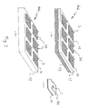
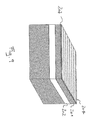
- 1 generally represents a mold according to a first embodiment of the invention.
- the mold 1 essentially comprises a first layer 2 made of a first preset material whose upper surface has, in relief, a first plurality of structures or projections 3 (first projections), which according to the invention have a free end portion with a substantially pointed profile having a curvature radius comprised between 5 nm and 100 nm, preferably comprised between 5 nm and 20 nm.
- the mold 1 allows obtaining, on a substrate, an array of nanotubes parallel to each other arranged vertically with a high control of their positioning, and purposely, according to the invention, the abovementioned projections 3 form actual points or rods having a shape which can be schematically represented as a cone.
- the height of the first projections 3 is comprised between 100 nm and 10 microns, preferably between 300 nm and 1 micron.
- the mold according to the invention whose method of realisation and the relative use shall be outlined in detail in the description hereinafter, can be advantageously made of various material provided the abovementioned projections are conductive and connected electrically.
- the abovementioned first projections 3 of the mold 1, and thus the first layer on which they are obtained can be made of material such as silicon, a metal, a metal alloy, or of a polymer made conductive by coating, therefore the mold 1 can be of the so-called "rigid” type, or of the so-called “soft” type.
- a second plurality of projections 4 can be provided on the upper surface of the first layer 2.
- such second projections 4 are provided with a height exceeding the one of the first projections 3, the height difference being comprised between 10 nm and 100 nm, preferably between 15 nm and 30 nm.
- the second projections 4 form spacers which, in the use of the mold help the maintenance of a preset limited distance between a substrate (not shown in the abovementioned figures) and the first projections 3, as better observed hereinafter.
- the abovementioned second projections 4 may not require an end portion with a particularly pointed profile and their ends can have a width, for example, comprised between 10 and 200 nm.
- the second projections 4, contrary to the first projections 3, may not even require being conductive and, in fact, according to a further characteristic of the invention, they may be insulating.
- the second projections 4 can have a shape schematically represented as a cylinder, frustoconical or parallelepiped-shaped and they are arranged on the first layer 2 preferably alternating to the first projections 3, as illustrated in the example of figure 2 showing second substantially cylindrical-shaped projections.
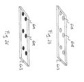
- each second projection can also be provided in the form of a ring 4a, or any other form also capable of surrounding a relative first projection 3, as shown in the example c) of figure 3 .
- the mold according to the invention for obtaining, on a substrate, an array of nanotubes arranged vertically also comprises a second layer arranged beneath and coupled to the abovementioned first layer.
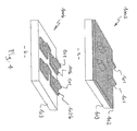
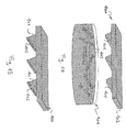
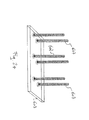
- a mold 10a, 10b comprising a first discontinuous layer 11 of a first preset material on which the abovementioned first projections 3 are provided, and a second layer 12 of a second preset material coupled to the first layer 11 on a surface opposite the one having the projections 3.
- the first layer 11 preferably comprises doped silicon, while the second layer 12 is advantageously a polymer layer.
- the present mold is defined as of the “combined” type, that is “rigid/ soft”.
- the abovementioned second polymer layer 12 serves to confer the mold 10a, 10b, in particular the rigid portion of the mold when it is being used to obtain an array of carbon nanotubes, with the capacity to react elastically to possible non-uniformities at contact between the projections 3 and a substrate.
- the second layer can comprise a large variety of polymer materials given that polymers can have an elastic behaviour, especially when it comes to small deformations.
- thermosetting polymers with elastomeric properties having a high deformation capacity under stress, and a high capacity to recover from the deformation upon the end of the stress, are preferred.
- Polymers of this type comprise polymer chains linked to each other by means of chemical bonds, which allow recovering from an externally induced deformation.
- polymers examples include NBR (butadiene-Acrylonitrile, EP (ethylene-propylene) and SBR (styrene-butadiene).
- the thickness of the second polymer layer 12 it should be added that it is determined by the function that the second layer itself may have, which might be limited to conferring to the present mold the abovementioned elastic properties (mold 10a, figure 3-a ), or additionally, an actual function of supporting the first layer on which the projections 3 are arranged (mold 10b, figure 3-b ).
- the second polymer layer 12 forms an actual support for the first layer 11
- its thickness is generally greater than 10 microns, preferably comprised between 50 microns and 1 mm.
- the present mold advantageously also comprises a third layer 13 arranged beneath the second layer 12.
- the first layer it should be noted that it can be a continuous layer, for example a doped silicon layer of small thickness, or the first layer 11 can be a discontinuous layer, right as shown in the example of figure 3-a) - 3-b) , in which each projection 3 is located on a respective portion of the first layer or pad 3a.
- the abovementioned pads 3a are electrically connected to each other and they are at a distance in comprised between 500 nm and 1 mm, preferably comprised between 1 micron and 100 microns.
- the mold 10a, 10b can comprise a metal film between the first layer 11 and the second layer 12, or a metal mask reproducing the pattern of the mold can be arranged on the upper surface of the mold, the abovementioned electrical connections not being represented in the abovementioned figures.
- the mold 10a, 10b that is, the rigid/soft type of mold can comprise a second plurality of insulating projections (second projections) and whose height is greater than the first projections 3, analogously to the description outlined previously for the mold 1 and as shown in the detail of the example of figure 3-c) .
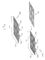
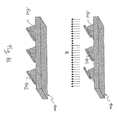
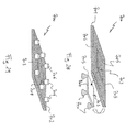
- the present embodiment provides a mold 100a, 100b, schematically illustrated in the example of figure 4-a) - 4-b) comprising a first layer on which the first projections 101 are characterised in that they also have a preset length comprised between 10 nm and 10 microns, preferably between 10 nm to 100 nm.
- the mold 100a, 100b comprises first projections 101 having an end portion with a substantially pointed profile, which can be schematically represented in the form of a polyhedron with a trapezoidal cross-section, whose smaller base (free end) has a width substantially smaller than the width of the greater base, comprised between 5 nm and 100 nm and preferably comprised between 5 nm and 20 nm, that is, comparable with the one of the first projections 3 realised in the form of rods, and a length as considered above.
- the mold considered in this case is similar to the examples of the molds described above regarding the possibility to be of the rigid type, or of the soft type, or of the combined rigid/soft type, with or without the third layer, and with the first layer being continuous or forming pads; therefore regarding such characteristics, see the description above, here below being only briefly described the non-limiting example of figure 4 , wherein:
- the abovementioned first projections 101 can be suitably functionalised whenever desired.
- the abovementioned first projections 101 of the mold 100a, 100b depending on the case can or cannot be conductive and connected electrically, given that such mold can be used to attain an array of horizontally arranged nanotubes according to an alternative embodiment of the method according to the invention, as better observed hereinafter.
- the present mold in particular in the so-called rigid and rigid/soft molds embodiments described above, is obtained according to the invention through a method comprising the steps of:
- the present mold can have conductive and electrically connected or non-connected first projections, substantially shaped as rods or also provided with a given length.
- a first approach to obtain the electrical conduction characteristic includes using a substrate whose abovementioned upper surface is conductive and continuous as previously described.
- the abovementioned substrate is of the rigid type, for example silicon, it can be coupled to a polymer layer to realise a mold of the rigid/ soft type.
- a rigid/soft mold with a first rigid and continuous layer may provide for a relative small thickness of the first layer in such a manner to have the abovementioned characteristics of flexibility and elasticity as argued beforehand.
- the present method preferably further comprises the steps of:
- the present method further comprises the alternative steps of:
- the removal of the abovementioned lower oxide layer 202 is obtained through selective acid etching, for example using HF solutions while, advantageously, the abovementioned preset polymer layer 103, metal coated or not, can be supported on a third layer, preferably a further silicon layer.
- the abovementioned projections of the first plurality of projections have a same height comprised between 100 nm and 10 microns, preferably comprised between 300 nm and 1 micron, and they have a pointed end portion of the same width or the same curvature radius comprised between 5 nm and 100 nm, preferably comprised between 5 and to 20 nm, depending on the geometry of the abovementioned pattern provided on the resist layer.
- the resist layer in the abovementioned figures indicated with 204, is developed in a conventional manner to obtain the abovementioned pattern comprising, in case of a mold for obtaining an array of horizontally arranged nanotubes, a plurality of substantially rectangular windows 205 ( figure 6a ), or comprising in the case of a mold for obtaining an array of vertically arranged nanotubes, a plurality of spots or dots, depending on the type of first projections desired to be realised in the mold.
- thermal oxide layer indicated with 207 obtained through the abovementioned windows are respective rectangular oxide masks 205a, in case of a mold for obtaining an array comprising horizontally arranged nanotubes ( figure 7-a ), or oxide masks substantially forming spots or dots, in case of a mold for obtaining an array comprising vertical nanotubes, indicated with 206a in the example of figure 10-a .
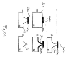
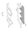
- the abovementioned plurality of first projections having substantially sloping side walls 300 is obtained on the upper silicon layer (first layer).
- FIG 8a-b an upper silicon layer 201 on the upper side of which is obtained the abovementioned mask 206a in the form of an oxide spot or dot.
- figure 8a-c is represented a first projection with substantially sloping side walls 300 as obtained following the abovementioned selective wet etching exploiting the mask 206a.
- first rod-shaped projections 3 shall be defined or, alternatively as argued previously, a plurality of substantially extended first projections.
- the relative pointed end portion has a length comprised between 10 nm and 10 microns, preferably comprised between 10 nm and 100 nm.
- the present mold may also comprise a second plurality of projections 4 (second projections or spacers) taller with respect to the first projections 3.
- the present method comprises providing on the abovementioned resist layer 204 a preset pattern comprising various geometries, that is, the first plurality of spots or dots described above for obtaining the first projections 3 and a second plurality of bigger spots or dots for obtaining the second projections 4.
- oxide masks 206a as described previously and bigger oxide masks 206c, as shown in the example of figure 10-a ).
- the height difference between the second and the first projections which according to the present invention is comprised between 10 nm and 100 nm, preferably comprised between 15 nm and 30 nm.
- the width of the second projections 4, at their end portions, is preferably comprised between 10 nm and 200 nm.
- the abovementioned second projections 4 are electrically insulating contrary to the first projections which, when in the rod-shaped form, as the case now being considered, may be electrically conductive.
- the method according to the invention provides for some alternatives.
- the abovementioned upper silicon layer 201 is a doped silicon layer on which first and second conductive projections 3, 4a are initially obtained.
- the second conductive projections 4a are then made selectively insulating (indicated with 4 in f igure 11-b )) through an oxygen implantation step followed by thermal treatment.
- a selective oxidation of the second conductive projections 4a can be performed by means of an implantation mask which substantially covers the entire substrate 200 and leaves the second projections exposed to a high concentration of oxygen.
- the abovementioned upper silicon layer can be a non-doped layer on which first and second non-conductive projections are initially obtained.
- the upper silicon layer is then made conductive alongside the first projections through a doping step performed by means of ion implantation.
- an upper initially non-doped silicon layer 201c was selectively doped and made conductive alongside first initially non-doped projections 3c, while the second projections 4 not subjected to the doping step remain substantially non-conductive.
- the doping agent can advantageously be any element capable of making the silicon conductive.
- a doping method with a phosphorous concentration comprised between 10 14 and 10 20 atoms/cm 3 , preferably comprised between 10 18 and 10 20 atoms/cm 3 and a subsequent thermal treatment performed in order to make uniform the doping agent in the silicon layer can be used.
- the thermal treatment is performed at a temperature comprised between 300°C and 1100°C, preferably comprised between 700°C and 1100°C.
- the upper silicon later 201 has a thickness comprised between 1 and 100 microns, preferably comprised between 1 and 5 microns, while the lower oxide layer 202, which as described above is substantially a sacrificial layer no longer present in the mold, has a thickness comprised between 0.2 and 1.5 microns, preferably comprised between 0.5 and 1 micron.
- the abovementioned third layer preferably made of silicon, mentioned beforehand referring to the description of the present mold and indicated with 13, can be deemed substantially irrelevant to the object of the present method and may serve as a support in the same method of production of the present mold, whose thickness is comprised between 300 and 725 microns.
- such third layer 13 can be used as an actual support layer in the mold, for example for supporting the polymer layer 103, in which case its thickness is preferably comprised between 500 and 700 microns.
- a mold comprising an upper continuous silicon layer (first initially non-doped layer), having a small thickness such to be flexible, on which the following are arranged: first conductive projections in form of rod-shaped elements and second non-conductive projections 4 in form of spacers, a second polymer layer 103 coupled with the upper layer on a face opposite to the one bearing the abovementioned projections and a third layer 13 coupled with the underside of the second polymer layer 103.
- the method of realisation of the mold illustrated in the example of figure 12-a is particularly advantageous in case of use of a SOI wafer as argued above, such SOI wafer allowing micromachining on an already thin layer (upper layer or first layer) and which is supported in such micromachining step, thus its thinning to obtain the first projections and possibly the second projections is particularly controllable and easy as well as inexpensive.
- the present mold in the various embodiments described above is advantageously used to obtain an array of carbon nanotubes with a high control of their position.
- the present mold is used in some of its embodiments in a method for obtaining an array of horizontally arranged nanotubes, and in other embodiments in a method for obtaining an array of vertically arranged carbon nanotubes.
- the carbon nanotubes 402 are deposited by means of contact molding, as illustrated in the example of figure 17 .
- the abovementioned mold 400, and in particular the first projections of the mold are not required to have particular conductive properties and they can also be insulating, as mentioned beforehand.
- the first projections of the present mold have an end portion with substantially pointed profile at which the high curvature generates high surface energy useful for the adhesion of functionalized carbon nanotubes.
- the substrate on which the array is obtained is made of oxidisable material.
- 501 is used to indicate the abovementioned substrate which comprises an upper surface made of such oxidisable material, advantageously silicon.
- the carbon nanotubes 402 are deposited through a growing step on the substrate 501, then on the carbon nanotubes 402 themselves, of an oxide layer.
- the oxide layer practically fixes the carbon nanotubes mechanically on the substrate 501, as shown in the example of figure 18 , wherein carbon nanotubes 403 can be observed covered by the oxide layer.
- the mold comprises first projections 101a conductive and electrically connected to each other, and the oxide layer is grown through local oxidation applying a voltage impulse between such first conductive projections 101a and the substrate 501 in a highly wet environment.
- the first projections serve as a cathode and the water meniscus provides the electrolyte for producing the oxidation of the substrate surface.
- the oxidation of the substrate generates the abovementioned oxide layer which encloses and locks the carbon nanotubes on the substrate itself.
- each first projection of the mold is occupied by a respective nanotube perfectly aligned to it.
- the present method involves, following the step of wetting the first projections in the dispersion, the further step of removing any carbon nanotubes not entirely adherent to a respective first projection by subjecting the mold to an electric field (E), and thus repeating the step of wetting the first projections of the mold in the dispersion, as illustrated in the example of figure 16 in which carbon nanotubes 402 not entirely adherent to respective first projections are shown along with the application of an electric field for their removal.
- E electric field
- the nanotubes used are functionalized, for example with surfactants or DNA molecules, or also through covalent functionalizations.
- the surfactants among which sodium dodecyl sulfate (SDS) is included are preferred.
- the abovementioned method as mentioned above regarding the layers of the mold, can be performed using rigid, soft and also the combined rigid/soft type of molds as described previously.
- the main advantage of the method described above lies in the fact, that due to the use of the present mold, the realised array comprises carbon nanotubes arranged horizontally in a highly controlled manner due to a highly assisted parallel deposition.
- an array comprising carbon nanotubes the deposition of which, at particularly accurate positions, can be advantageously performed both in organic and inorganic substrates is obtained.
- the present array can be advantageously obtained at particularly low process temperatures.
- the present invention provides a method, schematically illustrated in the example of figures 19-24 , advantageously used in which is a mold of the type described previously which for simplification purposes is shown in a manner limited to a first layer only comprising first conductive projections, the method comprising:
- the CVD ( chemical vapour deposition) technique is a PECVD (plasma enhanced CVD) technique performed with plasma.
- PECVD plasma enhanced CVD
- the oxide layer formed on the catalytic nanoparticles it should be added that it is preferably obtained by means of an anisotropic etching, for example by means of plasma.
- the aim is to free a limited portion of each catalytic nanoparticle from the oxide layer, in such a manner that it can serve as a catalytic crystallization nucleus, but simultaneously leaving the catalytic nanoparticle substantially, mechanically, fixed to the substrate through the oxide layer itself.
- the present method involves the repetition of the abovementioned steps of forming the water meniscus and oxidation of the relative catalytic nanoparticles n number of times, substantially horizontally moving each time of such n times the relative position between the mold and the substrate, that is, the abovementioned preset spaced relation is realised with relative different horizontal positions between the mold and the surface covered by catalytic nanoparticles.
- the abovementioned upper surface of the partially oxidized substrate is a surface functionalised and locally oxidized through a relative local oxidation step in which a plurality of oxide spots 608 according to the pattern of the mold 600 ( figure 25 ) is realised on the upper surface of the substrate.
- the method according to the invention further comprises, before the step of depositing the abovementioned layer of catalytic nanoparticles 604 on the substrate 603, the further step of:
- the abovementioned cavities 609 form energetically favoured positions for the deposition of catalytic nanoparticles 604 ( figure 27 ) and they shall be substantially occupied by a respective catalytic nanoparticle.
- the abovementioned locally oxidised surface portion of the substrate is obtained by applying a voltage impulse between the projections of the mold and the same surface portion in a highly wet environment, analogously to the points argued previously.
- the present method may comprise, before the deposition of the layer of catalytic nanopoarticles, the further steps of locally growing a native oxide layer in the abovementioned cavities 609.
- the localisation and arrangement of the particles in the cavities is additionally favored.
- such a functionalization if on one side it prevents the formation of native oxide on the substrate, on the other it can be locally removed at the abovementioned cavities following the local oxidation induced by the electric field in a wet environment.
- the substrate surface portion outside the cavities is thus still functionalised with the -NH 2 terminations, while inside the cavities there is a native oxide layer, which favours the subsequent deposition of the catalytic nanoparticles inside the same cavities.
- the catalytic nanoparticles have a diameter comprised between 1 nn and 200 nm, even more preferably comprised between 1 nm and 50 nm.
- the abovementioned deposition of catalytic nanoparticles is performed starting from a dispersion of nanoparticles in a preset solvent, or alternatively by using a synthetic DNA lattice.
- an inhibitor layer advantageously oleic acid, covers the catalytic nanoparticles.
- the catalytic nanoparticles are initially deposited on the substrate in such a manner that they do not aggregate with each other and somehow adhere to the substrate itself, depending on the adhesion force involved which depends on the different chemical properties of the material forming the substrate and the catalytic nanoparticles.
- the selective removal of the particles not fixed through the oxide onto the substrate can be obtained by intervening on the abovementioned adhesion force, for example through the use of a liquid (solvent) in a washing step through which the substrate/nanorparticle adhesion is lowered.
- a liquid solvent
- the abovementioned method for obtaining an array of vertically arranged carbon nanotubes can be realised by means of rigid, soft and also the combined rigid/soft types of molds, possibly also comprising a second plurality of the spacer type of projections taller than the first projections, as described previously.
- the main advantage of the method described above lies in the possibility of first obtaining a preset catalytic pattern, comprising catalytic sites (catalytic nanoparticles) with highly controlled positions and dimensions, at a particularly low cost given that expensive techniques such as advanced lithography processes are not used.
- the present method allows obtaining, through a parallel execution, an array of carbon nanotubes parallel to each other and arranged vertically, with high control of their positioning and also of their dimensions, in particular of the radius, which basically depends on the dimensions of the catalytic sites obtained on the substrate.
- the catalytic sites are not influenced by limits given by the lithography processes given that they depend on the initial dimensions of the catalytic nanoparticles which can be initially of dimensions reduced to a few nanometres.
- An effective control on the positioning on a substrate of a plurality of nanotubes is substantially required in electronic applications using carbon nanotubes, such as for example in transistors and in the probe memories.
- the present method allows obtaining carbon nanotubes through a parallel approach, having a high control of their positioning, and also having a high control of the dimension and of the uniformity of the nanotubes.
- arrays of nanotubes obtained according to the invention have interesting applications in many electronic products, for example as field emitters (display, manufacturing low cost photomasks, compact microwave amplifiers, gas sensors), in probe memories, in the photonic technology industry, in transistors, biosensors etc.
- the present method for obtaining an array of vertically arranged carbon nanotubes can be realised by means of a mold illustrated schematically in the example of figure 28 .
- a mold indicated in its entirety with 700 comprises a first layer 701 with an upper surface 702 having a first projection 703 having a side wall 704 substantially perpendicular to such upper surface 702, which identifies a plurality of corners 705.
- the mold 700 comprises one first substantially square-shaped projection 703, therefore four corners 705, but it is understood that the present mold may comprise a greater number of first projections even of a different shape and therefore with a greater number of corners.
- the mold 700 may also comprise a plurality of second projections 706 taller than the first projection 703, i.e. projections of the spacer type considered previously with reference to the different embodiments of the mold already described according to the invention.
- the first projection 703 may not have an end portion with a substantially pointed profile, therefore the mold, and in particular the abovementioned first layer of the mold, can be advantageously made starting from templates obtained with less intense processes that comprise, moreover, fewer realisation steps.
- a soft mold made of polymer material, is manufactured through simple replica on a rigid template having a complementary structure which can be used for a high number of times.
- the second projections are insulating while the first projection is electrically conductive and therefore makes also the abovementioned corners conductive and electrically connected.
- the electric conductivity can be obtained by metallizing the upper surface of the first layer thus the first projection and not metallizing the abovementioned spacers.
- Such metallization can be obtained by means of a thin metal film or by means of an appropriate metal mask arranged on the upper surface of the mold.
- a first soft layer can possibly be supported on the lower part by a second layer not shown in the figures.
- the mold 700 is used according to the invention in a method for obtaining, on a substrate, an array of carbon nanotubes parallel to each other and arranged vertically.
- Such method during the performance of its steps, is similar to the method described above for obtaining an array of vertically arranged carbon nanotubes except for the fact of using a different mold.
- the growth of nanotubes at highly localised positions occurs by exploiting the abovementioned corners 705 of the first projection 703, given that at such corners, analogously to points illustrated previously and as shown in the detail of figure 28 the formation of a water meniscus 710 can be obtained, therefore the oxidation of the catalytic nanoparticles, their locking on the substrate and the relative growth of nanotubes with a high control of their positioning.
Landscapes
- Engineering & Computer Science (AREA)
- Chemical & Material Sciences (AREA)
- Nanotechnology (AREA)
- Physics & Mathematics (AREA)
- Manufacturing & Machinery (AREA)
- Crystallography & Structural Chemistry (AREA)
- General Physics & Mathematics (AREA)
- Condensed Matter Physics & Semiconductors (AREA)
- Mathematical Physics (AREA)
- Theoretical Computer Science (AREA)
- Microelectronics & Electronic Packaging (AREA)
- Carbon And Carbon Compounds (AREA)
- Cold Cathode And The Manufacture (AREA)
- Analysing Materials By The Use Of Radiation (AREA)
- Moulds For Moulding Plastics Or The Like (AREA)
Abstract
Description
- The present invention, in its most general aspect, refers to the electronics sector, and in particular to nanoelectronics and nanomanufacturing.
- More in particular, the invention refers to molds having nanometric features, to their realisation and corresponding use in methods for realising arrays of carbon nanotubes.
- Carbon nanotubes are the object of a considerable and constantly growing interest in the nanoelectronics sector, which still today is not yet capable of fully exploiting its exceptional features and properties, in particular in field emission devices.
- Single wall carbon nanotubes and multiple wall nanotubes show an excellent electrical conductivity at room temperature.
- Carbon nanotubes are different from the metal emitters in that, in the latter, the electrical resistance increases with increasing temperature, the heat increasing proportionally with the increase in the extracted current. This causes an unstable heat dispersion, which inevitably leads to the destruction of the emission source in the metal type emitters. On the other hand, however, nanotubes are very stable emitters even at very high temperatures, due to the fact that their electrical resistance decreases with temperature, thus limiting the generated heat.
- In addition, other features such as the exceptionally reduced size, the ballistic conduction, the high transport mobility, and the absence of electronic migration make the carbon nanotubes ideal candidates for transistor type applications and for the interconnections in electronic devices.
- Even though recently, realisation and use techniques have been developed for carbon nanotubes of a certain interest, these new materials are still far from being industrially utilised, mainly due to the difficulties encountered in managing them, which may make their positioning control particularly problematic. In order to properly exploit carbon nanotube features, it is helpful to effectively control their relative position on a substrate.
- The prior art, for example, provides a horizontal positioning method of nanotubes based on the nanomanipulation, which includes using an AFM rod for moving single nanotubes onto a substrate.
- Other gripping devices have been made that are capable of ensuring a precise control of the horizontal positioning of nanotubes, which nevertheless allow the grip from one site and the release in a final position of a single nanotube at a time.
- It is understood that techniques of this type may be limited to the realisation of prototypes of devices comprising horizontally-arranged nanotube arrays, since they are serial techniques which may not easily be applied on an industrial scale.
- Other techniques provided in the prior art, such as ink jet printing, dielectrophoresis, and stamp printing, permit the deposition in parallel of nanotubes on a substrate, and at competitive costs.
- For example, by means of the ink jet technique, a dispersion of nanotubes can be printed following preset patterns, or it can be deposited between two electrodes, with orientation and fixing of nanotubes, by means of dielectrophoresis. Moreover, nanotubes deposited on a first substrate can be taken by means of a mold of the so-called soft type and deposited by means of contact printing on a second substrate according to the pattern in relief on the mold.
- The main drawback of such techniques lies in the fact that they are solely applicable for the realisation of nanotube networks.
- Furthermore, the known art provides for processes in which the nanotubes are not arranged and/or handled on a substrate but directly grown, that is realised, on them.
- In the process of horizontal growth of nanotubes, a silicon substrate is engraved creating grooves or trenches in which the growth of nanotubes occurs between an edge and another of the grooves or trenches. However, such processes may not guarantee a well-controlled final position of the nanotubes.
- On the contrary, by engraving a catalyst layer deposited on the substrate, also in this case realising grooves or trenches, in which nanotubes are formed, better results are attained in terms of controlling the position of the nanotubes on the substrate. However, such better results may be diminished by the fact that the diameter of a nanotube depends of the width of the groove in which it grows, which in turn depends on the resolution of the patterning technique used to create the groove. The obtainment of particularly small diameters, thus nanotubes with a high potential, necessarily implies the use of extremely costly lithography techniques which, furthermore, do not guarantee a nanotube diameter smaller than a given limit (about 20 nm).
- Also in order to obtain an array of nanotubes arranged vertically on a substrate, the prior art provides processes in which the nanotubes are grown directly on the substrate.
- In particular, nanotubes are grown on a substrate through a technique known as CVD (chemical vapour deposition). The growth process occurs by means of aggregation of carbon atoms, supplied by a high temperature hydrocarbon gas in a nanotube crystalline structure generated by a nanometric size metal particle which serves as a catalyser and crystallisation nucleus. For example, methane gas at 900°C and at a pressure of 750 torr can be used as a source of carbon.
- Though there are several procedures for obtaining catalyst nanoparticles (distributed on a substrate) on which carbon nanotubes can be grown, an effective control of the position of each nanotube is currently attained by using e-beam lithography techniques which allow localising, on the substrate, spots or dots at desired positions.
- In such a manner, it is possible to obtain vertically oriented parallel nanotubes having highly controlled positions, but the entire realisation procedure may be particularly slow and very costly due to the use of the e-beam lithography and, therefore, may not be acceptable in a large scale industrialisation like the one used currently for electronic production.
- Additionally, there still remains however a limit to the smallest dimension of the abovementioned catalyst spots which can be obtained through e-beam lithography.
- Therefore, the need to realise (on a substrate) an array of nanotubes of particularly small dimensions with a high control of their positioning, both in case of horizontal orientation and in case of vertical orientation, at a cost allowing its industrialisation in the manufacture of electronic devices, has yet to be met.
- The present invention provides means for realising, on a preset substrate, an array of carbon nanotubes with a high control of their position.
- The term "to realise an array" means that an array comprising a preset number of carbon nanotubes is directly obtained as such, that is through a parallel approach in which the preset number of nanotubes is directly and globally obtained on the substrate, thus not using a serial repetition for each single nanotube.
- The term "array of nanotubes" means a plurality of nanotubes arranged on a substrate at controlled positions, and having a horizontal orientation, or having a vertical orientation.
- Therefore, according to a first aspect, the invention provides a mold, and a related method of realisation, for directly obtaining, on a substrate, an array of carbon nanotubes, in which said mold has a preset pattern in relief coinciding with the pattern of the array of nanotubes to be obtained.
- According to a second aspect, the present invention provides a method in which said mold is used for realising an array of carbon nanotubes.
- According to the invention, attained are arrays of carbon nanotubes in which the nanotubes are in highly controlled positions on a substrate, defined by the pattern of the mold used, both in case of an array with horizontally arranged nanotubes, and in case of an array with vertically arranged nanotubes, as better observed hereinafter.
- In particular, the invention relates to a method for realising a mold for obtaining an array of carbon nanotubes comprising the steps of:
- a) providing a substrate of a preset material having an upper surface;
- b) thermally growing, on said upper surface, a first layer of thermal oxide;
- c) depositing, on said first layer of thermal oxide, a layer of photosensitive material;
- d) realising, on said layer of photosensitive material, a preset pattern through lithography patterning;
- e) developing said layer of photosensitive material and etching said first thermal oxide layer obtaining a thermal oxide mask with geometry corresponding to said preset pattern;
- f) selectively etching said upper surface of said substrate obtaining on it beneath said mask a first plurality of projections having substantially sloping side walls;
- g) filing said first plurality of projections having substantially sloping side walls by means of plasma etching;
- h) thermally growing, on said upper surface of said substrate, a second oxide layer thus further filing said first plurality of projections having substantially sloping side walls;
- i) selectively removing said second thermal oxide layer and said mask thus freeing said upper surface of said substrate obtaining a first plurality of projections thereon having an end with a substantially pointed profile.
- According to one aspect of the invention, said substrate is a SOI wafer comprising an upper silicon layer and a lower oxide layer, wherein said upper surface is an upper surface of said upper silicon layer and comprising the further steps of:
- l) selectively etching said lower oxide layer with its removal;
- m) coupling, by means of a photosensitive glue layer, said upper silicon layer comprising said first plurality of projections having an end with a substantially pointed profile to a layer of a preset polymer;
- According to this aspect of the invention, the method further comprising the steps of:
- q) making said upper silicon layer discontinuous by realizing a plurality of pads each comprising a respective projection of said first plurality of projections, said pads being separated by a distance comprised between 500 nm and 1 mm, preferably comprised between 1 micron and 100 microns.
- o) electrically connecting said pads to each other through a metal mask having a geometry corresponding to said preset pattern.
- According to another aspect of the invention, said substrate is a SOI wafer comprising an upper silicon layer and a lower oxide layer, wherein said upper surface is an upper surface of said upper silicon layer, comprising the further steps of:
- l) selectively etching said lower oxide layer with its removal;
- p) coupling, by means of a photosensitive glue layer, said upper silicon layer comprising said first plurality of projections having an end with a substantially pointed profile to a metallized surface of a layer of a preset polymer;
- q) making said upper silicon layer discontinuous by realizing a plurality of pads each comprising a respective projection of said first plurality of projections, said pads being separated by a distance comprised between 500 nm and 1 mm, preferably comprised between 1 micron and 100 microns.
- In particular, said layer of a preset polymer is supported by a third layer, preferably a silicon layer.
- According to another aspect of the invention said projections of said first plurality of projections substantially have the same height comprised between 100 nm and 10 microns.
- According to this aspect of the invention, said height is comprised between 300 nm and 1 micron.
- According to yet another aspect of the invention, said projections of said first plurality of projections have a pointed end portion substantially of the same width or have the same curvature radius comprised between 5 nm and 100 nm.
- According to this aspect of the invention, said width or said curvature radius is comprised between 5 nm and 20 nm.
- According to another aspect of the invention, said end portion of said first plurality of projections has a length comprised between 10 nm and 10 microns.
- According to this aspect of the invention, 11. Method according to claim 10, wherein said length is comprised between 10 nm and 100 nm.
- According to another aspect of the invention, said preset pattern comprises two different types of designs and through said steps f) - h) a second plurality of projections is realised being taller than said projections of said first plurality of projections.
- According to this aspect of the invention, the height difference between the projections of said second plurality and the projections of said first plurality is comprised between 10 nm and 100 nm.
- Moreover, wherein said height difference is comprised between 15 nm and 30 nm.
- According to another aspect of the invention, said projections of said second plurality of projections have an end portion substantially of the same width comprised between 10 nm and 200 nm.
- According to yet another aspect of the invention, at least some projections of said first plurality of projections are surrounded by respective projections of said second plurality of projections.
- According to another aspect of the invention, said projections of said first plurality of projections are electrically conductive and said projections of said second plurality of projections are electrically insulating.
- In particular, said first silicon layer is a doped layer and said projections of said second plurality of projections are made selectively insulating through an oxygen implantation step followed by a thermal treatment.
- Moreover, said first silicon layer is a non-doped layer made selectively conductive together with said projections of said first plurality of projections through an ion implantation step.
- The invention also relates to a mold for obtaining an array of carbon nanotubes characterised in that it comprises a first layer of a first preset material having a surface having in relief at least one first plurality of projections having a free end portion with a substantially pointed profile, said end having a width or a curvature radius comprised between 5 nm and 100 nm.
- According to one aspect of the invention, said width or said curvature radius is comprised between 5 nm and 20 nm.
- According to another aspect of the invention, said first material is a metal, a metal alloy, a polymer or silicon.
- According to yet another aspect of the invention, the mold further comprises a second layer of a second preset material coupled with said first layer on a surface opposite to said surface presenting said projections.
- In particular, said first layer is a discontinuous layer comprising a plurality of pads, each pad comprising a respective projection of said first plurality of projections.
- According to another aspect of the invention, said projections of said first plurality of projections are electrically connected.
- According to yet another aspect of the invention, said projections of said first plurality substantially have the same height comprised between 100 nm and 10 microns.
- According to this aspect of the invention, said height is comprised between 300 nm and 1 micron.
- According to another aspect of the invention, said free end of said projections of said first plurality has a length comprised between 10 nm and 10 microns.
- According to this aspect of the invention, wherein said length is comprised between 10 nm and 100 nm.
- According to another aspect of the invention, the mold further comprises a second plurality of projections having a free end portion, wherein said projections of said second plurality are taller than said projections of said first plurality.
- According to another aspect of the invention, the height difference between the projections of said second plurality and the projections of said first plurality is comprised between 10 nm and 100 nm.
- According to this aspect of the invention, said height difference is comprised between 15 nm and 30 nm.
- According to another aspect of the invention, said projections of said second plurality of projections have a free end portion substantially of the same width comprised between 10 nm and 200 nm.
- According to yet another aspect of the invention, at least one projection of said first plurality is substantially surrounded by a projection of said second plurality.
- According to a further aspect of the invention, said projections of said first plurality of projections are electrically conductive and said projections of said second plurality of projections are electrically insulating.
- In particular, said first material is silicon and said second material is a polymer.
- The invention also relates to the use of a mold as previously described for realising an array of carbon nanotubes on a substrate.
- Moreover, the invention further relates to a method for realising an array of horizontally arranged carbon nanotubes comprising the steps of:
- providing a mold comprising a first layer of a first preset material having a surface having in relief at least one plurality of projections arranged according to a preset pattern, said projections having a free end portion with a substantially pointed profile, said end having a length comprised between 10 nm and 10 microns and a width comprised between 5 nm and 100 nm.
- providing a dispersion of functionalized carbon nanotubes having dimensions comparable to said projections;
- wetting said projections of said first plurality of projections in said dispersion in such a manner that to said projections adhere respective carbon nanotubes;
- depositing, in an assisted manner through said mold, said carbon nanotubes on said substrate obtaining said horizontally arranged carbon nanotubes.
- According to one aspect of the invention, said carbon nanotubes are deposited by means of contact molding.
- According to another aspect of the invention, said substrate has an upper surface made of an oxidisable material.
- In particular, said oxidisable material is silicon.
- According to another aspect of the invention, wherein said carbon nanotubes are deposited by means of local oxidation, said method comprising the further step of growing on said substrate and on said nanotubes an oxide layer thus mechanically fixing said nanotubes on said substrate.
- According to another aspect of the invention, said projections of said first plurality of projections are conductive and said oxide layer is obtained by applying a voltage impulse between said projections and said substrate in a highly wet environment
- According to yet another aspect of the invention, the method further comprises, subsequently to the step of wetting said projections of said first plurality of projections in said dispersion, a step of removing possible carbon nanotubes not entirely adherent to the respective projections by subjecting said mold to an electric field and repeating the step of wetting said projections in said dispersion.
- According to this aspect of the invention, said step of removing and repeating said step of wetting said projections are repeated until each one of said projections is coupled with a respective nanotube substantially entirely aligned therewith.
- According to another aspect of the invention, said nanotubes are functionalized using surfactants, DNA molecules or by means of covalent functionalizations.
- In particular, said surfactant is sodium dodecyl sulfate (SDS).
- According to another aspect of the invention, said substrate is functionalized.
- In particular, said projections are functionalized.
- The invention further relates to a method for realising an array of vertically arranged carbon nanotubes comprising the steps of:
- providing a mold comprising a first layer of a first preset material having a surface having in relief at least one first plurality of projections arranged according to a preset pattern said projections being conductive and having a free end portion with a substantially pointed profile, said end having a curvature radius comprised between 5 nm and 100 nm;
- providing a substrate having an upper surface oxidisable or partially oxidised with a native oxide film;
- depositing, on said substrate, a uniform layer of catalytic nanoparticles essentially having the same radius substantially entirely covering at least a preset portion of said surface of said substrate;
- arranging, in a highly wet environment, said mold in a preset spaced relation with said surface portion covered by said layer of catalytic nanoparticles, up to the formation of a water meniscus between each projection and an underlying respective nanoparticle;
- applying a voltage impulse between said projections and said surface portion generating at each meniscus an oxide layer on each respective nanoparticle thus fixing it on said substrate;
- selectively removing the portion of nanoparticles not fixed on said surface portion of said substrate, obtaining a catalytic nanoparticle pattern corresponding to the pattern of said mold;
- subjecting said nanopaticles fixed on said substrate to a controlled etching thus partially removing from each nanoparticle said oxide layer with relative partial exposure of each particle;
- growing carbon nanotubes from said catalytic nanoparticles of said nanoparticles pattern, through the CVD technique, obtaining said array of vertically arranged carbon nanotubes.
- According to one aspect of the invention, said CVD technique is performed by means of plasma through PECVD.
- Moreover, according to another aspect of the invention, said steps of forming water meniscus and oxidation of the respective nanoparticles are repeated for a preset n number of times, for each of said n times said preset spaced relation being realised with different relative positions between said mold and said surface portion covered by nanoparticles.
- According to yet another aspect of the invention, said substrate is functionalized in such a manner that chemical species having an -NH2 termination are bonded to said at least one surface portion.
- According to another aspect of the invention, said upper surface of the substrate is functionalized, the method further comprising, before the step of depositing said nanoparticles on said substrate, the further steps of:
- locally oxidising said portion of said surface realising a plurality of oxide spots according to the pattern of said mold;
- selectively etching and removing said oxide spots obtaining a relative pattern of cavities cut in said surface portion of said substrate; and
before or after depositing said layer of catalytic nanoparticles, the step of - aligning said pattern of said mold to said pattern of said cavities.
- According to this aspect of the invention, the method further comprising the step of locally growing an oxide layer in said cavities.
- According to another aspect of the invention, the local oxidation of said surface portion is obtained by applying a voltage impulse between said projections of said mold and said surface portion of said substrate in a highly wet environment.
- According to yet another aspect of the invention, said catalytic nanoparticles have a diameter comprised between 1 nn and 200 nm.
- Moreover, said diameter is comprised between 1 nm and 50 nm.
- According to yet another aspect of the invention, the deposition of said nanoparticles is performed starting from a dispersion of said nanoparticles in a preset solvent.
- According to another aspect of the invention, said catalytic nanoparticles are covered by a passivating layer.
- According to this aspect of the invention, said passivating layer is oleic acid.
- According to yet another aspect of the invention, the deposition of said particles is performed through a synthetic DNA lattice.
- Furthermore, the invention relates to a mold for obtaining an array of vertically arranged carbon nanotubes characterised in that it comprises a first polymer layer having a surface having at least one first projection with a preset geometry, said at least one first projection being conductive and having a side wall substantially perpendicular to such surface having a plurality of corners.
- According to another aspect of the invention, said surface of said first polymer layer is metallized at least at said first projection.
- According to yet another aspect of the invention, the mold further comprises a plurality of second insulating projections taller than said at least one first projection.
- According to a further aspect of the invention, the mold further comprises a second layer coupled with said first polymer layer on one of its surfaces opposite the surface having said at least one first projection.
- Finally, the invention relates to the use of a mold as previously described in a method for obtaining an array of vertically arranged carbon nanotubes.
- Further characteristics and advantages of the present invention shall be clear from the description, provided hereinafter, of some of its embodiments provided for indicative and non-limiting purposes with reference to the attached figures.
- In such figures:
-
Figures 1-3 schematically show a mold for obtaining, on a substrate, an array of vertically arranged carbon nanotubes according to some embodiments of the present invention; -
Figures 4 and5 schematically show a mold for obtaining, on a substrate, an array of carbon nanotubes arranged horizontally according to other embodiments of the invention; -
Figures 6-8 schematically show some steps of a method according to the invention for realizing some embodiments of the molds offigures 4 and5 ; -
Figures 8a-13 schematically show some steps of a method according to the invention for realizing some embodiments of the molds offigures 1-3 ; -
Figures 14-17 schematically show some steps of a method according to the invention for obtaining, on a substrate, an array of horizontally arranged nanotubes; -
Figure 18 schematically shows another embodiment of the method illustrated infigures 14-17 ; -
Figures 19-24 schematically show some steps of a method according to the invention for obtaining, on a substrate, an array of vertically arranged carbon nanotubes; -
Figures 25-27 schematically show another embodiment of the method illustrated infigures 19-24 ; -
Figures 28 and 29 schematically show a mold for obtaining, on a substrate, an array of vertically arranged carbon nanotubes according to other embodiments of the present invention; - It should be observed that the abovementioned figures are not in scale but made in such a manner to highlight the characteristics of the invention which advantageously allow the obtainment, on a substrate, of an array of carbon nanotubes in highly controlled positions, with the nanotubes themselves arranged horizontally or vertically, as better observed hereinafter.
- In detail, referring to
figure 1, 1 generally represents a mold according to a first embodiment of the invention. - The
mold 1 essentially comprises afirst layer 2 made of a first preset material whose upper surface has, in relief, a first plurality of structures or projections 3 (first projections), which according to the invention have a free end portion with a substantially pointed profile having a curvature radius comprised between 5 nm and 100 nm, preferably comprised between 5 nm and 20 nm. - The
mold 1 allows obtaining, on a substrate, an array of nanotubes parallel to each other arranged vertically with a high control of their positioning, and purposely, according to the invention, theabovementioned projections 3 form actual points or rods having a shape which can be schematically represented as a cone. - The height of the
first projections 3 is comprised between 100 nm and 10 microns, preferably between 300 nm and 1 micron. - The mold according to the invention, whose method of realisation and the relative use shall be outlined in detail in the description hereinafter, can be advantageously made of various material provided the abovementioned projections are conductive and connected electrically.
- In particular, the abovementioned
first projections 3 of themold 1, and thus the first layer on which they are obtained, can be made of material such as silicon, a metal, a metal alloy, or of a polymer made conductive by coating, therefore themold 1 can be of the so-called "rigid" type, or of the so-called "soft" type. - According to an embodiment of the present mold illustrated in the example of
figure 2 , a second plurality of projections 4 (second projections) can be provided on the upper surface of thefirst layer 2. - In this case, such
second projections 4 are provided with a height exceeding the one of thefirst projections 3, the height difference being comprised between 10 nm and 100 nm, preferably between 15 nm and 30 nm. - The
second projections 4 form spacers which, in the use of the mold help the maintenance of a preset limited distance between a substrate (not shown in the abovementioned figures) and thefirst projections 3, as better observed hereinafter. - Therefore, contrary to the
first projections 3, the abovementionedsecond projections 4 may not require an end portion with a particularly pointed profile and their ends can have a width, for example, comprised between 10 and 200 nm. - The
second projections 4, contrary to thefirst projections 3, may not even require being conductive and, in fact, according to a further characteristic of the invention, they may be insulating. - The
second projections 4 can have a shape schematically represented as a cylinder, frustoconical or parallelepiped-shaped and they are arranged on thefirst layer 2 preferably alternating to thefirst projections 3, as illustrated in the example offigure 2 showing second substantially cylindrical-shaped projections. - According to the invention each second projection can also be provided in the form of a ring 4a, or any other form also capable of surrounding a relative
first projection 3, as shown in the example c) offigure 3 . - According to an alternative and particularly advantageous embodiment, the mold according to the invention for obtaining, on a substrate, an array of nanotubes arranged vertically also comprises a second layer arranged beneath and coupled to the abovementioned first layer.
- In particular, schematically represented in
figure 3 is a mold 10a, 10b comprising a firstdiscontinuous layer 11 of a first preset material on which the abovementionedfirst projections 3 are provided, and asecond layer 12 of a second preset material coupled to thefirst layer 11 on a surface opposite the one having theprojections 3. - In such case, the
first layer 11 preferably comprises doped silicon, while thesecond layer 12 is advantageously a polymer layer. - The present mold is defined as of the "combined" type, that is "rigid/ soft".
- The abovementioned
second polymer layer 12 serves to confer the mold 10a, 10b, in particular the rigid portion of the mold when it is being used to obtain an array of carbon nanotubes, with the capacity to react elastically to possible non-uniformities at contact between theprojections 3 and a substrate. - Advantageously, the second layer can comprise a large variety of polymer materials given that polymers can have an elastic behaviour, especially when it comes to small deformations.
- The thermosetting polymers with elastomeric properties having a high deformation capacity under stress, and a high capacity to recover from the deformation upon the end of the stress, are preferred.
- Polymers of this type comprise polymer chains linked to each other by means of chemical bonds, which allow recovering from an externally induced deformation.
- Examples of such polymers are NBR (butadiene-Acrylonitrile, EP (ethylene-propylene) and SBR (styrene-butadiene).
- Regarding the thickness of the
second polymer layer 12, it should be added that it is determined by the function that the second layer itself may have, which might be limited to conferring to the present mold the abovementioned elastic properties (mold 10a,figure 3-a ), or additionally, an actual function of supporting the first layer on which theprojections 3 are arranged (mold 10b,figure 3-b ). - In case the
second polymer layer 12 forms an actual support for thefirst layer 11, its thickness is generally greater than 10 microns, preferably comprised between 50 microns and 1 mm. - In case the
second polymer layer 12 does not form an actual support for thefirst layer 11, the present mold advantageously also comprises athird layer 13 arranged beneath thesecond layer 12. - The presence of the
third layer 13 of substantially rigid material that serves as a support for the second layer and in practice for the entire mold, allows reducing the dimensions of thesecond layer 12 to a thickness greater than 30 nm, preferably comprised between 100 nm and 10 microns. - Regarding the first layer it should be noted that it can be a continuous layer, for example a doped silicon layer of small thickness, or the
first layer 11 can be a discontinuous layer, right as shown in the example offigure 3-a) - 3-b) , in which eachprojection 3 is located on a respective portion of the first layer or pad 3a. - In case of a first
discontinuous layer 11 the abovementioned pads 3a are electrically connected to each other and they are at a distance in comprised between 500 nm and 1 mm, preferably comprised between 1 micron and 100 microns. - The electrical connection of the pads 3a can be realised in various ways, for example, the mold 10a, 10b can comprise a metal film between the
first layer 11 and thesecond layer 12, or a metal mask reproducing the pattern of the mold can be arranged on the upper surface of the mold, the abovementioned electrical connections not being represented in the abovementioned figures. - It should be added, according to the invention, that the mold 10a, 10b, that is, the rigid/soft type of mold can comprise a second plurality of insulating projections (second projections) and whose height is greater than the
first projections 3, analogously to the description outlined previously for themold 1 and as shown in the detail of the example offigure 3-c) . - In order to obtain, on a substrate, an array of horizontally arranged carbon nanotubes, with a high control of their positioning, the present embodiment provides a
mold 100a, 100b, schematically illustrated in the example offigure 4-a) - 4-b) comprising a first layer on which thefirst projections 101 are characterised in that they also have a preset length comprised between 10 nm and 10 microns, preferably between 10 nm to 100 nm. - In particular, the
mold 100a, 100b, comprisesfirst projections 101 having an end portion with a substantially pointed profile, which can be schematically represented in the form of a polyhedron with a trapezoidal cross-section, whose smaller base (free end) has a width substantially smaller than the width of the greater base, comprised between 5 nm and 100 nm and preferably comprised between 5 nm and 20 nm, that is, comparable with the one of thefirst projections 3 realised in the form of rods, and a length as considered above. - The mold considered in this case is similar to the examples of the molds described above regarding the possibility to be of the rigid type, or of the soft type, or of the combined rigid/soft type, with or without the third layer, and with the first layer being continuous or forming pads; therefore regarding such characteristics, see the description above, here below being only briefly described the non-limiting example of
figure 4 , wherein: - a) the mold 100a comprises a first
continuous layer 102 realised on which is a plurality offirst projections 101, and asecond polymer layer 103.
It should be advantageously noted that in this case the abovementioned continuousfirst layer 102 is particularly thin, that is, with a limited preset thickness in such a manner that it is also provided with a given flexibility, in such a manner that the entire mold 100a has the capacity, also due to the underlyingsecond polymer layer 103, to react elastically against possible contact non-uniformities, as argued beforehand. - b) the
mold 100b comprises a first discontinuous layer, that is, it has a plurality of pads 102b each of which has a respectivefirst projection 101, and asecond layer 103 positioned at the lower side and coupled to the first layer in form of pads. - In any case, in the
mold 100a, 100b according to the invention, independent of the type, that is, regardless of whether dealing with a rigid, soft or rigid/soft mold like the one shown infigure 4 , the abovementionedfirst projections 101 can be suitably functionalised whenever desired.. - Furthermore, according to the invention and contrary to the example of the mold described above with reference to an array of vertical nanotubes, the abovementioned
first projections 101 of themold 100a, 100b depending on the case can or cannot be conductive and connected electrically, given that such mold can be used to attain an array of horizontally arranged nanotubes according to an alternative embodiment of the method according to the invention, as better observed hereinafter. - Therefore, also regarding the abovementioned characteristic of the electrical conduction see the preceding description, only briefly describing in the following for non-limiting purposes through the examples of
figure 5 : - a) a mold 100c comprising a plurality of
first projections 101 arranged on a first discontinuous layer in form of pads 102b, and asecond polymer layer 103 having a metal coated surface 103a on which the pads 102b are arranged; - b) a
mold 100d comprising a plurality offirst projections 101 arranged on a first discontinuous layer in form of pads 102b, asecond polymer layer 103 arranged below and coupled to the first layer, and ametal mask 104 having a geometric pattern reproducing the one of the upper surface of the mold. - The present mold, in particular in the so-called rigid and rigid/soft molds embodiments described above, is obtained according to the invention through a method comprising the steps of:
- a) providing a substrate of a preset material having an upper surface;
- b) thermally growing, on such upper surface, a first layer of thermal oxide;
- c) depositing, on the first layer of thermal oxide, a layer of photosensitive material, for example resist;
- d) realizing, on the layer of photosensitive resist, a preset pattern through optical lithography or e-beam lithography patterning;
- e) developing the resist layer and etching the first thermal oxide layer obtaining a thermal oxide mask with geometry corresponding to the abovementioned preset pattern;
- f) selectively etching the upper surface of the substrate obtaining on it, beneath the abovementioned mask, a first plurality of projections having substantially sloping side walls;
- g) filing the plurality of projections having substantially sloping side walls by means of plasma etching;
- h) thermally growing, on the upper surface of the substrate, a second oxide layer thus further filing the first plurality of projections having substantially sloping side walls;
- i) selectively removing the second thermal oxide layer and the abovementioned mask freeing the upper surface of the substrate, obtaining a first plurality of projections thereon having an end with a substantially pointed profile.
- As argued above the present mold can have conductive and electrically connected or non-connected first projections, substantially shaped as rods or also provided with a given length.
- A first approach to obtain the electrical conduction characteristic includes using a substrate whose abovementioned upper surface is conductive and continuous as previously described.
- Furthermore, if the abovementioned substrate is of the rigid type, for example silicon, it can be coupled to a polymer layer to realise a mold of the rigid/ soft type.
- It should be noted that a rigid/soft mold with a first rigid and continuous layer may provide for a relative small thickness of the first layer in such a manner to have the abovementioned characteristics of flexibility and elasticity as argued beforehand.
- By using, as a substrate, a SOI (silicon on insulator) wafer indicated in its entirety with 200, the abovementioned method of realisation of a mold comprising
first projections 101 for realizing an array of horizontally arranged nanotubes is schematically illustrated in a preferred embodiment in the examples offigures 6-8a , while infigures 9-13 the method is schematically illustrated in the case the realisation of a mold comprisingfirst projections 3 for realizing an array of vertically aligned nanotubes is desired, as argued beforehand. - In detail, starting from the abovementioned SOI wafer comprising an
upper silicon layer 201 and alower oxide layer 202, wherein the abovementioned upper surface of the substrate corresponds to an upper surface 201a of theupper silicon layer 201, the present method preferably further comprises the steps of: - l) selectively etching the
lower oxide layer 202 with its removal; - m) coupling, by a photosensitive glue layer, the
upper silicon layer 201 comprising the first plurality of projections 101 (or comprising first projections 3) having an end with a substantially pointed profile to a layer of apreset polymer 103; - n) optionally making the
upper silicon layer 201 discontinuous realizing respective pads 102b (or realizing respective pads 3a) each comprising a respective projection, wherein such pads are separated by a distance comprised between 500 nm and 1 mm, preferably comprised between 1 micron and 100 microns; - o) electrically connecting the abovementioned pads 102b to each other (or electrically connecting the pads 3a to each other) then the projections of the first plurality of projections through a
metal mask 104 having a geometry corresponding to the abovementioned preset pattern, like the one shown infigure 13-b) relatively to a mold havingfirst projections 3 in form of rods, or also as shown in the previous example offigure 5-b) regarding a mold havingfirst projections 101 for obtaining horizontally arranged carbon nanotubes. - Or, still considering a SOI wafer of the abovementioned type, the present method further comprises the alternative steps of:
- l) selectively etching the
lower oxide layer 202 with its removal; - p) coupling, through a photosensitive glue layer, the
upper silicon layer 201 comprising the first plurality of projections 101 (or comprising the first plurality of projections 3) having an end with a substantially pointed profile to a metal coated surface 103a of apreset polymer layer 103, as illustrated in the previous example offigure 5-a) ; - q) making the
upper silicon layer 201 discontinuous realizing a plurality of pads 102b (or realizing a plurality of pads 3a) each comprising a respective projection of the first plurality of projections, wherein the pads are separated from each other by a distance comprised between 500 nm and 1 mm, preferably comprised between 1 micron and 100 microns (figure 8 ,figure 13-a) ). - In any case, preferably, the removal of the abovementioned
lower oxide layer 202 is obtained through selective acid etching, for example using HF solutions while, advantageously, the abovementionedpreset polymer layer 103, metal coated or not, can be supported on a third layer, preferably a further silicon layer. - According to the present method, the abovementioned projections of the first plurality of projections (first projections) have a same height comprised between 100 nm and 10 microns, preferably comprised between 300 nm and 1 micron, and they have a pointed end portion of the same width or the same curvature radius comprised between 5 nm and 100 nm, preferably comprised between 5 and to 20 nm, depending on the geometry of the abovementioned pattern provided on the resist layer.
- With regard to this, it should be added that the resist layer, in the abovementioned figures indicated with 204, is developed in a conventional manner to obtain the abovementioned pattern comprising, in case of a mold for obtaining an array of horizontally arranged nanotubes, a plurality of substantially rectangular windows 205 (
figure 6a ), or comprising in the case of a mold for obtaining an array of vertically arranged nanotubes, a plurality of spots or dots, depending on the type of first projections desired to be realised in the mold. - Still in a conventional manner, then by etching the abovementioned thermal oxide layer indicated with 207, obtained through the abovementioned windows are respective rectangular oxide masks 205a, in case of a mold for obtaining an array comprising horizontally arranged nanotubes (
figure 7-a ), or oxide masks substantially forming spots or dots, in case of a mold for obtaining an array comprising vertical nanotubes, indicated with 206a in the example offigure 10-a . - Through a selective wet etching, by exploiting the abovementioned masks, the abovementioned plurality of first projections having substantially sloping side walls 300 (
figure 7-b ), is obtained on the upper silicon layer (first layer). - This latter step, along with the steps of progressive filing of the first projections forming the relative end portions with a substantially pointed profile, is schematically illustrated, with regard to a single first rod-shaped
projection 3, in the example offigure 8a . - It should be observed that the example indicated in
figure 8a and described hereinafter is valid even in casefirst projections 101 of a given length are desired. - In particular, in
figure 8a-b ) is shown anupper silicon layer 201 on the upper side of which is obtained the abovementioned mask 206a in the form of an oxide spot or dot. - In
figure 8a-c ) is represented a first projection with substantially slopingside walls 300 as obtained following the abovementioned selective wet etching exploiting the mask 206a. - Subsequently, as aforementioned, follows a plasma etching, for example an SF6 etching (
figure 8a-d )) obtained through which is a first filing of the first projection. - Then follows a thermal oxide growing step with the formation on the
upper silicon layer 201 of a second oxide layer indicated with 301 which occurs on the, and at the expense of the, upper surface 201 a of thefirst layer 201, in particular at the expense of the first projection, having the substantially sloping side walls, already filed previously for the first time. In this step (figure 8a-e )) a further filing of the first projection is carried out thus forming a relative end portion with substantially pointed profile, which is still covered by thesecond oxide layer 301. - The subsequent removal of the mask 206a and of the
second oxide layer 301 frees the upper surface of the substrate (first layer) thus defined on which shall be the abovementioned first rod-shaped projection 3 (figure 8a-f )). - Obviously, in practice, a plurality of first rod-shaped
projections 3 shall be defined or, alternatively as argued previously, a plurality of substantially extended first projections. - In case of substantially extended
first projections 101, the relative pointed end portion has a length comprised between 10 nm and 10 microns, preferably comprised between 10 nm and 100 nm. - According to the invention, as previously described, in particular in case of first rod-shaped projections, the present mold may also comprise a second plurality of projections 4 (second projections or spacers) taller with respect to the
first projections 3. - In order to obtain such second projections the present method comprises providing on the abovementioned resist layer 204 a preset pattern comprising various geometries, that is, the first plurality of spots or dots described above for obtaining the
first projections 3 and a second plurality of bigger spots or dots for obtaining thesecond projections 4. - Then obtained from such geometries of the pattern are the respective oxide masks, that is, oxide masks 206a as described previously and bigger oxide masks 206c, as shown in the example of
figure 10-a ). - By optimising the surface area difference between the abovementioned masks 206a and 206c (that is the sizes of the spots when patterning the resist layer 204), it is possible to vary the height difference between the second and the first projections which according to the present invention is comprised between 10 nm and 100 nm, preferably comprised between 15 nm and 30 nm.
- The width of the
second projections 4, at their end portions, is preferably comprised between 10 nm and 200 nm. - Obviously, as described beforehand, it is possible to obtain variously shaped spacers through a suitable patterning of the resist layer, for example it is even possible to obtain a ring-shaped spacer; in this case a first projection shall be substantially surrounded by a relative spacer.
- According to the invention, and as previously argued, the abovementioned
second projections 4 are electrically insulating contrary to the first projections which, when in the rod-shaped form, as the case now being considered, may be electrically conductive. - In order to differentiate, from the electrical conduction point of view, the first projections from the second projections, the method according to the invention provides for some alternatives.
- In an embodiment illustrated in the example of
figure 10-b ), the abovementionedupper silicon layer 201 is a doped silicon layer on which first and secondconductive projections 3, 4a are initially obtained. The second conductive projections 4a are then made selectively insulating (indicated with 4 in figure 11-b )) through an oxygen implantation step followed by thermal treatment. - In this case, a selective oxidation of the second conductive projections 4a can be performed by means of an implantation mask which substantially covers the
entire substrate 200 and leaves the second projections exposed to a high concentration of oxygen. - Following the implantation which preferably leads to a concentration of oxygen in the second projections comprised between 1016 and 1018, a thermal treatment at a temperature comprised between 750°C and 959°C, in a nitrogen atmosphere, generates the desired insulating oxide from oxygen thus forming the abovementioned second
insulating projections 4. - According to another embodiment, the abovementioned upper silicon layer, on the contrary, can be a non-doped layer on which first and second non-conductive projections are initially obtained. The upper silicon layer is then made conductive alongside the first projections through a doping step performed by means of ion implantation.
- In this case, shown in the example of
figure 11-a ), an upper initially non-doped silicon layer 201c was selectively doped and made conductive alongside first initiallynon-doped projections 3c, while thesecond projections 4 not subjected to the doping step remain substantially non-conductive. - The doping agent can advantageously be any element capable of making the silicon conductive.
- For example, a doping method with a phosphorous concentration comprised between 1014 and 1020 atoms/cm3, preferably comprised between 1018 and 1020 atoms/cm3 and a subsequent thermal treatment performed in order to make uniform the doping agent in the silicon layer can be used. The thermal treatment is performed at a temperature comprised between 300°C and 1100°C, preferably comprised between 700°C and 1100°C.
- Still, regarding the upper silicon layer and in particular the entire SOI wafer, some further considerations should be added.
- In detail, the upper silicon later 201 has a thickness comprised between 1 and 100 microns, preferably comprised between 1 and 5 microns, while the
lower oxide layer 202, which as described above is substantially a sacrificial layer no longer present in the mold, has a thickness comprised between 0.2 and 1.5 microns, preferably comprised between 0.5 and 1 micron. - The abovementioned third layer, preferably made of silicon, mentioned beforehand referring to the description of the present mold and indicated with 13, can be deemed substantially irrelevant to the object of the present method and may serve as a support in the same method of production of the present mold, whose thickness is comprised between 300 and 725 microns.
- Alternatively, such
third layer 13 can be used as an actual support layer in the mold, for example for supporting thepolymer layer 103, in which case its thickness is preferably comprised between 500 and 700 microns. - With regard to this, in the example of
figure 12-a ) a mold is shown 310 comprising an upper continuous silicon layer (first initially non-doped layer), having a small thickness such to be flexible, on which the following are arranged: first conductive projections in form of rod-shaped elements and secondnon-conductive projections 4 in form of spacers, asecond polymer layer 103 coupled with the upper layer on a face opposite to the one bearing the abovementioned projections and athird layer 13 coupled with the underside of thesecond polymer layer 103. - It should be observed that the method of realisation of the mold illustrated in the example of
figure 12-a ) is particularly advantageous in case of use of a SOI wafer as argued above, such SOI wafer allowing micromachining on an already thin layer (upper layer or first layer) and which is supported in such micromachining step, thus its thinning to obtain the first projections and possibly the second projections is particularly controllable and easy as well as inexpensive. - The points argued above also apply to the alternative embodiments of the present mold, just like the ones shown in particular in the example of
figure 12-b ) in which a mold 310a analogous to the mold offigure 12-a ) but without the third layer is shown, and in the example offigure 13-a ) in which a mold 310b analogous to the one offigure 12-b ) however in which the first layer is discontinuous is shown, that is, obtained in the form of pads 3a as described previously. - According to the invention the present mold, in the various embodiments described above is advantageously used to obtain an array of carbon nanotubes with a high control of their position.
- In particular, the present mold is used in some of its embodiments in a method for obtaining an array of horizontally arranged nanotubes, and in other embodiments in a method for obtaining an array of vertically arranged carbon nanotubes.
- In the examples of
figures 14-18 schematically illustrated is the first of the abovementioned two methods wherein for simplification purposes amold 400 is shown in a manner limited to the layer comprising the first projections being well understood that actually it could also comprise the second and possibly the third layer as described previously, the method essentially comprising the steps of: - providing a
mold 400 of the type considered above, comprising afirst layer 102 of a first preset material having a surface having in relief at least a plurality offirst projections 101 arranged according to a preset pattern having a free end portion with substantially pointed profile, wherein such first projections have a length comprised between 10 nm and 10 microns and a width comprised between 5 nm and 100 nm. - providing a
dispersion 401 offunctionalized carbon nanotubes 402 having dimensions comparable to the dimensions of the abovementionedfirst projections 101; - wetting the abovementioned
first projections 101 in thedispersion 401, that is bringing such first projections into contact with such dispersion, in such a manner that tofirst projections 101 adhererespective carbon nanotubes 402; - assisted deposition, through the
abovementioned mold 400, of thecarbon nanotubes 402 on asubstrate 500 thus obtaining the abovementioned array of horizontally arranged carbon nanotubes. - According to an embodiment of the present invention the
carbon nanotubes 402 are deposited by means of contact molding, as illustrated in the example offigure 17 . - In such case, the
abovementioned mold 400, and in particular the first projections of the mold are not required to have particular conductive properties and they can also be insulating, as mentioned beforehand. - It should be observed that the adhesion between the mold and the nanotubes occur spontaneously in a manner depending on the structure or the pattern of the mold, that is, depending on the first projections.
- The first projections of the present mold, as described previously, have an end portion with substantially pointed profile at which the high curvature generates high surface energy useful for the adhesion of functionalized carbon nanotubes.
- According to an alternative embodiment of the present invention, illustrated in the example of
figure 18 regarding the final step of the abovementioned method, the substrate on which the array is obtained is made of oxidisable material. - In particular, in
figure 18 , 501 is used to indicate the abovementioned substrate which comprises an upper surface made of such oxidisable material, advantageously silicon. - In such embodiment of the present method, the
carbon nanotubes 402 are deposited through a growing step on thesubstrate 501, then on thecarbon nanotubes 402 themselves, of an oxide layer. - The oxide layer practically fixes the carbon nanotubes mechanically on the
substrate 501, as shown in the example offigure 18 , whereincarbon nanotubes 403 can be observed covered by the oxide layer. - In particular, in such case, the mold comprises first projections 101a conductive and electrically connected to each other, and the oxide layer is grown through local oxidation applying a voltage impulse between such first conductive projections 101a and the
substrate 501 in a highly wet environment. - In a highly wet environment the application of a voltage impulse between the first conductive projections and a substrate positioned at a limited preset distance from the first projections, or even also at contact with the nanotubes attached on them, polarises the water molecules in vapour phase and the ones adsorbed on the surface of the substrate.
- When the voltage impulse reaches and exceeds a given threshold value a water meniscus is formed between the first projections and the substrate, induced by the generated electric field.
- In this case, the first projections serve as a cathode and the water meniscus provides the electrolyte for producing the oxidation of the substrate surface.
- The oxidation of the substrate generates the abovementioned oxide layer which encloses and locks the carbon nanotubes on the substrate itself.
- It should be observed that such embodiment of the present invention is particularly advantageous in case of applications of the transistor type, in which nanotubes substantially covered by an oxide layer, just like the ones obtained in the example of
figure 18 are required. - In a preferred embodiment of the present invention it is possible to operate in such a manner that each first projection of the mold is occupied by a respective nanotube perfectly aligned to it.
- In fact, to prevent a nanotube from occupying, so to say, only a portion of the relative first projection, thus remaining hanging therefrom, the present method involves, following the step of wetting the first projections in the dispersion, the further step of removing any carbon nanotubes not entirely adherent to a respective first projection by subjecting the mold to an electric field (E), and thus repeating the step of wetting the first projections of the mold in the dispersion, as illustrated in the example of
figure 16 in whichcarbon nanotubes 402 not entirely adherent to respective first projections are shown along with the application of an electric field for their removal. - The abovementioned last two steps of removal by means of an electric field and wetting can be repeated n times until each projection is coupled with a respective nanotube substantially entirely and perfectly aligned with it.
- What occurs in this case is that the adhesion force between a nanotube not perfectly aligned with a relative first projection and the projection itself is lower than the adhesion force in case of a perfectly aligned nanotube, i.e. when the contact interface is maximum.
- Such difference of forces is exploited to remove possible poorly arranged nanotubes through the abovementioned uniform electric field which is substantially applied vertically with respect to the mold.
- By modulating the intensity of the electric field it is possible to remove possible nanotubes even differently but still poorly arranged on the projections which have a lower adhesion to the mold.
- By repeating such procedure, intermitted by relative dipping (wetting) of the first projections of the mold into the dispersion of nanotubes, it is possible to obtain that each projection be occupied by a nanotube exploiting the entire front surface available for the projection itself.
- In any case, in the embodiments described above, in order to optimise the realisation of a stable dispersion the nanotubes used are functionalized, for example with surfactants or DNA molecules, or also through covalent functionalizations.
- The surfactants among which sodium dodecyl sulfate (SDS) is included are preferred.
- Furthermore it is also possible to provide for a functionalization of the substrate and of the first projections of the mold, to be selected depending on the functionalization of the carbon nanotubes.
- The abovementioned method, as mentioned above regarding the layers of the mold, can be performed using rigid, soft and also the combined rigid/soft type of molds as described previously.
- The main advantage of the method described above lies in the fact, that due to the use of the present mold, the realised array comprises carbon nanotubes arranged horizontally in a highly controlled manner due to a highly assisted parallel deposition.
- Therefore, through a low cost method, an array comprising carbon nanotubes the deposition of which, at particularly accurate positions, can be advantageously performed both in organic and inorganic substrates is obtained.
- Furthermore, given that direct growth of nanotubes from the substrates is not required, the present array can be advantageously obtained at particularly low process temperatures.
- It should be observed that in the examples indicated above the horizontally arranged carbon nanotubes are shown aligned and parallel to each other according to the mold used; however, according to the invention, when required it is possible to use a mold with a pattern in which the first projections are realised in such a manner to obtain an array of carbon nanotubes arranged horizontally but not parallel to each other.
- In order to obtain, on a substrate, an array of carbon nanotubes parallel to each other and arranged vertically, the present invention provides a method, schematically illustrated in the example of
figures 19-24 , advantageously used in which is a mold of the type described previously which for simplification purposes is shown in a manner limited to a first layer only comprising first conductive projections, the method comprising: - providing a
mold 600 comprising afirst layer 601 of a first preset material having a surface having in relief at least a first plurality ofprojections 602 arranged according to a preset pattern, in which suchfirst projections 602 are conductive, electrically connected to each other, and have a free end portion with substantially pointed profile having a curvature radius comprised between 5 nm and 100 nm; - providing a
substrate 603 having an oxidisable or partially oxidised upper surface with a native oxide film; - depositing on the substrate 603 a uniform layer of
catalytic nanoparticles 604 essentially having the same radius substantially entirely covering at least a preset portion of such substrate surface 603 (figure 19 ); - arranging the
mold 600, in a highly wet environment, at a preset spaced relation with the substrate surface portion covered by thecatalytic nanoparticles layer 604 up to the formation between eachfirst projection 602 and an underlyingrespective nanoparticle 604 of awater meniscus 605, analogously to the points already described (figure 20 ); - applying a voltage impulse between the abovementioned
first projections 602 and the abovementioned substrate surface portion, generating at eachwater meniscus 605 anoxide layer 606 on each relativecatalytic nanoparticle 604 with its fixation on the substrate 603 (figure 21 ); - selectively removing the
catalytic nanoparticle portion 604 not fixed on the abovementioned substrate surface portion, thus obtaining a pattern ofcatalytic nanoparticles 604 corresponding to the pattern of thefirst projections 602 of the mold 600 (figure 22 ); - subjecting the
catalytic nanoparticles 604 fixed onto thesubstrate 603 to a controlled etching partially removing from each nanoparticle theoxide layer 606 with the relative partial exposure of each particle (figure 23 ): - growing from the
catalytic nanoparticles 604 from the abovementioned pattern of nanoparticles therespective carbon nanotubes 607 by means of the CVD technique, obtaining the abovementioned array of vertically arranged carbon nanotubes 607 (figure 24 ). - Preferably, the CVD (chemical vapour deposition) technique is a PECVD (plasma enhanced CVD) technique performed with plasma.
- With regard to the selective and partial removal of the oxide layer formed on the catalytic nanoparticles, it should be added that it is preferably obtained by means of an anisotropic etching, for example by means of plasma.
- In practice, the aim is to free a limited portion of each catalytic nanoparticle from the oxide layer, in such a manner that it can serve as a catalytic crystallization nucleus, but simultaneously leaving the catalytic nanoparticle substantially, mechanically, fixed to the substrate through the oxide layer itself.
- A gas mixture which allows a non-aggressive etching, of the oxide layer, for example F2/Ar, is therefore preferred.
- Advantageously, according to the invention, it is possible to obtain an array with a density of carbon nanotubes even greater than the density of the first projections present on the mold.
- In this case, the present method involves the repetition of the abovementioned steps of forming the water meniscus and oxidation of the relative catalytic nanoparticles n number of times, substantially horizontally moving each time of such n times the relative position between the mold and the substrate, that is, the abovementioned preset spaced relation is realised with relative different horizontal positions between the mold and the surface covered by catalytic nanoparticles.
- According to a schematised embodiment in the example of
figures 25-27 , the abovementioned upper surface of the partially oxidized substrate is a surface functionalised and locally oxidized through a relative local oxidation step in which a plurality ofoxide spots 608 according to the pattern of the mold 600 (figure 25 ) is realised on the upper surface of the substrate. The method according to the invention further comprises, before the step of depositing the abovementioned layer ofcatalytic nanoparticles 604 on thesubstrate 603, the further step of: - selectively etching and removing the
abovementioned oxide spots 608 obtaining a relative pattern ofcavities 609 cut in the abovementioned upper portion of the substrate 603 (figure 26 ); - aligning the pattern of the
mold 600 to the pattern of thecavity 609 of thesubstrate 603. - In this case, the
abovementioned cavities 609 form energetically favoured positions for the deposition of catalytic nanoparticles 604 (figure 27 ) and they shall be substantially occupied by a respective catalytic nanoparticle. - Preferably, the abovementioned locally oxidised surface portion of the substrate, that is its local oxidation, is obtained by applying a voltage impulse between the projections of the mold and the same surface portion in a highly wet environment, analogously to the points argued previously.
- Still, the present method may comprise, before the deposition of the layer of catalytic nanopoarticles, the further steps of locally growing a native oxide layer in the
abovementioned cavities 609. - In this case, the localisation and arrangement of the particles in the cavities is additionally favored.
- Advantageously the points described above made particularly effective due to the above-mentioned functionalization of the substrate which is advantageously realised in such a manner that chemical species having an -NH2 termination are bonded to the abovementioned upper surface portion of the substrate.
- In fact, such a functionalization, if on one side it prevents the formation of native oxide on the substrate, on the other it can be locally removed at the abovementioned cavities following the local oxidation induced by the electric field in a wet environment.
- In practice, what occurs is the removal of the functionalization terminating with the -NH2 groups in a manner limited to the oxide spots obtained through the voltage impulse, then there is the removal of the same oxide spots formed with relative realisation of the abovementioned cavities, and then the formation of the native oxide layer locally and limited to the cavity.
- The substrate surface portion outside the cavities is thus still functionalised with the -NH2 terminations, while inside the cavities there is a native oxide layer, which favours the subsequent deposition of the catalytic nanoparticles inside the same cavities.
- This is highly facilitated by the poor affinity the catalytic nanoparticles have for -NH2 groups and by the high affinity they have, on the contrary, for the oxide.
- Preferably, the catalytic nanoparticles have a diameter comprised between 1 nn and 200 nm, even more preferably comprised between 1 nm and 50 nm.
- Advantageously, the abovementioned deposition of catalytic nanoparticles is performed starting from a dispersion of nanoparticles in a preset solvent, or alternatively by using a synthetic DNA lattice.
- Still preferably, an inhibitor layer, advantageously oleic acid, covers the catalytic nanoparticles.
- It is worth noting that the catalytic nanoparticles are initially deposited on the substrate in such a manner that they do not aggregate with each other and somehow adhere to the substrate itself, depending on the adhesion force involved which depends on the different chemical properties of the material forming the substrate and the catalytic nanoparticles.
- The selective removal of the particles not fixed through the oxide onto the substrate, can be obtained by intervening on the abovementioned adhesion force, for example through the use of a liquid (solvent) in a washing step through which the substrate/nanorparticle adhesion is lowered.
- The abovementioned method for obtaining an array of vertically arranged carbon nanotubes, as aforementioned, can be realised by means of rigid, soft and also the combined rigid/soft types of molds, possibly also comprising a second plurality of the spacer type of projections taller than the first projections, as described previously.
- The main advantage of the method described above lies in the possibility of first obtaining a preset catalytic pattern, comprising catalytic sites (catalytic nanoparticles) with highly controlled positions and dimensions, at a particularly low cost given that expensive techniques such as advanced lithography processes are not used.
- Therefore, the present method allows obtaining, through a parallel execution, an array of carbon nanotubes parallel to each other and arranged vertically, with high control of their positioning and also of their dimensions, in particular of the radius, which basically depends on the dimensions of the catalytic sites obtained on the substrate.
- In particular, it should be observed that the catalytic sites are not influenced by limits given by the lithography processes given that they depend on the initial dimensions of the catalytic nanoparticles which can be initially of dimensions reduced to a few nanometres.
- Therefore, advantageously, growth of carbon nanotubes, even with a single wall, is allowed.
- An effective control on the positioning on a substrate of a plurality of nanotubes is substantially required in electronic applications using carbon nanotubes, such as for example in transistors and in the probe memories.
- Furthermore, also the control of the radius of the carbon nanotubes, both in terms of dimension and uniformity in the array is particularly important in most electronic applications widely requested.
- Regarding this, it is useful to emphasise that the present method allows obtaining carbon nanotubes through a parallel approach, having a high control of their positioning, and also having a high control of the dimension and of the uniformity of the nanotubes.
- The combination of the points discussed above is useful for understanding the differences between over what is provided in the prior art.
- As a matter of fact, the prior art, though widely dealing with processes related to the realisation and use of nanotubes, does not meet or does not fully meet the double need linked to the control of the positioning and of the dimensions (uniformity and size) of carbon nanotubes. Therefore, advantageously, arrays of nanotubes obtained according to the invention have interesting applications in many electronic products, for example as field emitters (display, manufacturing low cost photomasks, compact microwave amplifiers, gas sensors), in probe memories, in the photonic technology industry, in transistors, biosensors etc.
- Still, according to an alternative embodiment, the present method for obtaining an array of vertically arranged carbon nanotubes, can be realised by means of a mold illustrated schematically in the example of
figure 28 . - In such figure, a mold indicated in its entirety with 700, comprises a
first layer 701 with anupper surface 702 having afirst projection 703 having aside wall 704 substantially perpendicular to suchupper surface 702, which identifies a plurality ofcorners 705. - In the example of the figure the
mold 700 comprises one first substantially square-shapedprojection 703, therefore fourcorners 705, but it is understood that the present mold may comprise a greater number of first projections even of a different shape and therefore with a greater number of corners. - Furthermore, as shown in the example of
figure 29 , themold 700 may also comprise a plurality ofsecond projections 706 taller than thefirst projection 703, i.e. projections of the spacer type considered previously with reference to the different embodiments of the mold already described according to the invention. - In this case, the
first projection 703 may not have an end portion with a substantially pointed profile, therefore the mold, and in particular the abovementioned first layer of the mold, can be advantageously made starting from templates obtained with less intense processes that comprise, moreover, fewer realisation steps. - More precisely, a soft mold, made of polymer material, is manufactured through simple replica on a rigid template having a complementary structure which can be used for a high number of times.
- Also in this embodiment of the mold according to the invention, analogously to the points argued previously, the second projections (spacers) are insulating while the first projection is electrically conductive and therefore makes also the abovementioned corners conductive and electrically connected.
- The electric conductivity can be obtained by metallizing the upper surface of the first layer thus the first projection and not metallizing the abovementioned spacers.
- Advantageously such metallization can be obtained by means of a thin metal film or by means of an appropriate metal mask arranged on the upper surface of the mold.
- Obviously, a first soft layer can possibly be supported on the lower part by a second layer not shown in the figures.
- In any case, the
mold 700, is used according to the invention in a method for obtaining, on a substrate, an array of carbon nanotubes parallel to each other and arranged vertically. - Such method, during the performance of its steps, is similar to the method described above for obtaining an array of vertically arranged carbon nanotubes except for the fact of using a different mold.
- In this case, the growth of nanotubes at highly localised positions occurs by exploiting the
abovementioned corners 705 of thefirst projection 703, given that at such corners, analogously to points illustrated previously and as shown in the detail offigure 28 the formation of awater meniscus 710 can be obtained, therefore the oxidation of the catalytic nanoparticles, their locking on the substrate and the relative growth of nanotubes with a high control of their positioning. - Therefore, regarding the detailed description of the use of such mold, reference shall be made to the points illustrated previously with reference to a mold comprising first projections substantially in form of rods.
- Obviously, to the embodiments of the invention described above, in order to satisfy specific and contingent needs, a man skilled in the art can make numerous modifications all moreover contained within the scope of protection of the invention, as defined by the following claims.
Claims (34)
- Method for realising a mold for obtaining an array of carbon nanotubes comprising the steps of:a) providing a substrate of a preset material having an upper surface;b) thermally growing, on said upper surface, a first layer of thermal oxide;c) depositing, on said first layer of thermal oxide, a layer of photosensitive material;d) realising, on said layer of photosensitive material, a preset pattern through lithography patterning;e) developing said layer of photosensitive material and etching said first thermal oxide layer obtaining a thermal oxide mask with geometry corresponding to said preset pattern;f) selectively etching said upper surface of said substrate obtaining on it beneath said mask a first plurality of projections having substantially sloping side walls;g) filing said first plurality of projections having substantially sloping side walls by means of plasma etching;h) thermally growing, on said upper surface of said substrate, a second oxide layer thus further filing said first plurality of projections having substantially sloping side walls;i) selectively removing said second thermal oxide layer and said mask thus freeing said upper surface of said substrate obtaining a first plurality of projections thereon having an end with a substantially pointed profile.
- Method according to claim 1, wherein said substrate is a SOI wafer comprising an upper silicon layer and a lower oxide layer, wherein said upper surface is an upper surface of said upper silicon layer and comprising the further steps of:l) selectively etching said lower oxide layer with its removal;m) coupling, by means of a photosensitive glue layer, said upper silicon layer comprising said first plurality of projections having an end with a substantially pointed profile to a layer of a preset polymer;
- Method according to claim 2, further comprising the steps of:q) making said upper silicon layer discontinuous by realizing a plurality of pads each comprising a respective projection of said first plurality of projections, said pads being separated by a distance comprised between 500 nm and 1 mm, preferably comprised between 1 micron and 100 microns.o) electrically connecting said pads to each other through a metal mask having a geometry corresponding to said preset pattern.
- Method according to claim 1, wherein said substrate is a SOI wafer comprising an upper silicon layer and a lower oxide layer, wherein said upper surface is an upper surface of said upper silicon layer, comprising the further steps of:l) selectively etching said lower oxide layer with its removal;p) coupling, by means of a photosensitive glue layer, said upper silicon layer comprising said first plurality of projections having an end with a substantially pointed profile to a metallized surface of a layer of a preset polymer;q) making said upper silicon layer discontinuous by realizing a plurality of pads each comprising a respective projection of said first plurality of projections, said pads being separated by a distance comprised between 500 nm and 1 mm, preferably comprised between 1 micron and 100 microns.
- Method according to claim 2, 3 or 4, wherein said layer of a preset polymer is supported by a third layer, preferably a silicon layer.
- Method according to any one of claims 2-5, wherein said preset pattern comprises two different types of designs and through said steps f) - h) a second plurality of projections is realised being taller than said projections of said first plurality of projections.
- Method according to claim 6, wherein at least some projections of said first plurality of projections are surrounded by respective projections of said second plurality of projections.
- Method according to any one of claims 6-7, wherein said projections of said first plurality of projections are electrically conductive and said projections of said second plurality of projections are electrically insulating.
- Mold for obtaining an array of carbon nanotubes characterised in that it comprises a first layer of a first preset material having a surface having in relief at least one first plurality of projections having a free end portion with a substantially pointed profile, said end having a width or a curvature radius comprised between 5 nm and 100 nm.
- Mold according to claim 9, further comprising a second layer of a second preset material coupled with said first layer on a surface opposite to said surface presenting said projections.
- Mold according to claim 10, wherein said first layer is a discontinuous layer comprising a plurality of pads, each pad comprising a respective projection of said first plurality of projections.
- Mold according to any one of claims 9-11, wherein said projections of said first plurality of projections are electrically connected.
- Mould according to any one of claims 9-12, further comprising a second plurality of projections having a free end portion, wherein said projections of said second plurality are taller than said projections of said first plurality.
- Mold according to claim 13, wherein at least one projection of said first plurality is substantially surrounded by a projection of said second plurality.
- Mold according to any one of claims 13-14, wherein said projections of said first plurality of projections are electrically conductive and said projections of said second plurality of projections are electrically insulating.
- Method for realising an array of horizontally arranged carbon nanotubes comprising the steps of:- providing a mold comprising a first layer of a first preset material having a surface having in relief at least one plurality of projections arranged according to a preset pattern, said projections having a free end portion with a substantially pointed profile, said end having a length comprised between 10 nm and 10 microns and a width comprised between 5 nm and 100 nm.- providing a dispersion of functionalized carbon nanotubes having dimensions comparable to said projections;- wetting said projections of said first plurality of projections in said dispersion in such a manner that to said projections adhere respective carbon nanotubes;- depositing, in an assisted manner through said mold, said carbon nanotubes on said substrate obtaining said horizontally arranged carbon nanotubes.
- Method according to claim 16 wherein said carbon nanotubes are deposited by means of contact molding.
- Method according to claim 16 or 17, wherein said substrate has an upper surface made of an oxidisable material.
- Method according to claim 18, wherein said carbon nanotubes are deposited by means of local oxidation, said method comprising the further step of growing on said substrate and on said nanotubes an oxide layer thus mechanically fixing said nanotubes on said substrate.
- Method according to claim 19, wherein said projections of said first plurality of projections are conductive and said oxide layer is obtained by applying a voltage impulse between said projections and said substrate in a highly wet environment
- Method according to any one of claims 16-20 further comprising, subsequently to the step of wetting said projections of said first plurality of projections in said dispersion, a step of removing possible carbon nanotubes not entirely adherent to the respective projections by subjecting said mold to an electric field and repeating the step of wetting said projections in said dispersion.
- Method according to claim 21, wherein said step of removing and repeating said step of wetting said projections are repeated until each one of said projections is coupled with a respective nanotube substantially entirely aligned therewith.
- Method according to any one of claims 16-22, wherein said nanotubes are functionalized using surfactants, DNA molecules or by means of covalent functionalizations.
- Method for realising an array of vertically arranged carbon nanotubes comprising the steps of:- providing a mold comprising a first layer of a first preset material having a surface having in relief at least one first plurality of projections arranged according to a preset pattern said projections being conductive and having a free end portion with a substantially pointed profile, said end having a curvature radius comprised between 5 nm and 100 nm;- providing a substrate having an upper surface oxidisable or partially oxidised with a native oxide film;- depositing, on said substrate, a uniform layer of catalytic nanoparticles essentially having the same radius substantially entirely covering at least a preset portion of said surface of said substrate;- arranging, in a highly wet environment, said mold in a preset spaced relation with said surface portion covered by said layer of catalytic nanoparticles, up to the formation of a water meniscus between each projection and an underlying respective nanoparticle;- applying a voltage impulse between said projections and said surface portion generating at each meniscus an oxide layer on each respective nanoparticle thus fixing it on said substrate;- selectively removing the portion of nanoparticles not fixed on said surface portion of said substrate, obtaining a catalytic nanoparticle pattern corresponding to the pattern of said mold;- subjecting said nanopaticles fixed on said substrate to a controlled etching thus partially removing from each nanoparticle said oxide layer with relative partial exposure of each particle;- growing carbon nanotubes from said catalytic nanoparticles of said nanoparticles pattern, through the CVD technique, obtaining said array of vertically arranged carbon nanotubes.
- Method according to claim 24, wherein said steps of forming water meniscus and oxidation of the respective nanoparticles are repeated for a preset n number of times, for each of said n times said preset spaced relation being realised with different relative positions between said mold and said surface portion covered by nanoparticles.
- Method according to claim 24 or 25, wherein said substrate is functionalized in such a manner that chemical species having an -NH2 termination are bonded to said at least one surface portion.
- Method according to any one of claims 24-26, wherein said upper surface of the substrate is functionalized, the method further comprising, before the step of depositing said nanoparticles on said substrate, the further steps of:- locally oxidising said portion of said surface realising a plurality of oxide spots according to the pattern of said mold;- selectively etching and removing said oxide spots obtaining a relative pattern of cavities cut in said surface portion of said substrate; and
before or after depositing said layer of catalytic nanoparticles, the step of- aligning said pattern of said mold to said pattern of said cavities. - Method according to claim 27, wherein the local oxidation of said surface portion is obtained by applying a voltage impulse between said projections of said mold and said surface portion of said substrate in a highly wet environment.
- Method according to any one of claims 24 to 28, wherein the deposition of said nanoparticles is performed starting from a dispersion of said nanoparticles in a preset solvent.
- Method according to any one of claims 24-29, wherein said catalytic nanoparticles are covered by a passivating layer.
- Mold for obtaining an array of vertically arranged carbon nanotubes characterised in that it comprises a first polymer layer having a surface having at least one first projection with a preset geometry, said at least one first projection being conductive and having a side wall substantially perpendicular to such surface having a plurality of corners.
- Mold according to claim 31, wherein said surface of said first polymer layer is metallized at least at said first projection.
- Mold according to claim 31 or 32, further comprising a plurality of second insulating projections taller than said at least one first projection.
- Mold according to any one of claims 31-33, further comprising a second layer coupled with said first polymer layer on one of its surfaces opposite the surface having said at least one first projection.
Applications Claiming Priority (1)
| Application Number | Priority Date | Filing Date | Title |
|---|---|---|---|
| IT000562A ITMI20080562A1 (en) | 2008-04-01 | 2008-04-01 | MOLD WITH NANOMETRIC CHARACTERISTICS, METHOD OF REALIZATION OF SUCH MOLD AND RELATED USE IN A METHOD OF REALIZING A CARBON NANOTUBI ARRAY |
Publications (2)
| Publication Number | Publication Date |
|---|---|
| EP2107041A2 true EP2107041A2 (en) | 2009-10-07 |
| EP2107041A3 EP2107041A3 (en) | 2010-10-20 |
Family
ID=40296830
Family Applications (1)
| Application Number | Title | Priority Date | Filing Date |
|---|---|---|---|
| EP09156999A Withdrawn EP2107041A3 (en) | 2008-04-01 | 2009-03-31 | Mold having nanometric features, method for realising such a mold and corresponding use of it in a method for realising an array of carbon nanotubes |
Country Status (3)
| Country | Link |
|---|---|
| US (1) | US8377323B2 (en) |
| EP (1) | EP2107041A3 (en) |
| IT (1) | ITMI20080562A1 (en) |
Cited By (2)
| Publication number | Priority date | Publication date | Assignee | Title |
|---|---|---|---|---|
| FR2955520A1 (en) * | 2010-01-28 | 2011-07-29 | Commissariat Energie Atomique | MOLD FOR NANO-PRINTING LITHOGRAPHY AND METHODS OF MAKING SAME |
| GB2478269A (en) * | 2009-12-18 | 2011-09-07 | Surrey Nanosystems Ltd | Nanomaterials growth system and method |
Families Citing this family (8)
| Publication number | Priority date | Publication date | Assignee | Title |
|---|---|---|---|---|
| US8062568B2 (en) * | 2009-08-27 | 2011-11-22 | Korea University Research And Business Foundation | Nano pattern writer |
| ITTO20130284A1 (en) * | 2013-04-09 | 2014-10-10 | Fond Istituto Italiano Di Tecnologia | PROCEDURE FOR THE PRODUCTION OF SHAPED POLYMERIC MICROPARTELS |
| US10046353B2 (en) * | 2014-06-06 | 2018-08-14 | The Board Of Trustees Of The University Of Illinois | Microscale stamp with reversible adhesion for transfer printing |
| US10377922B2 (en) | 2014-06-06 | 2019-08-13 | The Board Of Trustees Of The University Of Illinois | Composite dry adhesive and methods of making and using a composite dry adhesive |
| US10533080B2 (en) | 2016-07-26 | 2020-01-14 | The Board Of Trustees Of The University Of Illinois | Transfer printing using shape memory polymers |
| US10752809B2 (en) | 2016-12-23 | 2020-08-25 | The Board Of Trustees Of The University Of Illinois | Reusable attaching apparatus and methods of making and using a reusable attaching apparatus |
| DE102017116800B4 (en) * | 2017-07-25 | 2024-03-14 | Cinogy Gmbh | Electrode arrangement for a dielectrically hindered plasma treatment |
| CN112642054B (en) * | 2019-10-11 | 2024-09-20 | 北京富纳特创新科技有限公司 | Sticking type physiotherapy device and method of using the same |
Citations (1)
| Publication number | Priority date | Publication date | Assignee | Title |
|---|---|---|---|---|
| JPH0896702A (en) * | 1994-09-21 | 1996-04-12 | Shinko Electric Ind Co Ltd | Fine cold cathode, its manufacture and field emitter array |
Family Cites Families (6)
| Publication number | Priority date | Publication date | Assignee | Title |
|---|---|---|---|---|
| US5627427A (en) * | 1991-12-09 | 1997-05-06 | Cornell Research Foundation, Inc. | Silicon tip field emission cathodes |
| US5666190A (en) | 1994-04-12 | 1997-09-09 | The Board Of Trustees Of The Leland Stanford, Jr. University | Method of performing lithography using cantilever array |
| US6265021B1 (en) | 1998-07-31 | 2001-07-24 | International Business Machines Corporation | Nanoparticle structures utilizing synthetic DNA lattices |
| JP4765157B2 (en) * | 1999-11-17 | 2011-09-07 | 株式会社デンソー | Manufacturing method of semiconductor substrate |
| WO2003078688A1 (en) * | 2002-03-15 | 2003-09-25 | Canon Kabushiki Kaisha | Porous material and process for producing the same |
| US8202582B2 (en) * | 2006-06-30 | 2012-06-19 | Oji Paper Co., Ltd. | Single particle film etching mask and production method of single particle film etching mask, production method of micro structure with use of single particle film etching mask and micro structure produced by micro structure production method |
-
2008
- 2008-04-01 IT IT000562A patent/ITMI20080562A1/en unknown
-
2009
- 2009-03-30 US US12/413,688 patent/US8377323B2/en not_active Expired - Fee Related
- 2009-03-31 EP EP09156999A patent/EP2107041A3/en not_active Withdrawn
Patent Citations (1)
| Publication number | Priority date | Publication date | Assignee | Title |
|---|---|---|---|---|
| JPH0896702A (en) * | 1994-09-21 | 1996-04-12 | Shinko Electric Ind Co Ltd | Fine cold cathode, its manufacture and field emitter array |
Cited By (3)
| Publication number | Priority date | Publication date | Assignee | Title |
|---|---|---|---|---|
| GB2478269A (en) * | 2009-12-18 | 2011-09-07 | Surrey Nanosystems Ltd | Nanomaterials growth system and method |
| FR2955520A1 (en) * | 2010-01-28 | 2011-07-29 | Commissariat Energie Atomique | MOLD FOR NANO-PRINTING LITHOGRAPHY AND METHODS OF MAKING SAME |
| WO2011092241A3 (en) * | 2010-01-28 | 2011-12-01 | Commissariat à l'énergie atomique et aux énergies alternatives | Mold for nanoprinting lithography, and methods for producing same |
Also Published As
| Publication number | Publication date |
|---|---|
| US20090289029A1 (en) | 2009-11-26 |
| ITMI20080562A1 (en) | 2009-10-02 |
| US8377323B2 (en) | 2013-02-19 |
| EP2107041A3 (en) | 2010-10-20 |
Similar Documents
| Publication | Publication Date | Title |
|---|---|---|
| US8377323B2 (en) | Mold having nanometric features, method for realizing such a mold and corresponding use of it in a method for realizing an array of carbon nanotubes | |
| US10252914B2 (en) | Nanostructured graphene with atomically-smooth edges | |
| US10208394B2 (en) | Damascene template for directed assembly and transfer of nanoelements | |
| US9786405B2 (en) | Forming patterned graphene layers | |
| CN102119363B (en) | For the high-aspect-ratio template of photoetching, the method making same template and the application of this template in nanoscale substrate perforation | |
| US8637346B1 (en) | Method for manufacturing graphene nano array and field-effect transistor including the same | |
| US20120121891A1 (en) | 3-dimensional nanostructure having nanomaterials stacked on graphene substrate and fabrication method thereof | |
| US20130009825A1 (en) | Micropatterning of conductive graphite particles using microcontact printing | |
| JP2004103587A (en) | Method and device for manufacturing material film and material membrane of large surface area | |
| KR101358143B1 (en) | Method for manufacturing graphene nano array and field-effect transistor including graphene nano array | |
| CN100577290C (en) | Preparation of catalyst layer for synthesizing carbon nanotubes and method for synthesizing carbon nanotubes therewith | |
| KR101109104B1 (en) | Forming method of nano-line pattern and manufacturing method of line polarizer | |
| US20040072994A1 (en) | Nanostructures including controllably positioned and aligned synthetic nanotubes, and related methods | |
| Xu et al. | Fabrication of submillimeter-sized single-crystalline graphene arrays by a commercial printing-assisted CVD method | |
| Su et al. | Patterning and growth of carbon nanotubes on a highly structured 3D substrate surface | |
| JP2020510993A (en) | Damascene templates for nanoelement printing fabricated without chemical mechanical planarization | |
| KR101976919B1 (en) | Complex structures including lowdimensional nanomaterial layer of suspending structure and method of manufacturing the same | |
| Kim et al. | Selective assembly of DNA using DLC film as passivation layer for the application to nano-device | |
| Xu et al. | Fast and controlled integration of carbon nanotubes into microstructures | |
| Ural | Electric-field-assisted growth and assembly of carbon nanotubes for nanoelectronics and nanosensing applications | |
| WO2010053568A1 (en) | Nanostructure growth |
Legal Events
| Date | Code | Title | Description |
|---|---|---|---|
| PUAI | Public reference made under article 153(3) epc to a published international application that has entered the european phase |
Free format text: ORIGINAL CODE: 0009012 |
|
| AK | Designated contracting states |
Kind code of ref document: A2 Designated state(s): AT BE BG CH CY CZ DE DK EE ES FI FR GB GR HR HU IE IS IT LI LT LU LV MC MK MT NL NO PL PT RO SE SI SK TR |
|
| AX | Request for extension of the european patent |
Extension state: AL BA RS |
|
| RAP1 | Party data changed (applicant data changed or rights of an application transferred) |
Owner name: STMICROELECTRONICS SRL |
|
| PUAL | Search report despatched |
Free format text: ORIGINAL CODE: 0009013 |
|
| AK | Designated contracting states |
Kind code of ref document: A3 Designated state(s): AT BE BG CH CY CZ DE DK EE ES FI FR GB GR HR HU IE IS IT LI LT LU LV MC MK MT NL NO PL PT RO SE SI SK TR |
|
| AX | Request for extension of the european patent |
Extension state: AL BA RS |
|
| 17P | Request for examination filed |
Effective date: 20110420 |
|
| AKX | Designation fees paid |
Designated state(s): DE FR GB IT |
|
| 17Q | First examination report despatched |
Effective date: 20120305 |
|
| RAP1 | Party data changed (applicant data changed or rights of an application transferred) |
Owner name: STMICROELECTRONICS SRL |
|
| STAA | Information on the status of an ep patent application or granted ep patent |
Free format text: STATUS: THE APPLICATION IS DEEMED TO BE WITHDRAWN |
|
| 18D | Application deemed to be withdrawn |
Effective date: 20120717 |