EP2106553B1 - Differential capacitive sensor and method of making same - Google Patents
Differential capacitive sensor and method of making same Download PDFInfo
- Publication number
- EP2106553B1 EP2106553B1 EP07869403A EP07869403A EP2106553B1 EP 2106553 B1 EP2106553 B1 EP 2106553B1 EP 07869403 A EP07869403 A EP 07869403A EP 07869403 A EP07869403 A EP 07869403A EP 2106553 B1 EP2106553 B1 EP 2106553B1
- Authority
- EP
- European Patent Office
- Prior art keywords
- movable element
- electrodes
- sensing
- actuation
- electrode
- Prior art date
- Legal status (The legal status is an assumption and is not a legal conclusion. Google has not performed a legal analysis and makes no representation as to the accuracy of the status listed.)
- Not-in-force
Links
Images

Classifications
-
- G—PHYSICS
- G01—MEASURING; TESTING
- G01P—MEASURING LINEAR OR ANGULAR SPEED, ACCELERATION, DECELERATION, OR SHOCK; INDICATING PRESENCE, ABSENCE, OR DIRECTION, OF MOVEMENT
- G01P15/00—Measuring acceleration; Measuring deceleration; Measuring shock, i.e. sudden change of acceleration
- G01P15/02—Measuring acceleration; Measuring deceleration; Measuring shock, i.e. sudden change of acceleration by making use of inertia forces using solid seismic masses
- G01P15/08—Measuring acceleration; Measuring deceleration; Measuring shock, i.e. sudden change of acceleration by making use of inertia forces using solid seismic masses with conversion into electric or magnetic values
- G01P15/125—Measuring acceleration; Measuring deceleration; Measuring shock, i.e. sudden change of acceleration by making use of inertia forces using solid seismic masses with conversion into electric or magnetic values by capacitive pick-up
-
- G—PHYSICS
- G01—MEASURING; TESTING
- G01P—MEASURING LINEAR OR ANGULAR SPEED, ACCELERATION, DECELERATION, OR SHOCK; INDICATING PRESENCE, ABSENCE, OR DIRECTION, OF MOVEMENT
- G01P15/00—Measuring acceleration; Measuring deceleration; Measuring shock, i.e. sudden change of acceleration
- G01P15/02—Measuring acceleration; Measuring deceleration; Measuring shock, i.e. sudden change of acceleration by making use of inertia forces using solid seismic masses
- G01P15/08—Measuring acceleration; Measuring deceleration; Measuring shock, i.e. sudden change of acceleration by making use of inertia forces using solid seismic masses with conversion into electric or magnetic values
- G01P2015/0805—Measuring acceleration; Measuring deceleration; Measuring shock, i.e. sudden change of acceleration by making use of inertia forces using solid seismic masses with conversion into electric or magnetic values being provided with a particular type of spring-mass-system for defining the displacement of a seismic mass due to an external acceleration
- G01P2015/0822—Measuring acceleration; Measuring deceleration; Measuring shock, i.e. sudden change of acceleration by making use of inertia forces using solid seismic masses with conversion into electric or magnetic values being provided with a particular type of spring-mass-system for defining the displacement of a seismic mass due to an external acceleration for defining out-of-plane movement of the mass
- G01P2015/0825—Measuring acceleration; Measuring deceleration; Measuring shock, i.e. sudden change of acceleration by making use of inertia forces using solid seismic masses with conversion into electric or magnetic values being provided with a particular type of spring-mass-system for defining the displacement of a seismic mass due to an external acceleration for defining out-of-plane movement of the mass for one single degree of freedom of movement of the mass
- G01P2015/0831—Measuring acceleration; Measuring deceleration; Measuring shock, i.e. sudden change of acceleration by making use of inertia forces using solid seismic masses with conversion into electric or magnetic values being provided with a particular type of spring-mass-system for defining the displacement of a seismic mass due to an external acceleration for defining out-of-plane movement of the mass for one single degree of freedom of movement of the mass the mass being of the paddle type having the pivot axis between the longitudinal ends of the mass, e.g. see-saw configuration
Definitions
- the present invention relates generally to micro electro-mechanical systems (MEMS) sensors. More specifically, the present invention relates to a MEMS differential capacitive accelerometer.
- MEMS micro electro-mechanical systems
- An accelerometer is a sensor typically utilized for measuring acceleration forces. These forces may be static, like the constant force of gravity, or they can be dynamic, caused by moving or vibrating the accelerometer.
- An accelerometer may sense acceleration or other phenomena along one, two, or three axes or directions. From this information, the movement or orientation of the device in which the accelerometer is installed can be ascertained. Accelerometers are used in inertial guidance systems, in airbag deployment systems in vehicles, in protection systems for a variety of devices, and many other scientific and engineering systems.
- Capacitive-sensing MEMS accelerometer designs are highly desirable for operation in high gravity environments and in miniaturized devices, and due to their relatively low cost.
- Capacitive accelerometers sense a change in electrical capacitance, with respect to acceleration, to vary the output of an energized circuit.
- One common form of accelerometer is a two layer capacitive transducer having a "teeter-totter” or “see saw” configuration. This commonly utilized transducer type uses a movable element or plate that rotates under z-axis acceleration above a substrate.
- the accelerometer structure can measure two distinct capacitances to determine differential or relative capacitance.
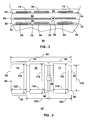
- FIG. 1 shows an exploded side view of a prior art three-layer capacitive accelerometer 20 constructed as a conventional hinged or "teeter-totter” type sensor.
- Capacitive accelerometer 20 includes a pair of static substrates 22 and 24, respectively, having opposed parallel planar faces.
- Substrates 22 and 24 are spaced from one another and each has a number of metal electrode elements 26 and 28 of a predetermined configuration deposited on one surface to form respective capacitor electrodes or "plates."
- electrode elements 26 operate as an excitation or sensing electrode to receive stimulating signals.
- the other electrode elements 28 operate as the feedback electrodes for electrostatic rebalance.
- a single set of electrode elements 26 (or 28) operates as both sensing and feedback electrodes when the feedback signal is superimposed on the sensing signal.
- a movable element 30, commonly referred to as a "proof mass,” is flexibly suspended between substrates 22 and 24 by one or more rotational flexures 32 situated at elevated attachment points 34 for rotation about a rotational axis 36 to form different sets of capacitors with electrodes 26 and 28.
- Movable element 30 moves in response to acceleration, thus changing its position relative to the static sensing electrodes 26. This change in position results in a set of capacitors whose difference, i.e., a differential capacitance, is indicative of acceleration.
- Another set of capacitors for electrostatic rebalance is made up of movable element 30 and feedback electrodes 28. Feedback electrodes 28 function to drive movable element 30 to its reference position balanced between the sensing elements 26 and maintain it there.
- first section 38 of movable element 30 on one side of rotational axis 36 is formed with relatively greater mass than a second section 40 of movable element 30 on the other side of rotational axis 36.
- the greater mass of first section 38 is typically created by offsetting rotational axis 36 such that an extended portion 42 of first section 38 is formed distal from rotational axis 36.
- electrode elements 26 and 28 are sized and spaced symmetrically with respect to the longitudinal axis, L, of movable element 30.
- electrode elements 26 and 28 are further sized and spaced symmetrically with respect to rotational axis 36.
- Two- and three-layer capacitive sensors having a teeter-totter configuration suffer from a number of drawbacks.
- the teeter-totter type capacitive accelerometer calls for a relatively large proof mass.
- a large proof mass requires more die area, hence increasing cost and package size.
- a proof mass should rotate as a rigid body. The propensity for a proof mass to deform or bend increases in relation to its increasing size, especially when it is subjected to high acceleration. This deformation or bending causes a non-linearity effect that results in decreased accuracy of the sensor.
- this nonlinearity can create DC offset in the sensor output and possibly cause dysfunction of the system in which the accelerometer is deployed.
- a smaller gap between the proof mass and the sensing electrodes or a thicker proof mass may mitigate the problem of deformation and the commensurate non-linearity effect.
- the manufacture of a smaller gap and/or a thicker proof mass leads to manufacturing issues.
- a problem particular to the three-layer teeter-totter configuration shown in FIG. 1 is that both the sensing electrodes 26 and the feedback electrodes 28 are clustered proximate rotational axis 36.
- This configuration is inefficient in that the surface area of extended portion 42, generally termed a shield area, of movable element 30 is unused.
- the surface areas of electrodes 26 and 28 are relatively small due to their clustered configuration about rotational axis 36.
- a smaller surface area of sensing electrodes 26 results in a lower capacitive output.
- a smaller surface area of feedback electrodes 28 provides insufficient actuation given voltage levels available from the feedback circuit (not shown).
- FIG. 1 shows an exploded side view of a prior art three-layer capacitive accelerometer 20 constructed as a conventional hinged or "teeter-totter” type sensor;
- FIG. 2 shows a perspective view of a differential capacitive sensor in accordance with the present invention
- FIG. 3 shows a highly enlarged cross-sectional view of a portion of the differential capacitive sensor during processing in accordance with the present invention
- FIG. 4 shows a top view of the differential capacitive sensor
- FIG. 5 shows a partial side view of the differential capacitive sensor
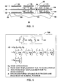
- FIG. 6 shows a table of a mathematical relationship between the capacitors of the differential capacitive sensor
- FIG. 7 shows a device in which the differential capacitive sensor may be installed.
- FIG. 2 shows a perspective view of a differential capacitive sensor 50 in accordance with the present invention.
- Sensor 50 may be, for example, a Micro Electro-Mechanical Systems (MEMS) accelerometer or other MEMS sensing device.
- MEMS Micro Electro-Mechanical Systems
- sensor 50 is referred to hereinafter as capacitive accelerometer 50.
- Capacitive accelerometer 50 is in a three-layer, teeter-totter configuration that provides more capacitive output than prior art devices, effectively cancels the non-linearity effect caused by non-rigid body deformation, and allows for sufficient electrostatic actuation that may be used for self test and/or for a "closed loop" or feedback design.
- Capacitive accelerometer 50 includes a first static conductive layer 52 disposed on a substrate 54. Another conductive layer, referred to herein as a movable element 56 is formed above first conductive layer 52. Movable element 56 is supported by a hinge element 58 and is allowed to pivot about a rotational axis 60 defined by hinge element 58. A second static conductive layer 62 is disposed above movable element 56. It should be understood that a number of flexures, hinges, and other rotational mechanisms may be utilized to enable pivotal movement of movable element 56 about rotational axis 60.
- First static conductive layer 52 is in the form of three electrically isolated electrodes or plates, including a first sensing electrode 64, a third sensing electrode 66, and a first actuation electrode 68.
- Second static conductive layer 62 is in the form of three electrically isolated plates or caps rigidly secured to substrate 54 and disposed over first conductive layer 52 and movable element 56.
- the caps include a second sensing electrode 70, a fourth sensing electrode 72, and a second actuation electrode 74. A portion of fourth sensing electrode 72 has been cut away to reveal hinge element 58 of movable element 56.
- FIG. 2 shows one possible configuration of differential accelerometer 50.
- the three-layers of differential accelerometer 50 can take on a number of forms that maintain each of first, second, third, and fourth sensing electrodes 64, 70, 66, and 72, as well as first and second actuation electrodes 68 and 74, electrically isolated from one another.
- FIG. 3 shows a highly enlarged cross-sectional view of a portion of differential accelerometer 50 during processing in accordance with the present invention.
- Substrate 54 may be a semiconductor wafer comprising silicon, although any mechanically supporting substrate may be utilized.
- An insulating layer 76 may be formed on the surface of substrate 54. Insulating layer 76 may be silicon dioxide, silicon nitride, and the like. Insulating layer 76 may be formed conformally and then patterned and etched. It functions to insulate first conductive layer 52 from substrate 54. It should be understood, however, that if substrate 54 is nonconductive, insulating layer 76 may not be utilized.
- First static conductive layer 52 comprises polysilicon, although other conductive materials may be employed.
- First conductive layer 52 may be formed by known methods such as deposition and sputtering.
- First conductive layer 52 may be deposited over the surface of substrate 54 as a blanket layer and can then be patterned and etched to form first sensing electrode 64, third sensing electrode 66, and first actuation electrode 68 of first conductive layer 52.
- a first protective layer 78 may optionally be disposed over first conductive layer 52 and patterned and etched as desired to protect substrate 54 during future processing steps and to prevent shorting and/or welding between first conductive layer 52 and movable element 56.
- a first sacrificial layer 80 may be formed on the patterned and etched first conductive layer 52. Like previous layers, first sacrificial layer 80 is also formed conformally and then patterned and etched as desired. First sacrificial layer 80 may be formed of phosphosilicate glass and can be deposited by chemical vapor deposition, as known to those skilled in the art. It should be understood that other sacrificial materials may be employed in lieu of phosphosilicate glass.
- the next conductive layer i.e., movable element 56, comprises polysilicon and is formed as a teeter-totter structure positioned over first conductive layer 52.
- Movable element 56 is mechanically attached to substrate 54 by hinge element 58.
- a second sacrificial layer 82 such as phosphosilicate glass, may be formed conformally on movable element 56 and then patterned and etched.
- a second protective layer 84 may optionally be formed on second sacrificial layer 82 to prevent shorting and/or welding between movable element 56 and second static conductive layer 62.
- Second static conductive layer 62 is formed on the patterned second sacrificial layer 82.
- Second conductive layer 62 also comprises polysilicon and is formed conformally and then patterned and etched accordingly to form second sensing electrode 70, fourth sensing electrode 72, and second actuation electrode 74.
- a protective layer 86 may be formed to protect second conductive layer 62.
- first and second sacrificial layers 80 and 82 are removed in accordance with conventional procedures.
- a selective etchant may be employed that can remove the phosphosilicate glass sacrificial layers without appreciably damaging the polysilicon of first static conductive layer 52, movable element 56, and second static conductive layer 62 or protective layers 78, 84, and 86.
- FIG. 4 shows a top view of the differential capacitive sensor, i.e., capacitive accelerometer 50.
- Movable element 56 underlies second sensing electrode 70, fourth sensing electrode 72, and second actuation electrode 74 of second static conductive layer 62.
- First sensing electrode 64, third sensing electrode 66, and first actuation electrode 68 of first static conductive layer 52 underlie movable element 56 and are not visible in FIG. 4 .
- Movable element 56 is adapted for motion relative to rotational axis 60 which is offset between a first end 88 and a second end 90 of movable element 56.
- Rotational axis 60 is oriented perpendicular to a longitudinal dimension 92 of movable element 56.
- a first section 94 of movable element 56 is formed between rotational axis 60 and first end 88, and a second section 96 of movable element 56 is formed between rotational axis 60 and second end 90.
- First section 94 of movable element 56 is formed with relatively greater mass than second section 96 by offsetting rotational axis 60 such that an extended portion 98 is formed distal from rotational axis 60.
- extended portion 98 of first section 94 is spaced away from rotational axis 60 at a distance 100 that is approximately equivalent to a length 102 of second section 96.
- FIG. 5 shows a partial side view of the differential capacitive sensor, i.e., capacitive accelerometer 50.
- Movable element 56 includes a first surface 104 and a second surface 106.
- First static conductive layer 52 is spaced away from first surface 104 of movable element 56 and second static conductive layer 62 is spaced away from second surface 106.
- First sensing electrode 64, third sensing electrode 66, and first actuation electrode 68 oppose first surface 104 of movable element 56.
- second sensing electrode 70, fourth sensing electrode 72, and second actuation electrode 74 oppose second surface 106 of movable element 56.
- first and second sensing electrodes 64 and 70 respectively, oppose opposite surfaces of first section 94 of movable element 56 in close proximity to rotational axis 60.
- third and fourth sensing electrodes 66 and 72 respectively, oppose opposite surfaces of second section 96 in close proximity to rotational axis 60.
- First sensing electrode 64 forms a first capacitor 108 with first section 94 of movable element 56
- third sensing electrode 66 forms a third capacitor 110 with second section 96 of movable element 56
- second sensing electrode 70 forms a second capacitor 112 with first section 94 of movable element 56
- fourth sensing electrode 72 forms a fourth capacitor 114 with second section 96 of movable element.
- First and third sensing electrodes 64 and 66 are symmetrically arranged relative to rotational axis 60
- second and fourth sensing electrodes 70 and 72 are symmetrically arranged relative to rotational axis 60.
- Each of electrodes 64, 66, 70, and 72 are generally equivalent in size and shape.
- First actuation electrode 68 is adjacent first sensing electrode 66, but is located distal from rotational axis 60 to oppose extended portion 98 of first section 94.
- second actuation electrode 74 is adjacent second sensing electrode 70, but is located distal from rotational axis 60 to oppose extended portion 98 of first section 94.
- First and second actuation electrodes 68 and 74, respectively, are advantageously incorporated into the unused shield area of unbalanced proof mass implementations without a commensurate increase in the die area of such a device.
- first and second actuation electrodes 68 and 74, respectively, at extended portion 98 allows for greater surface areas of electrodes 64, 66, 70, and 72, hence higher capacitive output of first, second, third, and fourth capacitors 108, 112, 110, and 114, respectively, over prior art designs.
- a surface area (i.e., a first dimension 116 multiplied by a second dimension 118) of each of electrodes 64, 66, 70, and 72 is in a range of approximately twenty-five to thirty-five percent of the overall surface area (i.e. length 92 multiplied by a width 120) of movable element 56 for desirable performance.
- each of the sensing electrodes on a given side of movable element 56 comprises a surface area in a range of twenty-five to thirty-five percent of an overall surface area of the given side of movable element 56.
- first and second actuation electrodes 68 and 74 at extended portion 98 also allows for relatively large surface areas of first and second actuation electrodes 68 and 74.
- a surface area i.e., a third dimension 122 multiplied by a fourth dimension 124
- a surface area i.e., a third dimension 122 multiplied by a fourth dimension 124 of each of first and second actuation electrodes 68 and 74, respectively, is in a range of approximately twenty to twenty-five percent of the overall surface area of movable element 56.
- Placement of first and second actuation electrodes 68 and 74 at extended portion is a desirable location for actuation because extended portion 98 is farther from rotational axis 60 and thus provides a large moment.
- First and second actuation electrodes 68 and 74 provide actuation for feedback "closed-loop" operation and/or for "self test” operation. For feedback operation, they provide ability to counteract large acceleration.
- a feedback signal can be applied to first and second electrodes 68 and 74 to sense the position of the movable element with capacitance and provide electrostatic bias to the actuation electrodes to keep the movable element stationary, or to restrict movement in certain frequency ranges. For example, movement may be restricted to allow high frequency movement but to counteract low-frequency movement, such as any temperature and/or time dependent offset caused by package stress.
- "self test” operation they can provide a large amount of actuation to test the function of differential accelerometer 50.
- the actuation is bi-directional, i.e. movable element 56 can be rotated in either direction.
- This configuration results in an efficient use of an entirety of the surface area of movable element 56. Moreover, this configuration allows for a smaller proof mass, i.e., movable element 56, while enabling significant capacitive output of capacitors 108, 112, 110, and 114 and allowing for a sufficient actuation voltage at first and second actuation electrodes 68 and 74, respectively.
- FIG. 6 shows a table 126 of a mathematical relationship between first, second, third, and fourth capacitors 108, 112, 110, and 114 of differential accelerometer 50 ( FIG. 2 ).
- An acceleration which causes movable element 56 ( FIG. 5 ) to pivot about rotational axis 60 so that first section 94 moves closer to first sensing element 64 and second section 96 moves closer to fourth sensing element 72 will result in a measured increase in both of first and fourth capacitors 108 and 114, respectively, and a measured decrease in both of second and third capacitors 112 and 110, respectively.
- a differential sense scheme is formed.
- differential accelerometer 50 provides about twice the base capacitance, C 0 , and about twice the delta capacitance, ⁇ C, under a given acceleration than a conventional two-layer teeter-totter configuration.
- this differential sense scheme cancels the second order nonlinear term found in two-layer teeter-totter designs caused by non-rigid proof mass deformation.
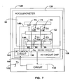
- FIG. 7 shows a device 128 in which differential accelerometer 50 may be installed.
- Device 128 can be any of a number of devices such as an inertial guidance system, an airbag deployment system in a vehicle, a protection system for a variety of devices, and many other scientific and engineering systems.
- Device 128 includes an accelerometer package 130 into which differential accelerometer 50 is incorporated.
- accelerometer package 130 is in communication with a circuit 132, which may include, for example, a processor, hard disk drive, and other components that are interconnected via conventional bus structures known to those skilled in the art.
- a circuit 132 which may include, for example, a processor, hard disk drive, and other components that are interconnected via conventional bus structures known to those skilled in the art.
- a circuit 132 which may include, for example, a processor, hard disk drive, and other components that are interconnected via conventional bus structures known to those skilled in the art.
- a circuit 132 which may include, for example, a processor, hard disk drive, and other components that are interconnected via
- circuit 132 monitors signals from accelerometer package 130. These signals include acceleration along the Z axis.
- Differential accelerometer 50 of accelerometer package 130 senses a Z axis acceleration (A z ) 136.
- Z axis acceleration 136 is produced by capacitances from first, second, third, and fourth capacitors 108, 112, 110, and 114 as discussed in connection with FIG. 6 .
- the capacitance signals from differential accelerometer 50 are communicated to a sense circuit of an input/output circuit chip 138 for suitable processing, as known to those skilled in the art, prior to output to circuit 132.
- Accelerometer package 130 further includes an actuation voltage input port 140 in communication with circuit 132 for application of a digital input voltage signal 142.
- Voltage signal 142 signals an actuation circuit 144 of I/O circuit chip 138 to provide an actuation voltage (V+ and V-) 146 at first and second actuation electrodes 68 and 74, respectively.
- actuation voltage 146 is a feedback voltage. The feedback voltage can be applied to first and second electrodes 68 and 74 to cancel any temperature and/or time dependent offset caused by package stress such that a position of movable element 52 is substantially constant.
- actuation voltage may be a self test voltage when accelerometer package 130 is placed in a self test mode.
- a self test voltage can be applied to first and second actuation electrodes 68 and 74 to test the function of differential accelerometer 50.
- Circuit 132 may additionally be in communication with a port (not shown) external to device 128 so that an external input signal may be communicated to circuit 132.
- Processor software or hardware on circuit 132 subsequently generates voltage signal 142, which is conveyed to input port 140.
- An embodiment described herein comprises a device that includes a differential capacitive sensor.
- Another embodiment comprises a method of fabricating the micro electro-mechanical systems differential capacitive sensor of the present invention.
- the sensor may be a differential accelerometer fabricated as a three-layer teeter-totter structure. Actuation electrodes are placed distal from the rotational axis of the teeter-totter structure so that relatively large sensing electrodes can be clustered proximate the rotational axis. In addition, relatively large actuation electrodes are positioned distal from the rotational axis of the movable element to take advantage of a large moment arm of the movable element.
- sensing electrodes and feedback electrodes allows for the utilization of a smaller movable element (i.e., proof mass) that can be used to design a smaller package, lower cost sensor having sufficient capacitance and/or signal level. This smaller sensor will have less proof mass deformation, thus greater accuracy.
- the three-layer teeter-totter structure can also be used with feedback "closed loop" systems to sense the position of the movable element with capacitance and to provide electrostatic bias to the actuation electrodes to effectively cancel the non-linearity effect caused by non-rigid body deformation, and/or to provide sufficient electrostatic actuation for self test operation.
- first and second actuation electrodes may be utilized as sensing electrodes in applications where no actuation is required. Under such a situation, the amount of capacitance output can be correspondingly increased.
Description
- The present invention relates generally to micro electro-mechanical systems (MEMS) sensors. More specifically, the present invention relates to a MEMS differential capacitive accelerometer.
- An accelerometer is a sensor typically utilized for measuring acceleration forces. These forces may be static, like the constant force of gravity, or they can be dynamic, caused by moving or vibrating the accelerometer. An accelerometer may sense acceleration or other phenomena along one, two, or three axes or directions. From this information, the movement or orientation of the device in which the accelerometer is installed can be ascertained. Accelerometers are used in inertial guidance systems, in airbag deployment systems in vehicles, in protection systems for a variety of devices, and many other scientific and engineering systems.
- Capacitive-sensing MEMS accelerometer designs are highly desirable for operation in high gravity environments and in miniaturized devices, and due to their relatively low cost. Capacitive accelerometers sense a change in electrical capacitance, with respect to acceleration, to vary the output of an energized circuit. One common form of accelerometer is a two layer capacitive transducer having a "teeter-totter" or "see saw" configuration. This commonly utilized transducer type uses a movable element or plate that rotates under z-axis acceleration above a substrate. The accelerometer structure can measure two distinct capacitances to determine differential or relative capacitance.
-
US-A-2004/0160232 discloses a capacitive acceleration sensing device having a movable element suspended between static electrodes.FR-A- 2 694 403 FIG. 1 shows an exploded side view of a prior art three-layercapacitive accelerometer 20 constructed as a conventional hinged or "teeter-totter" type sensor.Capacitive accelerometer 20 includes a pair ofstatic substrates Substrates metal electrode elements electrode elements 26 operate as an excitation or sensing electrode to receive stimulating signals. Theother electrode elements 28 operate as the feedback electrodes for electrostatic rebalance. A single set of electrode elements 26 (or 28) operates as both sensing and feedback electrodes when the feedback signal is superimposed on the sensing signal. - A
movable element 30, commonly referred to as a "proof mass," is flexibly suspended betweensubstrates rotational flexures 32 situated at elevatedattachment points 34 for rotation about arotational axis 36 to form different sets of capacitors withelectrodes Movable element 30 moves in response to acceleration, thus changing its position relative to thestatic sensing electrodes 26. This change in position results in a set of capacitors whose difference, i.e., a differential capacitance, is indicative of acceleration. Another set of capacitors for electrostatic rebalance is made up ofmovable element 30 andfeedback electrodes 28.Feedback electrodes 28 function to drivemovable element 30 to its reference position balanced between thesensing elements 26 and maintain it there. - When intended for operation as a teeter-totter type accelerometer, a
first section 38 ofmovable element 30 on one side ofrotational axis 36 is formed with relatively greater mass than asecond section 40 ofmovable element 30 on the other side ofrotational axis 36. The greater mass offirst section 38 is typically created by offsettingrotational axis 36 such that an extendedportion 42 offirst section 38 is formed distal fromrotational axis 36. In addition,electrode elements movable element 30. Similarly,electrode elements rotational axis 36. - Two- and three-layer capacitive sensors having a teeter-totter configuration suffer from a number of drawbacks. In order to provide more capacitive output and hence better circuit performance (e.g., lower noise) the teeter-totter type capacitive accelerometer calls for a relatively large proof mass. Unfortunately, a large proof mass requires more die area, hence increasing cost and package size. Moreover, a proof mass should rotate as a rigid body. The propensity for a proof mass to deform or bend increases in relation to its increasing size, especially when it is subjected to high acceleration. This deformation or bending causes a non-linearity effect that results in decreased accuracy of the sensor. For example, this nonlinearity can create DC offset in the sensor output and possibly cause dysfunction of the system in which the accelerometer is deployed. A smaller gap between the proof mass and the sensing electrodes or a thicker proof mass may mitigate the problem of deformation and the commensurate non-linearity effect. However, the manufacture of a smaller gap and/or a thicker proof mass leads to manufacturing issues.
- A problem particular to the three-layer teeter-totter configuration shown in
FIG. 1 is that both thesensing electrodes 26 and thefeedback electrodes 28 are clustered proximaterotational axis 36. This configuration is inefficient in that the surface area of extendedportion 42, generally termed a shield area, ofmovable element 30 is unused. Moreover, the surface areas ofelectrodes rotational axis 36. A smaller surface area ofsensing electrodes 26 results in a lower capacitive output. A smaller surface area offeedback electrodes 28 provides insufficient actuation given voltage levels available from the feedback circuit (not shown). - A more complete understanding of the present invention may be derived by referring to the detailed description and claims when considered in connection with the Figures, wherein like reference numbers refer to similar items throughout the Figures, and:
-
FIG. 1 shows an exploded side view of a prior art three-layercapacitive accelerometer 20 constructed as a conventional hinged or "teeter-totter" type sensor; -
FIG. 2 shows a perspective view of a differential capacitive sensor in accordance with the present invention; -
FIG. 3 shows a highly enlarged cross-sectional view of a portion of the differential capacitive sensor during processing in accordance with the present invention; -
FIG. 4 shows a top view of the differential capacitive sensor; -
FIG. 5 shows a partial side view of the differential capacitive sensor; -
FIG. 6 shows a table of a mathematical relationship between the capacitors of the differential capacitive sensor; and -
FIG. 7 shows a device in which the differential capacitive sensor may be installed. -
FIG. 2 shows a perspective view of a differentialcapacitive sensor 50 in accordance with the present invention.Sensor 50 may be, for example, a Micro Electro-Mechanical Systems (MEMS) accelerometer or other MEMS sensing device. For purposes of the following discussion,sensor 50 is referred to hereinafter ascapacitive accelerometer 50.Capacitive accelerometer 50 is in a three-layer, teeter-totter configuration that provides more capacitive output than prior art devices, effectively cancels the non-linearity effect caused by non-rigid body deformation, and allows for sufficient electrostatic actuation that may be used for self test and/or for a "closed loop" or feedback design. -
Capacitive accelerometer 50 includes a first staticconductive layer 52 disposed on asubstrate 54. Another conductive layer, referred to herein as amovable element 56 is formed above firstconductive layer 52.Movable element 56 is supported by ahinge element 58 and is allowed to pivot about arotational axis 60 defined byhinge element 58. A second staticconductive layer 62 is disposed abovemovable element 56. It should be understood that a number of flexures, hinges, and other rotational mechanisms may be utilized to enable pivotal movement ofmovable element 56 aboutrotational axis 60. - First static
conductive layer 52 is in the form of three electrically isolated electrodes or plates, including afirst sensing electrode 64, athird sensing electrode 66, and afirst actuation electrode 68. Second staticconductive layer 62 is in the form of three electrically isolated plates or caps rigidly secured tosubstrate 54 and disposed over firstconductive layer 52 andmovable element 56. The caps include asecond sensing electrode 70, afourth sensing electrode 72, and asecond actuation electrode 74. A portion offourth sensing electrode 72 has been cut away to revealhinge element 58 ofmovable element 56. -
FIG. 2 shows one possible configuration ofdifferential accelerometer 50. However, it should be understood that the three-layers ofdifferential accelerometer 50 can take on a number of forms that maintain each of first, second, third, andfourth sensing electrodes second actuation electrodes -
FIG. 3 shows a highly enlarged cross-sectional view of a portion ofdifferential accelerometer 50 during processing in accordance with the present invention.Substrate 54 may be a semiconductor wafer comprising silicon, although any mechanically supporting substrate may be utilized. An insulatinglayer 76 may be formed on the surface ofsubstrate 54. Insulatinglayer 76 may be silicon dioxide, silicon nitride, and the like. Insulatinglayer 76 may be formed conformally and then patterned and etched. It functions to insulate firstconductive layer 52 fromsubstrate 54. It should be understood, however, that ifsubstrate 54 is nonconductive, insulatinglayer 76 may not be utilized. - First static
conductive layer 52 comprises polysilicon, although other conductive materials may be employed. Firstconductive layer 52 may be formed by known methods such as deposition and sputtering. Firstconductive layer 52 may be deposited over the surface ofsubstrate 54 as a blanket layer and can then be patterned and etched to formfirst sensing electrode 64,third sensing electrode 66, andfirst actuation electrode 68 of firstconductive layer 52. A firstprotective layer 78 may optionally be disposed over firstconductive layer 52 and patterned and etched as desired to protectsubstrate 54 during future processing steps and to prevent shorting and/or welding between firstconductive layer 52 andmovable element 56. - A first
sacrificial layer 80 may be formed on the patterned and etched firstconductive layer 52. Like previous layers, firstsacrificial layer 80 is also formed conformally and then patterned and etched as desired. Firstsacrificial layer 80 may be formed of phosphosilicate glass and can be deposited by chemical vapor deposition, as known to those skilled in the art. It should be understood that other sacrificial materials may be employed in lieu of phosphosilicate glass. - The next conductive layer, i.e.,
movable element 56, comprises polysilicon and is formed as a teeter-totter structure positioned over firstconductive layer 52.Movable element 56 is mechanically attached tosubstrate 54 byhinge element 58. A secondsacrificial layer 82, such as phosphosilicate glass, may be formed conformally onmovable element 56 and then patterned and etched. A secondprotective layer 84 may optionally be formed on secondsacrificial layer 82 to prevent shorting and/or welding betweenmovable element 56 and second staticconductive layer 62. - Second static
conductive layer 62 is formed on the patterned secondsacrificial layer 82. Secondconductive layer 62 also comprises polysilicon and is formed conformally and then patterned and etched accordingly to formsecond sensing electrode 70,fourth sensing electrode 72, andsecond actuation electrode 74. Following the formation of second staticconductive layer 62, aprotective layer 86 may be formed to protect secondconductive layer 62. - Following the formation of the above described structure, first and second
sacrificial layers conductive layer 52,movable element 56, and second staticconductive layer 62 orprotective layers -
FIG. 4 shows a top view of the differential capacitive sensor, i.e.,capacitive accelerometer 50.Movable element 56 underliessecond sensing electrode 70,fourth sensing electrode 72, andsecond actuation electrode 74 of second staticconductive layer 62.First sensing electrode 64,third sensing electrode 66, andfirst actuation electrode 68 of first staticconductive layer 52 underliemovable element 56 and are not visible inFIG. 4 . -
Movable element 56 is adapted for motion relative torotational axis 60 which is offset between afirst end 88 and asecond end 90 ofmovable element 56.Rotational axis 60 is oriented perpendicular to alongitudinal dimension 92 ofmovable element 56. Afirst section 94 ofmovable element 56 is formed betweenrotational axis 60 andfirst end 88, and asecond section 96 ofmovable element 56 is formed betweenrotational axis 60 andsecond end 90.First section 94 ofmovable element 56 is formed with relatively greater mass thansecond section 96 by offsettingrotational axis 60 such that anextended portion 98 is formed distal fromrotational axis 60. In one embodiment,extended portion 98 offirst section 94 is spaced away fromrotational axis 60 at adistance 100 that is approximately equivalent to alength 102 ofsecond section 96. - Referring to
FIGs. 4-5 ,FIG. 5 shows a partial side view of the differential capacitive sensor, i.e.,capacitive accelerometer 50.Movable element 56 includes afirst surface 104 and asecond surface 106. First staticconductive layer 52 is spaced away fromfirst surface 104 ofmovable element 56 and second staticconductive layer 62 is spaced away fromsecond surface 106. -
First sensing electrode 64,third sensing electrode 66, andfirst actuation electrode 68 opposefirst surface 104 ofmovable element 56. Similarly,second sensing electrode 70,fourth sensing electrode 72, andsecond actuation electrode 74 opposesecond surface 106 ofmovable element 56. More particularly, first andsecond sensing electrodes first section 94 ofmovable element 56 in close proximity torotational axis 60. Similarly, third andfourth sensing electrodes second section 96 in close proximity torotational axis 60. -
First sensing electrode 64 forms afirst capacitor 108 withfirst section 94 ofmovable element 56, andthird sensing electrode 66 forms athird capacitor 110 withsecond section 96 ofmovable element 56. In addition,second sensing electrode 70 forms asecond capacitor 112 withfirst section 94 ofmovable element 56 andfourth sensing electrode 72 forms afourth capacitor 114 withsecond section 96 of movable element. - First and
third sensing electrodes rotational axis 60, and second andfourth sensing electrodes rotational axis 60. Each ofelectrodes First actuation electrode 68 is adjacentfirst sensing electrode 66, but is located distal fromrotational axis 60 to oppose extendedportion 98 offirst section 94. Likewise,second actuation electrode 74 is adjacentsecond sensing electrode 70, but is located distal fromrotational axis 60 to oppose extendedportion 98 offirst section 94. First andsecond actuation electrodes - Placement of first and
second actuation electrodes extended portion 98 allows for greater surface areas ofelectrodes fourth capacitors first dimension 116 multiplied by a second dimension 118) of each ofelectrodes length 92 multiplied by a width 120) ofmovable element 56 for desirable performance. Since there are two sensing electrodes on each side ofmovable element 56, approximately fifty to seventy percent of each of first andsecond surfaces respective sensing electrodes movable element 56 comprises a surface area in a range of twenty-five to thirty-five percent of an overall surface area of the given side ofmovable element 56. - In addition, the placement of first and
second actuation electrodes extended portion 98 also allows for relatively large surface areas of first andsecond actuation electrodes third dimension 122 multiplied by a fourth dimension 124) of each of first andsecond actuation electrodes movable element 56. Placement of first andsecond actuation electrodes extended portion 98 is farther fromrotational axis 60 and thus provides a large moment. - First and
second actuation electrodes second electrodes differential accelerometer 50. Moreover in both cases, the actuation is bi-directional, i.e.movable element 56 can be rotated in either direction. - This configuration results in an efficient use of an entirety of the surface area of
movable element 56. Moreover, this configuration allows for a smaller proof mass, i.e.,movable element 56, while enabling significant capacitive output ofcapacitors second actuation electrodes -
FIG. 6 shows a table 126 of a mathematical relationship between first, second, third, andfourth capacitors FIG. 2 ). An acceleration which causes movable element 56 (FIG. 5 ) to pivot aboutrotational axis 60 so thatfirst section 94 moves closer tofirst sensing element 64 andsecond section 96 moves closer tofourth sensing element 72 will result in a measured increase in both of first andfourth capacitors third capacitors fourth capacitors third capacitors differential accelerometer 50 provides about twice the base capacitance, C0, and about twice the delta capacitance, ΔC, under a given acceleration than a conventional two-layer teeter-totter configuration. In addition, this differential sense scheme cancels the second order nonlinear term found in two-layer teeter-totter designs caused by non-rigid proof mass deformation. -
FIG. 7 shows adevice 128 in whichdifferential accelerometer 50 may be installed.Device 128 can be any of a number of devices such as an inertial guidance system, an airbag deployment system in a vehicle, a protection system for a variety of devices, and many other scientific and engineering systems.Device 128 includes anaccelerometer package 130 into whichdifferential accelerometer 50 is incorporated. In this exemplary situation,accelerometer package 130 is in communication with acircuit 132, which may include, for example, a processor, hard disk drive, and other components that are interconnected via conventional bus structures known to those skilled in the art. Those skilled in the art will recognize thatdevice 128 may include many other components that are not discussed herein for brevity. Furthermore,device 128 need not have the structures specified herein. - In general,
circuit 132 monitors signals fromaccelerometer package 130. These signals include acceleration along the Z axis.Differential accelerometer 50 ofaccelerometer package 130 senses a Z axis acceleration (Az) 136. In accordance with the present invention,Z axis acceleration 136 is produced by capacitances from first, second, third, andfourth capacitors FIG. 6 . The capacitance signals fromdifferential accelerometer 50 are communicated to a sense circuit of an input/output circuit chip 138 for suitable processing, as known to those skilled in the art, prior to output tocircuit 132. -
Accelerometer package 130 further includes an actuationvoltage input port 140 in communication withcircuit 132 for application of a digitalinput voltage signal 142.Voltage signal 142 signals anactuation circuit 144 of I/O circuit chip 138 to provide an actuation voltage (V+ and V-) 146 at first andsecond actuation electrodes differential accelerometer 50 is configured as a "closed loop" design,actuation voltage 146 is a feedback voltage. The feedback voltage can be applied to first andsecond electrodes movable element 52 is substantially constant. Alternatively, actuation voltage may be a self test voltage whenaccelerometer package 130 is placed in a self test mode. A self test voltage can be applied to first andsecond actuation electrodes differential accelerometer 50.Circuit 132 may additionally be in communication with a port (not shown) external todevice 128 so that an external input signal may be communicated tocircuit 132. Processor software or hardware oncircuit 132 subsequently generatesvoltage signal 142, which is conveyed to inputport 140. - An embodiment described herein comprises a device that includes a differential capacitive sensor. Another embodiment comprises a method of fabricating the micro electro-mechanical systems differential capacitive sensor of the present invention. The sensor may be a differential accelerometer fabricated as a three-layer teeter-totter structure. Actuation electrodes are placed distal from the rotational axis of the teeter-totter structure so that relatively large sensing electrodes can be clustered proximate the rotational axis. In addition, relatively large actuation electrodes are positioned distal from the rotational axis of the movable element to take advantage of a large moment arm of the movable element. The configuration of sensing electrodes and feedback electrodes allows for the utilization of a smaller movable element (i.e., proof mass) that can be used to design a smaller package, lower cost sensor having sufficient capacitance and/or signal level. This smaller sensor will have less proof mass deformation, thus greater accuracy. The three-layer teeter-totter structure can also be used with feedback "closed loop" systems to sense the position of the movable element with capacitance and to provide electrostatic bias to the actuation electrodes to effectively cancel the non-linearity effect caused by non-rigid body deformation, and/or to provide sufficient electrostatic actuation for self test operation.
- Although the preferred embodiments of the invention have been illustrated and described in detail, it will be readily apparent to those skilled in the art that various modifications may be made therein without departing from the spirit of the invention or from the scope of the appended claims. For example, the first and second actuation electrodes may be utilized as sensing electrodes in applications where no actuation is required. Under such a situation, the amount of capacitance output can be correspondingly increased.
Claims (14)
- A device (128) comprising:a Micro Electro-Mechanical System (MEMS) sensor (50), said sensor (50) comprising:a movable element (56), said movable element (56) including a first surface (104) and a second surface (106);a first static conductive layer (52) spaced away from said first surface (104) of said movable element (56), anda second static conductive layer (62) spaced away from said second surface (106) of said movable element (56),characterised in that;said movable element (56) is adapted for motion relative to a rotational axis (60) offset between first and second ends (88, 90) thereof to form a first section (94) between said rotational axis (60) and said first end (88) and a second section (96) between said rotational axis (60) and said second end (90), said first section (94) including an extended portion (98) spaced away from said rotational axis (60) at a distance (100) approximately equivalent to a length (102) of said second section (96) between said rotational axis (60) and said second end (90), and in thatsaid first conductive layer (52) includes a first actuation electrode (68) and a first sensing electrode (64) andsaid second conductive layer (62) includes a second actuation electrode (74) and a second sensing electrode (70),said first and second actuation electrodes (68, 74) opposing said extended portion (98).
- A device (128) as claimed in claim 1 wherein:said first and second sensing electrodes (64, 70) oppose said first section (94) of said movable element (56);said first conductive layer (52) includes a third sensing electrode (66); andsaid second conductive layer (62) includes a fourth sensing electrode (72), said third and fourth sensing electrodes (66, 72) opposing said second section (96) of said movable element (56).
- A device (128) as claimed in claim 2 wherein each of said third and fourth sensing electrodes (66, 72) has a surface area in a range of twenty-five to thirty-five percent of an overall surface area of said movable element (56).
- A device (128) as claimed in claim 2 wherein:said first and third sensing electrodes (64, 66) are symmetrically arranged relative to said rotational axis (60); andsaid second and fourth sensing electrodes (70, 72) are symmetrically arranged relative to said rotational axis (60).
- A device (128) as claimed in claim 2 wherein:said first and third sensing electrodes (64, 66) form respective first and third capacitors (108, 110) with said first and second sections (94, 96) of said movable element (56); andsaid second and fourth sensing electrodes (70, 72) form respective second and fourth capacitors (112, 114) with said first and second sections (94, 96) of said movable element (56).
- A device (128) as claimed in claim 1 wherein:said first and second sensing electrodes (64, 70) oppose said first section (94) of said movable element (56);said first actuation electrode (68) is adjacent to said first sensing electrode (64); andsaid second actuation electrode (74) is adjacent to said second sensing electrode (70).
- A device (128) as claimed in claim 6 wherein:said first actuation electrode (68) is electrically isolated from said first sensing electrode (64); andsaid second actuation electrode (74) is electrically isolated from said second sensing electrode (70).
- A device (128) as claimed in claim 1 wherein a surface area of each of said first and second actuation electrodes (68, 74) is in a range of twenty to twenty-five percent of an overall surface area of said movable element (56).
- A device (128) as claimed in claim 1 wherein voltage (146) is applied to said first and second actuation electrodes (68, 74) to test said sensor (50).
- A device (128) as claimed in claim 1 wherein voltage (146) is applied to said first and second actuation electrodes (68, 74) to provide a balance force such that a position of said movable element (56) is substantially constant.
- A device (128) as claimed in claim 1 wherein said first and second sensing electrodes (64, 70) are adapted to detect movement (136) of said movable element (56) along an axis perpendicular to a plane of said electrodes (64, 70).
- A device (128) as claimed in claim 1 wherein:said first static conductive layer (52 further includes_a third sensing electrode (66); andsaid second static conductive layer (62 further includes a fourth sensing electrode (72); and said first and second sensing electrodes (64, 70) opposes said first section (94), said third and fourth sensing electrodes (66, 72) opposes said second section (96), and each of said first, second, third, and fourth sensing electrodes (64, 70, 66, 72) have a surface area in a range of twenty-five to thirty-five percent of an overall surface area of said movable element (56).
- A device (128)_as claimed in claim 12 wherein each of said first and second actuation electrodes (68, 74) has a second surface area in a range of twenty to twenty-five percent of an overall surface area of said movable element (56).
- A device (128) as claimed in claim 12 wherein:said first and third sensing electrodes (64, 66) are symmetrically arranged relative to said rotational axis (60); andsaid second and fourth sensing electrodes (70, 72) are symmetrically arranged relative to said rotational axis (60).
Applications Claiming Priority (2)
| Application Number | Priority Date | Filing Date | Title |
|---|---|---|---|
| US11/655,557 US7610809B2 (en) | 2007-01-18 | 2007-01-18 | Differential capacitive sensor and method of making same |
| PCT/US2007/087846 WO2008088644A1 (en) | 2007-01-18 | 2007-12-18 | Differential capacitive sensor and method of making same |
Publications (3)
| Publication Number | Publication Date |
|---|---|
| EP2106553A1 EP2106553A1 (en) | 2009-10-07 |
| EP2106553A4 EP2106553A4 (en) | 2011-11-30 |
| EP2106553B1 true EP2106553B1 (en) | 2012-11-14 |
Family
ID=39636279
Family Applications (1)
| Application Number | Title | Priority Date | Filing Date |
|---|---|---|---|
| EP07869403A Not-in-force EP2106553B1 (en) | 2007-01-18 | 2007-12-18 | Differential capacitive sensor and method of making same |
Country Status (5)
| Country | Link |
|---|---|
| US (1) | US7610809B2 (en) |
| EP (1) | EP2106553B1 (en) |
| JP (1) | JP5794601B2 (en) |
| TW (1) | TWI449914B (en) |
| WO (1) | WO2008088644A1 (en) |
Families Citing this family (48)
| Publication number | Priority date | Publication date | Assignee | Title |
|---|---|---|---|---|
| FR2921916B1 (en) * | 2007-10-09 | 2011-04-29 | Commissariat Energie Atomique | NANOMETRIC OR MICROMETRIC VIBRANT ELECTROMECHANICAL COMPONENT WITH INCREASED DETECTION LEVEL |
| DE102008017156A1 (en) * | 2008-04-03 | 2009-10-08 | Continental Teves Ag & Co. Ohg | Micromechanical acceleration sensor |
| DE102009021567A1 (en) * | 2008-05-15 | 2009-12-31 | Continental Teves Ag & Co. Ohg | Micromechanical acceleration sensor |
| US8499629B2 (en) | 2008-10-10 | 2013-08-06 | Honeywell International Inc. | Mounting system for torsional suspension of a MEMS device |
| US8020443B2 (en) * | 2008-10-30 | 2011-09-20 | Freescale Semiconductor, Inc. | Transducer with decoupled sensing in mutually orthogonal directions |
| DE102008043790B4 (en) * | 2008-11-17 | 2017-04-06 | Robert Bosch Gmbh | Micromechanical component |
| DE102009026462B4 (en) * | 2009-05-26 | 2023-03-30 | Robert Bosch Gmbh | accelerometer |
| DE102009029248B4 (en) * | 2009-09-08 | 2022-12-15 | Robert Bosch Gmbh | Micromechanical system for detecting an acceleration |
| US8839670B2 (en) * | 2010-11-24 | 2014-09-23 | Invensense, Inc. | Anchor-tilt cancelling accelerometer |
| CN103779142B (en) * | 2010-12-31 | 2017-06-06 | 上海丽恒光微电子科技有限公司 | Gate |
| US8927311B2 (en) | 2011-02-16 | 2015-01-06 | Freescale Semiconductor, Inc. | MEMS device having variable gap width and method of manufacture |
| US9069005B2 (en) * | 2011-06-17 | 2015-06-30 | Avago Technologies General Ip (Singapore) Pte. Ltd. | Capacitance detector for accelerometer and gyroscope and accelerometer and gyroscope with capacitance detector |
| JP5790296B2 (en) * | 2011-08-17 | 2015-10-07 | セイコーエプソン株式会社 | Physical quantity sensor and electronic equipment |
| US10371714B2 (en) | 2012-06-14 | 2019-08-06 | Analog Devices, Inc. | Teeter-totter type MEMS accelerometer with electrodes on circuit wafer |
| US9046547B2 (en) * | 2012-08-13 | 2015-06-02 | Pgs Geophysical As | Accelerometer having multiple feedback systems operating on a given proof mass |
| US9134337B2 (en) * | 2012-12-17 | 2015-09-15 | Maxim Integrated Products, Inc. | Microelectromechanical z-axis out-of-plane stopper |
| US9470709B2 (en) | 2013-01-28 | 2016-10-18 | Analog Devices, Inc. | Teeter totter accelerometer with unbalanced mass |
| US9190937B2 (en) | 2013-02-06 | 2015-11-17 | Freescale Semiconductor, Inc. | Stiction resistant mems device and method of operation |
| US9297825B2 (en) | 2013-03-05 | 2016-03-29 | Analog Devices, Inc. | Tilt mode accelerometer with improved offset and noise performance |
| US20140260617A1 (en) | 2013-03-14 | 2014-09-18 | Agency For Science Technology And Research (A*Star) | Fully differential capacitive architecture for mems accelerometer |
| US20140260618A1 (en) * | 2013-03-14 | 2014-09-18 | Agency For Science Technology And Research (A*Star) | Force feedback electrodes in mems accelerometer |
| US9383384B2 (en) * | 2013-05-31 | 2016-07-05 | Honeywell International Inc. | Extended-range closed-loop accelerometer |
| US9556017B2 (en) | 2013-06-25 | 2017-01-31 | Analog Devices, Inc. | Apparatus and method for preventing stiction of MEMS devices encapsulated by active circuitry |
| US10081535B2 (en) | 2013-06-25 | 2018-09-25 | Analog Devices, Inc. | Apparatus and method for shielding and biasing in MEMS devices encapsulated by active circuitry |
| US9335340B2 (en) * | 2013-07-23 | 2016-05-10 | Freescale Semiconductor, Inc. | MEMS parameter identification using modulated waveforms |
| US9242851B2 (en) | 2013-08-06 | 2016-01-26 | Freescale Semiconductor, Inc | MEMS device with differential vertical sense electrodes |
| JP6146565B2 (en) * | 2013-08-06 | 2017-06-14 | セイコーエプソン株式会社 | Physical quantity sensors, electronic devices, and moving objects |
| US9927459B2 (en) | 2013-11-06 | 2018-03-27 | Analog Devices, Inc. | Accelerometer with offset compensation |
| US8893563B1 (en) * | 2014-01-15 | 2014-11-25 | King Fahd University Of Petroleum And Minerals | Differential capacitance torque sensor |
| JP6413463B2 (en) * | 2014-08-15 | 2018-10-31 | セイコーエプソン株式会社 | Physical quantity sensor, physical quantity sensor device, electronic device and mobile object |
| JP6655281B2 (en) * | 2014-08-19 | 2020-02-26 | セイコーエプソン株式会社 | Physical quantity sensors, electronic devices and moving objects |
| JP6358913B2 (en) * | 2014-09-30 | 2018-07-18 | 株式会社日立製作所 | Acceleration sensor |
| JP6262629B2 (en) * | 2014-09-30 | 2018-01-17 | 株式会社日立製作所 | Inertial sensor |
| US10203351B2 (en) | 2014-10-03 | 2019-02-12 | Analog Devices, Inc. | MEMS accelerometer with Z axis anchor tracking |
| US9604841B2 (en) | 2014-11-06 | 2017-03-28 | Analog Devices, Inc. | MEMS sensor cap with multiple isolated electrodes |
| US10527642B2 (en) | 2014-11-11 | 2020-01-07 | Hitachi, Ltd. | Acceleration sensor |
| US10073113B2 (en) | 2014-12-22 | 2018-09-11 | Analog Devices, Inc. | Silicon-based MEMS devices including wells embedded with high density metal |
| US10078098B2 (en) | 2015-06-23 | 2018-09-18 | Analog Devices, Inc. | Z axis accelerometer design with offset compensation |
| JP6631108B2 (en) * | 2015-09-15 | 2020-01-15 | セイコーエプソン株式会社 | Physical quantity sensors, sensor devices, electronic devices and moving objects |
| JP6437429B2 (en) * | 2015-12-25 | 2018-12-12 | 株式会社日立製作所 | Accelerometer, geophone and seismic exploration system |
| US10203352B2 (en) | 2016-08-04 | 2019-02-12 | Analog Devices, Inc. | Anchor tracking apparatus for in-plane accelerometers and related methods |
| US10261105B2 (en) | 2017-02-10 | 2019-04-16 | Analog Devices, Inc. | Anchor tracking for MEMS accelerometers |
| TWI668412B (en) | 2017-05-08 | 2019-08-11 | 日商村田製作所股份有限公司 | Capacitive microelectromechanical accelerometer and associated method |
| US10816568B2 (en) | 2017-12-26 | 2020-10-27 | Physical Logic Ltd. | Closed loop accelerometer |
| JP2021021676A (en) * | 2019-07-30 | 2021-02-18 | セイコーエプソン株式会社 | Inertia sensor, electronic apparatus, and moving body |
| CN113325200B (en) * | 2020-02-28 | 2024-04-05 | 精工爱普生株式会社 | Physical quantity sensor, electronic device, and moving object |
| US20220276615A1 (en) * | 2021-02-26 | 2022-09-01 | Honeywell International Inc. | Thermal metamaterial for low power mems thermal control |
| EP4123313A1 (en) * | 2021-07-23 | 2023-01-25 | STMicroelectronics S.r.l. | Closed-loop microelectromechanical accelerometer with compensation of spurious vibration modes and process for manufacturing a microelectromechanical accelerometer |
Family Cites Families (21)
| Publication number | Priority date | Publication date | Assignee | Title |
|---|---|---|---|---|
| US4736629A (en) * | 1985-12-20 | 1988-04-12 | Silicon Designs, Inc. | Micro-miniature accelerometer |
| US4987779A (en) * | 1989-02-28 | 1991-01-29 | United Technologies Corporation | Pulse-driven accelerometer arrangement |
| US5146389A (en) * | 1991-07-22 | 1992-09-08 | Motorola, Inc. | Differential capacitor structure and method |
| US5181156A (en) * | 1992-05-14 | 1993-01-19 | Motorola Inc. | Micromachined capacitor structure and method for making |
| FR2694403B1 (en) * | 1992-07-31 | 1994-10-07 | Sagem | Pendulum electrostatic accelerometer with test electrode and method of manufacturing such an accelerometer. |
| US5433101A (en) * | 1993-07-12 | 1995-07-18 | Ford Motor Company | Method and apparatus for self-testing a single-point automotive impact sensing system |
| US5587518A (en) * | 1994-12-23 | 1996-12-24 | Ford Motor Company | Accelerometer with a combined self-test and ground electrode |
| DE19541388A1 (en) * | 1995-11-07 | 1997-05-15 | Telefunken Microelectron | Micromechanical acceleration sensor |
| JPH1123611A (en) * | 1997-07-09 | 1999-01-29 | Japan Aviation Electron Ind Ltd | Electrostatic torquer type accelerometer |
| JP3371250B2 (en) * | 1999-09-06 | 2003-01-27 | 日本航空電子工業株式会社 | Electrostatic Toluca type accelerometer |
| US6230566B1 (en) * | 1999-10-01 | 2001-05-15 | The Regents Of The University Of California | Micromachined low frequency rocking accelerometer with capacitive pickoff |
| JP2003248016A (en) * | 2002-02-21 | 2003-09-05 | Denso Corp | Capacitance-type accelerometer |
| US6841992B2 (en) * | 2003-02-18 | 2005-01-11 | Honeywell International, Inc. | MEMS enhanced capacitive pick-off and electrostatic rebalance electrode placement |
| US6845670B1 (en) * | 2003-07-08 | 2005-01-25 | Freescale Semiconductor, Inc. | Single proof mass, 3 axis MEMS transducer |
| US6935175B2 (en) * | 2003-11-20 | 2005-08-30 | Honeywell International, Inc. | Capacitive pick-off and electrostatic rebalance accelerometer having equalized gas damping |
| US20050132803A1 (en) * | 2003-12-23 | 2005-06-23 | Baldwin David J. | Low cost integrated MEMS hybrid |
| EP2284545B1 (en) | 2004-01-07 | 2018-08-08 | Northrop Grumman Corporation | Coplanar proofmasses employable to sense acceleration along three axes |
| JP4437699B2 (en) * | 2004-05-14 | 2010-03-24 | 富士通マイクロエレクトロニクス株式会社 | Sensor |
| US7146856B2 (en) * | 2004-06-07 | 2006-12-12 | Honeywell International, Inc. | Dynamically balanced capacitive pick-off accelerometer |
| US7121141B2 (en) * | 2005-01-28 | 2006-10-17 | Freescale Semiconductor, Inc. | Z-axis accelerometer with at least two gap sizes and travel stops disposed outside an active capacitor area |
| FI119299B (en) * | 2005-06-17 | 2008-09-30 | Vti Technologies Oy | Method for manufacturing a capacitive accelerometer and a capacitive accelerometer |
-
2007
- 2007-01-18 US US11/655,557 patent/US7610809B2/en not_active Expired - Fee Related
- 2007-12-18 WO PCT/US2007/087846 patent/WO2008088644A1/en active Application Filing
- 2007-12-18 EP EP07869403A patent/EP2106553B1/en not_active Not-in-force
- 2007-12-18 JP JP2009546386A patent/JP5794601B2/en not_active Expired - Fee Related
-
2008
- 2008-01-04 TW TW097100452A patent/TWI449914B/en not_active IP Right Cessation
Also Published As
| Publication number | Publication date |
|---|---|
| WO2008088644A1 (en) | 2008-07-24 |
| JP2010517014A (en) | 2010-05-20 |
| EP2106553A1 (en) | 2009-10-07 |
| TW200837351A (en) | 2008-09-16 |
| JP5794601B2 (en) | 2015-10-14 |
| TWI449914B (en) | 2014-08-21 |
| US20080173091A1 (en) | 2008-07-24 |
| EP2106553A4 (en) | 2011-11-30 |
| US7610809B2 (en) | 2009-11-03 |
Similar Documents
| Publication | Publication Date | Title |
|---|---|---|
| EP2106553B1 (en) | Differential capacitive sensor and method of making same | |
| US7578190B2 (en) | Symmetrical differential capacitive sensor and method of making same | |
| US8096182B2 (en) | Capacitive sensor with stress relief that compensates for package stress | |
| JP4787746B2 (en) | Method for manufacturing transducer | |
| US6000287A (en) | Capacitor center of area sensitivity in angular motion micro-electromechanical systems | |
| US8020443B2 (en) | Transducer with decoupled sensing in mutually orthogonal directions | |
| JP5356689B2 (en) | Z-axis accelerometer with at least two gap dimensions and a stroke stopper located outside the active capacitor space | |
| EP0527342B1 (en) | Differential capacitor structure and fabricating method | |
| US6761070B2 (en) | Microfabricated linear accelerometer | |
| US10544037B2 (en) | Integrated semiconductor device and manufacturing method |
Legal Events
| Date | Code | Title | Description |
|---|---|---|---|
| PUAI | Public reference made under article 153(3) epc to a published international application that has entered the european phase |
Free format text: ORIGINAL CODE: 0009012 |
|
| 17P | Request for examination filed |
Effective date: 20090818 |
|
| AK | Designated contracting states |
Kind code of ref document: A1 Designated state(s): AT BE BG CH CY CZ DE DK EE ES FI FR GB GR HU IE IS IT LI LT LU LV MC MT NL PL PT RO SE SI SK TR |
|
| DAX | Request for extension of the european patent (deleted) | ||
| A4 | Supplementary search report drawn up and despatched |
Effective date: 20111031 |
|
| RIC1 | Information provided on ipc code assigned before grant |
Ipc: G01R 27/26 20060101AFI20111025BHEP Ipc: G01P 15/13 20060101ALI20111025BHEP |
|
| REG | Reference to a national code |
Ref country code: DE Ref legal event code: R079 Ref document number: 602007026753 Country of ref document: DE Free format text: PREVIOUS MAIN CLASS: G01R0027260000 Ipc: G01P0015125000 |
|
| GRAP | Despatch of communication of intention to grant a patent |
Free format text: ORIGINAL CODE: EPIDOSNIGR1 |
|
| RIC1 | Information provided on ipc code assigned before grant |
Ipc: G01P 15/125 20060101AFI20120605BHEP |
|
| GRAS | Grant fee paid |
Free format text: ORIGINAL CODE: EPIDOSNIGR3 |
|
| GRAA | (expected) grant |
Free format text: ORIGINAL CODE: 0009210 |
|
| AK | Designated contracting states |
Kind code of ref document: B1 Designated state(s): AT BE BG CH CY CZ DE DK EE ES FI FR GB GR HU IE IS IT LI LT LU LV MC MT NL PL PT RO SE SI SK TR |
|
| REG | Reference to a national code |
Ref country code: GB Ref legal event code: FG4D |
|
| REG | Reference to a national code |
Ref country code: AT Ref legal event code: REF Ref document number: 584252 Country of ref document: AT Kind code of ref document: T Effective date: 20121115 Ref country code: CH Ref legal event code: EP |
|
| REG | Reference to a national code |
Ref country code: IE Ref legal event code: FG4D |
|
| REG | Reference to a national code |
Ref country code: DE Ref legal event code: R096 Ref document number: 602007026753 Country of ref document: DE Effective date: 20130110 |
|
| REG | Reference to a national code |
Ref country code: NL Ref legal event code: VDEP Effective date: 20121114 |
|
| REG | Reference to a national code |
Ref country code: AT Ref legal event code: MK05 Ref document number: 584252 Country of ref document: AT Kind code of ref document: T Effective date: 20121114 |
|
| REG | Reference to a national code |
Ref country code: LT Ref legal event code: MG4D |
|
| PG25 | Lapsed in a contracting state [announced via postgrant information from national office to epo] |
Ref country code: SE Free format text: LAPSE BECAUSE OF FAILURE TO SUBMIT A TRANSLATION OF THE DESCRIPTION OR TO PAY THE FEE WITHIN THE PRESCRIBED TIME-LIMIT Effective date: 20121114 Ref country code: FI Free format text: LAPSE BECAUSE OF FAILURE TO SUBMIT A TRANSLATION OF THE DESCRIPTION OR TO PAY THE FEE WITHIN THE PRESCRIBED TIME-LIMIT Effective date: 20121114 Ref country code: LT Free format text: LAPSE BECAUSE OF FAILURE TO SUBMIT A TRANSLATION OF THE DESCRIPTION OR TO PAY THE FEE WITHIN THE PRESCRIBED TIME-LIMIT Effective date: 20121114 Ref country code: ES Free format text: LAPSE BECAUSE OF FAILURE TO SUBMIT A TRANSLATION OF THE DESCRIPTION OR TO PAY THE FEE WITHIN THE PRESCRIBED TIME-LIMIT Effective date: 20130225 |
|
| PG25 | Lapsed in a contracting state [announced via postgrant information from national office to epo] |
Ref country code: PL Free format text: LAPSE BECAUSE OF FAILURE TO SUBMIT A TRANSLATION OF THE DESCRIPTION OR TO PAY THE FEE WITHIN THE PRESCRIBED TIME-LIMIT Effective date: 20121114 Ref country code: LV Free format text: LAPSE BECAUSE OF FAILURE TO SUBMIT A TRANSLATION OF THE DESCRIPTION OR TO PAY THE FEE WITHIN THE PRESCRIBED TIME-LIMIT Effective date: 20121114 Ref country code: GR Free format text: LAPSE BECAUSE OF FAILURE TO SUBMIT A TRANSLATION OF THE DESCRIPTION OR TO PAY THE FEE WITHIN THE PRESCRIBED TIME-LIMIT Effective date: 20130215 Ref country code: BE Free format text: LAPSE BECAUSE OF FAILURE TO SUBMIT A TRANSLATION OF THE DESCRIPTION OR TO PAY THE FEE WITHIN THE PRESCRIBED TIME-LIMIT Effective date: 20121114 Ref country code: PT Free format text: LAPSE BECAUSE OF FAILURE TO SUBMIT A TRANSLATION OF THE DESCRIPTION OR TO PAY THE FEE WITHIN THE PRESCRIBED TIME-LIMIT Effective date: 20130314 Ref country code: CY Free format text: LAPSE BECAUSE OF FAILURE TO SUBMIT A TRANSLATION OF THE DESCRIPTION OR TO PAY THE FEE WITHIN THE PRESCRIBED TIME-LIMIT Effective date: 20121114 Ref country code: SI Free format text: LAPSE BECAUSE OF FAILURE TO SUBMIT A TRANSLATION OF THE DESCRIPTION OR TO PAY THE FEE WITHIN THE PRESCRIBED TIME-LIMIT Effective date: 20121114 |
|
| PG25 | Lapsed in a contracting state [announced via postgrant information from national office to epo] |
Ref country code: AT Free format text: LAPSE BECAUSE OF FAILURE TO SUBMIT A TRANSLATION OF THE DESCRIPTION OR TO PAY THE FEE WITHIN THE PRESCRIBED TIME-LIMIT Effective date: 20121114 |
|
| PG25 | Lapsed in a contracting state [announced via postgrant information from national office to epo] |
Ref country code: EE Free format text: LAPSE BECAUSE OF FAILURE TO SUBMIT A TRANSLATION OF THE DESCRIPTION OR TO PAY THE FEE WITHIN THE PRESCRIBED TIME-LIMIT Effective date: 20121114 Ref country code: CZ Free format text: LAPSE BECAUSE OF FAILURE TO SUBMIT A TRANSLATION OF THE DESCRIPTION OR TO PAY THE FEE WITHIN THE PRESCRIBED TIME-LIMIT Effective date: 20121114 Ref country code: SK Free format text: LAPSE BECAUSE OF FAILURE TO SUBMIT A TRANSLATION OF THE DESCRIPTION OR TO PAY THE FEE WITHIN THE PRESCRIBED TIME-LIMIT Effective date: 20121114 Ref country code: DK Free format text: LAPSE BECAUSE OF FAILURE TO SUBMIT A TRANSLATION OF THE DESCRIPTION OR TO PAY THE FEE WITHIN THE PRESCRIBED TIME-LIMIT Effective date: 20121114 Ref country code: MC Free format text: LAPSE BECAUSE OF NON-PAYMENT OF DUE FEES Effective date: 20121231 Ref country code: BG Free format text: LAPSE BECAUSE OF FAILURE TO SUBMIT A TRANSLATION OF THE DESCRIPTION OR TO PAY THE FEE WITHIN THE PRESCRIBED TIME-LIMIT Effective date: 20130214 |
|
| REG | Reference to a national code |
Ref country code: CH Ref legal event code: PL |
|
| PG25 | Lapsed in a contracting state [announced via postgrant information from national office to epo] |
Ref country code: NL Free format text: LAPSE BECAUSE OF FAILURE TO SUBMIT A TRANSLATION OF THE DESCRIPTION OR TO PAY THE FEE WITHIN THE PRESCRIBED TIME-LIMIT Effective date: 20121114 Ref country code: RO Free format text: LAPSE BECAUSE OF FAILURE TO SUBMIT A TRANSLATION OF THE DESCRIPTION OR TO PAY THE FEE WITHIN THE PRESCRIBED TIME-LIMIT Effective date: 20121114 Ref country code: IT Free format text: LAPSE BECAUSE OF FAILURE TO SUBMIT A TRANSLATION OF THE DESCRIPTION OR TO PAY THE FEE WITHIN THE PRESCRIBED TIME-LIMIT Effective date: 20121114 |
|
| PLBE | No opposition filed within time limit |
Free format text: ORIGINAL CODE: 0009261 |
|
| STAA | Information on the status of an ep patent application or granted ep patent |
Free format text: STATUS: NO OPPOSITION FILED WITHIN TIME LIMIT |
|
| REG | Reference to a national code |
Ref country code: IE Ref legal event code: MM4A |
|
| 26N | No opposition filed |
Effective date: 20130815 |
|
| PG25 | Lapsed in a contracting state [announced via postgrant information from national office to epo] |
Ref country code: IE Free format text: LAPSE BECAUSE OF NON-PAYMENT OF DUE FEES Effective date: 20121218 Ref country code: LI Free format text: LAPSE BECAUSE OF NON-PAYMENT OF DUE FEES Effective date: 20121231 Ref country code: CH Free format text: LAPSE BECAUSE OF NON-PAYMENT OF DUE FEES Effective date: 20121231 |
|
| PG25 | Lapsed in a contracting state [announced via postgrant information from national office to epo] |
Ref country code: MT Free format text: LAPSE BECAUSE OF FAILURE TO SUBMIT A TRANSLATION OF THE DESCRIPTION OR TO PAY THE FEE WITHIN THE PRESCRIBED TIME-LIMIT Effective date: 20121114 |
|
| REG | Reference to a national code |
Ref country code: DE Ref legal event code: R097 Ref document number: 602007026753 Country of ref document: DE Effective date: 20130815 |
|
| PG25 | Lapsed in a contracting state [announced via postgrant information from national office to epo] |
Ref country code: TR Free format text: LAPSE BECAUSE OF FAILURE TO SUBMIT A TRANSLATION OF THE DESCRIPTION OR TO PAY THE FEE WITHIN THE PRESCRIBED TIME-LIMIT Effective date: 20121114 |
|
| PG25 | Lapsed in a contracting state [announced via postgrant information from national office to epo] |
Ref country code: LU Free format text: LAPSE BECAUSE OF NON-PAYMENT OF DUE FEES Effective date: 20121218 |
|
| PG25 | Lapsed in a contracting state [announced via postgrant information from national office to epo] |
Ref country code: HU Free format text: LAPSE BECAUSE OF FAILURE TO SUBMIT A TRANSLATION OF THE DESCRIPTION OR TO PAY THE FEE WITHIN THE PRESCRIBED TIME-LIMIT Effective date: 20071218 |
|
| REG | Reference to a national code |
Ref country code: FR Ref legal event code: PLFP Year of fee payment: 9 |
|
| PGFP | Annual fee paid to national office [announced via postgrant information from national office to epo] |
Ref country code: GB Payment date: 20151229 Year of fee payment: 9 |
|
| REG | Reference to a national code |
Ref country code: DE Ref legal event code: R081 Ref document number: 602007026753 Country of ref document: DE Owner name: NORTH STAR INNOVATIONS INC., COSTA MESA, US Free format text: FORMER OWNER: FREESCALE SEMICONDUCTOR, INC., AUSTIN, TEX., US |
|
| REG | Reference to a national code |
Ref country code: GB Ref legal event code: 732E Free format text: REGISTERED BETWEEN 20160303 AND 20160309 |
|
| REG | Reference to a national code |
Ref country code: FR Ref legal event code: TP Owner name: NORTH STAR INNOVATIONS INC., US Effective date: 20160401 |
|
| PG25 | Lapsed in a contracting state [announced via postgrant information from national office to epo] |
Ref country code: IS Free format text: LAPSE BECAUSE OF FAILURE TO SUBMIT A TRANSLATION OF THE DESCRIPTION OR TO PAY THE FEE WITHIN THE PRESCRIBED TIME-LIMIT Effective date: 20121114 |
|
| REG | Reference to a national code |
Ref country code: FR Ref legal event code: PLFP Year of fee payment: 10 |
|
| PGFP | Annual fee paid to national office [announced via postgrant information from national office to epo] |
Ref country code: FR Payment date: 20161227 Year of fee payment: 10 |
|
| PGFP | Annual fee paid to national office [announced via postgrant information from national office to epo] |
Ref country code: DE Payment date: 20161229 Year of fee payment: 10 |
|
| GBPC | Gb: european patent ceased through non-payment of renewal fee |
Effective date: 20161218 |
|
| PG25 | Lapsed in a contracting state [announced via postgrant information from national office to epo] |
Ref country code: GB Free format text: LAPSE BECAUSE OF NON-PAYMENT OF DUE FEES Effective date: 20161218 |
|
| REG | Reference to a national code |
Ref country code: DE Ref legal event code: R119 Ref document number: 602007026753 Country of ref document: DE |
|
| REG | Reference to a national code |
Ref country code: FR Ref legal event code: ST Effective date: 20180831 |
|
| PG25 | Lapsed in a contracting state [announced via postgrant information from national office to epo] |
Ref country code: FR Free format text: LAPSE BECAUSE OF NON-PAYMENT OF DUE FEES Effective date: 20180102 Ref country code: DE Free format text: LAPSE BECAUSE OF NON-PAYMENT OF DUE FEES Effective date: 20180703 |