EP2106176A2 - Method and system for inter-PCB communications with wireline control - Google Patents
Method and system for inter-PCB communications with wireline control Download PDFInfo
- Publication number
- EP2106176A2 EP2106176A2 EP09004055A EP09004055A EP2106176A2 EP 2106176 A2 EP2106176 A2 EP 2106176A2 EP 09004055 A EP09004055 A EP 09004055A EP 09004055 A EP09004055 A EP 09004055A EP 2106176 A2 EP2106176 A2 EP 2106176A2
- Authority
- EP
- European Patent Office
- Prior art keywords
- pcb
- pcbs
- relay
- communication
- antenna array
- Prior art date
- Legal status (The legal status is an assumption and is not a legal conclusion. Google has not performed a legal analysis and makes no representation as to the accuracy of the status listed.)
- Granted
Links
Images


Classifications
-
- H—ELECTRICITY
- H05—ELECTRIC TECHNIQUES NOT OTHERWISE PROVIDED FOR
- H05K—PRINTED CIRCUITS; CASINGS OR CONSTRUCTIONAL DETAILS OF ELECTRIC APPARATUS; MANUFACTURE OF ASSEMBLAGES OF ELECTRICAL COMPONENTS
- H05K1/00—Printed circuits
- H05K1/02—Details
- H05K1/0213—Electrical arrangements not otherwise provided for
- H05K1/0237—High frequency adaptations
- H05K1/0243—Printed circuits associated with mounted high frequency components
-
- H—ELECTRICITY
- H04—ELECTRIC COMMUNICATION TECHNIQUE
- H04B—TRANSMISSION
- H04B7/00—Radio transmission systems, i.e. using radiation field
- H04B7/02—Diversity systems; Multi-antenna system, i.e. transmission or reception using multiple antennas
- H04B7/04—Diversity systems; Multi-antenna system, i.e. transmission or reception using multiple antennas using two or more spaced independent antennas
- H04B7/06—Diversity systems; Multi-antenna system, i.e. transmission or reception using multiple antennas using two or more spaced independent antennas at the transmitting station
- H04B7/0613—Diversity systems; Multi-antenna system, i.e. transmission or reception using multiple antennas using two or more spaced independent antennas at the transmitting station using simultaneous transmission
- H04B7/0615—Diversity systems; Multi-antenna system, i.e. transmission or reception using multiple antennas using two or more spaced independent antennas at the transmitting station using simultaneous transmission of weighted versions of same signal
- H04B7/0617—Diversity systems; Multi-antenna system, i.e. transmission or reception using multiple antennas using two or more spaced independent antennas at the transmitting station using simultaneous transmission of weighted versions of same signal for beam forming
-
- H—ELECTRICITY
- H04—ELECTRIC COMMUNICATION TECHNIQUE
- H04L—TRANSMISSION OF DIGITAL INFORMATION, e.g. TELEGRAPHIC COMMUNICATION
- H04L12/00—Data switching networks
- H04L12/28—Data switching networks characterised by path configuration, e.g. LAN [Local Area Networks] or WAN [Wide Area Networks]
- H04L12/40—Bus networks
-
- H—ELECTRICITY
- H05—ELECTRIC TECHNIQUES NOT OTHERWISE PROVIDED FOR
- H05K—PRINTED CIRCUITS; CASINGS OR CONSTRUCTIONAL DETAILS OF ELECTRIC APPARATUS; MANUFACTURE OF ASSEMBLAGES OF ELECTRICAL COMPONENTS
- H05K1/00—Printed circuits
- H05K1/02—Details
- H05K1/0213—Electrical arrangements not otherwise provided for
- H05K1/0237—High frequency adaptations
- H05K1/0239—Signal transmission by AC coupling
-
- H—ELECTRICITY
- H05—ELECTRIC TECHNIQUES NOT OTHERWISE PROVIDED FOR
- H05K—PRINTED CIRCUITS; CASINGS OR CONSTRUCTIONAL DETAILS OF ELECTRIC APPARATUS; MANUFACTURE OF ASSEMBLAGES OF ELECTRICAL COMPONENTS
- H05K1/00—Printed circuits
- H05K1/02—Details
- H05K1/14—Structural association of two or more printed circuits
- H05K1/144—Stacked arrangements of planar printed circuit boards
-
- H—ELECTRICITY
- H05—ELECTRIC TECHNIQUES NOT OTHERWISE PROVIDED FOR
- H05K—PRINTED CIRCUITS; CASINGS OR CONSTRUCTIONAL DETAILS OF ELECTRIC APPARATUS; MANUFACTURE OF ASSEMBLAGES OF ELECTRICAL COMPONENTS
- H05K2201/00—Indexing scheme relating to printed circuits covered by H05K1/00
- H05K2201/10—Details of components or other objects attached to or integrated in a printed circuit board
- H05K2201/10007—Types of components
- H05K2201/10098—Components for radio transmission, e.g. radio frequency identification [RFID] tag, printed or non-printed antennas
Definitions
- Certain embodiments of the invention relate to communication systems. More specifically, certain embodiments of the invention relate to a method and system for inter-PCB communications with wireline control.
- a method for processing communication signals comprising:
- FIG. 1 is a diagram illustrating an exemplary wireless communication system, in accordance with an embodiment of the invention.
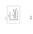
- FIG. 2A is an illustration of a PCB-based antenna array, in accordance with an embodiment of the invention.
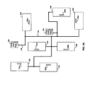
- FIG. 2B is a diagram of a 60 GHz inter-PCB communication system, in accordance with an embodiment of the invention.
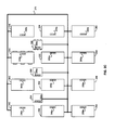
- FIG. 2C is a diagram of a 60 GHz inter-PCB communication system, in accordance with an embodiment of the invention.
- FIG. 3 is a flow chart illustrating an exemplary communication setup, in accordance with an embodiment of the invention.
- Certain embodiments of the invention may be found in a method and system for portable data storage with an integrated 60 GHz radio.
- Aspects of a method and system for portable data storage with an integrated 60 GHz radio may comprise setting up a microwave communication link between a first PCB and a second PCB via a wireline communication bus.
- the initialization may comprise adjusting beamforming parameters of a first antenna array communicatively coupled to the first PCB, and of a second antenna array communicatively coupled to the second PCB.
- the first PCB and the second PCB may communicate data via the microwave communication link.
- the microwave communication link may be routed via one or more relay PCBs, when the first PCB and the second PCB cannot directly communicate satisfactorily.
- Control data may be transferred between the first PCB, the second PCB, and/or the one or more relay PCBs, which may comprise one or more antennas.
- the relay PCBs may be dedicated relay PCBs or multi-purpose transmitter/receivers.
- the first PCB and the second PCB may receive and/or transmit signals in the 60 GHz frequency band.
- the first antenna array and/or the second antenna array may be on an integrated circuit package, or on an integrated circuit of the first PCB and/or the second PCB, respectively.
- the first antenna array and the second antenna array may comprise one or more antennas.
- the beamforming parameters may be adjusted to optimize a communication link performance metric.
- FIG. 1 is a diagram illustrating an exemplary wireless communication system, in accordance with an embodiment of the invention.
- an access point 112b there is shown an access point 112b, a computer 110a, a portable storage 114a, a router 130, the Internet 132 and a web server 134.
- the computer or host device 110a may comprise a wireless radio 111a, a short-range radio 111b, a host processor 111c, and a host memory 111d.
- a wireless connection between the wireless radio 111a and the access point 112b and a short-range wireless connection between the short-range radio 111 b and the portable storage 114a.
- the access point 112b may comprise suitable logic, circuitry and/or code that may be enabled to transmit and receive radio frequency signals for data communications, for example with the wireless radio 111a.
- the access point 112b may also be enabled to communicate via a wired network, for example, with the router 130.
- the wireless radio 111a may comprise suitable logic, circuitry and/or code that may enable communications over radio frequency waves with one or more other radio communication devices.
- the wireless radio 111a and the access point 112b may be compliant with one or more mobile communication standards, for example, GSM, UMTS, and/or CDMA2000.
- the short range radio 111 b may comprise suitable logic, circuitry and/or code that may enable communications over radio frequencies with one or more other communication devices, for example the portable storage 114a.
- the short range radio 111b and/or the portable storage 114a may be compliant with a wireless industry standard, for example Bluetooth, ZigBee, and/or IEEE 802.11 Wireless LAN.
- a plurality of PCBs similar to PCB 214 illustrated in FIG. 2A may communicate together at high data rates via, for example, 60 GHz wireless links via antenna arrays that may be implemented on and/or in the PCB as described above.
- one or more communication links may be established between, for example, PCB 214 and other PCBs associated to the device 202.
- the antenna array comprising antennas 206, 208, and 210, for example, may be enabled to automatically steer the transmission and/or reception beam in a direction that may optimize the signal quality and hence the data rates that may be achievable.
- FIG. 2B is a diagram of a 60 GHz inter-PCB communication system, in accordance with an embodiment of the invention. Referring to FIG. 2B , there is shown a wireline communication bus 238, PCBs 220, 222, 226, 228, 230, 234, and 236. There is also shown relay PCBs 224 and 232.
- Each of the PCBs 220, 222, 226, 228, 230, 234, and 236 may be substantially similar and may comprise suitable logic circuitry and/or code that may be enabled to communicate on one or more RF frequencies via corresponding antenna arrays.
- each of the PCBs 220, 222, 226, 228, 230, 234, and 236 may comprise an antenna array 220a, 222a, 226a, 228a, 230a, 234a, and 236a, respectively.
- the PCB 220 for example, may comprise suitable logic, circuitry and/or code that may be enabled to communicate on radio-frequency frequencies via the antenna array 220a, and via the wireline communication bus 238.
- the PCBs 220, 222, 226, 228, 230, 234, and 236 may be communicatively coupled to the wireline bus 238.
- relay PCBs 224 and 232 may be communicatively coupled to the wireline bus 238.
- relay PCBs for example relay PCBs 224 and 232, may be distinguished from other PCBs in that they may only forward data received via a radio link, and may not generally be the intended final recipients of data sent via a radio link. This may be, for example, the case for PCBs that may perform auxiliary functions that may not be directly involved in data processing, for example power supply PCBs.
- the wireline bus 238 may comprise suitable, logic, circuitry and/or code that may be enabled to carry communication signal that may be sent and received by entities communicatively coupled to the wireline bus 238.
- the wireline bus 238 may be used as a low rate communication bus and as a control signal transport media that may be utilized to establish a high-rate 60 GHz radio communication link between or among a plurality of PCBs.
- the PCB 220 and/or the PCB 226 may initiate a communication session and parameters for a wireless radio connection may be exchanged.
- the antenna array 220a on PCB 220 may be directed toward the antenna array 226a on PCB 226, and data may be exchanged wirelessly at a high-data rate.
- one or more PCBs may not be able to directly communicate with another PCB.
- the PCB220 may desire to communicate with the PCB 236.
- the PCB 236 may not be in line of sight of the PCB 220a because the PCB 226 and the relay PCB 232, may be obstructing a direct wireless link from PCB 220 to PCB 236.
- the communication may be routed via relay PCBs.
- the relay PCBs for example the PCBs 224 and 232 may be enabled to receive communication data from one PCB and forward it to another PCB.
- the PCB 220 may transmit to the PCB 236 via the relay PCB 224.
- the PCB 220 may communicate with the PCB 236 via the relay PCB 224 and the PCB 232.
- the PCB 222 may communicate with the PCB 234 via the relay PCB 232, for example.
- the wireline bus 238 may be utilized to exchange control information and/or wireless link setup information. High-rate transfer may be achieved via the antennas, for example antenna array 220a, which are PCB-based.
- FIG. 2C is a diagram of a 60 GHz inter-PCB communication system, in accordance with an embodiment of the invention. Referring to FIG. 2C , there is shown a wireline communication bus 270, PCBs 240, 242, 244, 246, 248, 250, 252, 254, 256, 258, 260 and 262. There is also shown relay PCBs 264, 266, and 268.
- the PCBs 240, 242, 244, 246, 248, 250, 252, 254, 256, 258, 260 and 262 may be substantially similar.
- each of the PCBs 240, 242, 244, 246, 248, 250, 252, 254, 256, 258, 260 and 262 may comprise an antenna array 240a, 242a, 244a, 246a, 248a, 250a, 252a, 254a, 256a, 258a, 260a and 262a, respectively.
- the PCBs 240, 242, 244, 246, 248, 250, 252, 254, 256, 258, 260 and 262 may be communicatively coupled to the wireline communication bus 270.
- the PCB 240 may comprise suitable logic, circuitry and/or code that may be enabled to communicate on radio-frequency frequencies via the antenna array 240a, and via the wireline communication bus 270.
- Each of the relay PCBs 264, 266, and 268 may be substantially similar to PCB 240.
- the relay PCBs 264, 266, and 268 may comprise one or more antenna arrays.
- the relay PCB 264 may comprise an antenna array 264a.
- the relay PCB 264 may comprise suitable logic, circuitry and/or code that may be enabled to communicate on radio-frequency frequencies via the antenna arrays 264a, and via wireline communication via the wireline communication bus 270.
- the relay PCBs 264, 266, and 268 may be communicatively coupled to the wireline communication bus 270.
- the wireline communication bus 270 may be used to exchange control information and setup a 60 GHz wireless connection between or among a plurality of PCBs.
- a regular grid of PCBs as illustrated in FIG. 2C may be utilized.
- various embodiments of the invention may comprise a high density of PCBs since fewer physical connections may be required.
- the PCB 256 may desire to communicate with the PCB 244.
- the communication parameters may be exchanged via the wireline communication bus 270, and a wireless communication may be initialized. In this instance, the PCB 256 may steer its antenna array 256a toward the relay PCB 264.
- the relay PCB 264 may relay messages from, and to the PCB 256 via the relay PCB 266 and/or the relay PCB 268.
- the relay PCBs may be dedicated relay PCBs and/or multi-purpose transmitter/receiver PCBs that may be enabled to initiate communication sessions on their own.
- dedicated relay PCBs for example relay PCBs 264. 266, and 268, may be distinguished from other PCBs in that they may only forward data received via a radio link, and may not generally be the intended final recipients of data sent via a radio link, for example a microwave link.
- multi-purpose transmitter/receiver PCBs for example PCBs 240, 242, or 244 may be enabled to relay received radio signal, but may also be the intended final recipient of signals that they may receive, for example via a microwave link.
- FIG. 3 is a flow chart illustrating an exemplary communication setup, in accordance with an embodiment of the invention.
- the communication setup process may be initialized in step 302.
- the initial communications setup may be established, for example between the PCB 250 and the PCB 254, as illustrated in FIG. 2C .
- the initialization of the communication may be achieved via a wireline bus, for example the wireline communication bus 270, as described with respect to at least FIG. 2B and FIG. 2C .
- the 60 GHz antenna arrays on the PCB for example PCB 250, may automatically and/or dynamically adjust their beam patterns in order to optimize some communication performance parameters.
- the beams may be adjusted in order to optimize signal strength, Signal-to-Interference-and-Noise-Ratio (SINR), packet error rate (PER) or bit error rate (BER).
- SINR Signal-to-Interference-and-Noise-Ratio
- PER packet error rate
- BER bit error rate
- the beam patterns and parameters may be adjusted, for example through transmitted and received training data.
- the transmission and reception of the data through the antenna arrays may take place.
- a plurality of communicating PCBs may be required to transmit and/or receive data via relay PCBs, for example relay PCBs 264, 266, and 268.
- a method and system for inter-PCB communications with wireline control may comprise setting up a microwave communication link between a first PCB, for example PCB 222, and a second PCB, for example 234, via a wireline communication bus 238.
- the initialization may comprise adjusting beamforming parameters of a first antenna array, for example 222a, communicatively coupled to the first PCB 222, and a second antenna array, for example 234a, communicatively coupled to the second PCB 234.
- the first PCB, for example PCB 222, and the second PCB, for example PCB 234, may communicate data via said microwave communication link, as described in FIG. 2B and FIG. 2C .
- the microwave communication link may be routed via one or more relay PCBs, for example relay PCB 232, when the first PCB, for example PCB 222, and the second PCB, for example PCB 234, cannot directly communicate.
- Control data may be transferred between the first PCB 222, the second PCB 234, and/or the one or more relay PCBs, for example relay PCB 232, which may comprise one or more antennas, for example antennas 232a and 232b.
- the relay PCBs may be dedicated relay PCBs or multi-purpose transmitter/receivers.
- the first PCB and the second PCB may receive and transmit in the 60 GHz frequency band.
- the first antenna array and/or the second antenna array may be on an integrated circuit package, or on an integrated circuit of the first PCB and/or the second PCB, respectively, as illustrated in FIG. 2A , for example.
- the first antenna array and the second antenna array may comprise one or more antennas.
- the beamforming parameters may be adjusted to optimize a microwave communication link performance metric.
- Another embodiment of the invention may provide a machine-readable storage, having stored thereon, a computer program having at least one code section executable by a machine, thereby causing the machine to perform the steps as described herein for a method and system for inter-PCB communications with wireline control.
- the present invention may be realized in hardware, software, or a combination of hardware and software.
- the present invention may be realized in a centralized fashion in at least one computer system, or in a distributed fashion where different elements are spread across several interconnected computer systems. Any kind of computer system or other apparatus adapted for carrying out the methods described herein is suited.
- a typical combination of hardware and software may be a general-purpose computer system with a computer program that, when being loaded and executed, controls the computer system such that it carries out the methods described herein.
Landscapes
- Engineering & Computer Science (AREA)
- Microelectronics & Electronic Packaging (AREA)
- Mobile Radio Communication Systems (AREA)
Abstract
Description
- Not applicable.
- Certain embodiments of the invention relate to communication systems. More specifically, certain embodiments of the invention relate to a method and system for inter-PCB communications with wireline control.
- Electronic communication has become prolific over the last decade. While electronic communication was initially limited to the desktop, recent trends have been to make communications, media content and the Internet available anytime, anywhere and, increasingly, on any device. Already now, it is quite common to find mobile devices such as cellular phones or Personal Digital Assistants (PDAs) that incorporate a large range of communication technologies and associated software. For example, fully-featured web-browsers, email clients, MP3 players, instant messenger software, and Voice-over-IP may all be found on some recent devices.
- Currently, there are many different communication technologies and protocols, some of which may utilize common data formats and while others may utilize different data formats. Today's mobile communication devices have to support these many different communication technologies, protocols and/or data formats.
- Further limitations and disadvantages of conventional and traditional approaches will become apparent to one of skill in the art, through comparison of such systems with some aspects of the present invention as set forth in the remainder of the present application with reference to the drawings.
- A method and/or system for PCB-to-PCB communications with wireline control, substantially as shown in and/or described in connection with at least one of the figures, as set forth more completely in the claims.
According to an aspect, a method for processing communication signals is provided, the method comprising: - setting up a microwave communication link between a first PCB and a second PCB via a wireline communication bus; and
- communicating data between said first PCB and said second PCB via said microwave communication link.
- one or more circuits in a first PCB and a second PCB communicatively coupled via a wireline communication bus, wherein said one or more circuits in said first PCB and/or said second PCB enable setup of a microwave communication link between said first PCB and said second PCB; and
- said one or more circuits in said first PCB and/or said second PCB enables communication of data between said first PCB and said second PCB via said microwave communication link.
- These and other advantages, aspects and novel features of the present invention, as well as details of an illustrated embodiment thereof, will be more fully understood from the following description and drawings.
-
FIG. 1 is a diagram illustrating an exemplary wireless communication system, in accordance with an embodiment of the invention. -
FIG. 2A is an illustration of a PCB-based antenna array, in accordance with an embodiment of the invention. -
FIG. 2B is a diagram of a 60 GHz inter-PCB communication system, in accordance with an embodiment of the invention. -
FIG. 2C is a diagram of a 60 GHz inter-PCB communication system, in accordance with an embodiment of the invention. -
FIG. 3 is a flow chart illustrating an exemplary communication setup, in accordance with an embodiment of the invention. - Certain embodiments of the invention may be found in a method and system for portable data storage with an integrated 60 GHz radio. Aspects of a method and system for portable data storage with an integrated 60 GHz radio may comprise setting up a microwave communication link between a first PCB and a second PCB via a wireline communication bus. The initialization may comprise adjusting beamforming parameters of a first antenna array communicatively coupled to the first PCB, and of a second antenna array communicatively coupled to the second PCB. The first PCB and the second PCB may communicate data via the microwave communication link.
- The microwave communication link may be routed via one or more relay PCBs, when the first PCB and the second PCB cannot directly communicate satisfactorily. Control data may be transferred between the first PCB, the second PCB, and/or the one or more relay PCBs, which may comprise one or more antennas. The relay PCBs may be dedicated relay PCBs or multi-purpose transmitter/receivers. The first PCB and the second PCB may receive and/or transmit signals in the 60 GHz frequency band. The first antenna array and/or the second antenna array may be on an integrated circuit package, or on an integrated circuit of the first PCB and/or the second PCB, respectively. The first antenna array and the second antenna array may comprise one or more antennas. The beamforming parameters may be adjusted to optimize a communication link performance metric.
-
FIG. 1 is a diagram illustrating an exemplary wireless communication system, in accordance with an embodiment of the invention. Referring toFIG. 1 , there is shown anaccess point 112b, acomputer 110a, aportable storage 114a, arouter 130, theInternet 132 and aweb server 134. The computer orhost device 110a may comprise awireless radio 111a, a short-range radio 111b, ahost processor 111c, and ahost memory 111d. There is also shown a wireless connection between thewireless radio 111a and theaccess point 112b, and a short-range wireless connection between the short-range radio 111 b and theportable storage 114a. - The
access point 112b may comprise suitable logic, circuitry and/or code that may be enabled to transmit and receive radio frequency signals for data communications, for example with thewireless radio 111a. Theaccess point 112b may also be enabled to communicate via a wired network, for example, with therouter 130. Thewireless radio 111a may comprise suitable logic, circuitry and/or code that may enable communications over radio frequency waves with one or more other radio communication devices. Thewireless radio 111a and theaccess point 112b may be compliant with one or more mobile communication standards, for example, GSM, UMTS, and/or CDMA2000. - The
short range radio 111 b may comprise suitable logic, circuitry and/or code that may enable communications over radio frequencies with one or more other communication devices, for example theportable storage 114a. Theshort range radio 111b and/or theportable storage 114a may be compliant with a wireless industry standard, for example Bluetooth, ZigBee, and/or IEEE 802.11 Wireless LAN. - The
host processor 111c may comprise suitable logic, circuitry and/or code that may be enabled to generate and process data. Thehost processor 111 c may be a general purpose processor suitable for acomputer 110a, or may be, for example, a PDA-like data processor for usage in a mobile communications computer or smartphone. - The
host memory 111 d may comprise suitable logic, circuitry and/or code that may be enabled to store and retrieve data for various system components and functions of thecomputer 110a. Thehost processor 111 c may be enabled to store information within thehost memory 111d and retrieved stored information from thehost memory 111d. - The
router 130 may comprise suitable logic, circuitry and/or code that may be enabled to communicate with various communication devices that may be communicatively coupled to it, for example, theaccess point 112b. Therouter 130 may be enabled to route communication between, for example, a wide area network (WAN) and/or a LAN or WLAN. Theaccess point 112b and theInternet 132 may be coupled to therouter 130. In this regard, therouter 132 may be enabled to route traffic between the Internet and devices communicatively coupled to a WLAN via theaccess point 112b. - The
Internet 132 may comprise various devices comprising suitable logic, circuitry and/or code that may enable interconnection and exchange of data between or among a plurality of communication devices communicatively coupled thereto. Theweb server 134 may comprise suitable logic, circuitry and/or code that may be communicatively coupled to theInternet 132 and may be enabled to provide web-based services to various communication devices that may be communicatively coupled to it. For example, theweb server 134 may host one or more web sites that may be accessible via the communication devices. - Frequently, computing and communication devices may comprise hardware and software that may enable communication using multiple wireless communication standards and/or protocols. There may be instances when the
wireless radio 111 a and the short-range radio 111b may be active concurrently. For example, it may be desirable for a user of the computer orhost device 110a to access theInternet 132 in order to consume streaming content from theWeb server 134. Accordingly, the user may establish a wireless connection between thecomputer 110a and theaccess point 112b. Once this connection is established, the streaming content from theWeb server 134 may be received via therouter 130, theaccess point 112b, and the wireless connection, and consumed by the computer orhost device 110a. - It may be desirable for the user of the
computer 110a to access data from theportable storage 114a. Accordingly, the user of thecomputer 110a may establish a short-range wireless connection with theportable storage 114a. In some instances, a wireless connection between theportable storage 114a and thecomputer 110a may be using a Bluetooth, ZigBee, WiMax, IEEE 802.11 Wireless LAN, Ultrawideband, or 60 GHz communications protocol. When the short-range wireless connection is established, and with suitable configurations on thecomputer 110a enabled, data may be transferred from/to theportable storage 114a. In some instances, the data link between theportable storage 114a and thecomputer 110a may be enabled for high data rates. To achieve high data rates in compact devices, for example theportable storage 114a, wireless communication links to connect the components of a device. For example, the Printed Circuit Boards (PCBs) within theportable storage 114a may communicate data at high rate, for example in the Gbps range, via wireless links, for example via a 60 GHz microwave link. -
FIG. 2A is an illustration of a PCB-based antenna array, in accordance with an embodiment of the invention. Referring toFIG. 2A , there is shown adevice 202. Thedevice 202 may comprise acasing 204, and one or more printed circuit boards (PCBs) 214. ThePCB 214 may comprise one or more antennas, of whichantennas device 202 may be, for example, a portable storage device. - The
PCB 214 may comprise suitable logic, circuitry and/or code that may be enabled to generate and/or process radio frequency signals for reception and/or transmission via the one or more antennas, of whichantennas antennas antennas PCB 214. - In accordance with various embodiments of the invention, a plurality of PCBs similar to
PCB 214 illustrated inFIG. 2A may communicate together at high data rates via, for example, 60 GHz wireless links via antenna arrays that may be implemented on and/or in the PCB as described above. - In accordance with an embodiment of the invention, one or more communication links may be established between, for example,
PCB 214 and other PCBs associated to thedevice 202. In addition, the antennaarray comprising antennas -
FIG. 2B is a diagram of a 60 GHz inter-PCB communication system, in accordance with an embodiment of the invention. Referring toFIG. 2B , there is shown awireline communication bus 238,PCBs relay PCBs - Each of the
PCBs PCBs antenna array PCB 220, for example, may comprise suitable logic, circuitry and/or code that may be enabled to communicate on radio-frequency frequencies via theantenna array 220a, and via thewireline communication bus 238. ThePCBs wireline bus 238. - Each of the
relay PCBs PCBs PCB 224 may comprise anantenna array 224a and anantenna array 224b. Similarly, therelay PCB 232 may compriseantenna arrays relay PCB 232, for example, may comprise suitable logic, circuitry and/or code that may be enabled to communicate on radio-frequency frequencies via theantenna arrays wireline communication bus 238. Therelay PCBs wireline bus 238. In some instances, relay PCBs, forexample relay PCBs - The
wireline bus 238 may comprise suitable, logic, circuitry and/or code that may be enabled to carry communication signal that may be sent and received by entities communicatively coupled to thewireline bus 238. Thewireline bus 238 may be used as a low rate communication bus and as a control signal transport media that may be utilized to establish a high-rate 60 GHz radio communication link between or among a plurality of PCBs. For example, it may be desirable for thePCB 220 to communicate with thePCB 226. Via thewireline bus 238, thePCB 220 and/or thePCB 226 may initiate a communication session and parameters for a wireless radio connection may be exchanged. When the setup phase may be completed, theantenna array 220a onPCB 220 may be directed toward theantenna array 226a onPCB 226, and data may be exchanged wirelessly at a high-data rate. In some instances, one or more PCBs may not be able to directly communicate with another PCB. For example, the PCB220 may desire to communicate with thePCB 236. - As illustrated in
FIG. 2B , in some instances, thePCB 236 may not be in line of sight of thePCB 220a because thePCB 226 and therelay PCB 232, may be obstructing a direct wireless link fromPCB 220 toPCB 236. In these instances, the communication may be routed via relay PCBs. The relay PCBs, for example thePCBs PCB 220 may transmit to thePCB 236 via therelay PCB 224. In another embodiment of the invention, thePCB 220 may communicate with thePCB 236 via therelay PCB 224 and thePCB 232. Similarly, thePCB 222 may communicate with thePCB 234 via therelay PCB 232, for example. In accordance with various embodiments of the invention, thewireline bus 238 may be utilized to exchange control information and/or wireless link setup information. High-rate transfer may be achieved via the antennas, forexample antenna array 220a, which are PCB-based. -
FIG. 2C is a diagram of a 60 GHz inter-PCB communication system, in accordance with an embodiment of the invention. Referring toFIG. 2C , there is shown awireline communication bus 270,PCBs relay PCBs - The
PCBs PCBs antenna array PCBs wireline communication bus 270. - The
PCB 240, for example, may comprise suitable logic, circuitry and/or code that may be enabled to communicate on radio-frequency frequencies via theantenna array 240a, and via thewireline communication bus 270. - Each of the
relay PCBs PCB 240. Therelay PCBs relay PCB 264 may comprise anantenna array 264a. Therelay PCB 264, for example, may comprise suitable logic, circuitry and/or code that may be enabled to communicate on radio-frequency frequencies via theantenna arrays 264a, and via wireline communication via thewireline communication bus 270. Therelay PCBs wireline communication bus 270. - Similar to
FIG. 2B , thewireline communication bus 270 may be used to exchange control information and setup a 60 GHz wireless connection between or among a plurality of PCBs. In some instances, a regular grid of PCBs as illustrated inFIG. 2C may be utilized. As illustrated, because of the wireless links, various embodiments of the invention may comprise a high density of PCBs since fewer physical connections may be required. For example, thePCB 256 may desire to communicate with thePCB 244. The communication parameters may be exchanged via thewireline communication bus 270, and a wireless communication may be initialized. In this instance, thePCB 256 may steer itsantenna array 256a toward therelay PCB 264. Therelay PCB 264 may relay messages from, and to thePCB 256 via therelay PCB 266 and/or therelay PCB 268. In accordance with various embodiments of the invention, the relay PCBs may be dedicated relay PCBs and/or multi-purpose transmitter/receiver PCBs that may be enabled to initiate communication sessions on their own. As described above forFIG. 2A , dedicated relay PCBs, forexample relay PCBs 264. 266, and 268, may be distinguished from other PCBs in that they may only forward data received via a radio link, and may not generally be the intended final recipients of data sent via a radio link, for example a microwave link. This may be, for example, the case for PCBs that may perform auxiliary functions that may not be directly involved in data processing, for example power supply PCBs. Conversely, multi-purpose transmitter/receiver PCBs, forexample PCBs -
FIG. 3 is a flow chart illustrating an exemplary communication setup, in accordance with an embodiment of the invention. The communication setup process may be initialized instep 302. Instep 304, the initial communications setup may be established, for example between thePCB 250 and thePCB 254, as illustrated inFIG. 2C . In accordance with various embodiments of the invention, the initialization of the communication may be achieved via a wireline bus, for example thewireline communication bus 270, as described with respect to at leastFIG. 2B andFIG. 2C . Instep 306, after the connection has been set up, the 60 GHz antenna arrays on the PCB, forexample PCB 250, may automatically and/or dynamically adjust their beam patterns in order to optimize some communication performance parameters. For example, the beams may be adjusted in order to optimize signal strength, Signal-to-Interference-and-Noise-Ratio (SINR), packet error rate (PER) or bit error rate (BER). The beam patterns and parameters may be adjusted, for example through transmitted and received training data. Instep 308, the transmission and reception of the data through the antenna arrays may take place. In some instances, a plurality of communicating PCBs may be required to transmit and/or receive data via relay PCBs, forexample relay PCBs - In accordance with an embodiment of the invention, a method and system for inter-PCB communications with wireline control may comprise setting up a microwave communication link between a first PCB, for
example PCB 222, and a second PCB, for example 234, via awireline communication bus 238. The initialization may comprise adjusting beamforming parameters of a first antenna array, for example 222a, communicatively coupled to thefirst PCB 222, and a second antenna array, for example 234a, communicatively coupled to thesecond PCB 234. The first PCB, forexample PCB 222, and the second PCB, forexample PCB 234, may communicate data via said microwave communication link, as described inFIG. 2B andFIG. 2C . The microwave communication link may be routed via one or more relay PCBs, forexample relay PCB 232, when the first PCB, forexample PCB 222, and the second PCB, forexample PCB 234, cannot directly communicate. Control data may be transferred between thefirst PCB 222, thesecond PCB 234, and/or the one or more relay PCBs, forexample relay PCB 232, which may comprise one or more antennas, forexample antennas FIG. 2A , for example. The first antenna array and the second antenna array may comprise one or more antennas. The beamforming parameters may be adjusted to optimize a microwave communication link performance metric. - Another embodiment of the invention may provide a machine-readable storage, having stored thereon, a computer program having at least one code section executable by a machine, thereby causing the machine to perform the steps as described herein for a method and system for inter-PCB communications with wireline control.
- Accordingly, the present invention may be realized in hardware, software, or a combination of hardware and software. The present invention may be realized in a centralized fashion in at least one computer system, or in a distributed fashion where different elements are spread across several interconnected computer systems. Any kind of computer system or other apparatus adapted for carrying out the methods described herein is suited. A typical combination of hardware and software may be a general-purpose computer system with a computer program that, when being loaded and executed, controls the computer system such that it carries out the methods described herein.
- The present invention may also be embedded in a computer program product, which comprises all the features enabling the implementation of the methods described herein, and which when loaded in a computer system is able to carry out these methods. Computer program in the present context means any expression, in any language, code or notation, of a set of instructions intended to cause a system having an information processing capability to perform a particular function either directly or after either or both of the following: a) conversion to another language, code or notation; b) reproduction in a different material form.
- While the present invention has been described with reference to certain embodiments, it will be understood by those skilled in the art that various changes may be made and equivalents may be substituted without departing from the scope of the present invention. In addition, many modifications may be made to adapt a particular situation or material to the teachings of the present invention without departing from its scope. Therefore, it is intended that the present invention not be limited to the particular embodiment disclosed, but that the present invention will include all embodiments falling within the scope of the appended claims.
Advantageously, the method further comprises transferring control data between said first PCB, said second PCB, and/or said one or more relay PCBs.
Advantageously, said one or more relay PCBs comprise one or more antennas.
Advantageously, said relay PCBs are dedicated relay PCBs.
Advantageously, said relay PCBs are multi-purpose transmitter/receivers.
Advantageously, said first PCB and said second PCB receive and transmit in the 60 GHz frequency band.
Advantageously, the method further comprises adjusting beamforming parameters of a first antenna array communicatively coupled to said first PCB, and of a second antenna array communicatively coupled to said second PCB.
Advantageously, said first antenna array is on an integrated circuit package, or on an integrated circuit of said first PCB.
Advantageously, said second antenna array is on an integrated circuit package, or on an integrated circuit of said second PCB.
Advantageously, said first antenna array and said second antenna array comprise one or more antennas.
Advantageously, the method further comprises adjusting said beamforming parameters to optimize a microwave communication link performance metric.
According to an aspect, a system for processing communication signals comprises:
Advantageously, said one or more circuits in said first PCB and/or said second PCB transfer control data between said first PCB, said second PCB, and/or said one or more relay PCBs.
Advantageously, said one or more relay PCBs comprise one or more antennas.
Advantageously, said relay PCBs are dedicated relay PCBs.
Advantageously, said relay PCBs are multi-purpose transmitter/receivers.
Advantageously, said first PCB and said second PCB receive and transmit in the 60 GHz frequency band.
Advantageously, said one or more circuits in said first PCB and/or said second PCB enables of adjustment of beamforming parameters of a first antenna array communicatively coupled to said first PCB, and of a second antenna array communicatively coupled to said second PCB.
Advantageously, said first antenna array is on an integrated circuit package, or on an integrated circuit of said first PCB.
Advantageously, said second antenna array is on an integrated circuit package, or on an integrated circuit of said second PCB.
Advantageously, said first antenna array and said second antenna array comprise one or more antennas.
Advantageously, said one or more circuits in said first PCB and/or said second PCB enables adjustment of said beamforming parameters to optimize a microwave communication link performance metric.
Claims (10)
- A method for processing communication signals, the method comprising:setting up a microwave communication link between a first PCB and a second PCB via a wireline communication bus; andcommunicating data between said first PCB and said second PCB via said microwave communication link.
- The method according to claim 1, comprising routing said microwave communication link via one or more relay PCBs, when said first PCB and said second PCB cannot directly communicate.
- The method according to claim 2, comprising transferring control data between said first PCB, said second PCB, and/or said one or more relay PCBs.
- The method according to claim 2, wherein said one or more relay PCBs comprise one or more antennas.
- The method according to claim 2, wherein said relay PCBs are dedicated relay PCBs.
- The method according to claim 2, wherein said relay PCBs are multi-purpose transmitter/receivers.
- A system for processing communication signals, the system comprising:one or more circuits in a first PCB and a second PCB communicatively coupled via a wireline communication bus, wherein said one or more circuits in said first PCB and/or said second PCB enable setup of a microwave communication link between said first PCB and said second PCB; andsaid one or more circuits in said first PCB and/or said second PCB enables communication of data between said first PCB and said second PCB via said microwave communication link.
- The system according to claim 7, wherein said one or more circuits in said first PCB and/or said second PCB route said microwave communication link via one or more relay PCBs, when said first PCB and said second PCB cannot directly communicate.
- The system according to claim 8, wherein said one or more circuits in said first PCB and/or said second PCB transfer control data between said first PCB, said second PCB, and/or said one or more relay PCBs.
- The system according to claim 8, wherein said one or more relay PCBs comprise one or more antennas.
Applications Claiming Priority (1)
| Application Number | Priority Date | Filing Date | Title |
|---|---|---|---|
| US12/056,865 US8144674B2 (en) | 2008-03-27 | 2008-03-27 | Method and system for inter-PCB communications with wireline control |
Publications (3)
| Publication Number | Publication Date |
|---|---|
| EP2106176A2 true EP2106176A2 (en) | 2009-09-30 |
| EP2106176A3 EP2106176A3 (en) | 2013-10-30 |
| EP2106176B1 EP2106176B1 (en) | 2016-05-11 |
Family
ID=40651987
Family Applications (1)
| Application Number | Title | Priority Date | Filing Date |
|---|---|---|---|
| EP09004055.1A Ceased EP2106176B1 (en) | 2008-03-27 | 2009-03-20 | Method and system for inter-PCB communications with wireline control |
Country Status (2)
| Country | Link |
|---|---|
| US (2) | US8144674B2 (en) |
| EP (1) | EP2106176B1 (en) |
Families Citing this family (12)
| Publication number | Priority date | Publication date | Assignee | Title |
|---|---|---|---|---|
| US8284822B2 (en) * | 2007-02-27 | 2012-10-09 | Broadcom Corporation | Method and system for utilizing direct digital frequency synthesis to process signals in multi-band applications |
| US7826550B2 (en) * | 2007-02-28 | 2010-11-02 | Broadcom Corp. | Method and system for a high-precision frequency generator using a direct digital frequency synthesizer for transmitters and receivers |
| US20080205545A1 (en) * | 2007-02-28 | 2008-08-28 | Ahmadreza Rofougaran | Method and System for Using a Phase Locked Loop for Upconversion in a Wideband Crystalless Polar Transmitter |
| US20080205550A1 (en) * | 2007-02-28 | 2008-08-28 | Ahmadreza Rofougaran | Method and System for Using a Phase Locked Loop for Upconversion in a Wideband Polar Transmitter |
| US8116387B2 (en) * | 2007-03-01 | 2012-02-14 | Broadcom Corporation | Method and system for a digital polar transmitter |
| US8494030B2 (en) * | 2008-06-19 | 2013-07-23 | Broadcom Corporation | Method and system for 60 GHz wireless clock distribution |
| US8483623B2 (en) * | 2008-06-19 | 2013-07-09 | Broadcom Corporation | Method and system for frequency-shift based PCB-to-PCB communications |
| US8429320B2 (en) * | 2009-12-18 | 2013-04-23 | Broadcom Corporation | Method and system for dynamically programmable serial/parallel bus interface |
| US9794522B2 (en) * | 2015-02-06 | 2017-10-17 | Google Inc. | Systems, methods, and devices for managing coexistence of multiple transceiver devices by optimizing component layout |
| US10687184B2 (en) | 2016-05-13 | 2020-06-16 | Google Llc | Systems, methods, and devices for utilizing radar-based touch interfaces |
| US11152664B2 (en) * | 2019-12-24 | 2021-10-19 | Anexa Labs Llc | Compact electronics with optical sensors |
| US11156965B1 (en) | 2020-10-23 | 2021-10-26 | Anexa Labs Llc | Latching mechanism for securing two objects |
Family Cites Families (64)
| Publication number | Priority date | Publication date | Assignee | Title |
|---|---|---|---|---|
| JPH0319358A (en) | 1989-06-16 | 1991-01-28 | Matsushita Electron Corp | Semiconductor integrated circuit |
| US5015972A (en) | 1989-08-17 | 1991-05-14 | Motorola, Inc. | Broadband RF transformer |
| US5003622A (en) | 1989-09-26 | 1991-03-26 | Astec International Limited | Printed circuit transformer |
| AU4896396A (en) | 1995-01-06 | 1996-07-24 | Georgia Tech Research Corporation | Curtain antenna |
| US5861853A (en) | 1997-05-07 | 1999-01-19 | Motorola, Inc. | Current balanced balun network with selectable port impedances |
| US5914873A (en) | 1997-06-30 | 1999-06-22 | Advanced Micro Devices | Distributed voltage converter apparatus and method for high power microprocessor with array connections |
| US5798567A (en) | 1997-08-21 | 1998-08-25 | Hewlett-Packard Company | Ball grid array integrated circuit package which employs a flip chip integrated circuit and decoupling capacitors |
| US6060433A (en) | 1998-01-26 | 2000-05-09 | Nz Applied Technologies Corporation | Method of making a microwave device having a polycrystalline ferrite substrate |
| JP2000196329A (en) | 1998-12-24 | 2000-07-14 | Nec Corp | Phased array antenna and method of manufacturing the same |
| US6573808B1 (en) | 1999-03-12 | 2003-06-03 | Harris Broadband Wireless Access, Inc. | Millimeter wave front end |
| AU2001249797A1 (en) | 2000-04-04 | 2001-10-15 | Contact Technology Systems, Inc. | Arc fault current interrupter testing device |
| US6856225B1 (en) | 2000-05-17 | 2005-02-15 | Xerox Corporation | Photolithographically-patterned out-of-plane coil structures and method of making |
| US7247932B1 (en) | 2000-05-19 | 2007-07-24 | Megica Corporation | Chip package with capacitor |
| US7710199B2 (en) | 2000-09-12 | 2010-05-04 | Black Sand Technologies, Inc. | Method and apparatus for stabilizing RF power amplifiers |
| AU2002317857A1 (en) * | 2001-06-29 | 2003-03-03 | Vivactiss Bvba | Intelligent microplates with remote data access |
| JP4135861B2 (en) | 2001-10-03 | 2008-08-20 | 日本電波工業株式会社 | Multi-element planar antenna |
| JP3664721B2 (en) | 2001-12-04 | 2005-06-29 | 松下電器産業株式会社 | Antenna and device equipped with the antenna |
| US6801114B2 (en) | 2002-01-23 | 2004-10-05 | Broadcom Corp. | Integrated radio having on-chip transformer balun |
| US6646581B1 (en) | 2002-02-28 | 2003-11-11 | Silicon Laboratories, Inc. | Digital-to-analog converter circuit incorporating hybrid sigma-delta modulator circuit |
| US6809581B2 (en) | 2002-04-23 | 2004-10-26 | Broadcom Corp. | Integrated circuit low noise amplifier and applications thereof |
| US7260424B2 (en) | 2002-05-24 | 2007-08-21 | Schmidt Dominik J | Dynamically configured antenna for multiple frequencies and bandwidths |
| JP2003347844A (en) | 2002-05-29 | 2003-12-05 | Fujitsu Ltd | Voltage controlled oscillator, PLL circuit and semiconductor device |
| US20040010554A1 (en) * | 2002-07-15 | 2004-01-15 | Hall John M. | Determining a destination e-mail address for sending scanned documents |
| US7138884B2 (en) | 2002-08-19 | 2006-11-21 | Dsp Group Inc. | Circuit package integrating passive radio frequency structure |
| US6590543B1 (en) * | 2002-10-04 | 2003-07-08 | Bae Systems Information And Electronic Systems Integration Inc | Double monopole meanderline loaded antenna |
| US7141883B2 (en) | 2002-10-15 | 2006-11-28 | Silicon Laboratories Inc. | Integrated circuit package configuration incorporating shielded circuit element structure |
| US7532605B2 (en) * | 2003-01-07 | 2009-05-12 | Hewlett-Packard Development Company, L.P. | MAC-PHY interfacing for wireless devices |
| KR100498484B1 (en) | 2003-01-30 | 2005-07-01 | 삼성전자주식회사 | Wide band voltage controlled oscillator with constant gain and method thereof |
| US6975267B2 (en) | 2003-02-05 | 2005-12-13 | Northrop Grumman Corporation | Low profile active electronically scanned antenna (AESA) for Ka-band radar systems |
| US7151506B2 (en) | 2003-04-11 | 2006-12-19 | Qortek, Inc. | Electromagnetic energy coupling mechanism with matrix architecture control |
| DE10336171B3 (en) | 2003-08-07 | 2005-02-10 | Technische Universität Braunschweig Carolo-Wilhelmina | Multi-chip circuit module and method of making this |
| US6933789B2 (en) | 2003-11-13 | 2005-08-23 | Skyworks Solutions, Inc. | On-chip VCO calibration |
| JP4335661B2 (en) | 2003-12-24 | 2009-09-30 | Necエレクトロニクス株式会社 | Manufacturing method of high frequency module |
| US7196607B2 (en) | 2004-03-26 | 2007-03-27 | Harris Corporation | Embedded toroidal transformers in ceramic substrates |
| US7119745B2 (en) | 2004-06-30 | 2006-10-10 | International Business Machines Corporation | Apparatus and method for constructing and packaging printed antenna devices |
| US7081800B2 (en) | 2004-06-30 | 2006-07-25 | Intel Corporation | Package integrated one-quarter wavelength and three-quarter wavelength balun |
| US7053847B2 (en) | 2004-08-11 | 2006-05-30 | Northrop Grumman Corporation | Millimeter wave phased array systems with ring slot radiator element |
| US8463946B2 (en) * | 2004-09-17 | 2013-06-11 | Caterpillar Inc. | Method for automatic radio operational mode selection |
| WO2006039699A2 (en) | 2004-10-01 | 2006-04-13 | De Rochemont L Pierre | Ceramic antenna module and methods of manufacture thereof |
| US7129784B2 (en) | 2004-10-28 | 2006-10-31 | Broadcom Corporation | Multilevel power amplifier architecture using multi-tap transformer |
| US7469152B2 (en) | 2004-11-30 | 2008-12-23 | The Regents Of The University Of California | Method and apparatus for an adaptive multiple-input multiple-output (MIMO) wireless communications systems |
| US7307341B2 (en) | 2005-01-10 | 2007-12-11 | Ixys Corporation | Integrated packaged having magnetic components |
| US7038625B1 (en) | 2005-01-14 | 2006-05-02 | Harris Corporation | Array antenna including a monolithic antenna feed assembly and related methods |
| US20060211449A1 (en) * | 2005-03-18 | 2006-09-21 | Honeywell International Inc. | Reconfigurable wireless interconnects for data communication |
| CA2503306A1 (en) * | 2005-03-30 | 2006-09-30 | Paul J. Harvey | System and method for intra-cabinet wireless communication |
| US7834808B2 (en) | 2005-06-29 | 2010-11-16 | Georgia Tech Research Corporation | Multilayer electronic component systems and methods of manufacture |
| US7579589B2 (en) | 2005-07-26 | 2009-08-25 | Sionex Corporation | Ultra compact ion mobility based analyzer apparatus, method, and system |
| MX2008010112A (en) | 2006-02-09 | 2009-03-05 | Card Logistics Properties Ltd | Proximity locator system. |
| JP2007234896A (en) | 2006-03-01 | 2007-09-13 | Toyota Motor Corp | Signal transmission device |
| US7558484B2 (en) * | 2006-03-06 | 2009-07-07 | Chang Gung Memorial University | Ultra-wide band wireless system |
| KR100853670B1 (en) | 2006-04-03 | 2008-08-25 | (주)에이스안테나 | Dual polarized broadband antenna with single pattern |
| DE102006035204B4 (en) | 2006-07-29 | 2009-10-15 | Atmel Duisburg Gmbh | Monolithically integrated circuit arrangement |
| US20080181185A1 (en) * | 2007-01-30 | 2008-07-31 | Broadcom Corporation | Dynamic multi-patch based frequency division multiple access frequency assignment |
| US7899407B2 (en) * | 2007-05-01 | 2011-03-01 | Broadcom Corporation | High frequency signal combining |
| US7675465B2 (en) | 2007-05-22 | 2010-03-09 | Sibeam, Inc. | Surface mountable integrated circuit packaging scheme |
| US8005437B2 (en) * | 2007-06-14 | 2011-08-23 | Broadcom Corporation | Fully integrated micro-strip VCO |
| WO2009002464A2 (en) * | 2007-06-22 | 2008-12-31 | Vubiq Incorporated | System and method for wireless communication in a backplane fabric architecture |
| US8270912B2 (en) | 2007-12-12 | 2012-09-18 | Broadcom Corporation | Method and system for a transformer in an integrated circuit package |
| US8855093B2 (en) * | 2007-12-12 | 2014-10-07 | Broadcom Corporation | Method and system for chip-to-chip communications with wireline control |
| US7911388B2 (en) | 2007-12-12 | 2011-03-22 | Broadcom Corporation | Method and system for configurable antenna in an integrated circuit package |
| US20090153260A1 (en) | 2007-12-12 | 2009-06-18 | Ahmadreza Rofougaran | Method and system for a configurable transformer integrated on chip |
| US20090243741A1 (en) | 2008-03-27 | 2009-10-01 | Ahmadreza Rofougaran | Method and system for processing signals via an oscillator load embedded in an integrated circuit (ic) package |
| US8072287B2 (en) | 2008-03-27 | 2011-12-06 | Broadcom Corporation | Method and system for configurable differential or single-ended signaling in an integrated circuit |
| US8198714B2 (en) | 2008-03-28 | 2012-06-12 | Broadcom Corporation | Method and system for configuring a transformer embedded in a multi-layer integrated circuit (IC) package |
-
2008
- 2008-03-27 US US12/056,865 patent/US8144674B2/en not_active Expired - Fee Related
-
2009
- 2009-03-20 EP EP09004055.1A patent/EP2106176B1/en not_active Ceased
-
2012
- 2012-02-24 US US13/405,048 patent/US8582546B2/en not_active Expired - Fee Related
Also Published As
| Publication number | Publication date |
|---|---|
| US8582546B2 (en) | 2013-11-12 |
| US20120159023A1 (en) | 2012-06-21 |
| US20090248929A1 (en) | 2009-10-01 |
| EP2106176B1 (en) | 2016-05-11 |
| US8144674B2 (en) | 2012-03-27 |
| EP2106176A3 (en) | 2013-10-30 |
Similar Documents
| Publication | Publication Date | Title |
|---|---|---|
| EP2106176B1 (en) | Method and system for inter-PCB communications with wireline control | |
| CN101459442B (en) | Method and system for processing communication signal | |
| EP2071471B1 (en) | Method and system for chip-to-chip communications with wireline control | |
| US8023992B2 (en) | Mobile wireless communications device providing pattern/frequency control features and related methods | |
| US8588279B2 (en) | Method and system for inter-PCB communication utilizing a spatial multi-link repeater | |
| US8583046B2 (en) | Method and system for portable data storage with integrated 60 GHz radio | |
| JP2020523940A (en) | Measurement setting method, terminal and base station | |
| CN101926096A (en) | Integrated antenna array and RF front end module | |
| US8090313B2 (en) | Method and system for frequency-shift based chip-to-chip communications | |
| US9391765B2 (en) | Wireless clock distribution | |
| US8483623B2 (en) | Method and system for frequency-shift based PCB-to-PCB communications | |
| US8064936B2 (en) | Method and system for a multistandard proxy | |
| CN111757351B (en) | Data receiving and sending method and device | |
| CN113098576B (en) | Data transceiver method, device and electronic device | |
| HK1138122B (en) | A method for processing communication signal and a system for processing communication signal | |
| US9591695B2 (en) | Method and system for sharing modulation information between multiple access points | |
| US8914062B2 (en) | Dual communications network base station apparatus | |
| CN116545550A (en) | Configuration information generation method and device, network equipment and storage medium | |
| HK1138123B (en) | A method and system for processing communication signal |
Legal Events
| Date | Code | Title | Description |
|---|---|---|---|
| PUAI | Public reference made under article 153(3) epc to a published international application that has entered the european phase |
Free format text: ORIGINAL CODE: 0009012 |
|
| 17P | Request for examination filed |
Effective date: 20090320 |
|
| AK | Designated contracting states |
Kind code of ref document: A2 Designated state(s): AT BE BG CH CY CZ DE DK EE ES FI FR GB GR HR HU IE IS IT LI LT LU LV MC MK MT NL NO PL PT RO SE SI SK TR |
|
| AX | Request for extension of the european patent |
Extension state: AL BA RS |
|
| REG | Reference to a national code |
Ref country code: DE Ref legal event code: R079 Ref document number: 602009038542 Country of ref document: DE Free format text: PREVIOUS MAIN CLASS: H04W0024020000 Ipc: G06F0015163000 |
|
| PUAL | Search report despatched |
Free format text: ORIGINAL CODE: 0009013 |
|
| AK | Designated contracting states |
Kind code of ref document: A3 Designated state(s): AT BE BG CH CY CZ DE DK EE ES FI FR GB GR HR HU IE IS IT LI LT LU LV MC MK MT NL NO PL PT RO SE SI SK TR |
|
| AX | Request for extension of the european patent |
Extension state: AL BA RS |
|
| RIC1 | Information provided on ipc code assigned before grant |
Ipc: G06F 15/163 20060101AFI20130924BHEP |
|
| 17Q | First examination report despatched |
Effective date: 20131025 |
|
| RBV | Designated contracting states (corrected) |
Designated state(s): AT BE BG CH CY CZ DE DK EE ES FI FR GB GR HR HU IE IS IT LI LT LU LV MC MK MT NL NO PL PT RO SE SI SK TR |
|
| AKX | Designation fees paid |
Designated state(s): DE GB |
|
| GRAP | Despatch of communication of intention to grant a patent |
Free format text: ORIGINAL CODE: EPIDOSNIGR1 |
|
| INTG | Intention to grant announced |
Effective date: 20151027 |
|
| GRAS | Grant fee paid |
Free format text: ORIGINAL CODE: EPIDOSNIGR3 |
|
| GRAA | (expected) grant |
Free format text: ORIGINAL CODE: 0009210 |
|
| AK | Designated contracting states |
Kind code of ref document: B1 Designated state(s): DE GB |
|
| REG | Reference to a national code |
Ref country code: GB Ref legal event code: FG4D |
|
| REG | Reference to a national code |
Ref country code: DE Ref legal event code: R096 Ref document number: 602009038542 Country of ref document: DE |
|
| REG | Reference to a national code |
Ref country code: DE Ref legal event code: R097 Ref document number: 602009038542 Country of ref document: DE |
|
| REG | Reference to a national code |
Ref country code: DE Ref legal event code: R082 Ref document number: 602009038542 Country of ref document: DE Representative=s name: BOSCH JEHLE PATENTANWALTSGESELLSCHAFT MBH, DE Ref country code: DE Ref legal event code: R081 Ref document number: 602009038542 Country of ref document: DE Owner name: AVAGO TECHNOLOGIES INTERNATIONAL SALES PTE. LT, SG Free format text: FORMER OWNER: BROADCOM CORPORATION, IRVINE, CALIF., US Ref country code: DE Ref legal event code: R081 Ref document number: 602009038542 Country of ref document: DE Owner name: AVAGO TECHNOLOGIES GENERAL IP (SINGAPORE) PTE., SG Free format text: FORMER OWNER: BROADCOM CORPORATION, IRVINE, CALIF., US |
|
| PLBE | No opposition filed within time limit |
Free format text: ORIGINAL CODE: 0009261 |
|
| STAA | Information on the status of an ep patent application or granted ep patent |
Free format text: STATUS: NO OPPOSITION FILED WITHIN TIME LIMIT |
|
| 26N | No opposition filed |
Effective date: 20170214 |
|
| GBPC | Gb: european patent ceased through non-payment of renewal fee |
Effective date: 20170320 |
|
| PG25 | Lapsed in a contracting state [announced via postgrant information from national office to epo] |
Ref country code: GB Free format text: LAPSE BECAUSE OF NON-PAYMENT OF DUE FEES Effective date: 20170320 |
|
| REG | Reference to a national code |
Ref country code: DE Ref legal event code: R082 Ref document number: 602009038542 Country of ref document: DE Representative=s name: BOSCH JEHLE PATENTANWALTSGESELLSCHAFT MBH, DE Ref country code: DE Ref legal event code: R081 Ref document number: 602009038542 Country of ref document: DE Owner name: AVAGO TECHNOLOGIES INTERNATIONAL SALES PTE. LT, SG Free format text: FORMER OWNER: AVAGO TECHNOLOGIES GENERAL IP (SINGAPORE) PTE. LTD., SINGAPORE, SG |
|
| PGFP | Annual fee paid to national office [announced via postgrant information from national office to epo] |
Ref country code: DE Payment date: 20220310 Year of fee payment: 14 |
|
| REG | Reference to a national code |
Ref country code: DE Ref legal event code: R119 Ref document number: 602009038542 Country of ref document: DE |
|
| PG25 | Lapsed in a contracting state [announced via postgrant information from national office to epo] |
Ref country code: DE Free format text: LAPSE BECAUSE OF NON-PAYMENT OF DUE FEES Effective date: 20231003 |