EP2096683B1 - Method for fabricating a semiconductor substrate - Google Patents
Method for fabricating a semiconductor substrate Download PDFInfo
- Publication number
- EP2096683B1 EP2096683B1 EP08290176A EP08290176A EP2096683B1 EP 2096683 B1 EP2096683 B1 EP 2096683B1 EP 08290176 A EP08290176 A EP 08290176A EP 08290176 A EP08290176 A EP 08290176A EP 2096683 B1 EP2096683 B1 EP 2096683B1
- Authority
- EP
- European Patent Office
- Prior art keywords
- semiconductor layer
- substrate
- layer
- modified
- donor
- Prior art date
- Legal status (The legal status is an assumption and is not a legal conclusion. Google has not performed a legal analysis and makes no representation as to the accuracy of the status listed.)
- Active
Links
Images

Classifications
-
- H—ELECTRICITY
- H10—SEMICONDUCTOR DEVICES; ELECTRIC SOLID-STATE DEVICES NOT OTHERWISE PROVIDED FOR
- H10F—INORGANIC SEMICONDUCTOR DEVICES SENSITIVE TO INFRARED RADIATION, LIGHT, ELECTROMAGNETIC RADIATION OF SHORTER WAVELENGTH OR CORPUSCULAR RADIATION
- H10F39/00—Integrated devices, or assemblies of multiple devices, comprising at least one element covered by group H10F30/00, e.g. radiation detectors comprising photodiode arrays
- H10F39/011—Manufacture or treatment of image sensors covered by group H10F39/12
Definitions
- the invention relates to a method for fabricating a semiconductor substrate starting from a silicon on insulator (SOI) type substrate.
- SOI silicon on insulator
- a buried oxide (BOX) is provided on a base through which photons can be collected from the backside of the wafer.
- the image sensors formed in the device layer of the SOI substrate could be transferred to a final substrate to expose the backside of the sensors.
- a thin highly doped p++(or n++) first semiconductor layer is directly provided on the buried oxide and a second semiconductor layer with a lower dopant concentration (p-/n- layer) is provided on the first semiconductor layer.
- this kind of special substrate was prepared using a highly doped substrate as the donor wafer in the conventional Smartcut TM technology.
- This method typically comprises the steps of providing a donor substrate, e.g. a silicon wafer, providing an insulating layer on the donor substrate and creating a predetermined splitting area inside the donor substrate, which is achieved by implanting atomic species or ions, like helium or hydrogen ions, into the donor substrate.
- the donor substrate is bonded to a base substrate, e.g. a further silicon wafer, such the insulating layer is sandwiched between handle and donor substrate.
- the use of a highly doped substrate can lead to the following problem: It can be observed that cross-contamination from one donor wafer, e.g. with a high dopant concentration, to another wafer, e.g. with a lower dopant concentration like in the standard SOI substrates, occurs within the production line. This leads to unsatisfying dopant profiles in both the p++ type SOI wafers and the standard p- SOI wafers. In addition, during subsequent annealing steps during the SmartcutTM process, a diffusion of dopants out of the highly doped layer occurs which further deteriorates the substrate.
- a standard SOI substrate with a thin p- (or n-) semiconductor layer was used as starting material over which a further semiconductor layer with a p++ dopant concentration was provided. Finally, an additional semiconductor layer with p- concentration was provided to obtain the desired layer structure. With this method it is, however, not possible to reach a sufficient high dopant concentration in the p++ layer and furthermore the dopant concentration is not sufficiently flat, meaning that that the dopant concentration through the layer is not monotonic, but first increasing and then decreasing within the p++ layer.
- This object is achieved with the method according to claim 1.
- This method comprises the steps of: a) providing a silicon on insulator (SOI) type substrate comprising a base, an insulating layer and a first semiconductor layer, b) doping the first semiconductor layer to thereby obtain a modified first semiconductor layer, and c) providing a second semiconductor layer with a different dopant concentration than the modified first semiconductor layer over, in particular on, the modified first semiconductor layer, steps b) and c) are carried out in the same fabrication device. In particular an epi-reactor.
- SOI silicon on insulator
- an improved semiconductor substrate can be achieved as, the dopant concentration of the modified first semiconductor layer is established only once the SOI type substrate itself has been prepared.
- the same kind of donor substrates like in the standard procedure can be provided. Therefore, no cross-contamination from donor wafers with different dopant concentrations is observed and the dopant profile can not be deteriorated by annealing steps in the SOI fabrication procedure.
- the dopant concentration in the modified first semiconductor layer is higher than in the second semiconductor layer.
- this kind of substrate plays an important role, in particular, in optoelectronic applications and with the improved dopant concentration profile which can be achieved with the inventive method, improved final products are obtained.
- the second semiconductor layer can be epitaxially grown over, in particular on, the modified first semiconductor layer.
- the quality of the substrate can be further improved.
- the modified first semiconductor layer can be a highly doped n++ or p++ semiconductor layer, thus with a dopant concentration in the range of 10 17 atoms/cm 3 up to 10 20 atoms/cm 3 .
- the high dopant concentrations necessary for high quality image sensors can be achieved with an improved dopant concentration profile through the different layers.
- the second semiconductor layer is provided as an n- or p-semiconductor layer.
- Dopant concentrations in the range of 1 x 10 14 to 1 x 10 16 atoms/cm 3 can be achieved with a clear interface between the highly doped first semiconductor layer and the second semiconductor layer.
- improved substrates can be achieved.
- the base can be out of a transparent material.
- quartz-type substrates can be employed to provide the transparency of the base substrate with respect to the visible wavelength range, which is necessary for optoelectronic applications.
- the (modified) first semiconductor layer can have a thickness in a range of 50 nm to 800 nm, preferably 55 nm to 200 nm and/or the second semiconductor layer can have a thickness in a range of up to 8 ⁇ m, and/or the insulating layer can have a thickness of 50 nm to 1500 nm, in particular 100 nm to 400 nm.
- the advantageous method it is possible to provide highly doped and lowly doped semiconductor layers within a wide range of thicknesses. In particular, it is possible to provide a thin highly doped layer in the presence of a thicker lowly doped layer while keeping the desired dopant profile.
- step a) can comprise the steps of: a1) providing a donor substrate, a2) providing an insulating layer on the donor substrate, a3) creating a predetermined splitting area inside the donor substrate, a4) bonding the donor substrate to the handle substrate, and a5) detaching a remainder of the donor substrate from the bonded donor handle substrate at the predetermined splitting area to thereby form the SOI substrate.
- SmartcutTM technology high quality SOI wafers can be achieved and which can serve in the advantages method, even in cases when only a part of the SOI substrate leaving the production line will be used to create the substrates according to this invention.
- the inventive methods allows to create a superior substrate which in turn will also improve the qualities of the final product, e.g. the image sensor which uses the substrate.
- a SOI type substrate 1 is provided as illustrated in figure 1 a.
- One way to fabricate such a substrate 1 is the so called SmartCutTM technology.
- This method typically comprises the steps of providing a donor substrate, e.g. a silicon wafer or a transparent substrate like quartz, providing an insulating layer on the donor and/or on the base substrate and creating a predetermined splitting area inside the donor substrate, which is achieved by implanting atomic species or ions, like helium or hydrogen ions, into the donor substrate.
- the donor substrate is bonded to a base substrate, e.g. a further silicon wafer, such the insulating layer is sandwiched between handle and donor substrate.
- the remainder of the donor substrate is detached from the bonded donor-base substrate at the predetermined splitting area following a thermal and/or mechanical treatment upon the predetermined splitting area.
- SOI semiconductor on insulator
- the insulating layer finds itself between the semiconductor layer transferred from the donor substrate and the base substrate. This layer then forms the abovementioned buried oxide layer (BOX).
- the SOI type substrate 1 provided in step a) of the inventive method comprises a base 3, typically silicon.
- a base 3 typically silicon.
- other materials are suitable, like for example transparent materials, like quartz, which find their application in optoelectronic applications.
- an insulating layer 5 is provided, which is typically a silicon dioxide. However, again other insulating materials like silicon nitride or a stack of layers might also form the insulating layer 5.
- a first semiconductor layer 7 is provided, which is typically a silicon layer. However, also for this layer, other semiconductor materials like germanium might also be used.
- the thickness of the insulating layer is from about 50 nm to 1500 nm, preferably in a range of 100 nm to 400 nm.
- the semiconductor layer 7 typically has a thickness of 50 nm to 800 nm, preferably 55 nm to 200 nm
- the next step of the inventive method consists in doping the first semiconductor layer 7 to thereby obtain a modified first semiconductor layer 9.
- doping is carried out with boron or phosphorous atoms to obtain n-type or p-type kinds of doping in a flow of hydrogen with temperatures of about 900 - 1200°C, preferably 1100 - 1160°C and for a time duration of 30 seconds - 4 minutes.
- This treatment will turn a p- semiconductor layer into a p++ semiconductor layer with a dopant concentration of 10 17 or more Atoms/cm 3 and in case of n- semiconductor layer as first semiconductor layer to an n++ layer with a dopant concentration of 10 17 or more Atoms/cm 3 .
- step c of claim 1 consists in providing a second semiconductor layer 13 with a different dopant concentration than the one of the modified first semiconductor layer 9.
- This step is typically carried out in a epi-reactor 15 and will result in second semiconductor layer 13 achieved by epitaxial growth on the modified first semiconductor layer 9.
- the used precursor gases can be TCS, DCS, or silane and for doping the layer, again boron or phosphorous n-type or p-type dopants are used.
- the growth typically takes place at a temperature of 1000 - 1200°C and a layer with a thickness of up to 8 ⁇ m can be achieved.
- the dopant concentration is of the order of 1 x 10 14 to 1 x 10 16 atoms/cm 3 .
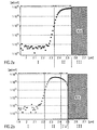
- Figures 2a and 2b illustrate dopant concentration profiles of a semiconductor substrate fabricated according to the first embodiment ( Figure 2a ) and a substrate fabricated according to the prior art method described further above ( Figure 2b ).
- Figure 2a illustrates the dopant concentration on the y axis versus a cross section of the substrate on the x axis.
- Region I of the dopant concentration corresponds to the second semiconductor layer 13 with a fairly constant dopant concentration of about 4 x 10 14 atoms/cm 3 .
- the second Region II corresponds to the modified first semiconductor layer 9 with a dopant concentration going up to 8 x 10 18 atoms/cm 3 .
- the highly doped layer 13 has actually a dopant profile which continuously, monotonically, increases and becomes rather flat towards the subsequent buried oxide layer (BOX). This layer has a thickness of 200 nm.
- the buried oxide insulating layer 5 is represented in Region III.
- the base substrate 3 was a silicon wafer.
- Figure 2b illustrates a dopant profile that is achieved with the prior art method in which a standard SOI substrate with a thin p- (or n-) semiconductor layer is used as starting material over which a further semiconductor layer with a p++ (n++) dopant concentration is provided.
- Region I illustrates the lowly doped semiconductor layer with its dopant concentration of the order of 7 x 10 14 atoms/cm 3 .
- Region II the highly doped layer has a dopant concentration going up to 7 x 10 18 atoms/cm 3 . Then follows the thin lowly doped semiconductor layer already present on the starting SOI substrate in Region IV.
- This layer is thus positioned between the Regions II and the buried oxide layer region III. Due to diffusion, the lowly doped thin semiconductor layer in Region IV has seen its dopant concentration increasing, so that, in the end, the dopant profile of the highly doped layer in Region II first grows (seen from Region I) and then decreases again towards the buried oxide layer. Comparing the two profiles, it appears the for the desired optoelectronic applications, the profile illustrated in Figure 2a is preferable.
- the steps illustrated in Figures 1b and 1c are carried out in the same device, namely in the epi-reactor 15, so that, in Figure 1b instead of doping of the first semiconductor layer 7 in an additional diffusion chamber 11, doping is carried out in the epi-reactor 15.
- This has the advantage that only one tool needs to be provided instead of two.
- the overall fabrication process is easier to carry out as in the epi-reactor, one wafer after the other is treated, whereas in the diffusion chamber 11. approximately 100 wafers are treated at the same time.
- the present invention brings the advantage that dopant cross-contamination risk between lowly doped and highly doped SOI wafers within one manufacturing line can be eliminated and furthermore, due to the doping of the first semiconductor layers 7 in an own doping step, a tailor-made dopant profile can be achieved which is independent of the starting SOI material.
- the starting material is a standard SOI substrate with a p- semiconductor layer over which a p++/n++ first semiconductor layer is epitaxially grown and over which in turn the p-/n- second layer will be grown is that, with the inventive method, a higher doping concentration can be achieved inside the p++/n++ modified first semiconductor layer 9 and, in addition, the concentration profile in the p++/n++ layer 9 can be kept essentially flat or at least evolves monotonically over its thickness (see figure 2a ), whereas it decreases and then increases within the p++/n++ layer with prior art technique (see figure 2b ).
Landscapes
- Recrystallisation Techniques (AREA)
Abstract
Description
- The invention relates to a method for fabricating a semiconductor substrate starting from a silicon on insulator (SOI) type substrate.
- In the optoelectronics, special substrates are needed which are for example used for image sensors, which find their application in video or photographic cameras. In these substrates, which are based on SOI type substrates, a buried oxide (BOX) is provided on a base through which photons can be collected from the backside of the wafer. Alternatively, the image sensors formed in the device layer of the SOI substrate could be transferred to a final substrate to expose the backside of the sensors. A thin highly doped p++(or n++) first semiconductor layer is directly provided on the buried oxide and a second semiconductor layer with a lower dopant concentration (p-/n- layer) is provided on the first semiconductor layer.
- In the prior art, this kind of special substrate was prepared using a highly doped substrate as the donor wafer in the conventional Smartcut™ technology. This method typically comprises the steps of providing a donor substrate, e.g. a silicon wafer, providing an insulating layer on the donor substrate and creating a predetermined splitting area inside the donor substrate, which is achieved by implanting atomic species or ions, like helium or hydrogen ions, into the donor substrate. In the next step the donor substrate is bonded to a base substrate, e.g. a further silicon wafer, such the insulating layer is sandwiched between handle and donor substrate. Subsequently, the remainder of the donor substrate is detached from the bonded donor-base substrate at the predetermined splitting area following a thermal and/or mechanical treatment upon the predetermined splitting area. As a result a semiconductor on insulator (SOI) substrate is obtained. Document
US-A-5137 837 describes a SOI-based semiconductor substrate. - However, the use of a highly doped substrate can lead to the following problem: It can be observed that cross-contamination from one donor wafer, e.g. with a high dopant concentration, to another wafer, e.g. with a lower dopant concentration like in the standard SOI substrates, occurs within the production line. This leads to unsatisfying dopant profiles in both the p++ type SOI wafers and the standard p- SOI wafers. In addition, during subsequent annealing steps during the Smartcut™ process, a diffusion of dopants out of the highly doped layer occurs which further deteriorates the substrate.
- According to an alternative method a standard SOI substrate with a thin p- (or n-) semiconductor layer was used as starting material over which a further semiconductor layer with a p++ dopant concentration was provided. Finally, an additional semiconductor layer with p- concentration was provided to obtain the desired layer structure. With this method it is, however, not possible to reach a sufficient high dopant concentration in the p++ layer and furthermore the dopant concentration is not sufficiently flat, meaning that that the dopant concentration through the layer is not monotonic, but first increasing and then decreasing within the p++ layer.
- Starting therefrom, it is the object of the present invention to provide a semiconductor substrate manufacturing process with which improved semiconductor substrates of the above described type can be achieved, thus which represent an improved dopant profile, in particular, in the highly doped p++ layer.
- This object is achieved with the method according to claim 1. This method comprises the steps of: a) providing a silicon on insulator (SOI) type substrate comprising a base, an insulating layer and a first semiconductor layer, b) doping the first semiconductor layer to thereby obtain a modified first semiconductor layer, and c) providing a second semiconductor layer with a different dopant concentration than the modified first semiconductor layer over, in particular on, the modified first semiconductor layer, steps b) and c) are carried out in the same fabrication device. In particular an epi-reactor.
- With this method an improved semiconductor substrate can be achieved as, the dopant concentration of the modified first semiconductor layer is established only once the SOI type substrate itself has been prepared. Thus, during the fabrication process of the SOI substrate itself, the same kind of donor substrates like in the standard procedure can be provided. Therefore, no cross-contamination from donor wafers with different dopant concentrations is observed and the dopant profile can not be deteriorated by annealing steps in the SOI fabrication procedure.
- Preferably, the dopant concentration in the modified first semiconductor layer is higher than in the second semiconductor layer. Like already mentioned this kind of substrate plays an important role, in particular, in optoelectronic applications and with the improved dopant concentration profile which can be achieved with the inventive method, improved final products are obtained.
- Advantageously, the second semiconductor layer can be epitaxially grown over, in particular on, the modified first semiconductor layer. By doing so, the quality of the substrate can be further improved.
- Preferably, the modified first semiconductor layer can be a highly doped n++ or p++ semiconductor layer, thus with a dopant concentration in the range of 1017atoms/cm3 up to 1020atoms/cm3. Thus, with this method, the high dopant concentrations necessary for high quality image sensors can be achieved with an improved dopant concentration profile through the different layers.
- Preferably, in step c), the second semiconductor layer is provided as an n- or p-semiconductor layer. Dopant concentrations in the range of 1 x 10¹⁴ to 1 x 10¹⁶ atoms/cm3 can be achieved with a clear interface between the highly doped first semiconductor layer and the second semiconductor layer. Thus again, improved substrates can be achieved.
- The special provision of a diffusion chamber, which is usually used to dope semiconductor layers, becomes obsolete. Using an epi-reactor for both steps, thus facilitates the production line, due to the fact that one tool, like the diffusion chamber, is no longer part of the production line. In addition, in the epi-reactor the wafers are treated one by one, whereas in the diffusion chambers about 100 wafers are treated at a time.
- According to a preferable embodiment, the base can be out of a transparent material. For instance, quartz-type substrates can be employed to provide the transparency of the base substrate with respect to the visible wavelength range, which is necessary for optoelectronic applications.
- Advantageously, the (modified) first semiconductor layer can have a thickness in a range of 50 nm to 800 nm, preferably 55 nm to 200 nm and/or the second semiconductor layer can have a thickness in a range of up to 8 µm, and/or the insulating layer can have a thickness of 50 nm to 1500 nm, in particular 100 nm to 400 nm. With the advantageous method, it is possible to provide highly doped and lowly doped semiconductor layers within a wide range of thicknesses. In particular, it is possible to provide a thin highly doped layer in the presence of a thicker lowly doped layer while keeping the desired dopant profile.
- Preferably, step a) can comprise the steps of: a1) providing a donor substrate, a2) providing an insulating layer on the donor substrate, a3) creating a predetermined splitting area inside the donor substrate, a4) bonding the donor substrate to the handle substrate, and a5) detaching a remainder of the donor substrate from the bonded donor handle substrate at the predetermined splitting area to thereby form the SOI substrate. With this so called Smartcut™ technology, high quality SOI wafers can be achieved and which can serve in the advantages method, even in cases when only a part of the SOI substrate leaving the production line will be used to create the substrates according to this invention.
- As already mentioned above, the inventive methods allows to create a superior substrate which in turn will also improve the qualities of the final product, e.g. the image sensor which uses the substrate.
- Advantageous embodiments of the invention will be described in the following in relation to the Figures.
- Figures 1A - 1C
- illustrate the steps of one embodiment according to the inventive method for fabricating a semiconductor substrate, and
- Figures 2a - 2b
- illustrate a typical dopant concentration profile in a semiconductor substrate fabricated according to the invention in comparison to one fabricated according to the prior art process.
- According to step a) of the inventive method, a SOI type substrate 1 is provided as illustrated in
figure 1 a. One way to fabricate such a substrate 1 is the so called SmartCut™ technology. This method typically comprises the steps of providing a donor substrate, e.g. a silicon wafer or a transparent substrate like quartz, providing an insulating layer on the donor and/or on the base substrate and creating a predetermined splitting area inside the donor substrate, which is achieved by implanting atomic species or ions, like helium or hydrogen ions, into the donor substrate. In the next step the donor substrate is bonded to a base substrate, e.g. a further silicon wafer, such the insulating layer is sandwiched between handle and donor substrate. Subsequently, the remainder of the donor substrate is detached from the bonded donor-base substrate at the predetermined splitting area following a thermal and/or mechanical treatment upon the predetermined splitting area. As a result a semiconductor on insulator (SOI) substrate is obtained. With this method, the insulating layer finds itself between the semiconductor layer transferred from the donor substrate and the base substrate. This layer then forms the abovementioned buried oxide layer (BOX). - Accordingly the SOI type substrate 1 provided in step a) of the inventive method comprises a
base 3, typically silicon. However, depending on the application also other materials are suitable, like for example transparent materials, like quartz, which find their application in optoelectronic applications. - On the
base 3, or on the donor, aninsulating layer 5 is provided, which is typically a silicon dioxide. However, again other insulating materials like silicon nitride or a stack of layers might also form theinsulating layer 5. - Over the
insulating layer 5, afirst semiconductor layer 7 is provided, which is typically a silicon layer. However, also for this layer, other semiconductor materials like germanium might also be used. - The thickness of the insulating layer is from about 50 nm to 1500 nm, preferably in a range of 100 nm to 400 nm. The
semiconductor layer 7 typically has a thickness of 50 nm to 800 nm, preferably 55 nm to 200 nm - According to step b) of claim 1, illustrated in
figure 1b , the next step of the inventive method consists in doping thefirst semiconductor layer 7 to thereby obtain a modifiedfirst semiconductor layer 9. Typically, doping is carried out with boron or phosphorous atoms to obtain n-type or p-type kinds of doping in a flow of hydrogen with temperatures of about 900 - 1200°C, preferably 1100 - 1160°C and for a time duration of 30 seconds - 4 minutes. This treatment will turn a p- semiconductor layer into a p++ semiconductor layer with a dopant concentration of 1017 or more Atoms/cm3 and in case of n- semiconductor layer as first semiconductor layer to an n++ layer with a dopant concentration of 1017 or more Atoms/cm3. - The next step according to the invention (step c of claim 1) consists in providing a
second semiconductor layer 13 with a different dopant concentration than the one of the modifiedfirst semiconductor layer 9. This step is typically carried out in a epi-reactor 15 and will result insecond semiconductor layer 13 achieved by epitaxial growth on the modifiedfirst semiconductor layer 9. For a silicon layer, the used precursor gases can be TCS, DCS, or silane and for doping the layer, again boron or phosphorous n-type or p-type dopants are used. The growth typically takes place at a temperature of 1000 - 1200°C and a layer with a thickness of up to 8 µm can be achieved. The dopant concentration is of the order of 1 x 10¹⁴ to 1 x 10¹⁶ atoms/cm3. -
Figures 2a and 2b illustrate dopant concentration profiles of a semiconductor substrate fabricated according to the first embodiment (Figure 2a ) and a substrate fabricated according to the prior art method described further above (Figure 2b ). -
Figure 2a illustrates the dopant concentration on the y axis versus a cross section of the substrate on the x axis. Region I of the dopant concentration corresponds to thesecond semiconductor layer 13 with a fairly constant dopant concentration of about 4 x 10¹⁴ atoms/cm3. The second Region II corresponds to the modifiedfirst semiconductor layer 9 with a dopant concentration going up to 8 x 10¹⁸ atoms/cm3. The highly dopedlayer 13 has actually a dopant profile which continuously, monotonically, increases and becomes rather flat towards the subsequent buried oxide layer (BOX). This layer has a thickness of 200 nm. Then, the buriedoxide insulating layer 5 is represented in Region III. In the shown example, which was fabricated according to the invention, thebase substrate 3 was a silicon wafer. - In contrast thereto,
Figure 2b illustrates a dopant profile that is achieved with the prior art method in which a standard SOI substrate with a thin p- (or n-) semiconductor layer is used as starting material over which a further semiconductor layer with a p++ (n++) dopant concentration is provided. Like inFigure 1 , Region I illustrates the lowly doped semiconductor layer with its dopant concentration of the order of 7 x 10¹⁴ atoms/cm3. Subsequently, in Region II, the highly doped layer has a dopant concentration going up to 7 x 10¹⁸ atoms/cm3. Then follows the thin lowly doped semiconductor layer already present on the starting SOI substrate in Region IV. This layer is thus positioned between the Regions II and the buried oxide layer region III. Due to diffusion, the lowly doped thin semiconductor layer in Region IV has seen its dopant concentration increasing, so that, in the end, the dopant profile of the highly doped layer in Region II first grows (seen from Region I) and then decreases again towards the buried oxide layer. Comparing the two profiles, it appears the for the desired optoelectronic applications, the profile illustrated inFigure 2a is preferable. - According to a second inventive embodiment, the steps illustrated in
Figures 1b and 1c are carried out in the same device, namely in the epi-reactor 15, so that, inFigure 1b instead of doping of thefirst semiconductor layer 7 in anadditional diffusion chamber 11, doping is carried out in the epi-reactor 15. This has the advantage that only one tool needs to be provided instead of two. Furthermore, the overall fabrication process is easier to carry out as in the epi-reactor, one wafer after the other is treated, whereas in thediffusion chamber 11. approximately 100 wafers are treated at the same time. - With the described inventive method, the following advantages can be achieved with respect to the known methods in the prior art. With respect to the process for fabricating a semiconductor substrate which starts from a SOI substrate with a p++ or n++ first semiconductor layer, the present invention brings the advantage that dopant cross-contamination risk between lowly doped and highly doped SOI wafers within one manufacturing line can be eliminated and furthermore, due to the doping of the
first semiconductor layers 7 in an own doping step, a tailor-made dopant profile can be achieved which is independent of the starting SOI material. - With respect to the method in which the starting material is a standard SOI substrate with a p- semiconductor layer over which a p++/n++ first semiconductor layer is epitaxially grown and over which in turn the p-/n- second layer will be grown is that, with the inventive method, a higher doping concentration can be achieved inside the p++/n++ modified
first semiconductor layer 9 and, in addition, the concentration profile in the p++/n++ layer 9 can be kept essentially flat or at least evolves monotonically over its thickness (seefigure 2a ), whereas it decreases and then increases within the p++/n++ layer with prior art technique (seefigure 2b ). - Thus, with the inventive method, superior semiconductor substrates can be achieved, which find their application in optoelectronics, in particular in image sensors. With the inventive method it is furthermore possible to have a large process window in terms of doping species, which in addition do not depend on the starting SOI substrate, and to have tailor-made doping levels, which do not depend on the bulk material available.
Claims (8)
- Method for fabricating a semiconductor substrate comprising the steps of:a) providing a silicon on insulator type (SOI) substrate (1) comprising a base (3), an insulating layer (5) and a first semiconductor layer (7),b) doping the first semiconductor layer (7) to thereby obtain a modified first semiconductor layer (9), andc) providing a second semiconductor layer (13) with a different dopant concentration than the modified first semiconductor layer (9) over, in particular on, the modified first semiconductor layer (9), and characterised in that
step b) and c) are carried out in the same fabrication device (11), in particular an epi-reactor. - Method according to claim 1, wherein the dopant concentration in the modified first semiconductor layer (9) is higher than in the second semiconductor layer (13).
- Method according to claim 1 or 2, wherein the second semiconductor layer (13) is epitaxially grown over, in particular on, the modified first semiconductor layer (9).
- Method according to one of claims 1 to 3, wherein after doping, the modified first semiconductor layer (9) is a highly doped n++ or p++ semiconductor layer.
- Method according to one of claims 1 to 4, wherein in step c) the second semiconductor layer (13) is provided as a n- or p- semiconductor layer.
- Method according to one of claims 1 to 5, wherein the base (3) is out of a transparent material.
- Method according to one of claims 1 to 6, wherein the modified first semiconductor layer (7, 9) has a thickness in a range of 50nm to 800nm, preferably 55 nm to 200 nm, and/or the second semiconductor layer (13) has a thickness in a range of up to 8µm, and/or the insulating layer (5) has a thickness of 50nm to 1500nm, in particular 100nm to 400nm.
- Method according to one of claims 1 to 7, wherein step a) comprises:a1) providing a donor substrate and a base substrate,a2) providing an insulating layer on the donor substrate or a base substrate,a3) creating a predetermined splitting area inside the donor substrate,a4) bonding the donor substrate to the base substrate, anda5) detaching a remainder of the donor substrate from the bonded donor-base substrate at the predetermined splitting area to thereby transfer a layer of the donor substrate including the insulating layer onto the base substrate to form the SOI substrate.
Priority Applications (10)
| Application Number | Priority Date | Filing Date | Title |
|---|---|---|---|
| AT08290176T ATE509376T1 (en) | 2008-02-26 | 2008-02-26 | METHOD FOR PRODUCING A SEMICONDUCTOR SUBSTRATE |
| EP08290176A EP2096683B1 (en) | 2008-02-26 | 2008-02-26 | Method for fabricating a semiconductor substrate |
| EP09715749A EP2255395B1 (en) | 2008-02-26 | 2009-02-26 | Method for fabricating a semiconductor substrate |
| CN201210068928.4A CN102623470B (en) | 2008-02-26 | 2009-02-26 | Manufacture the method for Semiconductor substrate |
| KR1020107015399A KR101595307B1 (en) | 2008-02-26 | 2009-02-26 | Method for fabricating a semiconductor substrate |
| CN2009801014367A CN101904017A (en) | 2008-02-26 | 2009-02-26 | Method for manufacturing semiconductor substrate |
| US12/918,935 US8575010B2 (en) | 2008-02-26 | 2009-02-26 | Method for fabricating a semiconductor substrate |
| JP2010547127A JP4810649B2 (en) | 2008-02-26 | 2009-02-26 | Method for manufacturing a semiconductor substrate |
| PCT/EP2009/001382 WO2009106330A1 (en) | 2008-02-26 | 2009-02-26 | Method for fabricating a semiconductor substrate |
| AT09715749T ATE555505T1 (en) | 2008-02-26 | 2009-02-26 | METHOD FOR PRODUCING A SEMICONDUCTOR SUBSTRATE |
Applications Claiming Priority (1)
| Application Number | Priority Date | Filing Date | Title |
|---|---|---|---|
| EP08290176A EP2096683B1 (en) | 2008-02-26 | 2008-02-26 | Method for fabricating a semiconductor substrate |
Publications (2)
| Publication Number | Publication Date |
|---|---|
| EP2096683A1 EP2096683A1 (en) | 2009-09-02 |
| EP2096683B1 true EP2096683B1 (en) | 2011-05-11 |
Family
ID=39658591
Family Applications (1)
| Application Number | Title | Priority Date | Filing Date |
|---|---|---|---|
| EP08290176A Active EP2096683B1 (en) | 2008-02-26 | 2008-02-26 | Method for fabricating a semiconductor substrate |
Country Status (2)
| Country | Link |
|---|---|
| EP (1) | EP2096683B1 (en) |
| AT (1) | ATE509376T1 (en) |
Family Cites Families (3)
| Publication number | Priority date | Publication date | Assignee | Title |
|---|---|---|---|---|
| US5137837A (en) * | 1990-08-20 | 1992-08-11 | Hughes Aircraft Company | Radiation-hard, high-voltage semiconductive device structure fabricated on SOI substrate |
| US6326280B1 (en) * | 1995-02-02 | 2001-12-04 | Sony Corporation | Thin film semiconductor and method for making thin film semiconductor |
| AU2003294822A1 (en) * | 2002-12-09 | 2004-06-30 | Quantum Semiconductor Llc | Cmos image sensor |
-
2008
- 2008-02-26 EP EP08290176A patent/EP2096683B1/en active Active
- 2008-02-26 AT AT08290176T patent/ATE509376T1/en not_active IP Right Cessation
Also Published As
| Publication number | Publication date |
|---|---|
| EP2096683A1 (en) | 2009-09-02 |
| ATE509376T1 (en) | 2011-05-15 |
Similar Documents
| Publication | Publication Date | Title |
|---|---|---|
| EP2202795A1 (en) | Method for fabricating a semiconductor substrate and semiconductor substrate | |
| US8318575B2 (en) | Compressive polycrystalline silicon film and method of manufacture thereof | |
| WO2005078786A1 (en) | Method of forming thin sgoi wafers with high relaxation and low stacking fault defect density | |
| CN112635611B (en) | Method for producing at least one tensile-strained planar photodiode | |
| EP2255395B1 (en) | Method for fabricating a semiconductor substrate | |
| US8617938B2 (en) | Device and method for boron diffusion in semiconductors | |
| JP2010153815A6 (en) | Semiconductor substrate manufacturing method and semiconductor substrate | |
| EP3304586B1 (en) | A method of manufacturing silicon germanium-on-insulator | |
| KR101698434B1 (en) | Method for fabricating a semiconductor substrate | |
| US11127775B2 (en) | Substrate for front side type imager and method of manufacturing such a substrate | |
| US12198975B2 (en) | Semiconductor on insulator structure for a front side type imager | |
| EP2096683A1 (en) | Method for fabricating a semiconductor substrate | |
| US7560318B2 (en) | Process for forming an electronic device including semiconductor layers having different stresses |
Legal Events
| Date | Code | Title | Description |
|---|---|---|---|
| PUAI | Public reference made under article 153(3) epc to a published international application that has entered the european phase |
Free format text: ORIGINAL CODE: 0009012 |
|
| AK | Designated contracting states |
Kind code of ref document: A1 Designated state(s): AT BE BG CH CY CZ DE DK EE ES FI FR GB GR HR HU IE IS IT LI LT LU LV MC MT NL NO PL PT RO SE SI SK TR |
|
| AX | Request for extension of the european patent |
Extension state: AL BA MK RS |
|
| 17P | Request for examination filed |
Effective date: 20100302 |
|
| 17Q | First examination report despatched |
Effective date: 20100409 |
|
| AKX | Designation fees paid |
Designated state(s): AT BE BG CH CY CZ DE DK EE ES FI FR GB GR HR HU IE IS IT LI LT LU LV MC MT NL NO PL PT RO SE SI SK TR |
|
| GRAP | Despatch of communication of intention to grant a patent |
Free format text: ORIGINAL CODE: EPIDOSNIGR1 |
|
| GRAS | Grant fee paid |
Free format text: ORIGINAL CODE: EPIDOSNIGR3 |
|
| GRAA | (expected) grant |
Free format text: ORIGINAL CODE: 0009210 |
|
| AK | Designated contracting states |
Kind code of ref document: B1 Designated state(s): AT BE BG CH CY CZ DE DK EE ES FI FR GB GR HR HU IE IS IT LI LT LU LV MC MT NL NO PL PT RO SE SI SK TR |
|
| REG | Reference to a national code |
Ref country code: GB Ref legal event code: FG4D |
|
| REG | Reference to a national code |
Ref country code: CH Ref legal event code: EP |
|
| REG | Reference to a national code |
Ref country code: IE Ref legal event code: FG4D |
|
| REG | Reference to a national code |
Ref country code: DE Ref legal event code: R096 Ref document number: 602008006843 Country of ref document: DE Effective date: 20110622 |
|
| REG | Reference to a national code |
Ref country code: NL Ref legal event code: T3 |
|
| PG25 | Lapsed in a contracting state [announced via postgrant information from national office to epo] |
Ref country code: SE Free format text: LAPSE BECAUSE OF FAILURE TO SUBMIT A TRANSLATION OF THE DESCRIPTION OR TO PAY THE FEE WITHIN THE PRESCRIBED TIME-LIMIT Effective date: 20110511 Ref country code: LT Free format text: LAPSE BECAUSE OF FAILURE TO SUBMIT A TRANSLATION OF THE DESCRIPTION OR TO PAY THE FEE WITHIN THE PRESCRIBED TIME-LIMIT Effective date: 20110511 Ref country code: NO Free format text: LAPSE BECAUSE OF FAILURE TO SUBMIT A TRANSLATION OF THE DESCRIPTION OR TO PAY THE FEE WITHIN THE PRESCRIBED TIME-LIMIT Effective date: 20110811 Ref country code: PT Free format text: LAPSE BECAUSE OF FAILURE TO SUBMIT A TRANSLATION OF THE DESCRIPTION OR TO PAY THE FEE WITHIN THE PRESCRIBED TIME-LIMIT Effective date: 20110912 |
|
| PG25 | Lapsed in a contracting state [announced via postgrant information from national office to epo] |
Ref country code: LV Free format text: LAPSE BECAUSE OF FAILURE TO SUBMIT A TRANSLATION OF THE DESCRIPTION OR TO PAY THE FEE WITHIN THE PRESCRIBED TIME-LIMIT Effective date: 20110511 Ref country code: IS Free format text: LAPSE BECAUSE OF FAILURE TO SUBMIT A TRANSLATION OF THE DESCRIPTION OR TO PAY THE FEE WITHIN THE PRESCRIBED TIME-LIMIT Effective date: 20110911 Ref country code: CY Free format text: LAPSE BECAUSE OF FAILURE TO SUBMIT A TRANSLATION OF THE DESCRIPTION OR TO PAY THE FEE WITHIN THE PRESCRIBED TIME-LIMIT Effective date: 20110511 Ref country code: GR Free format text: LAPSE BECAUSE OF FAILURE TO SUBMIT A TRANSLATION OF THE DESCRIPTION OR TO PAY THE FEE WITHIN THE PRESCRIBED TIME-LIMIT Effective date: 20110812 Ref country code: FI Free format text: LAPSE BECAUSE OF FAILURE TO SUBMIT A TRANSLATION OF THE DESCRIPTION OR TO PAY THE FEE WITHIN THE PRESCRIBED TIME-LIMIT Effective date: 20110511 Ref country code: BE Free format text: LAPSE BECAUSE OF FAILURE TO SUBMIT A TRANSLATION OF THE DESCRIPTION OR TO PAY THE FEE WITHIN THE PRESCRIBED TIME-LIMIT Effective date: 20110511 Ref country code: AT Free format text: LAPSE BECAUSE OF FAILURE TO SUBMIT A TRANSLATION OF THE DESCRIPTION OR TO PAY THE FEE WITHIN THE PRESCRIBED TIME-LIMIT Effective date: 20110511 Ref country code: SI Free format text: LAPSE BECAUSE OF FAILURE TO SUBMIT A TRANSLATION OF THE DESCRIPTION OR TO PAY THE FEE WITHIN THE PRESCRIBED TIME-LIMIT Effective date: 20110511 Ref country code: ES Free format text: LAPSE BECAUSE OF FAILURE TO SUBMIT A TRANSLATION OF THE DESCRIPTION OR TO PAY THE FEE WITHIN THE PRESCRIBED TIME-LIMIT Effective date: 20110822 |
|
| PG25 | Lapsed in a contracting state [announced via postgrant information from national office to epo] |
Ref country code: EE Free format text: LAPSE BECAUSE OF FAILURE TO SUBMIT A TRANSLATION OF THE DESCRIPTION OR TO PAY THE FEE WITHIN THE PRESCRIBED TIME-LIMIT Effective date: 20110511 Ref country code: CZ Free format text: LAPSE BECAUSE OF FAILURE TO SUBMIT A TRANSLATION OF THE DESCRIPTION OR TO PAY THE FEE WITHIN THE PRESCRIBED TIME-LIMIT Effective date: 20110511 |
|
| PG25 | Lapsed in a contracting state [announced via postgrant information from national office to epo] |
Ref country code: PL Free format text: LAPSE BECAUSE OF FAILURE TO SUBMIT A TRANSLATION OF THE DESCRIPTION OR TO PAY THE FEE WITHIN THE PRESCRIBED TIME-LIMIT Effective date: 20110511 Ref country code: DK Free format text: LAPSE BECAUSE OF FAILURE TO SUBMIT A TRANSLATION OF THE DESCRIPTION OR TO PAY THE FEE WITHIN THE PRESCRIBED TIME-LIMIT Effective date: 20110511 Ref country code: RO Free format text: LAPSE BECAUSE OF FAILURE TO SUBMIT A TRANSLATION OF THE DESCRIPTION OR TO PAY THE FEE WITHIN THE PRESCRIBED TIME-LIMIT Effective date: 20110511 Ref country code: SK Free format text: LAPSE BECAUSE OF FAILURE TO SUBMIT A TRANSLATION OF THE DESCRIPTION OR TO PAY THE FEE WITHIN THE PRESCRIBED TIME-LIMIT Effective date: 20110511 |
|
| PLBE | No opposition filed within time limit |
Free format text: ORIGINAL CODE: 0009261 |
|
| STAA | Information on the status of an ep patent application or granted ep patent |
Free format text: STATUS: NO OPPOSITION FILED WITHIN TIME LIMIT |
|
| 26N | No opposition filed |
Effective date: 20120214 |
|
| PG25 | Lapsed in a contracting state [announced via postgrant information from national office to epo] |
Ref country code: HR Free format text: LAPSE BECAUSE OF FAILURE TO SUBMIT A TRANSLATION OF THE DESCRIPTION OR TO PAY THE FEE WITHIN THE PRESCRIBED TIME-LIMIT Effective date: 20111123 |
|
| REG | Reference to a national code |
Ref country code: DE Ref legal event code: R097 Ref document number: 602008006843 Country of ref document: DE Effective date: 20120214 |
|
| PGFP | Annual fee paid to national office [announced via postgrant information from national office to epo] |
Ref country code: IT Payment date: 20120128 Year of fee payment: 5 |
|
| REG | Reference to a national code |
Ref country code: DE Ref legal event code: R082 Ref document number: 602008006843 Country of ref document: DE Representative=s name: GRUENECKER, KINKELDEY, STOCKMAIR & SCHWANHAEUS, DE |
|
| PG25 | Lapsed in a contracting state [announced via postgrant information from national office to epo] |
Ref country code: MC Free format text: LAPSE BECAUSE OF NON-PAYMENT OF DUE FEES Effective date: 20120229 |
|
| REG | Reference to a national code |
Ref country code: CH Ref legal event code: PL |
|
| REG | Reference to a national code |
Ref country code: DE Ref legal event code: R082 Ref document number: 602008006843 Country of ref document: DE Representative=s name: GRUENECKER, KINKELDEY, STOCKMAIR & SCHWANHAEUS, DE Effective date: 20120905 Ref country code: DE Ref legal event code: R081 Ref document number: 602008006843 Country of ref document: DE Owner name: SOITEC, FR Free format text: FORMER OWNER: S.O.I. TEC SILICON, BERNIN, FR Effective date: 20120905 Ref country code: DE Ref legal event code: R082 Ref document number: 602008006843 Country of ref document: DE Representative=s name: GRUENECKER PATENT- UND RECHTSANWAELTE PARTG MB, DE Effective date: 20120905 |
|
| PG25 | Lapsed in a contracting state [announced via postgrant information from national office to epo] |
Ref country code: LI Free format text: LAPSE BECAUSE OF NON-PAYMENT OF DUE FEES Effective date: 20120229 Ref country code: CH Free format text: LAPSE BECAUSE OF NON-PAYMENT OF DUE FEES Effective date: 20120229 |
|
| REG | Reference to a national code |
Ref country code: IE Ref legal event code: MM4A |
|
| PG25 | Lapsed in a contracting state [announced via postgrant information from national office to epo] |
Ref country code: IE Free format text: LAPSE BECAUSE OF NON-PAYMENT OF DUE FEES Effective date: 20120226 |
|
| REG | Reference to a national code |
Ref country code: FR Ref legal event code: RM Effective date: 20130107 Ref country code: FR Ref legal event code: CD Owner name: SOITEC, FR Effective date: 20130107 |
|
| PG25 | Lapsed in a contracting state [announced via postgrant information from national office to epo] |
Ref country code: BG Free format text: LAPSE BECAUSE OF FAILURE TO SUBMIT A TRANSLATION OF THE DESCRIPTION OR TO PAY THE FEE WITHIN THE PRESCRIBED TIME-LIMIT Effective date: 20110811 |
|
| PG25 | Lapsed in a contracting state [announced via postgrant information from national office to epo] |
Ref country code: MT Free format text: LAPSE BECAUSE OF FAILURE TO SUBMIT A TRANSLATION OF THE DESCRIPTION OR TO PAY THE FEE WITHIN THE PRESCRIBED TIME-LIMIT Effective date: 20110511 |
|
| PG25 | Lapsed in a contracting state [announced via postgrant information from national office to epo] |
Ref country code: HR Free format text: LAPSE BECAUSE OF FAILURE TO SUBMIT A TRANSLATION OF THE DESCRIPTION OR TO PAY THE FEE WITHIN THE PRESCRIBED TIME-LIMIT Effective date: 20110511 |
|
| PG25 | Lapsed in a contracting state [announced via postgrant information from national office to epo] |
Ref country code: IT Free format text: LAPSE BECAUSE OF NON-PAYMENT OF DUE FEES Effective date: 20130226 |
|
| PG25 | Lapsed in a contracting state [announced via postgrant information from national office to epo] |
Ref country code: TR Free format text: LAPSE BECAUSE OF FAILURE TO SUBMIT A TRANSLATION OF THE DESCRIPTION OR TO PAY THE FEE WITHIN THE PRESCRIBED TIME-LIMIT Effective date: 20110511 |
|
| PG25 | Lapsed in a contracting state [announced via postgrant information from national office to epo] |
Ref country code: LU Free format text: LAPSE BECAUSE OF NON-PAYMENT OF DUE FEES Effective date: 20120226 |
|
| PG25 | Lapsed in a contracting state [announced via postgrant information from national office to epo] |
Ref country code: HU Free format text: LAPSE BECAUSE OF FAILURE TO SUBMIT A TRANSLATION OF THE DESCRIPTION OR TO PAY THE FEE WITHIN THE PRESCRIBED TIME-LIMIT Effective date: 20080226 |
|
| REG | Reference to a national code |
Ref country code: FR Ref legal event code: PLFP Year of fee payment: 9 |
|
| REG | Reference to a national code |
Ref country code: FR Ref legal event code: PLFP Year of fee payment: 10 |
|
| REG | Reference to a national code |
Ref country code: FR Ref legal event code: PLFP Year of fee payment: 11 |
|
| REG | Reference to a national code |
Ref country code: DE Ref legal event code: R079 Ref document number: 602008006843 Country of ref document: DE Free format text: PREVIOUS MAIN CLASS: H01L0031180000 Ipc: H10F0071000000 |
|
| PGFP | Annual fee paid to national office [announced via postgrant information from national office to epo] |
Ref country code: NL Payment date: 20260106 Year of fee payment: 19 |
|
| PGFP | Annual fee paid to national office [announced via postgrant information from national office to epo] |
Ref country code: GB Payment date: 20260106 Year of fee payment: 19 |
|
| PGFP | Annual fee paid to national office [announced via postgrant information from national office to epo] |
Ref country code: DE Payment date: 20260102 Year of fee payment: 19 |
|
| PGFP | Annual fee paid to national office [announced via postgrant information from national office to epo] |
Ref country code: FR Payment date: 20260121 Year of fee payment: 19 |