EP2096677A2 - Semiconductor device and method of manufacturing the same - Google Patents
Semiconductor device and method of manufacturing the same Download PDFInfo
- Publication number
- EP2096677A2 EP2096677A2 EP09153700A EP09153700A EP2096677A2 EP 2096677 A2 EP2096677 A2 EP 2096677A2 EP 09153700 A EP09153700 A EP 09153700A EP 09153700 A EP09153700 A EP 09153700A EP 2096677 A2 EP2096677 A2 EP 2096677A2
- Authority
- EP
- European Patent Office
- Prior art keywords
- region
- conductivity type
- insulating film
- trench regions
- semiconductor device
- Prior art date
- Legal status (The legal status is an assumption and is not a legal conclusion. Google has not performed a legal analysis and makes no representation as to the accuracy of the status listed.)
- Withdrawn
Links
Images


Classifications
-
- H—ELECTRICITY
- H10—SEMICONDUCTOR DEVICES; ELECTRIC SOLID-STATE DEVICES NOT OTHERWISE PROVIDED FOR
- H10D—INORGANIC ELECTRIC SEMICONDUCTOR DEVICES
- H10D64/00—Electrodes of devices having potential barriers
- H10D64/20—Electrodes characterised by their shapes, relative sizes or dispositions
- H10D64/23—Electrodes carrying the current to be rectified, amplified, oscillated or switched, e.g. sources, drains, anodes or cathodes
- H10D64/251—Source or drain electrodes for field-effect devices
- H10D64/256—Source or drain electrodes for field-effect devices for lateral devices wherein the source or drain electrodes are recessed in semiconductor bodies
-
- H—ELECTRICITY
- H10—SEMICONDUCTOR DEVICES; ELECTRIC SOLID-STATE DEVICES NOT OTHERWISE PROVIDED FOR
- H10D—INORGANIC ELECTRIC SEMICONDUCTOR DEVICES
- H10D30/00—Field-effect transistors [FET]
- H10D30/60—Insulated-gate field-effect transistors [IGFET]
-
- H—ELECTRICITY
- H10—SEMICONDUCTOR DEVICES; ELECTRIC SOLID-STATE DEVICES NOT OTHERWISE PROVIDED FOR
- H10D—INORGANIC ELECTRIC SEMICONDUCTOR DEVICES
- H10D30/00—Field-effect transistors [FET]
- H10D30/60—Insulated-gate field-effect transistors [IGFET]
- H10D30/63—Vertical IGFETs
-
- H—ELECTRICITY
- H10—SEMICONDUCTOR DEVICES; ELECTRIC SOLID-STATE DEVICES NOT OTHERWISE PROVIDED FOR
- H10D—INORGANIC ELECTRIC SEMICONDUCTOR DEVICES
- H10D30/00—Field-effect transistors [FET]
- H10D30/60—Insulated-gate field-effect transistors [IGFET]
- H10D30/64—Double-diffused metal-oxide semiconductor [DMOS] FETs
- H10D30/65—Lateral DMOS [LDMOS] FETs
- H10D30/658—Lateral DMOS [LDMOS] FETs having trench gate electrodes
-
- H—ELECTRICITY
- H10—SEMICONDUCTOR DEVICES; ELECTRIC SOLID-STATE DEVICES NOT OTHERWISE PROVIDED FOR
- H10D—INORGANIC ELECTRIC SEMICONDUCTOR DEVICES
- H10D30/00—Field-effect transistors [FET]
- H10D30/60—Insulated-gate field-effect transistors [IGFET]
- H10D30/64—Double-diffused metal-oxide semiconductor [DMOS] FETs
- H10D30/66—Vertical DMOS [VDMOS] FETs
- H10D30/668—Vertical DMOS [VDMOS] FETs having trench gate electrodes, e.g. UMOS transistors
-
- H—ELECTRICITY
- H10—SEMICONDUCTOR DEVICES; ELECTRIC SOLID-STATE DEVICES NOT OTHERWISE PROVIDED FOR
- H10D—INORGANIC ELECTRIC SEMICONDUCTOR DEVICES
- H10D64/00—Electrodes of devices having potential barriers
- H10D64/01—Manufacture or treatment
- H10D64/025—Manufacture or treatment forming recessed gates, e.g. by using local oxidation
- H10D64/027—Manufacture or treatment forming recessed gates, e.g. by using local oxidation by etching at gate locations
-
- H—ELECTRICITY
- H10—SEMICONDUCTOR DEVICES; ELECTRIC SOLID-STATE DEVICES NOT OTHERWISE PROVIDED FOR
- H10D—INORGANIC ELECTRIC SEMICONDUCTOR DEVICES
- H10D64/00—Electrodes of devices having potential barriers
- H10D64/20—Electrodes characterised by their shapes, relative sizes or dispositions
- H10D64/27—Electrodes not carrying the current to be rectified, amplified, oscillated or switched, e.g. gates
- H10D64/311—Gate electrodes for field-effect devices
- H10D64/411—Gate electrodes for field-effect devices for FETs
- H10D64/511—Gate electrodes for field-effect devices for FETs for IGFETs
-
- H—ELECTRICITY
- H10—SEMICONDUCTOR DEVICES; ELECTRIC SOLID-STATE DEVICES NOT OTHERWISE PROVIDED FOR
- H10D—INORGANIC ELECTRIC SEMICONDUCTOR DEVICES
- H10D64/00—Electrodes of devices having potential barriers
- H10D64/20—Electrodes characterised by their shapes, relative sizes or dispositions
- H10D64/27—Electrodes not carrying the current to be rectified, amplified, oscillated or switched, e.g. gates
- H10D64/311—Gate electrodes for field-effect devices
- H10D64/411—Gate electrodes for field-effect devices for FETs
- H10D64/511—Gate electrodes for field-effect devices for FETs for IGFETs
- H10D64/512—Disposition of the gate electrodes, e.g. buried gates
- H10D64/513—Disposition of the gate electrodes, e.g. buried gates within recesses in the substrate, e.g. trench gates, groove gates or buried gates
-
- H—ELECTRICITY
- H10—SEMICONDUCTOR DEVICES; ELECTRIC SOLID-STATE DEVICES NOT OTHERWISE PROVIDED FOR
- H10D—INORGANIC ELECTRIC SEMICONDUCTOR DEVICES
- H10D62/00—Semiconductor bodies, or regions thereof, of devices having potential barriers
- H10D62/10—Shapes, relative sizes or dispositions of the regions of the semiconductor bodies; Shapes of the semiconductor bodies
- H10D62/13—Semiconductor regions connected to electrodes carrying current to be rectified, amplified or switched, e.g. source or drain regions
- H10D62/149—Source or drain regions of field-effect devices
- H10D62/151—Source or drain regions of field-effect devices of IGFETs
- H10D62/156—Drain regions of DMOS transistors
- H10D62/158—Dispositions
-
- H—ELECTRICITY
- H10—SEMICONDUCTOR DEVICES; ELECTRIC SOLID-STATE DEVICES NOT OTHERWISE PROVIDED FOR
- H10D—INORGANIC ELECTRIC SEMICONDUCTOR DEVICES
- H10D64/00—Electrodes of devices having potential barriers
- H10D64/20—Electrodes characterised by their shapes, relative sizes or dispositions
- H10D64/23—Electrodes carrying the current to be rectified, amplified, oscillated or switched, e.g. sources, drains, anodes or cathodes
- H10D64/251—Source or drain electrodes for field-effect devices
- H10D64/257—Source or drain electrodes for field-effect devices for lateral devices wherein the source or drain electrodes are characterised by top-view geometrical layouts, e.g. interdigitated, semi-circular, annular or L-shaped electrodes
Definitions
- the present invention relates to a semiconductor device and a method of manufacturing a semiconductor device, for example, a metal oxide semiconductor (MOS) transistor.
- MOS metal oxide semiconductor
- the trench gate MOS transistor can be nominated as a mainstream structure at present in the field of power MOS field effect transistors (FETs) having a high withstanding voltage and high driving performance.
- FETs field effect transistors
- the trench gate MOS transistor has the highest scale in integration (for example, see JP 01-310576 A ).
- the trench gate MOS transistor shows extremely excellent performance as an element itself, however it is disadvantageous when being mounted on a chip together with other semiconductor elements since the trench gate MOS transistor has a vertical MOS structure, in which current flows in a depth direction of a substrate, and an entire rear surface of a semiconductor substrate is an electrode.
- the present invention has an object to provide a semiconductor device having a low on-resistance, which is capable of being mounted on a chip together with other semiconductor elements.
- the drain electrode is drawn from the inside of the trench and therefore the drain electrode can be taken from the surface of the semiconductor substrate, whereby on-chip mounting with other semiconductor elements can be achieved with ease.
- FIGS. 1A and 1B illustrate a structure of a semiconductor device according to an embodiment of the present invention.
- FIG. 1A is a top view
- FIG. 1B is a bird's-eye view and is cut out along a dotted-line portion of FIG. 1A .
- a plurality of trench regions 12 are formed in a first conductivity type well region 2 formed on a semiconductor substrate 1.
- a source electrode 10 has an ohmic contact with a second conductivity type source region 6 formed on a substrate surface between the trench regions 12. Adjacently to the second conductivity type source region 6, there is formed a first conductivity type high concentration region 11, which is brought into butting contact with the source electrode 10 together with the second conductivity type source region 6, whereby a substrate potential is fixed.
- a second conductivity type drain region 5 is formed at a bottom portion of the trench region 12, and a potential is taken to the substrate surface by a drain electrode 9 buried inside the trench region 12.
- An arbitrary voltage is applied to the drain electrode 9 and a gate electrode 4b made of metal which is connected to a gate electrode 4a formed continuously over a flat region on an outer side of the trench region 12 and a side wall inside the trench region 12, whereby carriers flow from the second conductivity type source region 6 to the second conductivity type drain region 5 in a direction indicated with an arrow 8, bringing the semiconductor device into an on-state.
- a gate length extends in a direction perpendicular to the surface of the semiconductor substrate, and hence an area efficiency is excellent compared with a planar type MOS transistor, resulting in enhancement of driving performance per unit area. Further, all the electrodes are exposed to the surface of the semiconductor substrate, and therefore on-chip mounting with other elements, which has been difficult to be achieved in the trench MOS transistor, is realized with ease.
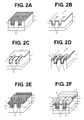
- FIGS. 2A to 2F are bird's-eye views of a process flow, illustrating the method of manufacturing the semiconductor device according to the basic embodiment of the present invention illustrated in FIGS. 1A and 1B .
- the first conductivity type well region 2 is formed on the semiconductor substrate 1 and then the trench regions 12 are formed in the first conductivity type well region 2 at a depth smaller than that of the first conductivity type well region 2. After that, thermal oxidation is performed to form a gate oxide film 3 on the substrate surface and inside the trench regions 12.
- the gate electrode film 4a is deposited on the gate oxide film 3 and, as illustrated in FIG. 2C , the gate electrode film 4a and the gate oxide film 3 are partially removed by highly anisotropic dry etching.
- the gate electrode film 4a and the gate oxide film 3 are all removed, but the gate electrode film 4a and the gate oxide film 3 deposited on a trench side wall are not removed by highly anisotropic dry etching.
- second conductivity type impurities are ion-implanted into a region excluding a region in which the first conductivity type high concentration region 11 is formed so that the second conductivity type drain region 5 and the second conductivity type source region 6 are formed in a self-aligning manner.
- the region excluding the region in which the first conductivity type high concentration region 11 is formed is masked with a resist or the like, whereby the first conductivity type high concentration region 11 is formed by ion-implantation or the like.
- an interlayer insulating film 7 is deposited. Thereafter, the interlayer insulating film 7 is subjected to selective etching in a part of regions of the second conductivity type drain region 5, the second conductivity type source region 6, the first conductivity type high concentration region 11, and the gate electrode 4a to thereby form openings.
- metal is deposited to be arbitrarily patterned, whereby the gate electrode 4b, the drain electrode 9, and the source electrode 10 are formed.
- an electric field relaxation region is formed in a drain region, whereby a withstanding voltage of a semiconductor device is enhanced.
- FIG. 3 is a conceptual view of the modification example.
- FIG. 3 illustrates a structure in which, in the basic structure of FIGS. 1A and 1B , a second conductivity type low concentration diffusion region 13 is formed between the semiconductor substrate 1 and the first conductivity type well region 2. This structure is realized by a manufacturing method such as a double diffusion or an epitaxial growth.
- the second conductivity type low concentration diffusion region 13 is formed, whereby an electric field applied to a drain can be mitigated and a drain withstanding voltage can be enhanced.
- the second conductivity type drain region 5 is set so as to be within the second conductivity type low concentration diffusion region 13, and a impurity concentration of the second conductivity type low concentration diffusion region 13 and a distance between the deepest bottom portion of the trench region 12 and a bottom portion of the first conductivity type well region 2 are arbitrarily adjusted based on a target withstanding voltage.
- the first conductivity type is set to p-type
- the second conductivity type is set to n-type, whereby the n-channel MOS transistor is described.
- this transistor functions as a p-channel MOS transistor.
Landscapes
- Insulated Gate Type Field-Effect Transistor (AREA)
- Electrodes Of Semiconductors (AREA)
Abstract
Description
- The present invention relates to a semiconductor device and a method of manufacturing a semiconductor device, for example, a metal oxide semiconductor (MOS) transistor.
- With full use of a microfabrication technology, with times, it becomes possible to manufacture semiconductor devices while achieving downsizing without decreasing performance thereof. This tendency is also found in semiconductor elements having high driving performance, and hence a reduction in on-resistance per unit area has been pursued by making full use of the microfabrication technology. However, in fact, a lowering of a withstanding voltage, which is caused by miniaturization of elements, hinders further enhancement of the driving performance owing to the microfabrication technology. In order to overcome the trade-off between the miniaturization and the withstanding voltage, there have been proposed elements having various structures, and the trench gate MOS transistor can be nominated as a mainstream structure at present in the field of power MOS field effect transistors (FETs) having a high withstanding voltage and high driving performance.
- Among doubled-diffused MOS (DMOS) transistors having a high withstanding voltage and high driving performance, the trench gate MOS transistor has the highest scale in integration (for example, see
JP 01-310576 A - The trench gate MOS transistor shows extremely excellent performance as an element itself, however it is disadvantageous when being mounted on a chip together with other semiconductor elements since the trench gate MOS transistor has a vertical MOS structure, in which current flows in a depth direction of a substrate, and an entire rear surface of a semiconductor substrate is an electrode.
- The present invention has an object to provide a semiconductor device having a low on-resistance, which is capable of being mounted on a chip together with other semiconductor elements.
- (1) According to the present invention, there is provided a semiconductor device including: a first conductivity type well region formed on a surface of a semiconductor substrate at an arbitrary depth; a plurality of trench regions formed at a depth smaller than the predetermined depth of the first conductivity type well region; a gate electrode disposed on a side surface of each the plurality of trench regions via a gate insulating film and brought into contact with the gate insulating film; a second conductivity type drain region formed in a bottom portion of each of the plurality of trench regions; a second conductivity type source region formed in a part of a region, which is formed between the plurality of trench regions, of the surface of the semiconductor substrate; and a first conductivity type high concentration region formed in a part of a region, which is formed between the plurality of trench regions, of the surface of the semiconductor substrate.
- (2) A semiconductor device according to item (1) may further include a second conductivity type low concentration diffusion region formed between the semiconductor substrate and the first conductivity type well region to surround the second conductivity type drain region.
- (3) According to the present invention, there is provided a method of manufacturing a semiconductor device including: forming a first conductivity type well region on a semiconductor substrate; forming a plurality of trench regions at a depth smaller than a depth of the first conductivity type well region; forming a gate insulating film; forming a gate electrode film; removing, by anisotropic etching, the gate insulating film and the gate electrode film formed on a bottom portion of each of the plurality of trench regions and a part of the gate insulating film and the gate electrode film formed on a surface of the semiconductor substrate between two of the plurality of trench regions; forming an interlayer insulating film; removing, by etching, a part of the interlayer insulating film formed on the gate electrode film, a part of the interlayer insulating film formed on the bottom portion of each of the plurality of trench regions, and a part of the interlayer insulating film formed on the surface of the semiconductor substrate between two of the plurality of trench regions; forming a metal film; and etching a part of the metal film.
- (4) A method of manufacturing a semiconductor device according to item (3) further includes forming a second conductivity type low concentration diffusion region.
- (5) A method of manufacturing a semiconductor device according to item (3) further includes performing an epitaxial growth.
- According to the present invention, the drain electrode is drawn from the inside of the trench and therefore the drain electrode can be taken from the surface of the semiconductor substrate, whereby on-chip mounting with other semiconductor elements can be achieved with ease.
- Embodiments of the present invention will now be described by way of further example only and with reference to the accompanying drawings, in which:
-
FIGS. 1A and 1B are views for describing a structure of a semiconductor device according to an embodiment of the present invention; -
FIGS. 2A to 2F are views for describing a method of manufacturing the semiconductor device according to the embodiment of the present invention; and -
FIG. 3 is a view for describing a modification example of the semiconductor device according to the embodiment of the present invention. -
FIGS. 1A and 1B illustrate a structure of a semiconductor device according to an embodiment of the present invention.FIG. 1A is a top view, andFIG. 1B is a bird's-eye view and is cut out along a dotted-line portion ofFIG. 1A . - A plurality of
trench regions 12 are formed in a first conductivitytype well region 2 formed on asemiconductor substrate 1. Asource electrode 10 has an ohmic contact with a second conductivitytype source region 6 formed on a substrate surface between thetrench regions 12. Adjacently to the second conductivitytype source region 6, there is formed a first conductivity typehigh concentration region 11, which is brought into butting contact with thesource electrode 10 together with the second conductivitytype source region 6, whereby a substrate potential is fixed. - A second conductivity
type drain region 5 is formed at a bottom portion of thetrench region 12, and a potential is taken to the substrate surface by adrain electrode 9 buried inside thetrench region 12. - An arbitrary voltage is applied to the
drain electrode 9 and agate electrode 4b made of metal which is connected to agate electrode 4a formed continuously over a flat region on an outer side of thetrench region 12 and a side wall inside thetrench region 12, whereby carriers flow from the second conductivitytype source region 6 to the second conductivitytype drain region 5 in a direction indicated with anarrow 8, bringing the semiconductor device into an on-state. - Specifically, as in a trench MOS transistor, a gate length extends in a direction perpendicular to the surface of the semiconductor substrate, and hence an area efficiency is excellent compared with a planar type MOS transistor, resulting in enhancement of driving performance per unit area. Further, all the electrodes are exposed to the surface of the semiconductor substrate, and therefore on-chip mounting with other elements, which has been difficult to be achieved in the trench MOS transistor, is realized with ease.
- Next, a method of manufacturing the semiconductor device is described.
-
FIGS. 2A to 2F are bird's-eye views of a process flow, illustrating the method of manufacturing the semiconductor device according to the basic embodiment of the present invention illustrated inFIGS. 1A and 1B . - First, as illustrated in
FIG. 2A , the first conductivitytype well region 2 is formed on thesemiconductor substrate 1 and then thetrench regions 12 are formed in the first conductivitytype well region 2 at a depth smaller than that of the first conductivitytype well region 2. After that, thermal oxidation is performed to form agate oxide film 3 on the substrate surface and inside thetrench regions 12. - Next, as illustrated in
FIG. 2B , thegate electrode film 4a is deposited on thegate oxide film 3 and, as illustrated inFIG. 2C , thegate electrode film 4a and thegate oxide film 3 are partially removed by highly anisotropic dry etching. In this case, as to the substrate surface and a trench bottom surface included in a region to be etched, thegate electrode film 4a and thegate oxide film 3 are all removed, but thegate electrode film 4a and thegate oxide film 3 deposited on a trench side wall are not removed by highly anisotropic dry etching. - As illustrated in
FIG. 2D , second conductivity type impurities are ion-implanted into a region excluding a region in which the first conductivity typehigh concentration region 11 is formed so that the second conductivitytype drain region 5 and the second conductivitytype source region 6 are formed in a self-aligning manner. After that, the region excluding the region in which the first conductivity typehigh concentration region 11 is formed is masked with a resist or the like, whereby the first conductivity typehigh concentration region 11 is formed by ion-implantation or the like. - Next, as illustrated in
FIG. 2E , an interlayerinsulating film 7 is deposited. Thereafter, theinterlayer insulating film 7 is subjected to selective etching in a part of regions of the second conductivitytype drain region 5, the second conductivitytype source region 6, the first conductivity typehigh concentration region 11, and thegate electrode 4a to thereby form openings. - Finally, as illustrated in
FIG. 2F , metal is deposited to be arbitrarily patterned, whereby thegate electrode 4b, thedrain electrode 9, and thesource electrode 10 are formed. - In this modification example, an electric field relaxation region is formed in a drain region, whereby a withstanding voltage of a semiconductor device is enhanced.
-
FIG. 3 is a conceptual view of the modification example.FIG. 3 illustrates a structure in which, in the basic structure ofFIGS. 1A and 1B , a second conductivity type lowconcentration diffusion region 13 is formed between thesemiconductor substrate 1 and the first conductivitytype well region 2. This structure is realized by a manufacturing method such as a double diffusion or an epitaxial growth. - As described above, the second conductivity type low
concentration diffusion region 13 is formed, whereby an electric field applied to a drain can be mitigated and a drain withstanding voltage can be enhanced. - In this case, the second conductivity
type drain region 5 is set so as to be within the second conductivity type lowconcentration diffusion region 13, and a impurity concentration of the second conductivity type lowconcentration diffusion region 13 and a distance between the deepest bottom portion of thetrench region 12 and a bottom portion of the first conductivitytype well region 2 are arbitrarily adjusted based on a target withstanding voltage. - Note that, in
FIGS. 1A and 1B ,2A to 2F , and3 , the first conductivity type is set to p-type, and the second conductivity type is set to n-type, whereby the n-channel MOS transistor is described. When the first conductivity type is set to n-type and the second conductivity type is set to p-type, this transistor functions as a p-channel MOS transistor. - The foregoing description has been given by way of example only and it will be appreciated by a person skilled in the art that modifications can be made without departing from the scope of the present invention.
Claims (5)
- A semiconductor device, comprising:a first conductivity type well region (2) disposed on a surface of a semiconductor substrate (1) at a predetermined depth;a plurality of trench regions (12) disposed at a depth smaller than the predetermined depth of the first conductivity type well region;a gate electrode (4a) disposed on a side surface of each of the plurality of trench regions via a gate insulating film (3) and brought into contact with the gate insulating film;a second conductivity type drain region (5) disposed in a bottom portion of each of the plurality of trench regions;a second conductivity type source region (6) disposed in a region formed between the plurality of trench regions, and disposed on the surface of the semiconductor substrate along the gate insulating film; anda first conductivity type high concentration region (11) disposed in a region formed between the plurality of trench regions, and disposed on the surface of the semiconductor substrate to be brought into contact with the second conductivity type source region.
- A semiconductor device according to claim 1, further comprising a second conductivity type low concentration diffusion region (13) formed between the semiconductor substrate (1) and the first conductivity type well region (2) to surround the second conductivity type drain region (5).
- A method of manufacturing a semiconductor device, comprising:forming a first conductivity type well region (2) on a semiconductor substrate (1);forming a plurality of trench regions (12) at a depth smaller than a depth of the first conductivity type well region;forming a gate insulating film (3);forming a gate electrode film (4a);removing, by anisotropic etching, the gate insulating film and the gate electrode film formed on a bottom portion of each of the plurality of trench regions and a part of the gate insulating film and the gate electrode film formed on a surface of the semiconductor substrate between two of the plurality of trench regions;forming an interlayer insulating film (7);removing, by etching, a part of the interlayer insulating film formed on the gate electrode film, a part of the interlayer insulating film formed on the bottom portion of each of the plurality of trench regions, and a part of the interlayer insulating film formed on the surface of the semiconductor substrate between two of the plurality of trench regions;forming a metal film (4b, 9, 10); andetching a part of the metal film.
- A method of manufacturing a semiconductor device according to claim 3, further comprising forming, before the forming the first conductivity type well region on the semiconductor substrate, a second conductivity type low concentration diffusion region (13) on an entire surface of a region on which a transistor is formed.
- A method of manufacturing a semiconductor device according to claim 4, wherein the forming the second conductivity type low concentration diffusion region on the entire surface of the region on which the transistor is formed comprises an epitaxial growth.
Applications Claiming Priority (1)
| Application Number | Priority Date | Filing Date | Title |
|---|---|---|---|
| JP2008046370A JP2009206268A (en) | 2008-02-27 | 2008-02-27 | Semiconductor device, and manufacturing method thereof |
Publications (2)
| Publication Number | Publication Date |
|---|---|
| EP2096677A2 true EP2096677A2 (en) | 2009-09-02 |
| EP2096677A3 EP2096677A3 (en) | 2009-10-14 |
Family
ID=40600263
Family Applications (1)
| Application Number | Title | Priority Date | Filing Date |
|---|---|---|---|
| EP09153700A Withdrawn EP2096677A3 (en) | 2008-02-27 | 2009-02-26 | Semiconductor device and method of manufacturing the same |
Country Status (6)
| Country | Link |
|---|---|
| US (2) | US7859049B2 (en) |
| EP (1) | EP2096677A3 (en) |
| JP (1) | JP2009206268A (en) |
| KR (1) | KR20090092718A (en) |
| CN (1) | CN101552292B (en) |
| TW (1) | TWI462291B (en) |
Cited By (2)
| Publication number | Priority date | Publication date | Assignee | Title |
|---|---|---|---|---|
| WO2018098334A1 (en) * | 2016-11-23 | 2018-05-31 | Microchip Technology Incorporated | Vertical field effect transistor with front-side source and drain contacts |
| WO2018098347A1 (en) * | 2016-11-23 | 2018-05-31 | Microchip Technology Incorporated | Method of forming a vertical field effect transistor with front-side source and drain contacts |
Families Citing this family (5)
| Publication number | Priority date | Publication date | Assignee | Title |
|---|---|---|---|---|
| KR100861213B1 (en) * | 2007-04-17 | 2008-09-30 | 동부일렉트로닉스 주식회사 | Semiconductor device and manufacturing method |
| WO2012077617A1 (en) | 2010-12-10 | 2012-06-14 | 三菱電機株式会社 | Semiconductor device and production method therefor |
| US8679919B2 (en) | 2011-12-15 | 2014-03-25 | Semiconductor Components Industries, Llc | Electronic device comprising a conductive structure and an insulating layer within a trench and a process of forming the same |
| US8647970B2 (en) * | 2011-12-15 | 2014-02-11 | Semiconductor Components Industries, Llc | Electronic device comprising conductive structures and an insulating layer between the conductive structures and within a trench |
| US8878287B1 (en) * | 2012-04-12 | 2014-11-04 | Micrel, Inc. | Split slot FET with embedded drain |
Citations (1)
| Publication number | Priority date | Publication date | Assignee | Title |
|---|---|---|---|---|
| JPH01310576A (en) | 1988-06-08 | 1989-12-14 | Mitsubishi Electric Corp | Semiconductor device and manufacture thereof |
Family Cites Families (15)
| Publication number | Priority date | Publication date | Assignee | Title |
|---|---|---|---|---|
| JP3395473B2 (en) * | 1994-10-25 | 2003-04-14 | 富士電機株式会社 | Horizontal trench MISFET and manufacturing method thereof |
| KR0165398B1 (en) * | 1995-05-26 | 1998-12-15 | 윤종용 | Vertical transistor manufacturing method |
| JP3252804B2 (en) * | 1998-07-31 | 2002-02-04 | 日本電気株式会社 | Driving method of solid-state imaging device |
| US6831294B1 (en) * | 1999-01-22 | 2004-12-14 | Renesas Technology Corp. | Semiconductor integrated circuit device having bump electrodes for signal or power only, and testing pads that are not coupled to bump electrodes |
| DE60040798D1 (en) * | 1999-10-27 | 2008-12-24 | Kansai Electric Power Co | Semiconductor device with drift regions of opposite conductivity types |
| JP2002141505A (en) * | 2000-10-31 | 2002-05-17 | Shindengen Electric Mfg Co Ltd | Field effect transistor |
| DE10223822A1 (en) * | 2001-05-30 | 2002-12-05 | Fuji Electric Co Ltd | Semiconductor component and method for its production |
| JP4461676B2 (en) * | 2001-12-18 | 2010-05-12 | 富士電機システムズ株式会社 | Manufacturing method of semiconductor device |
| JP4487481B2 (en) * | 2002-01-16 | 2010-06-23 | 富士電機システムズ株式会社 | Semiconductor device and manufacturing method thereof |
| US7372088B2 (en) * | 2004-01-27 | 2008-05-13 | Matsushita Electric Industrial Co., Ltd. | Vertical gate semiconductor device and method for fabricating the same |
| CN101567373B (en) * | 2004-02-16 | 2011-04-13 | 富士电机系统株式会社 | Bi-direction element and its manufacturing method |
| JP4765016B2 (en) * | 2004-04-06 | 2011-09-07 | 富士電機株式会社 | Manufacturing method of semiconductor device |
| JP4997694B2 (en) * | 2004-10-07 | 2012-08-08 | 富士電機株式会社 | Semiconductor device and manufacturing method thereof |
| US20070032029A1 (en) * | 2005-04-19 | 2007-02-08 | Rensselaer Polytechnic Institute | Lateral trench power MOSFET with reduced gate-to-drain capacitance |
| JP2008177335A (en) * | 2007-01-18 | 2008-07-31 | Fuji Electric Device Technology Co Ltd | Silicon carbide insulated gate type semiconductor device. |
-
2008
- 2008-02-27 JP JP2008046370A patent/JP2009206268A/en not_active Withdrawn
-
2009
- 2009-02-24 TW TW098105809A patent/TWI462291B/en not_active IP Right Cessation
- 2009-02-25 US US12/392,491 patent/US7859049B2/en not_active Expired - Fee Related
- 2009-02-26 EP EP09153700A patent/EP2096677A3/en not_active Withdrawn
- 2009-02-26 KR KR1020090016201A patent/KR20090092718A/en not_active Ceased
- 2009-02-27 CN CN2009101184317A patent/CN101552292B/en not_active Expired - Fee Related
-
2010
- 2010-11-18 US US12/949,434 patent/US8193060B2/en not_active Expired - Fee Related
Patent Citations (1)
| Publication number | Priority date | Publication date | Assignee | Title |
|---|---|---|---|---|
| JPH01310576A (en) | 1988-06-08 | 1989-12-14 | Mitsubishi Electric Corp | Semiconductor device and manufacture thereof |
Cited By (3)
| Publication number | Priority date | Publication date | Assignee | Title |
|---|---|---|---|---|
| WO2018098334A1 (en) * | 2016-11-23 | 2018-05-31 | Microchip Technology Incorporated | Vertical field effect transistor with front-side source and drain contacts |
| WO2018098347A1 (en) * | 2016-11-23 | 2018-05-31 | Microchip Technology Incorporated | Method of forming a vertical field effect transistor with front-side source and drain contacts |
| US10326013B2 (en) | 2016-11-23 | 2019-06-18 | Microchip Technology Incorporated | Method of forming a field-effect transistor (FET) or other semiconductor device with front-side source and drain contacts |
Also Published As
| Publication number | Publication date |
|---|---|
| US8193060B2 (en) | 2012-06-05 |
| US20090212357A1 (en) | 2009-08-27 |
| TW200945587A (en) | 2009-11-01 |
| US7859049B2 (en) | 2010-12-28 |
| CN101552292A (en) | 2009-10-07 |
| TWI462291B (en) | 2014-11-21 |
| KR20090092718A (en) | 2009-09-01 |
| EP2096677A3 (en) | 2009-10-14 |
| JP2009206268A (en) | 2009-09-10 |
| CN101552292B (en) | 2013-03-27 |
| US20110065247A1 (en) | 2011-03-17 |
Similar Documents
| Publication | Publication Date | Title |
|---|---|---|
| TWI409950B (en) | Self-calibrating trench metal oxide semiconductor field effect transistor (MOSFET) and method of fabricating the same | |
| CN101819972B (en) | A gate-drain clamp and electrostatic discharge protection circuit for breakdown protection of power devices | |
| JP4772843B2 (en) | Semiconductor device and manufacturing method thereof | |
| CN102165594B (en) | Power MOSFETs with strained channels in semiconductor heterostructures on metal substrates | |
| US8193060B2 (en) | Method of manufacturing a semiconductor device | |
| EP2701201A1 (en) | Semiconductor device and method for producing same | |
| JP2005285913A (en) | Semiconductor device and manufacturing method thereof | |
| KR101450437B1 (en) | Lateral double diffused metal oxide semiconductor and method for fabricating the same | |
| KR100930150B1 (en) | Semiconductor device and manufacturing method thereof | |
| CN101345259A (en) | Vertical MOS transistor and method thereof | |
| CN110310994A (en) | Semiconductor device and its manufacturing method | |
| JP2009206144A (en) | Semiconductor device, and manufacturing method thereof | |
| JP5422252B2 (en) | Manufacturing method of semiconductor device | |
| KR101152451B1 (en) | Lateral semiconductor device using trench structure and method of manufacturing the same | |
| US10326013B2 (en) | Method of forming a field-effect transistor (FET) or other semiconductor device with front-side source and drain contacts | |
| JP4997694B2 (en) | Semiconductor device and manufacturing method thereof | |
| CN102760768A (en) | Silicon carbide semiconductor device | |
| JP2007207784A (en) | Semiconductor device | |
| US20120126312A1 (en) | Vertical dmos-field effect transistor | |
| JP5172223B2 (en) | Semiconductor device | |
| JP2010118622A (en) | Semiconductor device and method of manufacturing the same | |
| US10896959B2 (en) | Top structure of super junction MOSFETs and methods of fabrication | |
| KR100898252B1 (en) | Semiconductor device and manufacturing method thereof | |
| JP2008103378A (en) | Semiconductor device and manufacturing method thereof | |
| JP4150704B2 (en) | Horizontal short channel DMOS |
Legal Events
| Date | Code | Title | Description |
|---|---|---|---|
| PUAI | Public reference made under article 153(3) epc to a published international application that has entered the european phase |
Free format text: ORIGINAL CODE: 0009012 |
|
| AK | Designated contracting states |
Kind code of ref document: A2 Designated state(s): AT BE BG CH CY CZ DE DK EE ES FI FR GB GR HR HU IE IS IT LI LT LU LV MC MK MT NL NO PL PT RO SE SI SK TR |
|
| AX | Request for extension of the european patent |
Extension state: AL BA RS |
|
| PUAL | Search report despatched |
Free format text: ORIGINAL CODE: 0009013 |
|
| AK | Designated contracting states |
Kind code of ref document: A3 Designated state(s): AT BE BG CH CY CZ DE DK EE ES FI FR GB GR HR HU IE IS IT LI LT LU LV MC MK MT NL NO PL PT RO SE SI SK TR |
|
| AX | Request for extension of the european patent |
Extension state: AL BA RS |
|
| AKX | Designation fees paid | ||
| REG | Reference to a national code |
Ref country code: DE Ref legal event code: 8566 |
|
| STAA | Information on the status of an ep patent application or granted ep patent |
Free format text: STATUS: THE APPLICATION IS DEEMED TO BE WITHDRAWN |
|
| 18D | Application deemed to be withdrawn |
Effective date: 20100415 |