EP2096448A2 - Process for manufacturing a pressure-monitoring device provided with a triaxial piezoresistive accelerometer - Google Patents
Process for manufacturing a pressure-monitoring device provided with a triaxial piezoresistive accelerometer Download PDFInfo
- Publication number
- EP2096448A2 EP2096448A2 EP09161586A EP09161586A EP2096448A2 EP 2096448 A2 EP2096448 A2 EP 2096448A2 EP 09161586 A EP09161586 A EP 09161586A EP 09161586 A EP09161586 A EP 09161586A EP 2096448 A2 EP2096448 A2 EP 2096448A2
- Authority
- EP
- European Patent Office
- Prior art keywords
- membrane
- pressure
- region
- wafer
- buried cavity
- Prior art date
- Legal status (The legal status is an assumption and is not a legal conclusion. Google has not performed a legal analysis and makes no representation as to the accuracy of the status listed.)
- Granted
Links
- 238000012806 monitoring device Methods 0.000 title claims abstract description 30
- 238000004519 manufacturing process Methods 0.000 title claims abstract description 26
- 238000000034 method Methods 0.000 title claims description 25
- 230000008569 process Effects 0.000 title claims description 18
- 239000012528 membrane Substances 0.000 claims abstract description 70
- 230000001133 acceleration Effects 0.000 claims abstract description 41
- 239000004065 semiconductor Substances 0.000 claims abstract description 25
- 239000000463 material Substances 0.000 claims abstract description 19
- 230000026683 transduction Effects 0.000 claims abstract 8
- 238000010361 transduction Methods 0.000 claims abstract 8
- 230000008878 coupling Effects 0.000 claims abstract 3
- 238000010168 coupling process Methods 0.000 claims abstract 3
- 238000005859 coupling reaction Methods 0.000 claims abstract 3
- 238000012544 monitoring process Methods 0.000 claims description 11
- 238000013508 migration Methods 0.000 claims description 3
- 230000005012 migration Effects 0.000 claims description 3
- 239000002019 doping agent Substances 0.000 claims 1
- 238000007669 thermal treatment Methods 0.000 claims 1
- 235000012431 wafers Nutrition 0.000 description 24
- XUIMIQQOPSSXEZ-UHFFFAOYSA-N Silicon Chemical compound [Si] XUIMIQQOPSSXEZ-UHFFFAOYSA-N 0.000 description 18
- 229910052710 silicon Inorganic materials 0.000 description 14
- 239000010703 silicon Substances 0.000 description 14
- 230000035882 stress Effects 0.000 description 14
- 230000035945 sensitivity Effects 0.000 description 10
- 239000000758 substrate Substances 0.000 description 9
- 239000011521 glass Substances 0.000 description 6
- 238000000137 annealing Methods 0.000 description 5
- 238000000151 deposition Methods 0.000 description 5
- 238000006073 displacement reaction Methods 0.000 description 5
- 239000002184 metal Substances 0.000 description 5
- 229910052751 metal Inorganic materials 0.000 description 5
- 238000001514 detection method Methods 0.000 description 4
- 238000009792 diffusion process Methods 0.000 description 4
- 238000003466 welding Methods 0.000 description 4
- 230000007423 decrease Effects 0.000 description 3
- 230000008021 deposition Effects 0.000 description 3
- ZOXJGFHDIHLPTG-UHFFFAOYSA-N Boron Chemical group [B] ZOXJGFHDIHLPTG-UHFFFAOYSA-N 0.000 description 2
- PXHVJJICTQNCMI-UHFFFAOYSA-N Nickel Chemical compound [Ni] PXHVJJICTQNCMI-UHFFFAOYSA-N 0.000 description 2
- 239000012298 atmosphere Substances 0.000 description 2
- 230000015572 biosynthetic process Effects 0.000 description 2
- 239000000919 ceramic Substances 0.000 description 2
- 238000010586 diagram Methods 0.000 description 2
- 238000009826 distribution Methods 0.000 description 2
- 238000005516 engineering process Methods 0.000 description 2
- 239000001257 hydrogen Substances 0.000 description 2
- 229910052739 hydrogen Inorganic materials 0.000 description 2
- 230000010354 integration Effects 0.000 description 2
- 238000005259 measurement Methods 0.000 description 2
- 150000002739 metals Chemical class 0.000 description 2
- 229910021421 monocrystalline silicon Inorganic materials 0.000 description 2
- 230000009467 reduction Effects 0.000 description 2
- RYGMFSIKBFXOCR-UHFFFAOYSA-N Copper Chemical compound [Cu] RYGMFSIKBFXOCR-UHFFFAOYSA-N 0.000 description 1
- UFHFLCQGNIYNRP-UHFFFAOYSA-N Hydrogen Chemical compound [H][H] UFHFLCQGNIYNRP-UHFFFAOYSA-N 0.000 description 1
- 229910003822 SiHCl3 Inorganic materials 0.000 description 1
- BQCADISMDOOEFD-UHFFFAOYSA-N Silver Chemical compound [Ag] BQCADISMDOOEFD-UHFFFAOYSA-N 0.000 description 1
- 229910000831 Steel Inorganic materials 0.000 description 1
- ATJFFYVFTNAWJD-UHFFFAOYSA-N Tin Chemical compound [Sn] ATJFFYVFTNAWJD-UHFFFAOYSA-N 0.000 description 1
- 229910052796 boron Inorganic materials 0.000 description 1
- 230000015556 catabolic process Effects 0.000 description 1
- 239000011248 coating agent Substances 0.000 description 1
- 238000000576 coating method Methods 0.000 description 1
- 238000004891 communication Methods 0.000 description 1
- 238000010276 construction Methods 0.000 description 1
- 238000001816 cooling Methods 0.000 description 1
- 229910052802 copper Inorganic materials 0.000 description 1
- 239000010949 copper Substances 0.000 description 1
- 238000013480 data collection Methods 0.000 description 1
- 238000010292 electrical insulation Methods 0.000 description 1
- 238000005265 energy consumption Methods 0.000 description 1
- 230000006355 external stress Effects 0.000 description 1
- 239000000446 fuel Substances 0.000 description 1
- PCHJSUWPFVWCPO-UHFFFAOYSA-N gold Chemical compound [Au] PCHJSUWPFVWCPO-UHFFFAOYSA-N 0.000 description 1
- 229910052737 gold Inorganic materials 0.000 description 1
- 239000010931 gold Substances 0.000 description 1
- 125000004435 hydrogen atom Chemical class [H]* 0.000 description 1
- 238000002513 implantation Methods 0.000 description 1
- 238000002347 injection Methods 0.000 description 1
- 239000007924 injection Substances 0.000 description 1
- 239000011133 lead Substances 0.000 description 1
- 238000012986 modification Methods 0.000 description 1
- 230000004048 modification Effects 0.000 description 1
- 229910052759 nickel Inorganic materials 0.000 description 1
- 239000012299 nitrogen atmosphere Substances 0.000 description 1
- 239000003921 oil Substances 0.000 description 1
- 238000004806 packaging method and process Methods 0.000 description 1
- 230000002093 peripheral effect Effects 0.000 description 1
- 229910021420 polycrystalline silicon Inorganic materials 0.000 description 1
- 229920005591 polysilicon Polymers 0.000 description 1
- 230000001681 protective effect Effects 0.000 description 1
- 238000009877 rendering Methods 0.000 description 1
- 239000011347 resin Substances 0.000 description 1
- 229920005989 resin Polymers 0.000 description 1
- 230000000284 resting effect Effects 0.000 description 1
- 238000007650 screen-printing Methods 0.000 description 1
- 229910052709 silver Inorganic materials 0.000 description 1
- 239000004332 silver Substances 0.000 description 1
- 239000010959 steel Substances 0.000 description 1
- 238000003786 synthesis reaction Methods 0.000 description 1
- 238000012360 testing method Methods 0.000 description 1
- 229910052718 tin Inorganic materials 0.000 description 1
- 239000011135 tin Substances 0.000 description 1
- ZDHXKXAHOVTTAH-UHFFFAOYSA-N trichlorosilane Chemical compound Cl[SiH](Cl)Cl ZDHXKXAHOVTTAH-UHFFFAOYSA-N 0.000 description 1
- 239000005052 trichlorosilane Substances 0.000 description 1
Images



Classifications
-
- G—PHYSICS
- G01—MEASURING; TESTING
- G01P—MEASURING LINEAR OR ANGULAR SPEED, ACCELERATION, DECELERATION, OR SHOCK; INDICATING PRESENCE, ABSENCE, OR DIRECTION, OF MOVEMENT
- G01P15/00—Measuring acceleration; Measuring deceleration; Measuring shock, i.e. sudden change of acceleration
- G01P15/02—Measuring acceleration; Measuring deceleration; Measuring shock, i.e. sudden change of acceleration by making use of inertia forces using solid seismic masses
- G01P15/08—Measuring acceleration; Measuring deceleration; Measuring shock, i.e. sudden change of acceleration by making use of inertia forces using solid seismic masses with conversion into electric or magnetic values
- G01P15/12—Measuring acceleration; Measuring deceleration; Measuring shock, i.e. sudden change of acceleration by making use of inertia forces using solid seismic masses with conversion into electric or magnetic values by alteration of electrical resistance
- G01P15/123—Measuring acceleration; Measuring deceleration; Measuring shock, i.e. sudden change of acceleration by making use of inertia forces using solid seismic masses with conversion into electric or magnetic values by alteration of electrical resistance by piezo-resistive elements, e.g. semiconductor strain gauges
-
- G—PHYSICS
- G01—MEASURING; TESTING
- G01P—MEASURING LINEAR OR ANGULAR SPEED, ACCELERATION, DECELERATION, OR SHOCK; INDICATING PRESENCE, ABSENCE, OR DIRECTION, OF MOVEMENT
- G01P15/00—Measuring acceleration; Measuring deceleration; Measuring shock, i.e. sudden change of acceleration
- G01P15/02—Measuring acceleration; Measuring deceleration; Measuring shock, i.e. sudden change of acceleration by making use of inertia forces using solid seismic masses
- G01P15/08—Measuring acceleration; Measuring deceleration; Measuring shock, i.e. sudden change of acceleration by making use of inertia forces using solid seismic masses with conversion into electric or magnetic values
- G01P15/0802—Details
-
- G—PHYSICS
- G01—MEASURING; TESTING
- G01P—MEASURING LINEAR OR ANGULAR SPEED, ACCELERATION, DECELERATION, OR SHOCK; INDICATING PRESENCE, ABSENCE, OR DIRECTION, OF MOVEMENT
- G01P15/00—Measuring acceleration; Measuring deceleration; Measuring shock, i.e. sudden change of acceleration
- G01P15/18—Measuring acceleration; Measuring deceleration; Measuring shock, i.e. sudden change of acceleration in two or more dimensions
-
- G—PHYSICS
- G01—MEASURING; TESTING
- G01P—MEASURING LINEAR OR ANGULAR SPEED, ACCELERATION, DECELERATION, OR SHOCK; INDICATING PRESENCE, ABSENCE, OR DIRECTION, OF MOVEMENT
- G01P15/00—Measuring acceleration; Measuring deceleration; Measuring shock, i.e. sudden change of acceleration
- G01P15/02—Measuring acceleration; Measuring deceleration; Measuring shock, i.e. sudden change of acceleration by making use of inertia forces using solid seismic masses
- G01P15/08—Measuring acceleration; Measuring deceleration; Measuring shock, i.e. sudden change of acceleration by making use of inertia forces using solid seismic masses with conversion into electric or magnetic values
- G01P2015/0805—Measuring acceleration; Measuring deceleration; Measuring shock, i.e. sudden change of acceleration by making use of inertia forces using solid seismic masses with conversion into electric or magnetic values being provided with a particular type of spring-mass-system for defining the displacement of a seismic mass due to an external acceleration
- G01P2015/0822—Measuring acceleration; Measuring deceleration; Measuring shock, i.e. sudden change of acceleration by making use of inertia forces using solid seismic masses with conversion into electric or magnetic values being provided with a particular type of spring-mass-system for defining the displacement of a seismic mass due to an external acceleration for defining out-of-plane movement of the mass
- G01P2015/084—Measuring acceleration; Measuring deceleration; Measuring shock, i.e. sudden change of acceleration by making use of inertia forces using solid seismic masses with conversion into electric or magnetic values being provided with a particular type of spring-mass-system for defining the displacement of a seismic mass due to an external acceleration for defining out-of-plane movement of the mass the mass being suspended at more than one of its sides, e.g. membrane-type suspension, so as to permit multi-axis movement of the mass
Definitions
- the present invention relates to a process for manufacturing a pressure-monitoring device provided with a triaxial piezoresistive accelerometer, in particular a device for monitoring the pressure of the tyres of a motor vehicle, to which the ensuing description will make explicit reference, without any loss of generality.
- tyre-pressure monitoring systems - TPMSs
- These monitoring devices generally comprise a pressure sensor installed on the inner surface of the tyre and designed to monitor its state of inflation; an appropriate electronic circuit, which reads the data provided by the pressure sensor and communicates with the electronic control unit (generally using radio-frequencies); and a wake-up system, which supplies a start-of-measurement signal to the pressure sensor and a data-collection signal to the electronic circuit connected thereto.
- the wake-up system makes it possible to limit the monitoring operation to the time intervals when the vehicle is moving (it is estimated that the average time of effective use of a vehicle is around 5% of the total life of the vehicle), and thus to reduce the energy consumption by the vehicle battery.
- Known wake-up systems are either of a mechanical type, generally formed by a mass coupled to a spring, or, as in the case of more recent systems, of an electronic type.
- Wake-up systems of an electronic type comprise an accelerometer arranged so as to detect the centrifugal acceleration of the tyre as it turns. An acceleration of intensity higher than a preset threshold indicates a movement condition of the vehicle.
- the various components of the device for monitoring pressure are currently made using different technologies and subsequently assembled on an electronic board.
- the device is then coated with resin and individually packaged. Consequently, the pressure-monitoring device is currently cumbersome (around 10 mm in size) and somewhat complex to produce.
- piezoresistive sensors base their operation on piezoresistivity, i.e., the capacity of certain materials to modify their resistivity as the mechanical stresses acting on them vary.
- the resistivity decreases when compressive stresses are applied, whereas it increases when tensile stresses are applied.
- Semiconductor piezoresistive accelerometers generally comprise a membrane (or diaphragm) suspended over a cavity, and an inertial mass fixed to the membrane, and mobile with one or more degrees of freedom after detecting an acceleration.
- Piezoresistive elements generally formed by implanted or diffused regions
- a triaxial piezoresistive accelerometer of a known type is, for example, manufactured by Fujikura Ltd. and described in detail in "www.sensorsmag.com/articles/0299/0299_38/main.shtml".
- the accelerometer 1 is illustrated in Figure 1 , where it is designated as a whole by reference number 1.
- the accelerometer 1 comprises a first and a second silicon layer 2, 3, between which glass layer 4 is arranged.
- the layers are bonded to one another via anodic bonding, and the entire structure is enclosed in a ceramic package (not illustrated in Figure 1 ).
- the manufacturing process of the accelerometer 1 envisages the diffusion of boron regions in the surface region of the first silicon layer 2 so as to form piezoresistive elements 6 that are connected in a Wheatstone-bridge configuration (not illustrated in Figure 1 ). Then, the rear face of the first silicon layer 1 is anisotropically etched so as to form a thin silicon membrane 8. After the etch, a central portion 9 of the first silicon layer 2 remains underneath the membrane 8. Next, the glass layer 4 is bonded to the rear surface of the first silicon layer 2 via anodic bonding and the layer of glass 4 is cut on the rear side (opposite to the bonding side), so as to form an inertial mass 10 at the centre of the structure of the accelerometer 1, underneath the membrane 8.
- the inertial mass 10 is etched only at the central portion 9.
- the second silicon layer 3 is bonded via anodic bonding underneath the layer of glass 4, which has the function of base and of mechanical protection for the accelerometer 1.
- the second silicon layer 3 has a cavity 12, appropriately made before bonding, so as to ensure freedom of movement to the inertial mass 10.
- the distance between the inertial mass 10 and the second silicon layer 3 is such as to limit the movement of the inertial mass 10 in a transverse direction, to prevent the membrane 8 from getting damaged in case of excessive accelerations.
- the accelerometer 1 described even though it is certainly more compact than wake-up systems of a mechanical type, has in any case large dimensions on account of the need to carry out a bonding of three different layers (two layers of silicon and one layer of glass) and on account of the presence of a ceramic package, and entails a manufacturing process that is somewhat complex and costly. Furthermore, the accelerometer 1 cannot be readily integrated with the electronic read circuit. These disadvantages are particularly evident as regards the considered automotive applications, wherein low cost and simplicity of production are a constraint in the choice of the components to be used.
- the aim of the present invention is to provide a pressure-monitoring device, in particular for automotive applications, overcoming the aforesaid disadvantages and problems, and in particular being simple and inexpensive to manufacture.
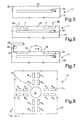
- Figure 2 shows a wafer 11 of semiconductor material, for example monocrystalline silicon, comprising a substrate 12, for example of N type.
- a resist mask 13 is made on the wafer 11 (reference may also be made to the cross-section of Figure 3 ).
- the mask 13 has an approximately square area 14 comprising a plurality of hexagonal mask portions 13a that define a honeycomb lattice (as visible in the enlarged detail of Figure 2 ).
- the distance t between opposite sides of the mask portions 13a is 2 ⁇ m, while the distance d between facing sides of adjacent mask portions 13a is 1 ⁇ m.
- the substrate 12 is anisotropically etched, thereby forming trenches 16, having for example a depth of 10 ⁇ m, which communicate with one another and delimit a plurality of columns 17 of silicon.
- the trenches 16 form an open region 18 of a complex shape (corresponding to the honeycomb lattice of the mask 13) accommodating the columns 17 (with the same as the mask portions 13a).
- an epitaxial growth is performed in a de-oxidizing environment (typically, in an atmosphere with a high concentration of hydrogen, preferably with trichlorosilane - SiHCl 3 ). Consequently, an epitaxial layer 20, for example of an N type and having a thickness of 9 ⁇ m, grows on top of the columns 17 and closes the open region 18 at the top.
- the epitaxial layer 20 is shown only in Figure 5 and thereafter not distinguished from the substrate 12.
- a thermal annealing is then performed, for example for 30 minutes at 1190°C, preferably in a hydrogen atmosphere, or alternatively a nitrogen atmosphere.
- the annealing causes a migration of the silicon atoms, which tend to move into the lower energy position. Consequently, and also thanks to the small distance between the columns 17, the silicon atoms migrate completely from the portions of the columns 17 within the open region 18, and a buried cavity 22 is formed, having a side of for example 500 ⁇ m.
- a thin silicon layer remains on top of the buried cavity 22 and forms a membrane 23, that is formed in part by epitaxially grown silicon atoms and in part by migrated silicon atoms.
- the membrane 23 is flexible and can undergo deflection in presence of external stresses.
- piezoresistive elements 24 are formed in a surface portion of the membrane 23 opposite to the cavity 22.
- the piezoresistive elements 24 are obtained by diffusion or implantation of P type, for example of boron atoms, and are connected to one another in a Wheatstone-bridge configuration, as will be explained in detail hereinafter.
- the interconnections 26 between the piezoresistive elements 24 are represented in a schematic way.
- the piezoresistive elements 24 can be made of polysilicon on top of the membrane 23.
- an inertial mass 25 is deposited, using a silk-screen printing technique, and is formed by welding paste, for example of silver, tin, copper, lead, gold, or of other high-density metals (preferably having a density higher than 7000 kg/m 3 ).
- welding paste for example of silver, tin, copper, lead, gold, or of other high-density metals (preferably having a density higher than 7000 kg/m 3 ).
- the welding paste is commonly used in the fabrication of packages of electronic components.
- the inertial mass 25 is deposited approximately at the geometrical centre of the membrane 23 through a metal mesh (not illustrated), for example of nickel or steel, which has suitable openings at the deposition areas of the welding paste.
- Deposition is accompanied by an increase in temperature, during which the inertial mass 25 adheres to the top surface of the membrane 23.
- the shape of the inertial mass 25 (as illustrated in Figure 7 and in the top plan view of Figure 8 ) comprises a cylindrical base portion and a hemispherical top portion.
- the inertial mass 25 has a height such that its centroid G is located outside of the membrane 23.
- the shape of the inertial mass 25 is given not only by the size of the openings of the metal mesh used for its deposition, but also by the surface tensile stresses created between the inertial mass 25 and the membrane 23, and by the resting base of the inertial mass 25 on the membrane 23.
- a covering region 28, for example of semiconductor material or glass, can possibly be bonded via anodic bonding to the top surface of the wafer 11, for ensuring a mechanical protection for the sensing structure.
- the covering region 28 has a cavity 29 at the membrane 23, so as to not alter the freedom of movement.
- Figure 8 shows a top plan view of the wafer 11, highlighting the arrangement of the piezoresistive elements 24 with respect to the inertial mass 25.
- the axes x, y and z of a Cartesian reference system associated to the wafer 11 are also shown in Figure 8 .
- the top surface of the wafer 11 lies in the plane xy.
- the piezoresistive elements 24 are arranged to form a cross along the axes x and y, and the inertial mass 25 is located at the centre thereof.
- Each arm of the cross is formed by two groups of four piezoresistive elements 24 aligned and connected to one another in a Wheatstone-bridge configuration.
- the piezoresistive elements 24, designated by R 1x -R 4x refer to the detection of an acceleration along the axis x
- the ones designated by R 1y -R 4y refer to the detection of an acceleration along the axis y
- the ones designated by R 1z -R 4z and R 1z '-R 4z ' refer to the detection of an acceleration along the axis z. Consequently there are present a Wheatstone bridge for detecting an acceleration along the axis x and the axis y, and two Wheatstone bridges connected in common mode for detecting an acceleration along the axis z.
- the piezoresistive elements R 1x/ R 1y and R 3x /R 3y undergo a tensile stress, which increases their own resistivity, while the piezoresistive elements R 2x /R 2y and R 4x /R 4y undergo a compressive stress, which decreases their own resistivity.
- the piezoresistive elements 24 referred to above are arranged in a Wheatstone-bridge configuration so as to increase the sensitivity of the bridge, i.e., elements with resistivities which undergo opposite variations are arranged in adjacent arms of the bridge.
- FIG. 10a shows the piezoresistive elements R 1z and R 4z undergo a tensile stress, that increases their own resistivity, while the piezoresistive elements R 2z and R 3z undergo a compressive stress, that decreases their own resistivity.
- Figure 10b shows the corresponding arrangement in a Wheatstone-bridge configuration of the piezoresistive elements 24 mentioned above.
- the buried cavity 22 has a thickness of a few microns, the possibility of deflection of the membrane in the direction of the axis z is limited. In this way, a mechanical constraint is created that limits the amplitude of the displacements along the axis z, to prevent any possible failure of the accelerometer.
- Figure 11 shows the distribution of the stresses acting on the membrane 23 upon application of an acceleration of 5 g along the axis z.
- the intensity of the compressive stress has a maximum value in the neighbourhood of the inertial mass 25 (represented as a spheroid in Figure 11 ), while the intensity of the tensile stress is maximum at the peripheral edges of the membrane 23.
- the piezoresistive elements R 1z -R 4z are consequently formed at the regions of the membrane 23 that are subjected to the stresses of maximum intensity. Similar considerations apply to the piezoresistive elements 24 corresponding to the axes x and y.
- the unbalancing of the Wheatstone bridge is then detected by an appropriate electronic circuit, generally comprising an instrumentation amplifier, which receives the unbalancing voltage V out of the Wheatstone bridge; the desired information of acceleration is then derived from the unbalancing.
- an appropriate electronic circuit generally comprising an instrumentation amplifier, which receives the unbalancing voltage V out of the Wheatstone bridge; the desired information of acceleration is then derived from the unbalancing.
- the sensitivity Sens of the accelerometer is directly affected by the dimensions of the inertial mass 25.
- the sensitivity Sens increases as the inertial mass 25 increases, in so far as the consequent deformation of the membrane 23 increases, but only up to a certain limit, beyond which the dimensions of the inertial mass 25 become such as to stiffen the membrane 23 excessively and to limit its freedom of movement.
- the tables of Figures 12a and 12b illustrate the value of the sensitivity Sens of the accelerometer as the radius of the inertial mass 25 (again shown as a spheroid) varies, respectively for an acceleration acting in the plane xy and for an acceleration acting in the direction z.
- the value of sensitivity is normalized with an acceleration of 5 g and a voltage of 5 V, and is expressed in ⁇ V/g/V.
- the tables give moreover the values, expressed in Pa, of the longitudinal stresses S l and of the transverse stresses S t (corresponding to the position of the piezoresistive elements 24 in the plane xy) to which the membrane 23 is subjected.
- the accelerometer is found to have a higher sensitivity when the ratio between the radius of the inertial mass 25 and the side of the membrane 23 is between 20% and 40% (or, likewise, the ratio between the diameter of the inertial mass 25 and the side of the membrane 23 is between 40% and 80%). Furthermore, it emerges that the sensitivity of the accelerometer is higher along the axis z than along the axes x and y.
- the accelerometer described is used in a device for monitoring the inflation pressure of the tyres of a vehicle.
- a pressure-monitoring device 30 comprises an accelerometer 35, made as described previously and designed to detect the centrifugal acceleration of a tyre (not illustrated); a pressure sensor 36, of piezoresistive type, connected to the accelerometer 35 and designed to measure the pressure of inflation of the tyre; and an electronic circuit 37, connected to the accelerometer 35 and to the pressure sensor 36 and communicating with the electronic control unit of the motor vehicle (not shown), for example via radio-frequencies.
- the pressure-monitoring device 30 is arranged at the inner surface of the tyre, so that the accelerometer 35b detects the centrifugal acceleration along the axis z due to the rotation of the tyre.
- the technology used for manufacturing the accelerometer 35 is substantially similar to the one used for the pressure sensor 36 (see in this regard the aforementioned European patent application No. 04 425 197.3 ). Consequently, integration of the pressure sensor and of the accelerometer according to the present invention in a same substrate of semiconductor material proves simple and economically advantageous. Furthermore, also the electronic circuit 37 can be readily integrated in the same substrate, rendering the pressure-monitoring device 30 extremely compact and simple and fast to produce.
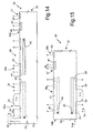
- Figure 14 shows the pressure-monitoring device 30 integrated in a wafer 31 of semiconductor material, for example of monocrystalline silicon, which comprises a substrate 32, for example of an N type.
- a first region 34a accommodating an accelerometer 35 made as described with reference to Figures 2 to 7 (so that parts that are similar are designated by the same reference numbers); a second region 34b, accommodating a piezoresistive pressure sensor 36; and a third region 34c, accommodating an electronic circuit 37.
- the pressure sensor 36 comprises a buried cavity 40, a membrane 41, and piezoresistive elements 42 diffused or implanted within the membrane 41.
- a fair number of the manufacturing process of the pressure sensor 36 and of the accelerometer 35 are in common (for example, forming the trenches, annealing, depositing the piezoresistive elements, etc.).
- the electronic control circuit 37 ( Figure 14 shows only by way of example an NPN transistor comprising a collector region 45 of an N type, a base region 46 of a P type, and an emitter region 47 of an N type) is also made using manufacturing steps in common with the process of the accelerometer 35 and of the pressure sensor 36. For example, the diffusion of the base region 46 is performed simultaneously with the diffusion of the piezoresistive elements. In a way not illustrated in Figure 14 , electrical-insulation regions can be envisaged for insulating electrically the electronic control circuit 37 from the second region 34b.
- the wafer 31 can then be encapsulated in a package 51 (illustrated schematically in Figure 14 ) so that only the membrane 41 of the pressure sensor 36 is accessible from the outside, while the remaining components are mechanically protected.
- the above described pressure-monitoring device has the following advantages.
- the related accelerometer has extremely reduced dimensions, since it is integrated in a single substrate and does not need bonding of wafers of different materials. Furthermore, the fabrication of the inertial mass using welding paste of high-density metals enables, for a same sensitivity, to reduce the dimensions of the inertial mass as compared to when other materials having a lower density (for example silicon) are used.
- the manufacturing process is extremely simple and inexpensive, and furthermore, the particular construction is compatible with packaging techniques at the substrate level, such as the bump-bonding or flip-chip techniques, which enable a further reduction in the dimensions.
- the sensitive part of the sensor is automatically and mechanically protected on the back of the wafer because of the presence of the buried cavity within the substrate.
- the pressure-monitoring device is, in turn, extremely compact, thanks to the integration of all the components, including the electronic control circuit, in a single body of semiconductor material. In this way, it is possible to reach dimensions smaller than 1 mm. Furthermore, the manufacturing process is simpler and faster, since process steps for obtaining the various components of the device are in common. The resulting chip can also be connected with flip-chip techniques.
- a second embodiment of the pressure-monitoring device 30 provides for forming the accelerometer 35 on the back of the wafer 31, so as to obtain a further reduction of the occupied area.
- the manufacturing process according to the second embodiment comprises first forming the pressure sensor 36 in a front surface portion of the wafer 31. Then, after coating the top surface of the wafer 31 with a sheet of protective material, the wafer 31 is turned upside down (this is possible given the planarity of the pressure sensor 36 and the absence of any projecting portions), so as to obtain the accelerometer 35 on the back of the wafer 31.
- the annealing steps can advantageously be made simultaneously for both of the sensors.
- the geometrical shape of the membrane can be different, for example can be circular or generically polygonal; also the shape of the inertial mass can differ from the one described and can be, for example, cylindrical.
- the shape of the columns 17 can vary with respect to the one illustrated; for example the columns 17 can be replaced by diaphragms of semiconductor material of small thickness, or in general by other thin structures (walls) such as to enable migration of silicon during the annealing step and formation of the deep buried cavity 22.
- the described accelerometer can advantageously be used for other applications, in particular in all those applications that require reduced overall dimensions and costs.
- it can be used in a wake-up system of a portable device, or for detection of a free fall of the portable device.
- the described pressure-monitoring device can be used for other applications.
- it can be used for monitoring the pressure of the air-bag, for controlling the breakdown pressure of the ABS, and for monitoring the pressure of the oil or the pressure of fuel injection.
Landscapes
- Physics & Mathematics (AREA)
- General Physics & Mathematics (AREA)
- Pressure Sensors (AREA)
- Measuring Fluid Pressure (AREA)
Abstract
Description
- The present invention relates to a process for manufacturing a pressure-monitoring device provided with a triaxial piezoresistive accelerometer, in particular a device for monitoring the pressure of the tyres of a motor vehicle, to which the ensuing description will make explicit reference, without any loss of generality.
- As known, in the automotive field there is an increasing use of devices for monitoring the pressure of tyres (generally known as tyre-pressure monitoring systems - TPMSs), which are designed to supply a timely communication, to the electronic control unit of the vehicle, of any fault or deviation with respect to the correct values of operation. These monitoring devices generally comprise a pressure sensor installed on the inner surface of the tyre and designed to monitor its state of inflation; an appropriate electronic circuit, which reads the data provided by the pressure sensor and communicates with the electronic control unit (generally using radio-frequencies); and a wake-up system, which supplies a start-of-measurement signal to the pressure sensor and a data-collection signal to the electronic circuit connected thereto. In particular, the wake-up system makes it possible to limit the monitoring operation to the time intervals when the vehicle is moving (it is estimated that the average time of effective use of a vehicle is around 5% of the total life of the vehicle), and thus to reduce the energy consumption by the vehicle battery. Known wake-up systems are either of a mechanical type, generally formed by a mass coupled to a spring, or, as in the case of more recent systems, of an electronic type. Wake-up systems of an electronic type comprise an accelerometer arranged so as to detect the centrifugal acceleration of the tyre as it turns. An acceleration of intensity higher than a preset threshold indicates a movement condition of the vehicle.
- The various components of the device for monitoring pressure are currently made using different technologies and subsequently assembled on an electronic board. The device is then coated with resin and individually packaged. Consequently, the pressure-monitoring device is currently cumbersome (around 10 mm in size) and somewhat complex to produce.
- Recently, the use has been proposed, within the pressure-monitoring device, of semiconductor piezoresistive accelerometers made using microfabrication techniques.
- As is known, piezoresistive sensors base their operation on piezoresistivity, i.e., the capacity of certain materials to modify their resistivity as the mechanical stresses acting on them vary. In detail, the resistivity decreases when compressive stresses are applied, whereas it increases when tensile stresses are applied.
- Semiconductor piezoresistive accelerometers generally comprise a membrane (or diaphragm) suspended over a cavity, and an inertial mass fixed to the membrane, and mobile with one or more degrees of freedom after detecting an acceleration. Piezoresistive elements (generally formed by implanted or diffused regions) are made in the surface region of the membrane and are connected to one another in a Wheatstone-bridge configuration. A deformation of the membrane, caused by the displacement of the inertial mass induced by the acceleration, causes an unbalancing of the Wheatstone bridge, which can be detected by a purposely provided electronic circuit, which derives, from said unbalancing, the desired measurement of acceleration.
- A triaxial piezoresistive accelerometer of a known type is, for example, manufactured by Fujikura Ltd. and described in detail in "www.sensorsmag.com/articles/0299/0299_38/main.shtml".
- This accelerometer is illustrated in
Figure 1 , where it is designated as a whole byreference number 1. Theaccelerometer 1 comprises a first and asecond silicon layer glass layer 4 is arranged. In particular, the layers are bonded to one another via anodic bonding, and the entire structure is enclosed in a ceramic package (not illustrated inFigure 1 ). - In extreme synthesis, the manufacturing process of the
accelerometer 1 envisages the diffusion of boron regions in the surface region of thefirst silicon layer 2 so as to formpiezoresistive elements 6 that are connected in a Wheatstone-bridge configuration (not illustrated inFigure 1 ). Then, the rear face of thefirst silicon layer 1 is anisotropically etched so as to form a thin silicon membrane 8. After the etch, acentral portion 9 of thefirst silicon layer 2 remains underneath the membrane 8. Next, theglass layer 4 is bonded to the rear surface of thefirst silicon layer 2 via anodic bonding and the layer ofglass 4 is cut on the rear side (opposite to the bonding side), so as to form aninertial mass 10 at the centre of the structure of theaccelerometer 1, underneath the membrane 8. In particular, theinertial mass 10 is etched only at thecentral portion 9. Finally, thesecond silicon layer 3 is bonded via anodic bonding underneath the layer ofglass 4, which has the function of base and of mechanical protection for theaccelerometer 1. At theinertial mass 10, thesecond silicon layer 3 has acavity 12, appropriately made before bonding, so as to ensure freedom of movement to theinertial mass 10. The distance between theinertial mass 10 and thesecond silicon layer 3 is such as to limit the movement of theinertial mass 10 in a transverse direction, to prevent the membrane 8 from getting damaged in case of excessive accelerations. - An acceleration imparted upon the
accelerometer 1 causes a displacement of theinertial mass 10, and a consequent deformation of the membrane 8. Due to this deformation, thepiezoresistive elements 6 vary their resistivity, so unbalancing the Wheatstone bridge. - The
accelerometer 1 described, even though it is certainly more compact than wake-up systems of a mechanical type, has in any case large dimensions on account of the need to carry out a bonding of three different layers (two layers of silicon and one layer of glass) and on account of the presence of a ceramic package, and entails a manufacturing process that is somewhat complex and costly. Furthermore, theaccelerometer 1 cannot be readily integrated with the electronic read circuit. These disadvantages are particularly evident as regards the considered automotive applications, wherein low cost and simplicity of production are a constraint in the choice of the components to be used. - The aim of the present invention is to provide a pressure-monitoring device, in particular for automotive applications, overcoming the aforesaid disadvantages and problems, and in particular being simple and inexpensive to manufacture.
- According to the present invention, there are consequently provided a process for manufacturing a pressure-monitoring device as defined in
claim 1, and a pressure-monitoring device as defined inclaim 11. - For a better understanding of the present invention, a preferred embodiment thereof is now described, purely by way of non-limiting example and with reference to the attached plate of drawings, wherein:
-
Figure 1 shows a cross-section of a piezoresistive accelerometer according to a known technique; -
Figure 2 shows a top plan view of a wafer of semiconductor material in an initial step of a process of manufacturing an accelerometer of a pressure-monitoring device according to the present invention; -
Figures 3-7 are cross-sections through the wafer ofFigure 2 in subsequent steps of the manufacturing process according to the present invention; -
Figure 8 shows a top plan view of the wafer ofFigure 7 ; -
Figures 9a-10a are schematic representations of a portion of the wafer ofFigure 7 , when subjected to accelerations; -
Figures 9b-10b show the bridge configuration of piezoresistive elements of the wafer ofFigure 7 ; -
Figure 11 shows a diagram corresponding to the distribution of the strains acting on a membrane portion of the wafer ofFigure 7 when this is subjected to accelerations; -
Figures 12a and 12b are tables of sensitivity values of the accelerometer of the pressure-monitoring device according to the present invention; -
Figure 13 shows a block diagram of a pressure-monitoring device according to the present invention; -
Figure 14 is a cross-section through a wafer of semiconductor material accommodating a pressure-monitoring device according to a first embodiment of the present invention; and -
Figure 15 shows a second embodiment of the pressure-monitoring device ofFigure 14 . - Hereinafter an embodiment is described of a manufacturing process of a triaxial piezoresistive accelerometer of semiconductor material of a pressure-monitoring device. The manufacturing process is based upon the process described in
EP-A-1 324 382 , for manufacturing a SOI wafer, and on the process described in European patent application No.04 425 197.3 -
Figure 2 shows awafer 11 of semiconductor material, for example monocrystalline silicon, comprising asubstrate 12, for example of N type. - In an initial step of the manufacturing process, a
resist mask 13 is made on the wafer 11 (reference may also be made to the cross-section ofFigure 3 ). In detail, themask 13 has an approximatelysquare area 14 comprising a plurality ofhexagonal mask portions 13a that define a honeycomb lattice (as visible in the enlarged detail ofFigure 2 ). For example, the distance t between opposite sides of themask portions 13a is 2 µm, while the distance d between facing sides ofadjacent mask portions 13a is 1 µm. - Next (reference is made to
Figure 4 ), using themask 13, thesubstrate 12 is anisotropically etched, thereby formingtrenches 16, having for example a depth of 10 µm, which communicate with one another and delimit a plurality ofcolumns 17 of silicon. In practice, thetrenches 16 form anopen region 18 of a complex shape (corresponding to the honeycomb lattice of the mask 13) accommodating the columns 17 (with the same as themask portions 13a). - Next (
Figure 5 ), themask 13 is removed and an epitaxial growth is performed in a de-oxidizing environment (typically, in an atmosphere with a high concentration of hydrogen, preferably with trichlorosilane - SiHCl3). Consequently, anepitaxial layer 20, for example of an N type and having a thickness of 9 µm, grows on top of thecolumns 17 and closes theopen region 18 at the top. Theepitaxial layer 20 is shown only inFigure 5 and thereafter not distinguished from thesubstrate 12. - A thermal annealing is then performed, for example for 30 minutes at 1190°C, preferably in a hydrogen atmosphere, or alternatively a nitrogen atmosphere.
- As discussed in the aforementioned patent applications, the annealing causes a migration of the silicon atoms, which tend to move into the lower energy position. Consequently, and also thanks to the small distance between the
columns 17, the silicon atoms migrate completely from the portions of thecolumns 17 within theopen region 18, and a buriedcavity 22 is formed, having a side of for example 500 µm. A thin silicon layer remains on top of the buriedcavity 22 and forms amembrane 23, that is formed in part by epitaxially grown silicon atoms and in part by migrated silicon atoms. Themembrane 23 is flexible and can undergo deflection in presence of external stresses. - Next (
Figure 6 ),piezoresistive elements 24 are formed in a surface portion of themembrane 23 opposite to thecavity 22. In detail, thepiezoresistive elements 24 are obtained by diffusion or implantation of P type, for example of boron atoms, and are connected to one another in a Wheatstone-bridge configuration, as will be explained in detail hereinafter. InFigure 6 , theinterconnections 26 between the piezoresistive elements 24 (typically formed by metal regions extending on an insulating layer, not illustrated) are represented in a schematic way. Furthermore, as an alternative to what is illustrated, thepiezoresistive elements 24 can be made of polysilicon on top of themembrane 23. - Next (
Figure 7 ), on top of themembrane 23 aninertial mass 25 is deposited, using a silk-screen printing technique, and is formed by welding paste, for example of silver, tin, copper, lead, gold, or of other high-density metals (preferably having a density higher than 7000 kg/m3). For example, the welding paste is commonly used in the fabrication of packages of electronic components. - In detail, the
inertial mass 25 is deposited approximately at the geometrical centre of themembrane 23 through a metal mesh (not illustrated), for example of nickel or steel, which has suitable openings at the deposition areas of the welding paste. - Deposition is accompanied by an increase in temperature, during which the
inertial mass 25 adheres to the top surface of themembrane 23. After cooling, the shape of the inertial mass 25 (as illustrated inFigure 7 and in the top plan view ofFigure 8 ) comprises a cylindrical base portion and a hemispherical top portion. In particular, theinertial mass 25 has a height such that its centroid G is located outside of themembrane 23. The shape of theinertial mass 25 is given not only by the size of the openings of the metal mesh used for its deposition, but also by the surface tensile stresses created between theinertial mass 25 and themembrane 23, and by the resting base of theinertial mass 25 on themembrane 23. - Next, a
covering region 28, for example of semiconductor material or glass, can possibly be bonded via anodic bonding to the top surface of thewafer 11, for ensuring a mechanical protection for the sensing structure. In particular, thecovering region 28 has acavity 29 at themembrane 23, so as to not alter the freedom of movement. -
Figure 8 shows a top plan view of thewafer 11, highlighting the arrangement of thepiezoresistive elements 24 with respect to theinertial mass 25. The axes x, y and z of a Cartesian reference system associated to thewafer 11 are also shown inFigure 8 . In particular, the top surface of thewafer 11 lies in the plane xy. - In detail, the
piezoresistive elements 24 are arranged to form a cross along the axes x and y, and theinertial mass 25 is located at the centre thereof. Each arm of the cross is formed by two groups of fourpiezoresistive elements 24 aligned and connected to one another in a Wheatstone-bridge configuration. As will be described in detail hereinafter, thepiezoresistive elements 24, designated by R1x-R4x, refer to the detection of an acceleration along the axis x, the ones designated by R1y-R4y refer to the detection of an acceleration along the axis y, and the ones designated by R1z-R4z and R1z'-R4z' refer to the detection of an acceleration along the axis z. Consequently there are present a Wheatstone bridge for detecting an acceleration along the axis x and the axis y, and two Wheatstone bridges connected in common mode for detecting an acceleration along the axis z. - Operation of the above triaxial accelerometer is described hereinafter (see
Figures 9 and 10 ). - Since the centroid G of the
inertial mass 25 is located outside of themembrane 23, an acceleration directed along the axis x or the axis y acting on the accelerometer brings about a momentum on theinertial mass 25, which causes inclination thereof in the corresponding direction (as illustrated inFigure 9a ). The displacement of theinertial mass 25 brings about a corresponding deformation of themembrane 23 and a variation in the resistivity of thepiezoresistive elements 24 arranged along the direction of the acceleration. In particular, the piezoresistive elements R1x/R1y and R3x/R3y undergo a tensile stress, which increases their own resistivity, while the piezoresistive elements R2x/R2y and R4x/R4y undergo a compressive stress, which decreases their own resistivity. As illustrated inFigure 9b , thepiezoresistive elements 24 referred to above are arranged in a Wheatstone-bridge configuration so as to increase the sensitivity of the bridge, i.e., elements with resistivities which undergo opposite variations are arranged in adjacent arms of the bridge. - Likewise, an acceleration directed along the axis z acting on the accelerometer causes a corresponding displacement of the
inertial mass 25 and a consequent deformation of themembrane 23, as illustrated inFigure 10a . In this case, the piezoresistive elements R1z and R4z undergo a tensile stress, that increases their own resistivity, while the piezoresistive elements R2z and R3z undergo a compressive stress, that decreases their own resistivity.Figure 10b shows the corresponding arrangement in a Wheatstone-bridge configuration of thepiezoresistive elements 24 mentioned above. - It should be noted that, since the buried
cavity 22 has a thickness of a few microns, the possibility of deflection of the membrane in the direction of the axis z is limited. In this way, a mechanical constraint is created that limits the amplitude of the displacements along the axis z, to prevent any possible failure of the accelerometer. -
Figure 11 shows the distribution of the stresses acting on themembrane 23 upon application of an acceleration of 5 g along the axis z. As may be noted, the intensity of the compressive stress has a maximum value in the neighbourhood of the inertial mass 25 (represented as a spheroid inFigure 11 ), while the intensity of the tensile stress is maximum at the peripheral edges of themembrane 23. The piezoresistive elements R1z-R4z are consequently formed at the regions of themembrane 23 that are subjected to the stresses of maximum intensity. Similar considerations apply to thepiezoresistive elements 24 corresponding to the axes x and y. - In a per se known and not illustrated manner, the unbalancing of the Wheatstone bridge is then detected by an appropriate electronic circuit, generally comprising an instrumentation amplifier, which receives the unbalancing voltage Vout of the Wheatstone bridge; the desired information of acceleration is then derived from the unbalancing.
- The sensitivity Sens of the accelerometer is directly affected by the dimensions of the
inertial mass 25. In particular, the sensitivity Sens increases as theinertial mass 25 increases, in so far as the consequent deformation of themembrane 23 increases, but only up to a certain limit, beyond which the dimensions of theinertial mass 25 become such as to stiffen themembrane 23 excessively and to limit its freedom of movement. - The tables of
Figures 12a and 12b illustrate the value of the sensitivity Sens of the accelerometer as the radius of the inertial mass 25 (again shown as a spheroid) varies, respectively for an acceleration acting in the plane xy and for an acceleration acting in the direction z. The value of sensitivity is normalized with an acceleration of 5 g and a voltage of 5 V, and is expressed in µV/g/V. The tables give moreover the values, expressed in Pa, of the longitudinal stresses S l and of the transverse stresses S t (corresponding to the position of thepiezoresistive elements 24 in the plane xy) to which themembrane 23 is subjected. - From the tests conducted by the applicant, it emerges that, in order to obtain a higher sensitivity Sens of the accelerometer, it is convenient to use
inertial masses 25 having a radius of between 100 µm and 200 µm. With reference to the dimensions of the membrane 23 (the side whereof is approximately 500 µm), the accelerometer is found to have a higher sensitivity when the ratio between the radius of theinertial mass 25 and the side of themembrane 23 is between 20% and 40% (or, likewise, the ratio between the diameter of theinertial mass 25 and the side of themembrane 23 is between 40% and 80%). Furthermore, it emerges that the sensitivity of the accelerometer is higher along the axis z than along the axes x and y. - The accelerometer described is used in a device for monitoring the inflation pressure of the tyres of a vehicle.
- In detail, as illustrated in
Figure 13 , a pressure-monitoringdevice 30 comprises anaccelerometer 35, made as described previously and designed to detect the centrifugal acceleration of a tyre (not illustrated); apressure sensor 36, of piezoresistive type, connected to theaccelerometer 35 and designed to measure the pressure of inflation of the tyre; and anelectronic circuit 37, connected to theaccelerometer 35 and to thepressure sensor 36 and communicating with the electronic control unit of the motor vehicle (not shown), for example via radio-frequencies. In particular, the pressure-monitoringdevice 30 is arranged at the inner surface of the tyre, so that the accelerometer 35b detects the centrifugal acceleration along the axis z due to the rotation of the tyre. - The technology used for manufacturing the
accelerometer 35 is substantially similar to the one used for the pressure sensor 36 (see in this regard the aforementioned European patent application No.04 425 197.3 electronic circuit 37 can be readily integrated in the same substrate, rendering the pressure-monitoringdevice 30 extremely compact and simple and fast to produce. -
Figure 14 shows the pressure-monitoringdevice 30 integrated in awafer 31 of semiconductor material, for example of monocrystalline silicon, which comprises asubstrate 32, for example of an N type. - Within the
wafer 31 three regions may be distinguished: afirst region 34a, accommodating anaccelerometer 35 made as described with reference toFigures 2 to 7 (so that parts that are similar are designated by the same reference numbers); asecond region 34b, accommodating apiezoresistive pressure sensor 36; and athird region 34c, accommodating anelectronic circuit 37. - In detail, the
pressure sensor 36 comprises a buriedcavity 40, amembrane 41, andpiezoresistive elements 42 diffused or implanted within themembrane 41. Advantageously, a fair number of the manufacturing process of thepressure sensor 36 and of theaccelerometer 35 are in common (for example, forming the trenches, annealing, depositing the piezoresistive elements, etc.). - The electronic control circuit 37 (
Figure 14 shows only by way of example an NPN transistor comprising acollector region 45 of an N type, abase region 46 of a P type, and anemitter region 47 of an N type) is also made using manufacturing steps in common with the process of theaccelerometer 35 and of thepressure sensor 36. For example, the diffusion of thebase region 46 is performed simultaneously with the diffusion of the piezoresistive elements. In a way not illustrated inFigure 14 , electrical-insulation regions can be envisaged for insulating electrically theelectronic control circuit 37 from thesecond region 34b. - At the end of the manufacturing process, after depositing the
inertial mass 25 of theaccelerometer 35, appropriate electrical-contact regions 50 (illustrated schematically) are made for the electrical connection of theaccelerometer 35, of thepressure sensor 36, and of theelectronic control circuit 37. Further electrical-contact regions are provided for the electrical connection of theelectronic circuit 37 with the outside world (in particular with the electronic control unit of the vehicle, not illustrated herein). - The
wafer 31 can then be encapsulated in a package 51 (illustrated schematically inFigure 14 ) so that only themembrane 41 of thepressure sensor 36 is accessible from the outside, while the remaining components are mechanically protected. - The above described pressure-monitoring device has the following advantages.
- In particular, the related accelerometer has extremely reduced dimensions, since it is integrated in a single substrate and does not need bonding of wafers of different materials. Furthermore, the fabrication of the inertial mass using welding paste of high-density metals enables, for a same sensitivity, to reduce the dimensions of the inertial mass as compared to when other materials having a lower density (for example silicon) are used. The manufacturing process is extremely simple and inexpensive, and furthermore, the particular construction is compatible with packaging techniques at the substrate level, such as the bump-bonding or flip-chip techniques, which enable a further reduction in the dimensions. Furthermore, the sensitive part of the sensor is automatically and mechanically protected on the back of the wafer because of the presence of the buried cavity within the substrate.
- The pressure-monitoring device is, in turn, extremely compact, thanks to the integration of all the components, including the electronic control circuit, in a single body of semiconductor material. In this way, it is possible to reach dimensions smaller than 1 mm. Furthermore, the manufacturing process is simpler and faster, since process steps for obtaining the various components of the device are in common. The resulting chip can also be connected with flip-chip techniques.
- Finally, it is clear that modifications and variations can be made to the process and device described and illustrated herein, without thereby departing from the scope of the present invention, as defined in the annexed claims.
- In particular (see
Figure 15 ), a second embodiment of the pressure-monitoringdevice 30 provides for forming theaccelerometer 35 on the back of thewafer 31, so as to obtain a further reduction of the occupied area. In detail, the manufacturing process according to the second embodiment comprises first forming thepressure sensor 36 in a front surface portion of thewafer 31. Then, after coating the top surface of thewafer 31 with a sheet of protective material, thewafer 31 is turned upside down (this is possible given the planarity of thepressure sensor 36 and the absence of any projecting portions), so as to obtain theaccelerometer 35 on the back of thewafer 31. In particular, the annealing steps can advantageously be made simultaneously for both of the sensors. - In addition, the geometrical shape of the membrane can be different, for example can be circular or generically polygonal; also the shape of the inertial mass can differ from the one described and can be, for example, cylindrical.
- The shape of the
columns 17 can vary with respect to the one illustrated; for example thecolumns 17 can be replaced by diaphragms of semiconductor material of small thickness, or in general by other thin structures (walls) such as to enable migration of silicon during the annealing step and formation of the deep buriedcavity 22. - Furthermore, it is clear that the described accelerometer can advantageously be used for other applications, in particular in all those applications that require reduced overall dimensions and costs. For example, it can be used in a wake-up system of a portable device, or for detection of a free fall of the portable device.
- Finally, the described pressure-monitoring device can be used for other applications. For example, in the automotive field, it can be used for monitoring the pressure of the air-bag, for controlling the breakdown pressure of the ABS, and for monitoring the pressure of the oil or the pressure of fuel injection.
Claims (18)
- A process for manufacturing a semiconductor pressure-monitoring device (30), characterized by comprising the steps of:- providing a wafer (31) of semiconductor material;- providing, in a first region (34a) of said wafer (31) a first buried cavity (22) and a first membrane (23), suspended over, and closing at the top, said first buried cavity (22);- providing, in a second region (34b) of said wafer (31), a second buried cavity (40) and a second membrane (41), suspended over, and closing at the top, said second buried cavity (40);- coupling an inertial mass (25) in a rigid way to said first membrane (23), by forming said inertial mass (25) on top of a surface of said first membrane (23) opposite to said first buried cavity (22);- providing, in said first membrane (23), first piezoresistive transduction elements (24) sensitive to strains of said first membrane (23) due to movements of said inertial mass (25) in response to a sensed acceleration and generating corresponding first electrical signals, so as to provide an acceleration sensor (35); and- providing, in said second membrane (41), second piezoresistive transduction elements (42) sensitive to strains of said second membrane (41) in response to a sensed pressure and generating corresponding second electrical signals, so as to provide a pressure sensor (36) integrated with said acceleration sensor (35) in said wafer (31).
- The process according to claim 1, wherein said steps of forming a first (22) and a second (40) buried cavity comprise:- digging, in said first (34a) and, respectively, second (34b) regions of said wafer (31), trenches (16) delimiting between them walls (17) of semiconductor material;- epitaxially growing, starting from said walls (17), a closing layer (20) of semiconductor material, said closing layer (20) closing said trenches (16) at the top; and- carrying out a thermal treatment such as to cause migration of the semiconductor material of said walls (17) and form said first buried cavity (22) and concurrently said first membrane (23) in said first region (34a), and said second buried cavity (40) and concurrently said second membrane (41) in said second region (34b).
- The process according to claim 1 or 2, further comprising the steps of: forming, in a third region (34c) of said wafer (31), an electronic circuit (37), so as to be integrated with said acceleration sensor (35) and pressure sensor (36) in said wafer (31); and forming electrical connection regions (50) for electrical connection of said acceleration sensor (35), pressure sensor (36) and electronic circuit (37).
- The process according to claim 3, wherein said semiconductor pressure-monitoring device (30) is operable for monitoring the pressure of inflation of a tyre of a motor vehicle; said pressure sensor (36) operable for measuring a pressure of inflation of said tyre, and said accelerometer (35) for measuring a centrifugal acceleration caused by rotations of said tyre.
- The process according to claim 3 or 4, wherein said steps of providing said first (24) and second (42) piezoresistive transduction elements and at least part of said step of forming said electronic circuit (37) are carried out substantially at a same time.
- The process according to any of the preceding claims, wherein at least part of said steps of providing said first (22) and second (40) buried cavities are carried out substantially at a same time.
- The process according to any of the preceding claims, wherein said first region (34a) and said second region (34b) are arranged in a same first surface portion of said wafer (31).
- The process according to any of claims 1-6, wherein said first region (34a) is arranged in a first surface portion of said wafer (31) and said second region (34b) is arranged in a second surface portion of said wafer (31), opposite to said first surface portion.
- The process according to any one of the preceding claims, wherein said steps of providing first (24) and second (42) piezoresistive transduction elements comprise providing first (24) and second (42) piezoresistors in a surface portion of said first (23) and second (41) membrane, respectively; said first and second membranes having a first conductivity type and said step of providing first and second piezoresistors comprising introducing ionic dopant species of a second conductivity type.
- The process according to any one of the preceding claims, further comprising the step of coupling a package (51) to said wafer (31), said package (51) being configured to encapsulate said wafer (31) so that only said second membrane (41) of said pressure sensor (36) is accessible from the outside.
- A semiconductor pressure-monitoring device (30), characterized by comprising:- a body (31) of semiconductor material;- a first buried cavity (22) and a first membrane (23) arranged in a first region (34a) of said body (31), said first membrane (23) suspended over, and closing at the top, said first buried cavity (22);- a second buried cavity (40) and a second membrane (41) arranged in a second region (34b) of said body (31), said second membrane (41) suspended over, and closing at the top, said second buried cavity (40);- an inertial mass (25), fixedly coupled to said first membrane (23) and arranged on top a surface of said first membrane (23) opposite to said first buried cavity (22);- first piezoresistive transduction elements (24) arranged in said first membrane (23), sensitive to strains of said first membrane (23) due to movements of said inertial mass (25) in response to a sensed acceleration and generating corresponding first electrical signals, so as to provide an acceleration sensor (35); and- second piezoresistive transduction elements (42) arranged in said second membrane (41), sensitive to strains of said second membrane (41) in response to a sensed pressure and generating corresponding second electrical signals, so as to provide a pressure sensor (36) integrated with said acceleration sensor (35) in said body (31).
- The device according to claim 11, further comprising: an electronic circuit (37), arranged in a third region (34c) of said body (31), so as to be integrated with said acceleration sensor (35) and pressure sensor (36) in said body (31); and electrical connection regions (50) for electrical connection of said acceleration sensor (35), pressure sensor (36) and electronic circuit (37).
- The device according to claim 12, operable for monitoring the pressure of inflation of a tyre of a vehicle; said pressure sensor (36) configured to measure a pressure of inflation of said tyre, and said accelerometer (35) configured to measure a centrifugal acceleration caused by rotations of said tyre.
- The device according to any of the preceding claims 11-13, wherein said first region (34a) and said second region (34b) are arranged in a same first surface portion of said body (31).
- The device according to any of the preceding claims 11-13, wherein said first region (34a) is arranged in a first surface portion of said body (31) and said second region (34b) is arranged in a second surface portion of said body (31), opposite to said first surface portion.
- The device according to any of the preceding claims 11-15, wherein said acceleration sensor (35) is a triaxial accelerometer.
- The device according to any of the preceding claims 11-16, further comprising a package (51) coupled to said body (31), configured to encapsulate said body (31) so that only said second membrane (41) of said pressure sensor (36) is accessible from the outside.
- A tyre-pressure monitoring system for a motor vehicle, comprising the semiconductor pressure-monitoring device (30) as claimed in any of the preceding claims 11-17, wherein said semiconductor pressure-monitoring device (30) is installed on an inner surface of a tyre of said motor vehicle so that said pressure sensor (36) is adapted to measure a pressure of inflation of said tyre, and said accelerometer (35) is adapted to measure a centrifugal acceleration caused by rotations of said tyre; further comprising an electronic control unit operatively coupled to said semiconductor pressure-monitoring device (30).
Priority Applications (1)
| Application Number | Priority Date | Filing Date | Title |
|---|---|---|---|
| EP09161586.4A EP2096448B1 (en) | 2005-01-25 | 2005-01-25 | Process for manufacturing a pressure-monitoring device provided with a triaxial piezoresistive accelerometer |
Applications Claiming Priority (2)
| Application Number | Priority Date | Filing Date | Title |
|---|---|---|---|
| EP09161586.4A EP2096448B1 (en) | 2005-01-25 | 2005-01-25 | Process for manufacturing a pressure-monitoring device provided with a triaxial piezoresistive accelerometer |
| EP05425028A EP1684079A1 (en) | 2005-01-25 | 2005-01-25 | Piezoresistive accelerometer with mass on membrane, and manufacturing process |
Related Parent Applications (2)
| Application Number | Title | Priority Date | Filing Date |
|---|---|---|---|
| EP05425028.7 Division | 2005-01-25 | ||
| EP05425028A Division EP1684079A1 (en) | 2005-01-25 | 2005-01-25 | Piezoresistive accelerometer with mass on membrane, and manufacturing process |
Publications (3)
| Publication Number | Publication Date |
|---|---|
| EP2096448A2 true EP2096448A2 (en) | 2009-09-02 |
| EP2096448A3 EP2096448A3 (en) | 2012-04-04 |
| EP2096448B1 EP2096448B1 (en) | 2016-01-20 |
Family
ID=34943022
Family Applications (2)
| Application Number | Title | Priority Date | Filing Date |
|---|---|---|---|
| EP09161586.4A Expired - Lifetime EP2096448B1 (en) | 2005-01-25 | 2005-01-25 | Process for manufacturing a pressure-monitoring device provided with a triaxial piezoresistive accelerometer |
| EP05425028A Ceased EP1684079A1 (en) | 2005-01-25 | 2005-01-25 | Piezoresistive accelerometer with mass on membrane, and manufacturing process |
Family Applications After (1)
| Application Number | Title | Priority Date | Filing Date |
|---|---|---|---|
| EP05425028A Ceased EP1684079A1 (en) | 2005-01-25 | 2005-01-25 | Piezoresistive accelerometer with mass on membrane, and manufacturing process |
Country Status (2)
| Country | Link |
|---|---|
| US (1) | US7322236B2 (en) |
| EP (2) | EP2096448B1 (en) |
Cited By (5)
| Publication number | Priority date | Publication date | Assignee | Title |
|---|---|---|---|---|
| WO2012122878A1 (en) * | 2011-03-15 | 2012-09-20 | 迈尔森电子(天津)有限公司 | Integrated inertial sensor and pressure sensor, and forming method therefor |
| CN106744649A (en) * | 2015-11-19 | 2017-05-31 | 意法半导体股份有限公司 | Micro electro mechanical device and its manufacture method with two buried cavities |
| US10676347B2 (en) | 2018-01-09 | 2020-06-09 | Stmicroelectronics S.R.L. | Micro-electro-mechanical device having two buried cavities and manufacturing process thereof |
| US11560886B2 (en) | 2019-04-15 | 2023-01-24 | Stmicroelectronics S.R.L. | Micropump MEMS device for moving or ejecting a fluid, in particular microblower or flowmeter |
| US11865581B2 (en) | 2018-11-21 | 2024-01-09 | Stmicroelectronics S.R.L. | Ultrasonic MEMS acoustic transducer with reduced stress sensitivity and manufacturing process thereof |
Families Citing this family (28)
| Publication number | Priority date | Publication date | Assignee | Title |
|---|---|---|---|---|
| DE102005032635A1 (en) * | 2005-07-13 | 2007-01-25 | Robert Bosch Gmbh | Micromechanical device with two sensor structures, method for producing a micromechanical device |
| JP5174673B2 (en) | 2005-10-14 | 2013-04-03 | エスティーマイクロエレクトロニクス エス.アール.エル. | Electronic device with substrate level assembly and method of manufacturing the same |
| US7623414B2 (en) * | 2006-02-22 | 2009-11-24 | Westerngeco L.L.C. | Particle motion vector measurement in a towed, marine seismic cable |
| NL2000835C2 (en) * | 2007-08-29 | 2009-03-03 | Xsens Technologies Bv | Device and method for measuring the dynamic interaction between bodies. |
| DE102008040597A1 (en) * | 2008-07-22 | 2010-01-28 | Robert Bosch Gmbh | Micromechanical component with back volume |
| US8742912B2 (en) * | 2008-12-31 | 2014-06-03 | Stmicroelectronics, Inc. | Self-powered sensor system for monitoring tire pressure |
| US8220330B2 (en) * | 2009-03-24 | 2012-07-17 | Freescale Semiconductor, Inc. | Vertically integrated MEMS sensor device with multi-stimulus sensing |
| EP2252077B1 (en) | 2009-05-11 | 2012-07-11 | STMicroelectronics Srl | Assembly of a capacitive acoustic transducer of the microelectromechanical type and package thereof |
| US8393222B2 (en) | 2010-02-27 | 2013-03-12 | Codman Neuro Sciences Sárl | Apparatus and method for minimizing drift of a piezo-resistive pressure sensor due to progressive release of mechanical stress over time |
| EP2693182A1 (en) * | 2012-07-31 | 2014-02-05 | Honeywell International Inc. | On-chip resonant gyro and pressure sensor |
| US9580302B2 (en) | 2013-03-15 | 2017-02-28 | Versana Micro Inc. | Cell phone having a monolithically integrated multi-sensor device on a semiconductor substrate and method therefor |
| CN104058361A (en) * | 2013-03-20 | 2014-09-24 | 北京大学 | Processing method of integrated piezoresistive accelerometer and pressure meter which are based on prefabricated cavity SOI (silicon on insulator) substrate |
| JP6339669B2 (en) | 2013-07-08 | 2018-06-06 | モーション・エンジン・インコーポレーテッド | MEMS device and method of manufacturing |
| US10273147B2 (en) | 2013-07-08 | 2019-04-30 | Motion Engine Inc. | MEMS components and method of wafer-level manufacturing thereof |
| CN104297520A (en) * | 2013-07-15 | 2015-01-21 | 苏州美仑凯力电子有限公司 | Monolithic embedded integrated silicon acceleration and pressure composite sensor |
| WO2015013828A1 (en) | 2013-08-02 | 2015-02-05 | Motion Engine Inc. | Mems motion sensor and method of manufacturing |
| WO2015103688A1 (en) | 2014-01-09 | 2015-07-16 | Motion Engine Inc. | Integrated mems system |
| US20150247879A1 (en) * | 2014-03-03 | 2015-09-03 | Infineon Technologies Ag | Acceleration sensor |
| US20170030788A1 (en) | 2014-04-10 | 2017-02-02 | Motion Engine Inc. | Mems pressure sensor |
| WO2015184531A1 (en) | 2014-06-02 | 2015-12-10 | Motion Engine Inc. | Multi-mass mems motion sensor |
| EP3153833B1 (en) * | 2014-06-09 | 2020-10-21 | Hitachi Automotive Systems, Ltd. | Dynamic quantity measuring device and pressure sensor using same |
| WO2016090467A1 (en) | 2014-12-09 | 2016-06-16 | Motion Engine Inc. | 3d mems magnetometer and associated methods |
| CA3220839A1 (en) | 2015-01-15 | 2016-07-21 | Motion Engine Inc. | 3d mems device with hermetic cavity |
| ITUB20159497A1 (en) * | 2015-12-24 | 2017-06-24 | St Microelectronics Srl | PIEZOELECTRIC MEMS DEVICE AND ITS MANUFACTURING PROCEDURE |
| IT201700103489A1 (en) | 2017-09-15 | 2019-03-15 | St Microelectronics Srl | METHOD OF MANUFACTURE OF A THIN FILTERING MEMBRANE, ACOUSTIC TRANSDUCER INCLUDING THE FILTERING MEMBRANE, ASSEMBLY METHOD OF THE ACOUSTIC TRANSDUCER AND ELECTRONIC SYSTEM |
| CN108645559A (en) * | 2018-04-13 | 2018-10-12 | 北京协同创新研究院 | A kind of Monolithic integrated MEMS pressure sensor and preparation method thereof |
| US11924983B2 (en) | 2022-03-18 | 2024-03-05 | Honeywell Federal Manufacturing & Technologies, Llc | Electronics module with raceway and submodules |
| CN116621112B (en) * | 2023-05-04 | 2026-01-23 | 中国科学院上海微系统与信息技术研究所 | Manufacturing method of MEMS four-in-one monolithic integrated sensor |
Citations (1)
| Publication number | Priority date | Publication date | Assignee | Title |
|---|---|---|---|---|
| EP1324382A1 (en) | 2001-12-28 | 2003-07-02 | STMicroelectronics S.r.l. | Process for manufacturing an SOI wafer by annealing and oxidation of buried channels |
Family Cites Families (13)
| Publication number | Priority date | Publication date | Assignee | Title |
|---|---|---|---|---|
| US4844970A (en) | 1988-01-12 | 1989-07-04 | Air Products And Chemicals, Inc. | Zirconium (III) salts as cure co-catalysts for nonwoven binders comprising acrylamidoglycolic acid |
| CN1027011C (en) * | 1990-07-12 | 1994-12-14 | 涂相征 | Silicon beam piezoresistive acceleration sensor and manufacturing method thereof |
| JP2776142B2 (en) * | 1992-05-15 | 1998-07-16 | 株式会社日立製作所 | Acceleration sensor |
| US5563344A (en) * | 1992-10-28 | 1996-10-08 | California Institute Of Technology | Dual element electron tunneling accelerometer |
| US5427975A (en) * | 1993-05-10 | 1995-06-27 | Delco Electronics Corporation | Method of micromachining an integrated sensor on the surface of a silicon wafer |
| US5905044A (en) * | 1993-10-09 | 1999-05-18 | Kyungpook National University Technology Research Center | Mass manufacturing method of semiconductor acceleration and vibration sensors |
| US6293154B1 (en) * | 1999-12-10 | 2001-09-25 | Kulite Semiconductor Products | Vibration compensated pressure sensing assembly |
| US6581465B1 (en) * | 2001-03-14 | 2003-06-24 | The United States Of America As Represented By The Secretary Of The Navy | Micro-electro-mechanical systems ultra-sensitive accelerometer |
| US6763718B1 (en) * | 2001-06-26 | 2004-07-20 | The United States Of America As Represented By The Secretary Of The Navy | Micro-electro-mechanical systems ultra-sensitive accelerometer with independent sensitivity adjustment |
| DE10114036A1 (en) * | 2001-03-22 | 2002-10-02 | Bosch Gmbh Robert | Process for the production of micromechanical sensors and sensors produced therewith |
| US6853315B2 (en) * | 2002-01-23 | 2005-02-08 | Triad Sensors, Inc. | Piezoelectric rate sensor system and method |
| DE10250358B4 (en) * | 2002-10-29 | 2017-02-09 | Infineon Technologies Ag | Sensor module for measuring mechanical forces |
| GB0302271D0 (en) * | 2003-01-31 | 2003-03-05 | Melexis Nv | Integrated pressure and acceleration measurement device and a method of manufacture thereof |
-
2005
- 2005-01-25 EP EP09161586.4A patent/EP2096448B1/en not_active Expired - Lifetime
- 2005-01-25 EP EP05425028A patent/EP1684079A1/en not_active Ceased
-
2006
- 2006-01-24 US US11/338,614 patent/US7322236B2/en not_active Expired - Lifetime
Patent Citations (1)
| Publication number | Priority date | Publication date | Assignee | Title |
|---|---|---|---|---|
| EP1324382A1 (en) | 2001-12-28 | 2003-07-02 | STMicroelectronics S.r.l. | Process for manufacturing an SOI wafer by annealing and oxidation of buried channels |
Cited By (10)
| Publication number | Priority date | Publication date | Assignee | Title |
|---|---|---|---|---|
| WO2012122878A1 (en) * | 2011-03-15 | 2012-09-20 | 迈尔森电子(天津)有限公司 | Integrated inertial sensor and pressure sensor, and forming method therefor |
| US9448251B2 (en) | 2011-03-15 | 2016-09-20 | Memsen Electronics Inc | Integrated inertial sensor and pressure sensor, and forming method therefor |
| CN106744649A (en) * | 2015-11-19 | 2017-05-31 | 意法半导体股份有限公司 | Micro electro mechanical device and its manufacture method with two buried cavities |
| US10150666B2 (en) | 2015-11-19 | 2018-12-11 | Stmicroelectronics S.R.L. | Micro-electro-mechanical device and manufacturing process thereof |
| CN106744649B (en) * | 2015-11-19 | 2020-02-14 | 意法半导体股份有限公司 | Microelectromechanical device with two buried cavities and method of manufacturing the same |
| US10626008B2 (en) | 2015-11-19 | 2020-04-21 | Stmicroelectronics S.R.L. | Micro-electro-mechanical device and manufacturing process thereof |
| US10676347B2 (en) | 2018-01-09 | 2020-06-09 | Stmicroelectronics S.R.L. | Micro-electro-mechanical device having two buried cavities and manufacturing process thereof |
| US11358862B2 (en) | 2018-01-09 | 2022-06-14 | Stmicroelectronics S.R.L. | Micro-electro-mechanical device having two buried cavities and manufacturing process thereof |
| US11865581B2 (en) | 2018-11-21 | 2024-01-09 | Stmicroelectronics S.R.L. | Ultrasonic MEMS acoustic transducer with reduced stress sensitivity and manufacturing process thereof |
| US11560886B2 (en) | 2019-04-15 | 2023-01-24 | Stmicroelectronics S.R.L. | Micropump MEMS device for moving or ejecting a fluid, in particular microblower or flowmeter |
Also Published As
| Publication number | Publication date |
|---|---|
| US7322236B2 (en) | 2008-01-29 |
| EP1684079A9 (en) | 2006-10-25 |
| US20060185428A1 (en) | 2006-08-24 |
| EP2096448B1 (en) | 2016-01-20 |
| EP1684079A1 (en) | 2006-07-26 |
| EP2096448A3 (en) | 2012-04-04 |
Similar Documents
| Publication | Publication Date | Title |
|---|---|---|
| EP2096448B1 (en) | Process for manufacturing a pressure-monitoring device provided with a triaxial piezoresistive accelerometer | |
| US7223624B2 (en) | Micromechanical device with thinned cantilever structure and related methods | |
| EP2339357B1 (en) | Method for fabricating a sensor | |
| EP0401635B1 (en) | Manufacturing method of a detector using resistance elements | |
| USRE46671E1 (en) | Substrate-level assembly for an integrated device, manufacturing process thereof and related integrated device | |
| EP3225586B1 (en) | Process for manufacturing a mems pressure sensor, and corresponding mems pressure sensor | |
| US5221400A (en) | Method of making a microaccelerometer having low stress bonds and means for preventing excessive z-axis deflection | |
| EP2517026B1 (en) | Cmos compatible pressure sensor for low pressures | |
| EP3511688B1 (en) | Microelectromechanical piezoresistive pressure sensor with self-test capability and corresponding manufacturing process | |
| CA2232409C (en) | Microelectromechanical accelerometer for automotive applications | |
| EP1775259A1 (en) | Wafer level package for sensor devices | |
| KR100508198B1 (en) | Acceleration sensor | |
| JP2006177823A (en) | Acceleration sensor | |
| US20060261424A1 (en) | Integrated pressure and acceleration measurement device and a method of manufacture thereof | |
| US7678599B2 (en) | Process for the fabrication of an inertial sensor with failure threshold | |
| JPH0484725A (en) | Sensor using resistor element | |
| WO1992015018A1 (en) | Piezoresistive accelerometer and method of fabrication | |
| WO2014011167A1 (en) | Semiconductor secured to substrate via hole in substrate | |
| WO2009114825A2 (en) | Permeable diaphragm piezoresistive based sensors | |
| JP3054938B2 (en) | Semiconductor acceleration sensor | |
| US20250002332A1 (en) | Microelectromechanical sensor device with wafer-level integration of pressure and inertial detection structures and corresponding manufacturing process | |
| JP5401820B2 (en) | Sensor | |
| CN121113183A (en) | A piezoresistive composite sensor and its fabrication method | |
| Dell’Acqua | Sensors: a great chance for microelectronic technologies | |
| JPH04323566A (en) | Semiconductor acceleration sensor |
Legal Events
| Date | Code | Title | Description |
|---|---|---|---|
| PUAI | Public reference made under article 153(3) epc to a published international application that has entered the european phase |
Free format text: ORIGINAL CODE: 0009012 |
|
| AC | Divisional application: reference to earlier application |
Ref document number: 1684079 Country of ref document: EP Kind code of ref document: P |
|
| AK | Designated contracting states |
Kind code of ref document: A2 Designated state(s): DE FR GB IT |
|
| RAP1 | Party data changed (applicant data changed or rights of an application transferred) |
Owner name: STMICROELECTRONICS SRL |
|
| RIC1 | Information provided on ipc code assigned before grant |
Ipc: G01P 15/18 20060101ALI20111104BHEP Ipc: G01P 15/12 20060101AFI20111104BHEP Ipc: G01P 15/08 20060101ALI20111104BHEP |
|
| PUAL | Search report despatched |
Free format text: ORIGINAL CODE: 0009013 |
|
| AK | Designated contracting states |
Kind code of ref document: A3 Designated state(s): DE FR GB IT |
|
| RIC1 | Information provided on ipc code assigned before grant |
Ipc: G01P 15/08 20060101ALI20120228BHEP Ipc: G01P 15/12 20060101AFI20120228BHEP Ipc: G01P 15/18 20060101ALI20120228BHEP |
|
| RAP1 | Party data changed (applicant data changed or rights of an application transferred) |
Owner name: STMICROELECTRONICS SRL |
|
| 17P | Request for examination filed |
Effective date: 20121003 |
|
| 17Q | First examination report despatched |
Effective date: 20130703 |
|
| GRAP | Despatch of communication of intention to grant a patent |
Free format text: ORIGINAL CODE: EPIDOSNIGR1 |
|
| INTG | Intention to grant announced |
Effective date: 20150731 |
|
| GRAS | Grant fee paid |
Free format text: ORIGINAL CODE: EPIDOSNIGR3 |
|
| GRAA | (expected) grant |
Free format text: ORIGINAL CODE: 0009210 |
|
| RIN1 | Information on inventor provided before grant (corrected) |
Inventor name: BALDO, LORENZO Inventor name: COMBI, CHANTAL Inventor name: FARALLI, DINO Inventor name: VILLA, FLAVIO FRANCESCO |
|
| AC | Divisional application: reference to earlier application |
Ref document number: 1684079 Country of ref document: EP Kind code of ref document: P |
|
| AK | Designated contracting states |
Kind code of ref document: B1 Designated state(s): DE FR GB IT |
|
| REG | Reference to a national code |
Ref country code: GB Ref legal event code: FG4D |
|
| REG | Reference to a national code |
Ref country code: DE Ref legal event code: R096 Ref document number: 602005048378 Country of ref document: DE |
|
| PG25 | Lapsed in a contracting state [announced via postgrant information from national office to epo] |
Ref country code: IT Free format text: LAPSE BECAUSE OF FAILURE TO SUBMIT A TRANSLATION OF THE DESCRIPTION OR TO PAY THE FEE WITHIN THE PRESCRIBED TIME-LIMIT Effective date: 20160120 |
|
| REG | Reference to a national code |
Ref country code: DE Ref legal event code: R097 Ref document number: 602005048378 Country of ref document: DE |
|
| PLBE | No opposition filed within time limit |
Free format text: ORIGINAL CODE: 0009261 |
|
| STAA | Information on the status of an ep patent application or granted ep patent |
Free format text: STATUS: NO OPPOSITION FILED WITHIN TIME LIMIT |
|
| 26N | No opposition filed |
Effective date: 20161021 |
|
| GBPC | Gb: european patent ceased through non-payment of renewal fee |
Effective date: 20160420 |
|
| REG | Reference to a national code |
Ref country code: FR Ref legal event code: ST Effective date: 20161219 |
|
| PG25 | Lapsed in a contracting state [announced via postgrant information from national office to epo] |
Ref country code: FR Free format text: LAPSE BECAUSE OF NON-PAYMENT OF DUE FEES Effective date: 20160321 Ref country code: GB Free format text: LAPSE BECAUSE OF NON-PAYMENT OF DUE FEES Effective date: 20160420 |
|
| REG | Reference to a national code |
Ref country code: DE Ref legal event code: R082 Ref document number: 602005048378 Country of ref document: DE Representative=s name: SCHMITT-NILSON SCHRAUD WAIBEL WOHLFROM PATENTA, DE |
|
| PGFP | Annual fee paid to national office [announced via postgrant information from national office to epo] |
Ref country code: DE Payment date: 20231219 Year of fee payment: 20 |
|
| REG | Reference to a national code |
Ref country code: DE Ref legal event code: R071 Ref document number: 602005048378 Country of ref document: DE |