EP2095583B1 - Matrix expansion lattice - Google Patents
Matrix expansion lattice Download PDFInfo
- Publication number
- EP2095583B1 EP2095583B1 EP07869286.0A EP07869286A EP2095583B1 EP 2095583 B1 EP2095583 B1 EP 2095583B1 EP 07869286 A EP07869286 A EP 07869286A EP 2095583 B1 EP2095583 B1 EP 2095583B1
- Authority
- EP
- European Patent Office
- Prior art keywords
- array
- node
- stage
- switching
- arrays
- Prior art date
- Legal status (The legal status is an assumption and is not a legal conclusion. Google has not performed a legal analysis and makes no representation as to the accuracy of the status listed.)
- Not-in-force
Links
- 239000011159 matrix material Substances 0.000 title description 6
- 238000003491 array Methods 0.000 claims description 40
- 238000010586 diagram Methods 0.000 description 7
- 238000013459 approach Methods 0.000 description 5
- 238000000034 method Methods 0.000 description 5
- 230000004913 activation Effects 0.000 description 3
- 239000000969 carrier Substances 0.000 description 3
- 230000003071 parasitic effect Effects 0.000 description 3
- 230000003044 adaptive effect Effects 0.000 description 2
- 230000002889 sympathetic effect Effects 0.000 description 2
- 238000012360 testing method Methods 0.000 description 2
- 230000001960 triggered effect Effects 0.000 description 2
- 230000006978 adaptation Effects 0.000 description 1
- 230000002860 competitive effect Effects 0.000 description 1
- 230000001419 dependent effect Effects 0.000 description 1
- 230000008030 elimination Effects 0.000 description 1
- 238000003379 elimination reaction Methods 0.000 description 1
- 230000006870 function Effects 0.000 description 1
- 230000003370 grooming effect Effects 0.000 description 1
- RGNPBRKPHBKNKX-UHFFFAOYSA-N hexaflumuron Chemical compound C1=C(Cl)C(OC(F)(F)C(F)F)=C(Cl)C=C1NC(=O)NC(=O)C1=C(F)C=CC=C1F RGNPBRKPHBKNKX-UHFFFAOYSA-N 0.000 description 1
- 238000004519 manufacturing process Methods 0.000 description 1
- 238000012986 modification Methods 0.000 description 1
- 230000004048 modification Effects 0.000 description 1
- 238000012544 monitoring process Methods 0.000 description 1
- 230000003287 optical effect Effects 0.000 description 1
- 230000000737 periodic effect Effects 0.000 description 1
- 238000010187 selection method Methods 0.000 description 1
Images




Classifications
-
- H—ELECTRICITY
- H04—ELECTRIC COMMUNICATION TECHNIQUE
- H04Q—SELECTING
- H04Q3/00—Selecting arrangements
- H04Q3/64—Distributing or queueing
- H04Q3/68—Grouping or interlacing selector groups or stages
-
- H—ELECTRICITY
- H04—ELECTRIC COMMUNICATION TECHNIQUE
- H04L—TRANSMISSION OF DIGITAL INFORMATION, e.g. TELEGRAPHIC COMMUNICATION
- H04L49/00—Packet switching elements
- H04L49/15—Interconnection of switching modules
- H04L49/1515—Non-blocking multistage, e.g. Clos
-
- H—ELECTRICITY
- H04—ELECTRIC COMMUNICATION TECHNIQUE
- H04L—TRANSMISSION OF DIGITAL INFORMATION, e.g. TELEGRAPHIC COMMUNICATION
- H04L49/00—Packet switching elements
- H04L49/45—Arrangements for providing or supporting expansion
Definitions
- the present invention relates in general to telecommunications switching systems and more particularly to a large, efficient and cost effective cross-connect switching architecture.
- Digital cross-connect systems are an integral part of today's modem telecommunications transport network. They are increasingly used by all service providers including exchange carriers, long distance carriers, and competitive by-pass carriers. Significant technology advancements have allowed digital cross-connect systems to evolve from narrowband grooming and test applications to cross-connect of larger network signals in wideband and broadband frequency domains.
- a broadband system is typically used to terminate high speed SONET optical and electrical signals in order to path terminate and groom lower speed broadband signals.
- the broadband system also supports performance monitoring and test access functions.
- Typical broadband cross-connect systems use either single stage or three stage Clos matrix architecture.
- the cross-connect includes switches grouped into an originating stage, a center stage, and a terminating stage.
- the three stage matrix architecture is best suited for maximum capacity applications for cross-connecting a large volume of signals.
- the single stage matrix architecture organizes the single stage matrices in rows and columns, which results in a higher number of switches than the three stage architecture.
- a switching array comprising: (a) a plurality of three stage switching arrays; and (b) an expansion switching array, wherein a second stage of each of the three stage switching arrays includes an expansion section comprising switches which facilitate interconnection of each three stage array to the expansion switching array; (c) wherein each of the plurality of three stage switching arrays comprises a first stage array having N inputs and K outputs and a third stage array having K inputs and N outputs, each second stage array of each three stage switching array receiving M local inputs from the first stage array and providing M local outputs to the third stage switching array, each second stage switching array further providing P outputs to the expansion array and receiving P inputs from the expansion array, where K, N, M and P are integers; and (d) wherein the switching array comprises a plurality of nodes and wherein, in
- Fig. 1 is a schematic diagram of a switching array according to an illustrative embodiment.
- Fig. 2 is a schematic diagram of an array of switch identifiers according to an illustrative embodiment.
- Fig. 3 is a block diagram of a computer processor and associated memory according to an illustrative embodiment.
- Fig. 4 is a flow diagram of a switch selection process employing the illustrative embodiment.
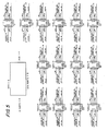
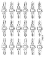
- Figs. 5 and 6 comprise a schematic circuit diagram of an array of 32 switches according to an illustrative embodiment.
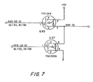
- Figs. 7 and 8 are circuit diagrams of driver circuits for driving switches such as those disclosed in Figs. 5 and 6 .
- Fig. 9 is an enlarged view of one of the switches of the array shown in Figs. 5 and 6 .
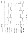
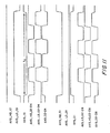
- Figs. 10 and 11 are waveform diagrams useful in illustrating a method for driving switches of the array of Figs. 1 and 2 with a reduced number of drivers.
- Fig. 1 illustrates a switching array network 11 according to an illustrative embodiment.
- the system 11 of Fig. 1 is a relatively large system comprising a plurality of Nodes 1... Q and an Expansion Array 21 also identified as Node 0.
- each of the nodes e.g. Node 1
- Each of the Nodes 1... Q have a common three stage structure formed of A, B, and C switching arrays, interconnected as shown.
- the Expansion Array comprises a column of "D" switching arrays.
- the A, B, C and D arrays are defined as follows: An array of type A has N inputs and K outputs. An array of type B has M+P inputs and M+P outputs. An array of type C has K inputs and N outputs. An array of type D has Q inputs and Q outputs.
- Node 1 through Q has only arrays of type A, B and C, while Node 0 has only arrays of type D.
- the various arrays may be identified as follows:
- a switch is a device that may be activated to connect one input to one output of the same array.
- Each switch is represented by the notation S ( node, array type, array number, input, output).
- S( I , A , 2 , 1,3 ) denotes the switch that connects input 1 to output 3 of type A array 2 in node 1
- S( 0 , D , 3 , 2 , 5 ) denotes the switch that bridges input 2 with output 5 of the type D array 3 in node 0.
- switches of the A, B, C and D arrays are identified as follows:
- more than one possible path exists between any two I/O points in the network.
- the following procedure is used to determine all possible paths (S1, S2, S3, S4, S5) between two I/O points in the network.
- a key task in a system such as that illustrated in Fig. 1 is to select the appropriate switches in the Nodes I... Q and the Expansion Array 21 to complete a desired cross-connect. For example, if it is desired to connect port “1" ("X" Port) of the A array in Node 1 to port “1" ("Y" Port) of the C array in Node 1, appropriate switches in Node 1 (and no switches in Expansion Array 21) must be selected and closed to create the desired signal path.
- a "path” may comprise a group or set of switches which serially interlink a desired pair of ports ("X" and "Y”) through the hardware system.
- switch selection and interconnection task just discussed would be to employ software to determine the appropriate group of switches in real time during operation of the switching array of Fig. 1 .
- This approach creates tremendous software overhead and complexity.
- this approach is avoided by employing software to first create an array of switch identifiers based on the specific, known switching system architecture, which greatly simplifies selection of appropriate switches to create a desired path during real time operation of a deployed system.
- a switch identifier array is preferably determined and stored in the system as part of the system manufacturing process prior to deployment of the system at an end user site. A relatively straight forward indexing operation may then be used to determine those switches which may be closed to achieve a desired interconnection.
- Figs. 2 and 3 after the switching system architecture is established (step 101), software 61 running on a computer processor 57 generates an array 55 of switch identifiers (step 103), and stores the array 55 in memory 59.
- the array 55 is divided into subarrays, e.g. 71, 73.
- Each sub-array contains all sets of switches S1, S2, S3, S4, S5 which are capable of connecting a selected "X" Port to a selected "Y” Port. For example, all switch sets S A ( 1,1 )...
- Each sub-array is determined by software program steps of software 61, which may, for example, compute either equations 1-5 or equations 6-10 above for the particular port pair (X,Y,) in question.
- software may be written, for example, in C++, or any other suitable language.
- the switch selection software 63 which actually selects a particular switch set (such as switch set S A1 , 1 ) to establish connection between a pair of ports (such as ports 1,1), need only employ an index (e.g. "1,1") during real time operation to access the set 71 of all possible switches for establishing a particular port-to-port connection (step 105, Fig. 4 ). Thereafter, in step 107 of Fig. 4 , for example, the switch selection software may perform a particular switch selection procedure employing various criteria, such as those known to those skilled in the art, for selecting a particular pair of switches from those which are available.
- an index e.g. "1,1”
- Implementation of a cross-connect switching architecture such as that shown in Fig. 1 may be enhanced in certain embodiments by implementing a switching device activation approach which allows the elimination of a number of discrete drivers by counter driving the coils of parasitic EM devices with pulse modulated electromotive force (EMF) to counteract the sympathetic switching of nearby devices.
- EMF pulse modulated electromotive force
- the EMF duty cycle and polarity applied to the parasitic paths is determined by the tolerance of switching EMF and the proximity of the sympathetic EM device to the targeted device within a matrix array. The result is that the EM devices in the parasitic paths are not switched for either possible initial state and the total number of drivers required for large arrays of EM devices such as, for example, relays and solenoids, is greatly reduced. Implementation of the foregoing approach is illustrated in connection with Figs. 5-11 .
- Figs. 5 and 6 depict an array of 32 switching devices S 1 , S 2 , S 3 ... S 32 .
- the particular switching devices depicted are cantilever MEMS switches, but could be other types of switches or relays in other embodiments.
- Each of the switches S 1 ... S 32 includes an activation coil (e.g. 21 in Fig. 9 ), having positive ("Y") and negative ("X") terminals.
- eight positive terminal drivers and four negative terminal drivers suffice to switch ("close") any selected one of the 32 switching devices S 1 ... S 32 .
- the eight positive drivers produce respective drive signals, AYS_01, AYS_02, AYS_03 ... AYS_08; while the four negative drivers produce four respective drive signals AXS_01, AXS_02, AXS_03 and AXS_04.
- Fig. 7 and 8 depict a driver circuit for generating drive signals AXS_01 and AYS_01, respectively. These driver circuits may be conventional MOSFET drivers.
- the driver of Fig. 3 is triggered by gate signals AXS_HD_01 and AXS_LD_01, while that of Fig. 4 is triggered by gates signals AYS_HD_01 and AYS_LD_01.
- a specific MEMS switching device S 27 is shown enlarged in Fig. 9 . It may be seen that the coil 21 of this device S 27 is driven by drive signals AYS_01 and AXS_01. Pins 7 and 4 are "signal-in” pins and pins 8 and 3 are “signal returns,” respectively.
- the temporary magnetic field created by an energy pulse to the coil 21 starts the respective cantilever S 23 , S 24 to pull and close the respective signal paths.
- the cantilevers 23, 24 are held in place by a fixed magnet after the activation pulse to the coil 21 terminates.
- Fig. 10 illustrates the pulse waveforms utilized when it is desired to set switch S 27 , i.e. close cantilevers 23, 24.
- AXS_01 rises to a constant positive voltage level for a time interval t 1 , which may be for example, 200 microseconds.
- AYS_01 drops to a constant negative voltage level over the same interval t 1 .
- the other "X" drive signals AXS_02, AXS_03 and AXS_04 are pulsed with a periodic pulse train which alternates between a positive and a negative voltage level.
- the other "Y" drive signals AYS_02... AYS-08 are driven with a pulse train which may be the same as, but opposite in polarity, to that driving AXS_02 - 04.
- switch S 27 is provided with the energy necessary to activate or "close” it, while the pulse modulated energy prevents false triggering of other switching devices in the array.
- three other switches in S 25 , S 29 , S 31 in the 32 switch array of Figs. 5 and 6 are driven by the output AYS_01 of the driver circuit shown in Fig. 8 .
- each of these other switches receives a respective one of the modulated "X" drive signals AXS_02, AXS_03 and AXS_04, which prevents triggering of these three switches S 25 , S 29 , S 31 .
- AXS_01 comprises a negative pulse of duration t 2
- AYS_01 comprises a positive pulse of duration t 2
- the waveforms for AXS_02 - 04 and AYS_02 -08 are the same as those of Fig. 10 ; thus achieving the resetting of switch S 27 without false triggering of other switches in the array.
Landscapes
- Engineering & Computer Science (AREA)
- Computer Networks & Wireless Communication (AREA)
- Signal Processing (AREA)
- Use Of Switch Circuits For Exchanges And Methods Of Control Of Multiplex Exchanges (AREA)
Description
- The present invention relates in general to telecommunications switching systems and more particularly to a large, efficient and cost effective cross-connect switching architecture.
- Digital cross-connect systems are an integral part of today's modem telecommunications transport network. They are increasingly used by all service providers including exchange carriers, long distance carriers, and competitive by-pass carriers. Significant technology advancements have allowed digital cross-connect systems to evolve from narrowband grooming and test applications to cross-connect of larger network signals in wideband and broadband frequency domains.
- A broadband system is typically used to terminate high speed SONET optical and electrical signals in order to path terminate and groom lower speed broadband signals. The broadband system also supports performance monitoring and test access functions. Typical broadband cross-connect systems use either single stage or three stage Clos matrix architecture. In the three stage matrix architecture, the cross-connect includes switches grouped into an originating stage, a center stage, and a terminating stage. The three stage matrix architecture is best suited for maximum capacity applications for cross-connecting a large volume of signals. The single stage matrix architecture organizes the single stage matrices in rows and columns, which results in a higher number of switches than the three stage architecture.
The paper "Adaptive Routing in High-Radix Clos Network", John Kim et al, November 2006, XP031044199 dislcoses a adaptive routing techniques in Clos networks to reduce latency and reduce variance in packet latency, - While the Clos three stage architecture has been a staple of high capacity cross-connect arrays, the inventors have recognized a need for even higher capacity arrays. Embodiments configured according to invention facilitate providing such capacity.
There is provided a switching array comprising: (a) a plurality of three stage switching arrays; and (b) an expansion switching array, wherein a second stage of each of the three stage switching arrays includes an expansion section comprising switches which facilitate interconnection of each three stage array to the expansion switching array; (c) wherein each of the plurality of three stage switching arrays comprises a first stage array having N inputs and K outputs and a third stage array having K inputs and N outputs, each second stage array of each three stage switching array receiving M local inputs from the first stage array and providing M local outputs to the third stage switching array, each second stage switching array further providing P outputs to the expansion array and receiving P inputs from the expansion array, where K, N, M and P are integers; and (d) wherein the switching array comprises a plurality of nodes and wherein, in each node, there are K second stage arrays, M first stage arrays, and M third stage arrays, and wherein the number of expansion switching arrays in the expansion array is equal to K × P.
A selection of optional features of the claims are set out in the dependent claims. -
Fig. 1 is a schematic diagram of a switching array according to an illustrative embodiment. -
Fig. 2 is a schematic diagram of an array of switch identifiers according to an illustrative embodiment. -
Fig. 3 is a block diagram of a computer processor and associated memory according to an illustrative embodiment. -
Fig. 4 is a flow diagram of a switch selection process employing the illustrative embodiment. -
Figs. 5 and6 comprise a schematic circuit diagram of an array of 32 switches according to an illustrative embodiment. -
Figs. 7 and8 are circuit diagrams of driver circuits for driving switches such as those disclosed inFigs. 5 and6 . -
Fig. 9 is an enlarged view of one of the switches of the array shown inFigs. 5 and6 . -
Figs. 10 and11 are waveform diagrams useful in illustrating a method for driving switches of the array ofFigs. 1 and2 with a reduced number of drivers. -
Fig. 1 illustrates a switching array network 11 according to an illustrative embodiment. The system 11 ofFig. 1 is a relatively large system comprising a plurality ofNodes 1... Q and anExpansion Array 21 also identified as Node 0. InFig. 1 , each of the nodes e.g.Node 1, is drawn twice, once at the left ofExpansion Array 21 and once to the right of theArray 21. This depiction is employed so that the interconnections, e.g. 15, 17, to the Expansion Array from the left and right side of the "B" arrays in each of the nodes do not overlap other portions of the drawing and are therefore more clearly shown. - Each of the
Nodes 1... Q have a common three stage structure formed of A, B, and C switching arrays, interconnected as shown. The Expansion Array comprises a column of "D" switching arrays. The A, B, C and D arrays are defined as follows:
An array of type A has N inputs and K outputs.
An array of type B has M+P inputs and M+P outputs.
An array of type C has K inputs and N outputs.
An array of type D has Q inputs and Q outputs. - Further with respect to the topology of
Fig. 1 , it may be observed thatNode 1 through Q has only arrays of type A, B and C, while Node 0 has only arrays of type D. As to the number of arrays, there are M arrays of type A in each ofnode 1 thru node Q, there are K arrays of type B in each ofNode 1 thru Node Q, there are M arrays of type C in each ofnode 1 thru node Q, and there are R arrays of type D in Node 0 where R = KXP. The various arrays may be identified as follows: - A( m ) denotes a type A array m in node q where m = 1 .. M; and q = 1 .. Q.
- B( k ) denotes a type B array k in node q where k = 1.. K; and q = 1.. Q.
- C( m ) denotes a type C array m in node q where m = I .. M; and q = 1 Q.
- D(r) denotes a type D array r in node 0 where r = P(k-1)+p;k = 1.. K; p = 1 .. P.
- The interconnection of the respective A, B, C and D arrays are defined as follows:
- 1. Output k of array A(m) in node q connects to input m of array B( k ) in the same node q, where m = 1 M and k = 1 .. K.
- 2. Output m of array B( k ) in node q connects to input k of array C(m) in the same node q, where m =1.. M and k = 1.. K.
- 3. Output M+p of array B( k ) in Node q connects to input q of array D(r=P(k-1)+p) in Node 0, where p = 1.. P; k = 1.. K; and q = 1 .. Q.
- 4. Output q of array D(r=P(k-l)+p) in Node 0 connects to input M+p of array B( k ) in Node q, where q = 1.. Q; k = 1.. K; and p = 1 .. P.
- In the switching array of
Fig. 1 , a switch is a device that may be activated to connect one input to one output of the same array. Each switch is represented by the notation S (node, array type, array number, input, output). For example, S( I,A,2,1,3 ) denotes the switch that connectsinput 1 tooutput 3 oftype A array 2 innode 1; S( 0 , D,3,2,5 ) denotes the switch that bridgesinput 2 withoutput 5 of thetype D array 3 in node 0. - Employing the switch notation convention just discussed, the switches of the A, B, C and D arrays are identified as follows:
- 1. The switch that connects input x to output k of the type A array m in node q is identified by S(q,A,m,x;k), where q = 1 .. Q; m = 1.. M; x = 1.. N; k = I .. K.
- 2. The switch that connects input m to output n of the type B array k in node q is identified by S(q,B,k,m,n), where q = 1.. Q; k = 1.. K; m = 1 .. M; n = 1 .. M.
- 3. The switch that connects input k to output y of the type C array m in node q is identified by S (q,C,m,k,y), where q = 1.. Q; m = 1 .. M; k = 1.. K; y = 1 .. N.
- 4. The switch that connects input p to output t of the type D array r in node 0 is identified by S(0, D,r,p,t), where r = 1.. P(k-1)+p; p = 1 P; t = 1 .. P.
- As may be appreciated, more than one possible path (more than one set of switches (S1, S2, S3, S4, S5)) exists between any two I/O points in the network. In the illustrative embodiment, the following procedure is used to determine all possible paths (S1, S2, S3, S4, S5) between two I/O points in the network.
- First, the following constants are defined:
- Q = number of I/O nodes in the network
- N = number of inputs on each type A array
- N = also number of outputs on each type C array
- K = number of outputs on each type A array
- K = also number of inputs on each type C array
- M = number of local inputs (from type A array) on each type B array
- M = also number of local outputs (to type C array) on each type B array
- P = number of foreign inputs (from type D array) on each type B array
- P = number of foreign outputs (to type D array) on each type B array
- q = int(X/(N x M x Q)) + 1
- m = int(Xl(N x Mx q)) + 1
- n =X- int(X/(q x m x M) x N
- As those skilled in the art will appreciate, a key task in a system such as that illustrated in
Fig. 1 is to select the appropriate switches in the Nodes I... Q and theExpansion Array 21 to complete a desired cross-connect. For example, if it is desired to connect port "1" ("X" Port) of the A array inNode 1 to port "1" ("Y" Port) of the C array inNode 1, appropriate switches in Node 1 (and no switches in Expansion Array 21) must be selected and closed to create the desired signal path. Thus, as noted above, a "path" may comprise a group or set of switches which serially interlink a desired pair of ports ("X" and "Y") through the hardware system. - One approach to accomplishing the switch selection and interconnection task just discussed would be to employ software to determine the appropriate group of switches in real time during operation of the switching array of
Fig. 1 . This approach creates tremendous software overhead and complexity. According to the preferred embodiment, this approach is avoided by employing software to first create an array of switch identifiers based on the specific, known switching system architecture, which greatly simplifies selection of appropriate switches to create a desired path during real time operation of a deployed system. Thus, such a switch identifier array is preferably determined and stored in the system as part of the system manufacturing process prior to deployment of the system at an end user site. A relatively straight forward indexing operation may then be used to determine those switches which may be closed to achieve a desired interconnection. - More particularly, in the illustrative embodiment depicted in
Figs. 2 and 3 , and as shown inFig. 4 , after the switching system architecture is established (step 101),software 61 running on acomputer processor 57 generates anarray 55 of switch identifiers (step 103), and stores thearray 55 inmemory 59. As shown inFig. 2 , thearray 55 is divided into subarrays, e.g. 71, 73. Each sub-array contains all sets of switches S1, S2, S3, S4, S5 which are capable of connecting a selected "X" Port to a selected "Y" Port. For example, all switch sets SA(1,1)... SN(1,1) for connecting "X"Port 1 to "Y"Port 1 are stored insub-array 71, while all switch sets SA(1,2)... SN(1,2) for connecting "X"Port 1 with "Y"Port 2 are stored insub-array 73, and so forth. Each sub-array is determined by software program steps ofsoftware 61, which may, for example, compute either equations 1-5 or equations 6-10 above for the particular port pair (X,Y,) in question. Such software may be written, for example, in C++, or any other suitable language. - Once the array of
Fig. 2 has been generated, for example, prior to shipping and deployment of a switching array such as that shown inFig. 1 , theswitch selection software 63, which actually selects a particular switch set (such as switch set SA1,1) to establish connection between a pair of ports (such asports 1,1), need only employ an index (e.g. "1,1") during real time operation to access theset 71 of all possible switches for establishing a particular port-to-port connection (step 105,Fig. 4 ). Thereafter, instep 107 ofFig. 4 , for example, the switch selection software may perform a particular switch selection procedure employing various criteria, such as those known to those skilled in the art, for selecting a particular pair of switches from those which are available. - Implementation of a cross-connect switching architecture such as that shown in
Fig. 1 may be enhanced in certain embodiments by implementing a switching device activation approach which allows the elimination of a number of discrete drivers by counter driving the coils of parasitic EM devices with pulse modulated electromotive force (EMF) to counteract the sympathetic switching of nearby devices. According to an illustrative embodiment, the EMF duty cycle and polarity applied to the parasitic paths is determined by the tolerance of switching EMF and the proximity of the sympathetic EM device to the targeted device within a matrix array. The result is that the EM devices in the parasitic paths are not switched for either possible initial state and the total number of drivers required for large arrays of EM devices such as, for example, relays and solenoids, is greatly reduced. Implementation of the foregoing approach is illustrated in connection withFigs. 5-11 . -
Figs. 5 and6 depict an array of 32 switching devices S1, S2, S3... S32. The particular switching devices depicted are cantilever MEMS switches, but could be other types of switches or relays in other embodiments. - Each of the switches S1... S32 includes an activation coil (e.g. 21 in
Fig. 9 ), having positive ("Y") and negative ("X") terminals. According to the illustrative embodiment, eight positive terminal drivers and four negative terminal drivers suffice to switch ("close") any selected one of the 32 switching devices S1... S32. The eight positive drivers produce respective drive signals, AYS_01, AYS_02, AYS_03 ... AYS_08; while the four negative drivers produce four respective drive signals AXS_01, AXS_02, AXS_03 and AXS_04. -
Fig. 7 and8 depict a driver circuit for generating drive signals AXS_01 and AYS_01, respectively. These driver circuits may be conventional MOSFET drivers. The driver ofFig. 3 is triggered by gate signals AXS_HD_01 and AXS_LD_01, while that ofFig. 4 is triggered by gates signals AYS_HD_01 and AYS_LD_01. - A specific MEMS switching device S27 is shown enlarged in
Fig. 9 . It may be seen that thecoil 21 of this device S27 is driven by drive signals AYS_01 and AXS_01.Pins coil 21 starts the respective cantilever S23, S24 to pull and close the respective signal paths. Thecantilevers coil 21 terminates. -
Fig. 10 illustrates the pulse waveforms utilized when it is desired to set switch S27, i.e.close cantilevers - In this manner, only switch S27 is provided with the energy necessary to activate or "close" it, while the pulse modulated energy prevents false triggering of other switching devices in the array. As may be appreciated, three other switches in S25, S29, S31 in the 32 switch array of
Figs. 5 and6 are driven by the output AYS_01 of the driver circuit shown inFig. 8 . However, each of these other switches receives a respective one of the modulated "X" drive signals AXS_02, AXS_03 and AXS_04, which prevents triggering of these three switches S25, S29, S31. - To clear or reset switch S27, the energy waveforms depicted in
Fig. 11 are used. In this case, AXS_01 comprises a negative pulse of duration t2, while AYS_01 comprises a positive pulse of duration t2. The waveforms for AXS_02 - 04 and AYS_02 -08 are the same as those ofFig. 10 ; thus achieving the resetting of switch S27 without false triggering of other switches in the array. - With respect to switch S27, the pulse interval and voltage level supplied by AXS_01 and AYS_01 may be those typically necessary to close the switch. Such levels and durations will typically vary depending on the type of switch used, e.g. MEMS switches or electromechanical relays or solenoids. Additionally, the voltage levels and duty cycle of the pulse modulated waveforms, e.g. AXS_02, AXS_03, AXS_04 in
Fig. 10 , will vary with the application, but are selected in each application to be sufficient to prevent false triggering of other devices in the array. Waveforms analogous to those shown inFigs. 10 and11 are used to set and reset any specific one of the other switches in the 32 switch array. With respect to the array ofFigs. 5 and6 , it may be observed that such an array would conventionally require 4x8+4 (N●M+N) = 36 drivers, whereas the illustrative embodiment employs 12 drivers. - Methods according to the illustrative embodiments are effective in addressing EM device arrays that are symmetric (N=M), asymmetric (N>M or N<M), or asymmetric plus non orthogonal (an array composed of multi asymmetric sub arrays with various N or M segments).
- Those skilled in the art will appreciate that various adaptations and modifications of the just described preferred embodiment can be configured. Therefore, it is to be understood that, within the scope of the appended claims, the invention may be practiced other than as specifically described herein.


and the set of switches S1, S2, S3, S4, S5 for connecting a port "X" in one Node with a port "Y" in a different Node is determined as follows for (t = 1.. .. P), for (h = 1 .. K) and for a port (y=1..N):





Claims (6)
- A switching array comprising:(a) a plurality of three stage switching arrays (Node I ... Node Q); and(b) an expansion switching array (21), wherein a second stage (B) of each of the three stage switching arrays (Node 1 ... Node Q) includes an expansion section comprising switches which facilitate interconnection of each three stage array (Node I ... Node Q) to the expansion switching array (21);(c) wherein each of the plurality of three stage switching arrays (Node 1 ...
Node Q) comprises a first stage array (A) having N inputs and K outputs and a third stage array (C) having K inputs and N outputs, each second stage array (B) of each three stage switching array (Node I ... Node Q) receiving M local inputs from the first stage array (A) and providing M local outputs to the third stage switching array (C), each second stage switching array (B) further providing P outputs to the expansion array (21) and receiving P inputs from the expansion array (21), where K, N, M and P are integers; and(d) wherein the switching array comprises a plurality of nodes and wherein, in each node, there are K second stage arrays (B), M first stage arrays (A), and M third stage arrays (C), and wherein the number of expansion switching arrays in the expansion array (21) is equal to K × P. - The switching array of claim 1:wherein the expansion section of each second stage array (B) of each three stage switching array (Node 1 ... Node Q) includes a plurality of expansion outputs, each connected as an input to a respective expansion switching array (21) and wherein each respective expansion switching array (21) provides a plurality of expansion outputs, each connected as an input back to a respective second stage switching array (B).
- The switching array of claim 1 or 2 wherein each expansion switching array (21) is a square array (D) having Q inputs and Q outputs, where Q is an integer.
- The switching array of claim 1 or 2 wherein the expansion array (21) comprises a single column of square switching arrays (D).
- The switching array of claim 1 or 2 wherein the expansion array (21) includes a plurality of square arrays (D), each having Q inputs and Q outputs and wherein the second stages (B) of the three stage arrays (Node I ... Node Q) each include 1... M+1 ... M+P vertical stages which connect to the square arrays of the expansion array (21).
- The switching array of claim 4 wherein each square array has Q inputs and Q outputs and wherein the second stages of the three stage arrays each include 1 ... M+1... M+P vertical stages which connect to the square arrays of the expansion array.
Priority Applications (2)
| Application Number | Priority Date | Filing Date | Title |
|---|---|---|---|
| PL07869286T PL2095583T3 (en) | 2006-12-19 | 2007-12-14 | Matrix expansion lattice |
| EP13179776.3A EP2680516A1 (en) | 2006-12-19 | 2007-12-14 | Matrix expansion lattice |
Applications Claiming Priority (7)
| Application Number | Priority Date | Filing Date | Title |
|---|---|---|---|
| US87072106P | 2006-12-19 | 2006-12-19 | |
| US87110306P | 2006-12-20 | 2006-12-20 | |
| US87110006P | 2006-12-20 | 2006-12-20 | |
| US11/950,272 US7804825B2 (en) | 2006-12-20 | 2007-12-04 | Matrix expansion lattice |
| US11/950,253 US7956668B2 (en) | 2006-12-20 | 2007-12-04 | Spectral predictive switching device activation |
| US11/950,230 US20080143473A1 (en) | 2006-12-19 | 2007-12-04 | Digital Cross-Connect Path Selection Method |
| PCT/US2007/087604 WO2008079744A2 (en) | 2006-12-19 | 2007-12-14 | Switch matrix expansion lattice |
Publications (3)
| Publication Number | Publication Date |
|---|---|
| EP2095583A2 EP2095583A2 (en) | 2009-09-02 |
| EP2095583A4 EP2095583A4 (en) | 2011-02-16 |
| EP2095583B1 true EP2095583B1 (en) | 2013-08-14 |
Family
ID=39563169
Family Applications (2)
| Application Number | Title | Priority Date | Filing Date |
|---|---|---|---|
| EP07869286.0A Not-in-force EP2095583B1 (en) | 2006-12-19 | 2007-12-14 | Matrix expansion lattice |
| EP13179776.3A Withdrawn EP2680516A1 (en) | 2006-12-19 | 2007-12-14 | Matrix expansion lattice |
Family Applications After (1)
| Application Number | Title | Priority Date | Filing Date |
|---|---|---|---|
| EP13179776.3A Withdrawn EP2680516A1 (en) | 2006-12-19 | 2007-12-14 | Matrix expansion lattice |
Country Status (6)
| Country | Link |
|---|---|
| EP (2) | EP2095583B1 (en) |
| DK (1) | DK2095583T3 (en) |
| ES (1) | ES2434765T3 (en) |
| PL (1) | PL2095583T3 (en) |
| PT (1) | PT2095583E (en) |
| WO (1) | WO2008079744A2 (en) |
Family Cites Families (5)
| Publication number | Priority date | Publication date | Assignee | Title |
|---|---|---|---|---|
| US3582560A (en) * | 1968-08-02 | 1971-06-01 | Communications & Systems Inc | Multistage telephone switching system for different priority users |
| DE3802579A1 (en) * | 1988-01-29 | 1989-08-10 | Ant Nachrichtentech | THREE-STAGE NON-BLOCKING DOMESTIC |
| US6696917B1 (en) * | 2000-09-21 | 2004-02-24 | Nortel Networks Limited | Folded Clos architecture switching |
| AU2003225284A1 (en) * | 2002-05-02 | 2003-11-17 | Ciena Corporation | Distribution stage for enabling efficient expansion of a switching network |
| US7675909B2 (en) * | 2004-12-15 | 2010-03-09 | Tellabs Operations, Inc. | Method and apparatus for horizontally slicing a multi-stage switch fabric |
-
2007
- 2007-12-14 EP EP07869286.0A patent/EP2095583B1/en not_active Not-in-force
- 2007-12-14 ES ES07869286T patent/ES2434765T3/en active Active
- 2007-12-14 DK DK07869286.0T patent/DK2095583T3/en active
- 2007-12-14 EP EP13179776.3A patent/EP2680516A1/en not_active Withdrawn
- 2007-12-14 WO PCT/US2007/087604 patent/WO2008079744A2/en not_active Ceased
- 2007-12-14 PT PT78692860T patent/PT2095583E/en unknown
- 2007-12-14 PL PL07869286T patent/PL2095583T3/en unknown
Also Published As
| Publication number | Publication date |
|---|---|
| WO2008079744A3 (en) | 2008-08-21 |
| PL2095583T3 (en) | 2014-03-31 |
| PT2095583E (en) | 2013-11-13 |
| EP2095583A4 (en) | 2011-02-16 |
| ES2434765T3 (en) | 2013-12-17 |
| EP2680516A1 (en) | 2014-01-01 |
| DK2095583T3 (en) | 2013-11-18 |
| WO2008079744A2 (en) | 2008-07-03 |
| EP2095583A2 (en) | 2009-09-02 |
Similar Documents
| Publication | Publication Date | Title |
|---|---|---|
| EP0761071B1 (en) | Optical telecommunications network | |
| EP0872087B1 (en) | Packet routing | |
| US6696917B1 (en) | Folded Clos architecture switching | |
| CN102740177B (en) | Non-blocking expandable multistage photoswitch array and working method thereof | |
| JP3475900B2 (en) | Arbitration method and arbiter circuit using the same | |
| CA1295040C (en) | Optical switching system | |
| US7804825B2 (en) | Matrix expansion lattice | |
| CN100587509C (en) | Efficient switch structure with reduced wire tip length | |
| DE69837609T2 (en) | COMMUNICATION NETWORK | |
| EP0574484A1 (en) | Communications switching network | |
| GB2281472A (en) | Telecommunications switching element | |
| EP2680516A1 (en) | Matrix expansion lattice | |
| RU2121230C1 (en) | Optical switching device for connecting optical data locations | |
| US20110103798A1 (en) | Add-drop benes networks | |
| US6430179B1 (en) | Three stage router for broadcast application | |
| KR100262474B1 (en) | Methods and systems for directly connecting and reswitching digital cross-connect networks | |
| US20080143473A1 (en) | Digital Cross-Connect Path Selection Method | |
| US7956668B2 (en) | Spectral predictive switching device activation | |
| EP0534232A1 (en) | An apparatus and method for connecting inter-SRM highways | |
| Pan et al. | Recent developments in optical multistage networks | |
| Vaez et al. | Blocking performance with crosstalk consideration of the photonic switching networks based on electrooptical directional couplers | |
| Geldenhuys et al. | Selecting fibre delay line distributions for travelling buffers in an all-optical packet switched cross-connect | |
| Suliman et al. | Design of a Control Algorithm for a 2× 3 Optical Switch | |
| US3515811A (en) | Marking circuit for a relay crosspoint network | |
| Kleban et al. | SMM Clos-Network Switches under SD Algorithm |
Legal Events
| Date | Code | Title | Description |
|---|---|---|---|
| PUAI | Public reference made under article 153(3) epc to a published international application that has entered the european phase |
Free format text: ORIGINAL CODE: 0009012 |
|
| 17P | Request for examination filed |
Effective date: 20090612 |
|
| AK | Designated contracting states |
Kind code of ref document: A2 Designated state(s): AT BE BG CH CY CZ DE DK EE ES FI FR GB GR HU IE IS IT LI LT LU LV MC MT NL PL PT RO SE SI SK TR |
|
| DAX | Request for extension of the european patent (deleted) | ||
| A4 | Supplementary search report drawn up and despatched |
Effective date: 20110119 |
|
| RIC1 | Information provided on ipc code assigned before grant |
Ipc: H04L 12/56 20060101AFI20110706BHEP |
|
| REG | Reference to a national code |
Ref country code: DE Ref legal event code: R079 Ref document number: 602007032315 Country of ref document: DE Free format text: PREVIOUS MAIN CLASS: H04L0012560000 Ipc: H04L0012933000 |
|
| GRAP | Despatch of communication of intention to grant a patent |
Free format text: ORIGINAL CODE: EPIDOSNIGR1 |
|
| RIC1 | Information provided on ipc code assigned before grant |
Ipc: H04L 12/933 20130101AFI20130204BHEP Ipc: H04L 12/931 20130101ALI20130204BHEP |
|
| GRAS | Grant fee paid |
Free format text: ORIGINAL CODE: EPIDOSNIGR3 |
|
| GRAA | (expected) grant |
Free format text: ORIGINAL CODE: 0009210 |
|
| AK | Designated contracting states |
Kind code of ref document: B1 Designated state(s): AT BE BG CH CY CZ DE DK EE ES FI FR GB GR HU IE IS IT LI LT LU LV MC MT NL PL PT RO SE SI SK TR |
|
| REG | Reference to a national code |
Ref country code: GB Ref legal event code: FG4D |
|
| REG | Reference to a national code |
Ref country code: AT Ref legal event code: REF Ref document number: 627386 Country of ref document: AT Kind code of ref document: T Effective date: 20130815 Ref country code: CH Ref legal event code: EP |
|
| REG | Reference to a national code |
Ref country code: IE Ref legal event code: FG4D |
|
| REG | Reference to a national code |
Ref country code: DE Ref legal event code: R096 Ref document number: 602007032315 Country of ref document: DE Effective date: 20131010 |
|
| REG | Reference to a national code |
Ref country code: PT Ref legal event code: SC4A Free format text: AVAILABILITY OF NATIONAL TRANSLATION Effective date: 20131106 |
|
| REG | Reference to a national code |
Ref country code: DK Ref legal event code: T3 Effective date: 20131112 |
|
| REG | Reference to a national code |
Ref country code: SE Ref legal event code: TRGR |
|
| REG | Reference to a national code |
Ref country code: NL Ref legal event code: T3 |
|
| REG | Reference to a national code |
Ref country code: ES Ref legal event code: FG2A Ref document number: 2434765 Country of ref document: ES Kind code of ref document: T3 Effective date: 20131217 |
|
| REG | Reference to a national code |
Ref country code: LT Ref legal event code: MG4D |
|
| PG25 | Lapsed in a contracting state [announced via postgrant information from national office to epo] |
Ref country code: LT Free format text: LAPSE BECAUSE OF FAILURE TO SUBMIT A TRANSLATION OF THE DESCRIPTION OR TO PAY THE FEE WITHIN THE PRESCRIBED TIME-LIMIT Effective date: 20130814 Ref country code: CY Free format text: LAPSE BECAUSE OF FAILURE TO SUBMIT A TRANSLATION OF THE DESCRIPTION OR TO PAY THE FEE WITHIN THE PRESCRIBED TIME-LIMIT Effective date: 20130807 Ref country code: IS Free format text: LAPSE BECAUSE OF FAILURE TO SUBMIT A TRANSLATION OF THE DESCRIPTION OR TO PAY THE FEE WITHIN THE PRESCRIBED TIME-LIMIT Effective date: 20131214 |
|
| REG | Reference to a national code |
Ref country code: GR Ref legal event code: EP Ref document number: 20130402380 Country of ref document: GR Effective date: 20140102 |
|
| PG25 | Lapsed in a contracting state [announced via postgrant information from national office to epo] |
Ref country code: SI Free format text: LAPSE BECAUSE OF FAILURE TO SUBMIT A TRANSLATION OF THE DESCRIPTION OR TO PAY THE FEE WITHIN THE PRESCRIBED TIME-LIMIT Effective date: 20130814 Ref country code: LV Free format text: LAPSE BECAUSE OF FAILURE TO SUBMIT A TRANSLATION OF THE DESCRIPTION OR TO PAY THE FEE WITHIN THE PRESCRIBED TIME-LIMIT Effective date: 20130814 |
|
| PG25 | Lapsed in a contracting state [announced via postgrant information from national office to epo] |
Ref country code: CY Free format text: LAPSE BECAUSE OF FAILURE TO SUBMIT A TRANSLATION OF THE DESCRIPTION OR TO PAY THE FEE WITHIN THE PRESCRIBED TIME-LIMIT Effective date: 20130814 |
|
| PG25 | Lapsed in a contracting state [announced via postgrant information from national office to epo] |
Ref country code: CZ Free format text: LAPSE BECAUSE OF FAILURE TO SUBMIT A TRANSLATION OF THE DESCRIPTION OR TO PAY THE FEE WITHIN THE PRESCRIBED TIME-LIMIT Effective date: 20130814 Ref country code: RO Free format text: LAPSE BECAUSE OF FAILURE TO SUBMIT A TRANSLATION OF THE DESCRIPTION OR TO PAY THE FEE WITHIN THE PRESCRIBED TIME-LIMIT Effective date: 20130814 Ref country code: EE Free format text: LAPSE BECAUSE OF FAILURE TO SUBMIT A TRANSLATION OF THE DESCRIPTION OR TO PAY THE FEE WITHIN THE PRESCRIBED TIME-LIMIT Effective date: 20130814 Ref country code: SK Free format text: LAPSE BECAUSE OF FAILURE TO SUBMIT A TRANSLATION OF THE DESCRIPTION OR TO PAY THE FEE WITHIN THE PRESCRIBED TIME-LIMIT Effective date: 20130814 |
|
| PLBE | No opposition filed within time limit |
Free format text: ORIGINAL CODE: 0009261 |
|
| STAA | Information on the status of an ep patent application or granted ep patent |
Free format text: STATUS: NO OPPOSITION FILED WITHIN TIME LIMIT |
|
| 26N | No opposition filed |
Effective date: 20140515 |
|
| REG | Reference to a national code |
Ref country code: DE Ref legal event code: R097 Ref document number: 602007032315 Country of ref document: DE Effective date: 20140515 |
|
| REG | Reference to a national code |
Ref country code: HU Ref legal event code: AG4A Ref document number: E020235 Country of ref document: HU |
|
| PG25 | Lapsed in a contracting state [announced via postgrant information from national office to epo] |
Ref country code: BG Free format text: LAPSE BECAUSE OF FAILURE TO SUBMIT A TRANSLATION OF THE DESCRIPTION OR TO PAY THE FEE WITHIN THE PRESCRIBED TIME-LIMIT Effective date: 20130814 |
|
| PG25 | Lapsed in a contracting state [announced via postgrant information from national office to epo] |
Ref country code: MT Free format text: LAPSE BECAUSE OF FAILURE TO SUBMIT A TRANSLATION OF THE DESCRIPTION OR TO PAY THE FEE WITHIN THE PRESCRIBED TIME-LIMIT Effective date: 20130814 |
|
| REG | Reference to a national code |
Ref country code: FR Ref legal event code: PLFP Year of fee payment: 9 |
|
| PGFP | Annual fee paid to national office [announced via postgrant information from national office to epo] |
Ref country code: GR Payment date: 20151112 Year of fee payment: 9 Ref country code: FI Payment date: 20151209 Year of fee payment: 9 Ref country code: DK Payment date: 20151210 Year of fee payment: 9 Ref country code: DE Payment date: 20151208 Year of fee payment: 9 Ref country code: GB Payment date: 20151209 Year of fee payment: 9 Ref country code: IE Payment date: 20151209 Year of fee payment: 9 Ref country code: CH Payment date: 20151211 Year of fee payment: 9 |
|
| PGFP | Annual fee paid to national office [announced via postgrant information from national office to epo] |
Ref country code: PL Payment date: 20151119 Year of fee payment: 9 Ref country code: MC Payment date: 20151110 Year of fee payment: 9 Ref country code: HU Payment date: 20151112 Year of fee payment: 9 Ref country code: ES Payment date: 20151112 Year of fee payment: 9 Ref country code: NL Payment date: 20151210 Year of fee payment: 9 Ref country code: BE Payment date: 20151207 Year of fee payment: 9 Ref country code: SE Payment date: 20151211 Year of fee payment: 9 Ref country code: AT Payment date: 20151125 Year of fee payment: 9 Ref country code: PT Payment date: 20151214 Year of fee payment: 9 Ref country code: FR Payment date: 20151110 Year of fee payment: 9 |
|
| PGFP | Annual fee paid to national office [announced via postgrant information from national office to epo] |
Ref country code: LU Payment date: 20160106 Year of fee payment: 9 |
|
| PGFP | Annual fee paid to national office [announced via postgrant information from national office to epo] |
Ref country code: IT Payment date: 20151221 Year of fee payment: 9 |
|
| PGFP | Annual fee paid to national office [announced via postgrant information from national office to epo] |
Ref country code: TR Payment date: 20141214 Year of fee payment: 8 |
|
| PG25 | Lapsed in a contracting state [announced via postgrant information from national office to epo] |
Ref country code: BE Free format text: LAPSE BECAUSE OF NON-PAYMENT OF DUE FEES Effective date: 20161231 |
|
| REG | Reference to a national code |
Ref country code: DE Ref legal event code: R119 Ref document number: 602007032315 Country of ref document: DE |
|
| PG25 | Lapsed in a contracting state [announced via postgrant information from national office to epo] |
Ref country code: FI Free format text: LAPSE BECAUSE OF NON-PAYMENT OF DUE FEES Effective date: 20161214 |
|
| REG | Reference to a national code |
Ref country code: DK Ref legal event code: EBP Effective date: 20161231 Ref country code: CH Ref legal event code: PL |
|
| REG | Reference to a national code |
Ref country code: SE Ref legal event code: EUG |
|
| REG | Reference to a national code |
Ref country code: NL Ref legal event code: MM Effective date: 20170101 |
|
| REG | Reference to a national code |
Ref country code: AT Ref legal event code: MM01 Ref document number: 627386 Country of ref document: AT Kind code of ref document: T Effective date: 20161214 |
|
| GBPC | Gb: european patent ceased through non-payment of renewal fee |
Effective date: 20161214 |
|
| PG25 | Lapsed in a contracting state [announced via postgrant information from national office to epo] |
Ref country code: PT Free format text: LAPSE BECAUSE OF NON-PAYMENT OF DUE FEES Effective date: 20170614 Ref country code: SE Free format text: LAPSE BECAUSE OF NON-PAYMENT OF DUE FEES Effective date: 20161215 |
|
| PG25 | Lapsed in a contracting state [announced via postgrant information from national office to epo] |
Ref country code: MC Free format text: LAPSE BECAUSE OF NON-PAYMENT OF DUE FEES Effective date: 20170102 Ref country code: NL Free format text: LAPSE BECAUSE OF NON-PAYMENT OF DUE FEES Effective date: 20170101 |
|
| REG | Reference to a national code |
Ref country code: FR Ref legal event code: ST Effective date: 20170831 |
|
| REG | Reference to a national code |
Ref country code: IE Ref legal event code: MM4A |
|
| PG25 | Lapsed in a contracting state [announced via postgrant information from national office to epo] |
Ref country code: CH Free format text: LAPSE BECAUSE OF NON-PAYMENT OF DUE FEES Effective date: 20161231 Ref country code: FR Free format text: LAPSE BECAUSE OF NON-PAYMENT OF DUE FEES Effective date: 20170102 Ref country code: LU Free format text: LAPSE BECAUSE OF NON-PAYMENT OF DUE FEES Effective date: 20161214 Ref country code: AT Free format text: LAPSE BECAUSE OF NON-PAYMENT OF DUE FEES Effective date: 20161214 Ref country code: IT Free format text: LAPSE BECAUSE OF NON-PAYMENT OF DUE FEES Effective date: 20161214 Ref country code: GR Free format text: LAPSE BECAUSE OF NON-PAYMENT OF DUE FEES Effective date: 20170707 Ref country code: LI Free format text: LAPSE BECAUSE OF NON-PAYMENT OF DUE FEES Effective date: 20161231 |
|
| PG25 | Lapsed in a contracting state [announced via postgrant information from national office to epo] |
Ref country code: GB Free format text: LAPSE BECAUSE OF NON-PAYMENT OF DUE FEES Effective date: 20161214 Ref country code: IE Free format text: LAPSE BECAUSE OF NON-PAYMENT OF DUE FEES Effective date: 20161214 Ref country code: DE Free format text: LAPSE BECAUSE OF NON-PAYMENT OF DUE FEES Effective date: 20170701 Ref country code: HU Free format text: LAPSE BECAUSE OF NON-PAYMENT OF DUE FEES Effective date: 20161215 |
|
| PG25 | Lapsed in a contracting state [announced via postgrant information from national office to epo] |
Ref country code: DK Free format text: LAPSE BECAUSE OF NON-PAYMENT OF DUE FEES Effective date: 20161231 |
|
| REG | Reference to a national code |
Ref country code: BE Ref legal event code: MM Effective date: 20161231 |
|
| PG25 | Lapsed in a contracting state [announced via postgrant information from national office to epo] |
Ref country code: PL Free format text: LAPSE BECAUSE OF NON-PAYMENT OF DUE FEES Effective date: 20161214 |
|
| PG25 | Lapsed in a contracting state [announced via postgrant information from national office to epo] |
Ref country code: ES Free format text: LAPSE BECAUSE OF NON-PAYMENT OF DUE FEES Effective date: 20161215 |
|
| REG | Reference to a national code |
Ref country code: ES Ref legal event code: FD2A Effective date: 20181116 |
|
| PG25 | Lapsed in a contracting state [announced via postgrant information from national office to epo] |
Ref country code: TR Free format text: LAPSE BECAUSE OF NON-PAYMENT OF DUE FEES Effective date: 20161214 |