EP2095462B1 - Antenna - Google Patents
Antenna Download PDFInfo
- Publication number
- EP2095462B1 EP2095462B1 EP07824937A EP07824937A EP2095462B1 EP 2095462 B1 EP2095462 B1 EP 2095462B1 EP 07824937 A EP07824937 A EP 07824937A EP 07824937 A EP07824937 A EP 07824937A EP 2095462 B1 EP2095462 B1 EP 2095462B1
- Authority
- EP
- European Patent Office
- Prior art keywords
- antenna
- switch
- antenna elements
- elements
- switch array
- Prior art date
- Legal status (The legal status is an assumption and is not a legal conclusion. Google has not performed a legal analysis and makes no representation as to the accuracy of the status listed.)
- Not-in-force
Links
- 239000004020 conductor Substances 0.000 claims description 8
- 230000005404 monopole Effects 0.000 claims description 7
- 239000006261 foam material Substances 0.000 claims 1
- 230000005540 biological transmission Effects 0.000 description 7
- 230000008878 coupling Effects 0.000 description 2
- 238000010168 coupling process Methods 0.000 description 2
- 238000005859 coupling reaction Methods 0.000 description 2
- 238000010586 diagram Methods 0.000 description 2
- 239000003989 dielectric material Substances 0.000 description 2
- 238000000034 method Methods 0.000 description 2
- 239000006260 foam Substances 0.000 description 1
- 239000011159 matrix material Substances 0.000 description 1
- 239000002184 metal Substances 0.000 description 1
- 238000000926 separation method Methods 0.000 description 1
Images


Classifications
-
- H—ELECTRICITY
- H01—ELECTRIC ELEMENTS
- H01Q—ANTENNAS, i.e. RADIO AERIALS
- H01Q1/00—Details of, or arrangements associated with, antennas
- H01Q1/27—Adaptation for use in or on movable bodies
- H01Q1/28—Adaptation for use in or on aircraft, missiles, satellites, or balloons
-
- H—ELECTRICITY
- H01—ELECTRIC ELEMENTS
- H01Q—ANTENNAS, i.e. RADIO AERIALS
- H01Q19/00—Combinations of primary active antenna elements and units with secondary devices, e.g. with quasi-optical devices, for giving the antenna a desired directional characteristic
- H01Q19/28—Combinations of primary active antenna elements and units with secondary devices, e.g. with quasi-optical devices, for giving the antenna a desired directional characteristic using a secondary device in the form of two or more substantially straight conductive elements
- H01Q19/32—Combinations of primary active antenna elements and units with secondary devices, e.g. with quasi-optical devices, for giving the antenna a desired directional characteristic using a secondary device in the form of two or more substantially straight conductive elements the primary active element being end-fed and elongated
-
- H—ELECTRICITY
- H01—ELECTRIC ELEMENTS
- H01Q—ANTENNAS, i.e. RADIO AERIALS
- H01Q25/00—Antennas or antenna systems providing at least two radiating patterns
- H01Q25/02—Antennas or antenna systems providing at least two radiating patterns providing sum and difference patterns
-
- H—ELECTRICITY
- H01—ELECTRIC ELEMENTS
- H01Q—ANTENNAS, i.e. RADIO AERIALS
- H01Q3/00—Arrangements for changing or varying the orientation or the shape of the directional pattern of the waves radiated from an antenna or antenna system
- H01Q3/24—Arrangements for changing or varying the orientation or the shape of the directional pattern of the waves radiated from an antenna or antenna system varying the orientation by switching energy from one active radiating element to another, e.g. for beam switching
-
- H—ELECTRICITY
- H01—ELECTRIC ELEMENTS
- H01Q—ANTENNAS, i.e. RADIO AERIALS
- H01Q9/00—Electrically-short antennas having dimensions not more than twice the operating wavelength and consisting of conductive active radiating elements
- H01Q9/04—Resonant antennas
- H01Q9/30—Resonant antennas with feed to end of elongated active element, e.g. unipole
- H01Q9/32—Vertical arrangement of element
- H01Q9/36—Vertical arrangement of element with top loading
Definitions
- This invention relates to a multi-element antenna and in particular, but not exclusively, to a multi-element antenna and associated switching arrangement designed for use in a monopulse radar collision avoidance system.
- TCAS Traffic alert and Collision Avoidance System
- Airborne Collision Avoidance System which is fitted to all aircraft over a certain weight and/or passenger carrying capacity, as mandated by the International Civil Aviation Organisation.
- a recent implementation of TCAS employs an eight element circular antenna array which is fed through a conventional Butler matrix to generate circular phase modes in the array. The circular modes are phase shifted and combined in a sum/difference hybrid to provide a monopulse radar system with claimed resolution of 2° or better.
- TCAS relies upon the relative phase of two circular modes to detect a potential hazard and as such is sensitive, in certain mounting arrangements, to multipath reflections from parts of a host airframe leading to reduced resolution and potential false alarms.
- the present invention resides in an antenna, comprising a plurality of top-loaded monopole antenna elements mounted above a ground plane for providing coverage over a predetermined range of angles in azimuth using a plurality of beams, each antenna element having a base section and a top section, wherein a feed conductor extends from an entry point provided in the base section to connect to a top element positioned at the top section, and the feed conductor is surrounded by and insulated from a hollow cylindrical electrically conducting stem section that extends from the base section, where the stem section connects to the ground plane, to a level proximate to but separated from the top element, in combination with a switch array, wherein at least some of said plurality of antenna elements are connected to switches in said switch array and wherein said switch array is operable to connect selected pairs of said antenna elements to a signal path to thereby generate each of said plurality of beams and to establish a virtual short circuit in respect of unselected antenna elements.
- the antenna and associated switch array according to this first aspect of the present invention offers particularly good directionality in comparison with prior art arrangements.
- top-loaded monopole antenna elements make for a particularly low-profile antenna.
- the design of the antenna feed in which a feed conductor is surrounded by a hollow cylindrical stem section, enables the input impedance of the antenna element to be set (e.g. to 50 Ohms) by appropriate dimensioning of the inner diameter of the stem section relative to the diameter of the feed conductor, thus forming a quarter-wave transformer.
- This has the advantage that an external matching transformer for each antenna element is avoided.
- the inventor in this case has noted that with this antenna element design, in which the top element is effectively fed at the top section of the "stem", there is a slight improvement in the operational bandwidth of the antenna element in comparison with prior art designs.
- the match to 50 ohms input impedence is achieved when the antenna is driven in a "sum" mode, that is, when two adjacent antenna elements are driven in phase with equal amplitude.
- At least one of the plurality of antenna elements is a passive reflector element connected permanently to ground and positioned so as to increase the directionality of the antenna within the predetermined range of angles.
- the top element is in the shape of a substantially flat-topped cone.
- each of the plurality of switches has a first pole connected to a first antenna element and a second pole connected to a second antenna element and the switch is operable to connect alternately the first or second pole to a signal path and the unconnected pole to ground.
- each switch in the switch array is implemented using PIN diodes.
- each switch in the switch array is a band-limited shunt multi-throw switch.
- the antenna comprises a pentagonal array of five antenna elements clustered around a central sixth element and at least the central sixth element is permanently connected to ground.
- a further one of the six antenna elements is permanently connected to ground and the remaining four ungrounded antenna elements are connected to the switch array.
- the antenna comprises a square array of four antenna elements for use with the same switch array.
- the present invention also extends to a collision warning or avoidance system having an antenna, in combination with a switch array, according to preferred embodiments of the present invention outlined above.
- Preferred embodiments of the present invention provide an antenna for use in a monopulse radar collision warning/avoidance system and an associated switching arrangement.
- the antennae and associated switching arrangements are designed for use in a frequency range of interest, preferably 1020-1100MHz (the IFF band).
- the antennae and switching arrangements are designed for use in particular as part of a collision warning/avoidance system for aircraft, although preferred embodiments of the present invention may also be applied to other types of craft with a requirement for collision warning/avoidance, e.g. road vehicles or ships.
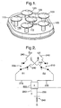
- the antenna comprises a pentagonal array of five antenna elements 100 to 120, surrounding a sixth central antenna element 125.
- the antenna elements 100-125 are mounted on an oval saddle plate 130 which incorporates a ground plane and which enables the antenna to be mounted conveniently on the outer skin of an aircraft fuselage or of another type of vehicle.
- a ridge 135 is provided around the saddle plate 130 for attachment of a radome (not shown in Figure 1 ) to cover and protect the array of antenna elements 100-125.
- the antenna elements 100-125 may be embedded in a dielectric foam or other dielectric material whose dielectric properties may be taken into account in the design of the antenna.
- Each of the antenna elements 100-125 is a top-loaded monopole (TLM) antenna, selected in particular to minimise the overall height of the antenna.
- the antenna elements 100-125 are spaced 72mm apart, which is of the order of one quarter-wavelength in the IFF band. Wider element spacing would be desirable, where mounting constraints permit, to help to avoid problems in a feed network arising from the high inter-element coupling. However, space constraints may impose a closer antenna element spacing, of less than one quarter wavelength.
- the antenna elements 100-120 are located at points on a radius of 55mm from the central element 125. Further preferred and advantageous features of the antenna elements 100-125 will be described below.
- a switching arrangement comprising switches 205 and 210, designated S1 and S2 respectively, each operable to switch between two positions designated 0 and 1 to connect respective pairs of switch outputs, selected from switch outputs designated A, B, C and D in Figure 2 , to one of two signal paths 215, 220, in various combinations.
- the signal paths 215, 220 are linked to a conventional hybrid coupler 225 for coupling sum and difference signal paths 230, 235 respectively to a collision warning/avoidance processor (not shown in Figure 2 ).
- the switch outputs are linked to four of the antenna elements 100-125 of the antenna so that only those four antenna elements are used actively to transmit or receive signals, the remaining two elements being short-circuited permanently to the ground plane so that they act as passive reflector elements.
- This has the advantage that the level of back-facing coverage of the antenna is reduced in comparison with the level of generally forward-facing coverage, with respect to the direction of flight of the aircraft carrying the antenna. In practice, a front-to-back ratio of up to 13dB has been achieved in the coverage with this design.
- switch output A is connected to the antenna element 100; the switch output B is connected to the antenna element 105; the switch output C is connected to the antenna element 110; and the switch output D is connected to the antenna element 115.
- switch 205 (S1) is operable to connect either antenna element 105 (output B) or antenna element 115 (output D) to the input signal path 215, while switch 210 is operable to connect either antenna element 100 (output A) or antenna element 110 (output C) to input signal path 220.
- antenna elements 100-115 may be selected in pairs, each pair providing substantially identically-shaped sum and difference beam patterns in three different predetermined directions in azimuth - beam direction being defined in this case as the azimuth of the null in the difference pattern generated by the selected pair of antenna elements - with an appropriate choice of switch positions for switches S1 and S2, as summarised in the following table.
- "X" indicates that the switch output and hence the respective antenna element is connected to a signal path
- - indicates that the switch output and hence the respective antenna element is shorted to Ground.
- Each unselected pair of switch outputs are preferably shorted to ground in the switch and the signal path lengths between the switch output and the respective antenna elements are carefully chosen - a multiple of half-wavelengths of the operational signals - to ensure that there is a virtual short circuit present at the unselected antenna elements at each switch combination.
- the unselected elements therefore act as passive reflectors, so improving the directionality of the beams produced by the corresponding selected pair of antenna elements.
- a beam direction of 0° represents a directly forward-facing beam with respect to the host aircraft.
- the antenna according to the first embodiment of the present invention provides a total angular coverage in azimuth of at least ⁇ 120°.
- antenna elements 100 and 115 would not be activated together, corresponding to switches S1 and S2 both being in position 0, as the grounded antenna elements 110 and 115 would tend to distort the beam in the forward direction.
- the lengths of transmission line which connect the antenna elements to the switches must be of the correct length.
- the transmission line stubs 240 within the switching arrangement shown in Figure 2 represent the entire length of transmission line connecting the switch S1 or S2 to a respective antenna element
- the path lengths are equalised and set in length to be a multiple of half-wavelengths of the operational signals.
- the transmission line lengths between antenna element and switch must be as short as possible, preferably achieved by locating the switching arrangement as close as possible to the antenna.
- a sectional view is provided through a top-loaded monopole antenna element 300.
- the antenna element 300 is shown comprising a hollow cylindrical metal stem section 305 extending from a base section 310 of the element, the stem section 305 having an electrically conducting feed 315 disposed within it, separated from the inner wall of the stem section 305 by an air gap 320, the feed also extending from within the base section 310 to connect to a flat or, preferably, a conical circular top "plate” element 325, approximately 2mm thick.
- the stem section 305 extends to a height of approximately 32mm above the saddle plate 130.
- a coaxial connector 335 extends through the base section 310 of the antenna element 300 to provide an electrical connection to the feed 315 by means of a conventional coaxial socket 337.
- the base section 310 of the antenna element 300 is inserted into a hole through the saddle plate 130 from below and secured.
- the top element 325 comprises a central flat section 340 surrounded by a conical skirt section 345 inclined at approximately 30° below the plane of the flat section 340.
- This has the advantage over use of an entirely flat top element that the outer antenna elements 100-120 enable a closer-fitting and hence smaller radome to be provided, minimising the overall height and width of the antenna structure.
- the radius of the top element 325 is selected to tune the antenna to substantially the centre frequency in the frequency band of interest, e.g. the IFF band.
- the radius of the top element 325 is approximately 20mm.
- the dimensions of the stem section 305, in particular the radius of the inner and outer conductors of the coaxial transformer formed inside the stem section 325, are selected to ensure that the input impedance of the antenna element 300 of 50 ohms when two adjacent antenna elements 300 are driven in phase with equal amplitude. i.e. in the "sum" mode.
- the mismatch in the "difference" mode is compensated for by adding matching elements 245, e.g. a matching transformer and matching stubs, in the difference path following the hybrid coupler 225.
- FIG. 4 a circuit diagram is shown for a conventional band-limited shunt multi-throw switch. Two of these switches are required to implement the switching arrangement shown in Figure 2 , one for each of the switches S1 and S2.
- a common radio frequency (RF) input 405 to the switch would be connected to a signal path 215 or 220 in Figure 2 .
- the RF input 405 leads to a T-junction 410 where the signal path divides into two separate switchable branches, one branch leading to a first RF output 415 and the other branch to a second RF output 420.
- Each switchable branch comprises a pair of cascaded quarter-wavelength sections of transmission line 425, each terminated by a shunt PIN (p-type, intrinsic, n-type) diode 430, connected between the end of the respective quarter-wavelength section of transmission line 425 and the ground.
- PIN p-type, intrinsic, n-type
- the diodes 430 When the switch is in one of its two possible states, the diodes 430 are forward biased in one branch of the switch and reverse biased in the other. The biasing is applied by means of respective bias inputs 435 and 440. Those diodes 430 that are forward biased connect the respective transmission line sections 425 to ground, so forming a quarter wavelength stub with a high impedance. Those diodes 430 that are reverse biased appear effectively as small (unwanted) capacitances. An input (405) RF signal is able to travel along that branch of the switch having the reversed biased diodes 430 to the respective RF output 415 or 420.
- Each of the first and second RF outputs 415, 420 is connected to a different antenna element, for example in the configuration described above with reference to Figure 1 and Figure 2 .
- a simpler four element antenna is provided, using the same switching arrangement as used in the first embodiment and as described with reference to Figure 2 .
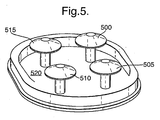
- the four element antenna is shown in Figure 5 and makes use of the same antenna element design as described above with reference to Figure 3 .
- the four element antenna comprises a substantially square arrangement of antenna elements 500-515, mounted on a similar oval shaped saddle plate 520 to that (130) used for the antenna in Figure 1 .
- the antenna elements 500-515 are connected to a similar switching arrangement as that described above with reference to Figure 2 .
- the antenna element 500 is connected to the switch output A, the element 505 to the output B, the element 510 to the output C and the element 515 to the output D.
- the same method may be used to switchably select the antenna elements 500-515 in pairs to generate three sum and difference beams as for the arrangement in the first embodiment above.
- the antenna according to this second embodiment of the present invention has the advantage of being a simpler design. However, the ratio of front-to-back coverage is reduced in comparison to the six element design of Figure 1 , being of the order of only 5dB. This constraint in the performance of the antenna may be of lower significance in systems applied to vehicles or craft other than aircraft.
Landscapes
- Physics & Mathematics (AREA)
- Engineering & Computer Science (AREA)
- Astronomy & Astrophysics (AREA)
- Aviation & Aerospace Engineering (AREA)
- General Physics & Mathematics (AREA)
- Remote Sensing (AREA)
- Variable-Direction Aerials And Aerial Arrays (AREA)
- Support Of Aerials (AREA)
- Details Of Aerials (AREA)
Abstract
Description
- This invention relates to a multi-element antenna and in particular, but not exclusively, to a multi-element antenna and associated switching arrangement designed for use in a monopulse radar collision avoidance system.
- The Traffic alert and Collision Avoidance System (TCAS) is an implementation of the Airborne Collision Avoidance System which is fitted to all aircraft over a certain weight and/or passenger carrying capacity, as mandated by the International Civil Aviation Organisation. A recent implementation of TCAS employs an eight element circular antenna array which is fed through a conventional Butler matrix to generate circular phase modes in the array. The circular modes are phase shifted and combined in a sum/difference hybrid to provide a monopulse radar system with claimed resolution of 2° or better. However, TCAS relies upon the relative phase of two circular modes to detect a potential hazard and as such is sensitive, in certain mounting arrangements, to multipath reflections from parts of a host airframe leading to reduced resolution and potential false alarms.
- Document
US-A1-2002/0036586 describes a switched array, and documentEP-A1-0989629 describes a top-loaded monopole antenna. - From a first aspect the present invention resides in an antenna, comprising a plurality of top-loaded monopole antenna elements mounted above a ground plane for providing coverage over a predetermined range of angles in azimuth using a plurality of beams, each antenna element having a base section and a top section, wherein a feed conductor extends from an entry point provided in the base section to connect to a top element positioned at the top section, and the feed conductor is surrounded by and insulated from a hollow cylindrical electrically conducting stem section that extends from the base section, where the stem section connects to the ground plane, to a level proximate to but separated from the top element, in combination with a switch array, wherein at least some of said plurality of antenna elements are connected to switches in said switch array and wherein said switch array is operable to connect selected pairs of said antenna elements to a signal path to thereby generate each of said plurality of beams and to establish a virtual short circuit in respect of unselected antenna elements.
- Amongst the design constraints for a collision warning/avoidance system suitable for use with military jet aircraft in particular, are good directionality of the beams emitted by the antenna. This is to avoid unwanted emissions, for example in the backward direction relative to the direction of motion of the aircraft, which might interfere with other systems on board or give away the aircraft's presence or position. The antenna and associated switch array according to this first aspect of the present invention, particularly when used to generate sum and difference beams in a monopulse radar based system, offers particularly good directionality in comparison with prior art arrangements.
- The use of top-loaded monopole antenna elements make for a particularly low-profile antenna. Moreover, the design of the antenna feed, in which a feed conductor is surrounded by a hollow cylindrical stem section, enables the input impedance of the antenna element to be set (e.g. to 50 Ohms) by appropriate dimensioning of the inner diameter of the stem section relative to the diameter of the feed conductor, thus forming a quarter-wave transformer. This has the advantage that an external matching transformer for each antenna element is avoided. Furthermore, the inventor in this case has noted that with this antenna element design, in which the top element is effectively fed at the top section of the "stem", there is a slight improvement in the operational bandwidth of the antenna element in comparison with prior art designs.
- Preferably, the match to 50 ohms input impedence is achieved when the antenna is driven in a "sum" mode, that is, when two adjacent antenna elements are driven in phase with equal amplitude.
- Preferably, at least one of the plurality of antenna elements is a passive reflector element connected permanently to ground and positioned so as to increase the directionality of the antenna within the predetermined range of angles.
- In a preferred embodiment, the top element is in the shape of a substantially flat-topped cone.
- Preferably, in the switch array, each of the plurality of switches has a first pole connected to a first antenna element and a second pole connected to a second antenna element and the switch is operable to connect alternately the first or second pole to a signal path and the unconnected pole to ground.
- In a further preferred embodiment, each switch in the switch array is implemented using PIN diodes. In particular, each switch in the switch array is a band-limited shunt multi-throw switch.
- In a further preferred embodiment, the antenna comprises a pentagonal array of five antenna elements clustered around a central sixth element and at least the central sixth element is permanently connected to ground. In order to increase the directionality of the antenna yet further, a further one of the six antenna elements is permanently connected to ground and the remaining four ungrounded antenna elements are connected to the switch array.
- In a yet further preferred embodiment, the antenna comprises a square array of four antenna elements for use with the same switch array.
- The present invention also extends to a collision warning or avoidance system having an antenna, in combination with a switch array, according to preferred embodiments of the present invention outlined above.
- Preferred embodiments of the present invention will now be described by way of example only and with reference to the accompanying drawings, of which:
-
Figure 1 is a perspective view of an antenna according to a preferred embodiment of the present invention; -
Figure 2 shows a switching arrangement suitable for use with the antenna ofFigure 1 , according to a preferred embodiment of the present invention; -
Figure 3 shows a sectional view through a preferred top-loaded monopole antenna element; -
Figure 4 shows a circuit diagram for a preferred switch, based upon PIN diodes; and -
Figure 5 shows an alternative design of antenna according to a further preferred embodiment of the present invention. - Preferred embodiments of the present invention provide an antenna for use in a monopulse radar collision warning/avoidance system and an associated switching arrangement. The antennae and associated switching arrangements are designed for use in a frequency range of interest, preferably 1020-1100MHz (the IFF band). The antennae and switching arrangements are designed for use in particular as part of a collision warning/avoidance system for aircraft, although preferred embodiments of the present invention may also be applied to other types of craft with a requirement for collision warning/avoidance, e.g. road vehicles or ships.
- An antenna according to a first embodiment of the present invention will now be described with reference to
Figure 1 . - Referring to
Figure 1 , the antenna comprises a pentagonal array of fiveantenna elements 100 to 120, surrounding a sixthcentral antenna element 125. The antenna elements 100-125 are mounted on anoval saddle plate 130 which incorporates a ground plane and which enables the antenna to be mounted conveniently on the outer skin of an aircraft fuselage or of another type of vehicle. Aridge 135 is provided around thesaddle plate 130 for attachment of a radome (not shown inFigure 1 ) to cover and protect the array of antenna elements 100-125. Alternatively, or in addition to a radome, the antenna elements 100-125 may be embedded in a dielectric foam or other dielectric material whose dielectric properties may be taken into account in the design of the antenna. - Each of the antenna elements 100-125 is a top-loaded monopole (TLM) antenna, selected in particular to minimise the overall height of the antenna. Preferably, the antenna elements 100-125 are spaced 72mm apart, which is of the order of one quarter-wavelength in the IFF band. Wider element spacing would be desirable, where mounting constraints permit, to help to avoid problems in a feed network arising from the high inter-element coupling. However, space constraints may impose a closer antenna element spacing, of less than one quarter wavelength. In particular, in one application of the present invention, the antenna elements 100-120 are located at points on a radius of 55mm from the
central element 125. Further preferred and advantageous features of the antenna elements 100-125 will be described below. - In order to operate the antenna of this first preferred embodiment of the present invention in a collision warning system, a preferred switching arrangement and method of operation of the switches will now be described with reference to
Figure 2 and further with reference toFigure 1 . - Referring to
Figure 2 , a switching arrangement is shown comprisingswitches Figure 2 , to one of twosignal paths signal paths conventional hybrid coupler 225 for coupling sum anddifference signal paths Figure 2 ). - The switch outputs are linked to four of the antenna elements 100-125 of the antenna so that only those four antenna elements are used actively to transmit or receive signals, the remaining two elements being short-circuited permanently to the ground plane so that they act as passive reflector elements. This has the advantage that the level of back-facing coverage of the antenna is reduced in comparison with the level of generally forward-facing coverage, with respect to the direction of flight of the aircraft carrying the antenna. In practice, a front-to-back ratio of up to 13dB has been achieved in the coverage with this design.
- Preferably the switch output A is connected to the
antenna element 100; the switch output B is connected to theantenna element 105; the switch output C is connected to theantenna element 110; and the switch output D is connected to theantenna element 115. Within the switching arrangement, switch 205 (S1) is operable to connect either antenna element 105 (output B) or antenna element 115 (output D) to theinput signal path 215, whileswitch 210 is operable to connect either antenna element 100 (output A) or antenna element 110 (output C) toinput signal path 220. Thus, antenna elements 100-115 may be selected in pairs, each pair providing substantially identically-shaped sum and difference beam patterns in three different predetermined directions in azimuth - beam direction being defined in this case as the azimuth of the null in the difference pattern generated by the selected pair of antenna elements - with an appropriate choice of switch positions for switches S1 and S2, as summarised in the following table. In this table, "X" indicates that the switch output and hence the respective antenna element is connected to a signal path, while "-" indicates that the switch output and hence the respective antenna element is shorted to Ground.S1 S2 Output A (Element 100) Output B (Element 105) Output C (Element 110) Output D (Element 115) Beam Direction 0 0 Not Used 0 1 - - X X +72° 1 0 X X - - -72° 1 1 - X X - 0° - Each unselected pair of switch outputs are preferably shorted to ground in the switch and the signal path lengths between the switch output and the respective antenna elements are carefully chosen - a multiple of half-wavelengths of the operational signals - to ensure that there is a virtual short circuit present at the unselected antenna elements at each switch combination. The unselected elements therefore act as passive reflectors, so improving the directionality of the beams produced by the corresponding selected pair of antenna elements. In this table, it is assumed that a beam direction of 0° represents a directly forward-facing beam with respect to the host aircraft. In practice, the antenna according to the first embodiment of the present invention provides a total angular coverage in azimuth of at least ±120°.
- Preferably,
antenna elements position 0, as thegrounded antenna elements - As mentioned above, in order to provide the correct reactive load to the antenna elements not selected in a particular switch combination, the lengths of transmission line which connect the antenna elements to the switches must be of the correct length. In particular, where the
transmission line stubs 240 within the switching arrangement shown inFigure 2 represent the entire length of transmission line connecting the switch S1 or S2 to a respective antenna element, the path lengths are equalised and set in length to be a multiple of half-wavelengths of the operational signals. Furthermore, to maintain the correct reactance over a desired frequency band, preferably over the frequency range 1020-1100MHz, the transmission line lengths between antenna element and switch must be as short as possible, preferably achieved by locating the switching arrangement as close as possible to the antenna. - A preferred design for an antenna element 100-125 will now be described with reference to
Figure 3 . - Referring to
Figure 3 , a sectional view is provided through a top-loadedmonopole antenna element 300. Theantenna element 300 is shown comprising a hollow cylindricalmetal stem section 305 extending from abase section 310 of the element, thestem section 305 having an electrically conductingfeed 315 disposed within it, separated from the inner wall of thestem section 305 by anair gap 320, the feed also extending from within thebase section 310 to connect to a flat or, preferably, a conical circular top "plate"element 325, approximately 2mm thick. Thestem section 305 extends to a height of approximately 32mm above thesaddle plate 130. A dielectric "plug" 330 of low dielectric constant (εr=2) is inserted into the air gap at the open end of thestem section 305 below thetop element 325 to maintain a separation between thefeed 315 and the inner wall of thestem section 305, and to add sturdiness to theantenna element 300. - A
coaxial connector 335 extends through thebase section 310 of theantenna element 300 to provide an electrical connection to thefeed 315 by means of a conventionalcoaxial socket 337. Thebase section 310 of theantenna element 300 is inserted into a hole through thesaddle plate 130 from below and secured. - Preferably, the
top element 325 comprises a centralflat section 340 surrounded by aconical skirt section 345 inclined at approximately 30° below the plane of theflat section 340. This has the advantage over use of an entirely flat top element that the outer antenna elements 100-120 enable a closer-fitting and hence smaller radome to be provided, minimising the overall height and width of the antenna structure. - Preferably the radius of the
top element 325 is selected to tune the antenna to substantially the centre frequency in the frequency band of interest, e.g. the IFF band. Preferably, for the IFF band, the radius of thetop element 325 is approximately 20mm. Furthermore, the dimensions of thestem section 305, in particular the radius of the inner and outer conductors of the coaxial transformer formed inside thestem section 325, are selected to ensure that the input impedance of theantenna element 300 of 50 ohms when twoadjacent antenna elements 300 are driven in phase with equal amplitude. i.e. in the "sum" mode. However, while a good impedance match is achieved in the "sum" mode, a compromise may be required as regards impedance matching in the "difference" mode, i.e. when twoadjacent antenna elements 300 are driven in antiphase preferably, the mismatch in the "difference" mode is compensated for by addingmatching elements 245, e.g. a matching transformer and matching stubs, in the difference path following thehybrid coupler 225. If preferred, theair gap 320, which is typically only 1 or 2mm wide, may be filled with a dielectric material of an appropriate dielectric constant, preferably of εr=2. - Whereas the switching arrangement described functionally above with reference to
Figure 2 may be implemented in one of a number of conventional ways, a preferred implementation of the switching arrangement shown functionally inFigure 2 will now be described with reference toFigure 4 . - Referring to
Figure 4 , a circuit diagram is shown for a conventional band-limited shunt multi-throw switch. Two of these switches are required to implement the switching arrangement shown inFigure 2 , one for each of the switches S1 and S2. A common radio frequency (RF)input 405 to the switch would be connected to asignal path Figure 2 . TheRF input 405 leads to a T-junction 410 where the signal path divides into two separate switchable branches, one branch leading to afirst RF output 415 and the other branch to asecond RF output 420. Each switchable branch comprises a pair of cascaded quarter-wavelength sections oftransmission line 425, each terminated by a shunt PIN (p-type, intrinsic, n-type)diode 430, connected between the end of the respective quarter-wavelength section oftransmission line 425 and the ground. - When the switch is in one of its two possible states, the
diodes 430 are forward biased in one branch of the switch and reverse biased in the other. The biasing is applied by means ofrespective bias inputs diodes 430 that are forward biased connect the respectivetransmission line sections 425 to ground, so forming a quarter wavelength stub with a high impedance. Thosediodes 430 that are reverse biased appear effectively as small (unwanted) capacitances. An input (405) RF signal is able to travel along that branch of the switch having the reversedbiased diodes 430 to therespective RF output - Each of the first and second RF outputs 415, 420 is connected to a different antenna element, for example in the configuration described above with reference to
Figure 1 and Figure 2 . As mentioned above with reference toFigure 2 , it is important that a virtual short circuit exists at the points of connection to unselected antenna elements in any given switch setting. This is achieved by ensuring that the path lengths between for example the T-junction 410 in the switch and the respective antenna elements are set to be a multiple of half wavelengths of the operational signals. - In a second preferred embodiment of the present invention, a simpler four element antenna is provided, using the same switching arrangement as used in the first embodiment and as described with reference to
Figure 2 . The four element antenna is shown inFigure 5 and makes use of the same antenna element design as described above with reference toFigure 3 . - Referring to
Figure 5 , the four element antenna comprises a substantially square arrangement of antenna elements 500-515, mounted on a similar oval shapedsaddle plate 520 to that (130) used for the antenna inFigure 1 . The antenna elements 500-515 are connected to a similar switching arrangement as that described above with reference toFigure 2 . In particular, theantenna element 500 is connected to the switch output A, theelement 505 to the output B, theelement 510 to the output C and theelement 515 to the output D. Thus the same method may be used to switchably select the antenna elements 500-515 in pairs to generate three sum and difference beams as for the arrangement in the first embodiment above. - The antenna according to this second embodiment of the present invention has the advantage of being a simpler design. However, the ratio of front-to-back coverage is reduced in comparison to the six element design of
Figure 1 , being of the order of only 5dB. This constraint in the performance of the antenna may be of lower significance in systems applied to vehicles or craft other than aircraft.
Claims (14)
- An antenna, comprising a plurality of antenna elements (100,105,...,125) mounted above a ground plane (130) for providing coverage over a predetermined range of angles in azimuth using a plurality of beams, in combination with a switch array, wherein at least some of said plurality of antenna elements (100,105...,125) are connected to switches (S1,S2) in said switch array and wherein said switch array is operable to connect selected pairs of said antenna elements to a signal path to thereby generate each of said plurality of beams and to establish a virtual short circuit in respect of unselected antenna elements, characterized in each antenna element (100,105,...,125) being a top-loaded monopole antenna element (300) having a base section (310) and a top section, wherein a feed conductor (315) extends from an entry point provided in the base section (310) to connect to a top element (325) positioned at the top section, and the feed conductor (315) is surrounded by and insulated from a hollow cylindrical electrically conducting stem section (305) that extends from the base section (310), where the stem section (305) connects to the ground plane (130), to a level proximate to but separated from the top element (325).
- An antenna according to Claim 1, wherein at least one of said plurality of antenna elements (100,105,...,125) is a passive reflector element connected permanently to ground (130) and positioned so as to increase the directionality of the antenna within said predetermined range of angles.
- An antenna according to Claim 1 or Claim 2, wherein the top element (325) is in the shape of a substantially flat-topped cone.
- An antenna according to any one of claims 1 to 3, wherein the ratio of the inner diameter of the stem section (305) to the diameter of the feed conductor (315) is selected to ensure that the input impedance of the antenna element is substantially 50 ohms.
- An antenna according to any one of the preceding claims, wherein each of said plurality of switches (S1,S2) has a first pole (415) connected to a first antenna element and a second pole (420) connected to a second antenna element and wherein the switch is operable to connect alternately the first or second pole to a signal path (405) and the unconnected pole to ground.
- An antenna according to any one of the preceding claims, wherein each switch (S1,S2) in said switch array is implemented using PIN diodes.
- An antenna according to Claim 6, wherein each switch (S1,S2) in said switch array is a band-limited shunt multi-throw switch.
- An antenna according to any one of the preceding claims, wherein said antenna comprises a pentagonal array of five antenna elements (100,105,...,120) clustered around a central sixth element (125) and wherein at least said central sixth element (125) is a passive reflector element permanently connected to ground.
- An antenna according to Claim 8, wherein a further one of said six antenna elements is permanently connected to ground and wherein the remaining four ungrounded elements (100,105,110,115) are connected to said switch array.
- An antenna according to any one of claims 1 to 7, wherein said antenna comprises a substantially square array of four antenna elements (500,505,510,515) and each of said four antenna elements is connected to a switch in said switch array.
- An antenna according to any one of the preceding claims, wherein said multiple beams are sum and difference beams in a monopulse radar system.
- An antenna according to any one of the preceding claims, wherein said antenna elements (100,105,...,125) are embedded within a dielectric foam material.
- An antenna according to any one of the preceding claims, further comprising a radome to cover said antenna elements.
- A collision warning or avoidance system having an antenna in combination with a switch array according to any one of claims 1 to 13.
Priority Applications (1)
| Application Number | Priority Date | Filing Date | Title |
|---|---|---|---|
| EP07824937A EP2095462B1 (en) | 2006-12-21 | 2007-11-29 | Antenna |
Applications Claiming Priority (5)
| Application Number | Priority Date | Filing Date | Title |
|---|---|---|---|
| GB0625557A GB0625557D0 (en) | 2006-12-21 | 2006-12-21 | Antenna |
| GB0625564A GB0625564D0 (en) | 2006-12-21 | 2006-12-21 | Antenna |
| EP06256461 | 2006-12-21 | ||
| EP07824937A EP2095462B1 (en) | 2006-12-21 | 2007-11-29 | Antenna |
| PCT/GB2007/050727 WO2008075093A1 (en) | 2006-12-21 | 2007-11-29 | Antenna |
Publications (2)
| Publication Number | Publication Date |
|---|---|
| EP2095462A1 EP2095462A1 (en) | 2009-09-02 |
| EP2095462B1 true EP2095462B1 (en) | 2010-07-14 |
Family
ID=39066767
Family Applications (1)
| Application Number | Title | Priority Date | Filing Date |
|---|---|---|---|
| EP07824937A Not-in-force EP2095462B1 (en) | 2006-12-21 | 2007-11-29 | Antenna |
Country Status (7)
| Country | Link |
|---|---|
| US (1) | US7868818B2 (en) |
| EP (1) | EP2095462B1 (en) |
| AT (1) | ATE474343T1 (en) |
| AU (1) | AU2007335952B2 (en) |
| DE (1) | DE602007007814D1 (en) |
| ES (1) | ES2347838T3 (en) |
| WO (1) | WO2008075093A1 (en) |
Cited By (1)
| Publication number | Priority date | Publication date | Assignee | Title |
|---|---|---|---|---|
| CN102253382A (en) * | 2011-05-31 | 2011-11-23 | 中国航空无线电电子研究所 | Digital intermediate frequency single pulse orientation method |
Families Citing this family (14)
| Publication number | Priority date | Publication date | Assignee | Title |
|---|---|---|---|---|
| CA2763850A1 (en) * | 2009-06-09 | 2010-12-16 | The Secretary Of State For Defence | An electrically small ultra-wideband antenna for mobile handsets and computer networks |
| US8269684B2 (en) * | 2010-06-08 | 2012-09-18 | Sensor Systems, Inc. | Navigation, identification, and collision avoidance antenna systems |
| US8838036B2 (en) * | 2011-09-19 | 2014-09-16 | Broadcom Corporation | Switch for transmit/receive mode selection and antenna polarization diversity |
| US9016631B2 (en) | 2012-04-09 | 2015-04-28 | R4 Integration, Inc. | Multi-purpose hatch system |
| USD697900S1 (en) * | 2012-07-18 | 2014-01-21 | Kmw Inc. | Antenna radome |
| US8798670B2 (en) * | 2012-08-03 | 2014-08-05 | Blackberry Limited | Mobile wireless communications device with DDPDT RF switch and related methods |
| WO2015108435A1 (en) * | 2014-01-16 | 2015-07-23 | Llc "Topcon Positioning Systems" | Gnss base station antenna system with reduced sensitivity to reflections from nearby objects |
| US10074909B2 (en) | 2015-07-21 | 2018-09-11 | Laird Technologies, Inc. | Omnidirectional single-input single-output multiband/broadband antennas |
| CN206657857U (en) * | 2017-04-13 | 2017-11-21 | 智邦科技股份有限公司 | Antenna module |
| US10290930B2 (en) * | 2017-07-18 | 2019-05-14 | Honeywell International Inc. | Crossed dipole with enhanced gain at low elevation |
| CN109167185B (en) * | 2018-08-27 | 2021-01-15 | 京信通信技术(广州)有限公司 | Beam switchable antenna |
| US11476577B2 (en) * | 2019-06-18 | 2022-10-18 | University Of Massachusetts | Ultrawideband parallel plate lens multi-beamformer apparatus and method |
| US20230231307A1 (en) * | 2022-01-14 | 2023-07-20 | Mediatek Inc. | Antenna |
| CN115513665B (en) * | 2022-10-28 | 2025-08-19 | 中信科移动通信技术股份有限公司 | Phase shifter and base station antenna |
Family Cites Families (23)
| Publication number | Priority date | Publication date | Assignee | Title |
|---|---|---|---|---|
| US3334348A (en) * | 1966-11-25 | 1967-08-01 | Granger Associates | Steerable monopole antenna system having a plurality of reflectors, said reflectors comprising a series of tubular vacuum switches |
| US3419873A (en) * | 1964-12-09 | 1968-12-31 | Control Data Corp | Monopole antenna |
| US3380061A (en) * | 1965-03-04 | 1968-04-23 | Control Data Corp | Top loaded monopole antenna with guy wire line tightener |
| US3384896A (en) * | 1965-06-28 | 1968-05-21 | Northrop Corp | Vertical monopole with spiral-shaped top loading |
| US3484787A (en) * | 1967-06-12 | 1969-12-16 | Itt | Folded monopole antenna with top loading and lumped inductance at bottom |
| US4313121A (en) * | 1980-03-13 | 1982-01-26 | The United States Of America As Represented By The Secretary Of The Army | Compact monopole antenna with structured top load |
| US4466003A (en) * | 1982-02-09 | 1984-08-14 | The United States Of America As Represented By The Secretary Of The Navy | Compact wideband multiple conductor monopole antenna |
| CA1239223A (en) * | 1984-07-02 | 1988-07-12 | Robert Milne | Adaptive array antenna |
| US4939525A (en) * | 1988-03-31 | 1990-07-03 | Cincinnati Electronics Corporation | Tunable short monopole top-loaded antenna |
| US4897664A (en) * | 1988-06-03 | 1990-01-30 | General Dynamics Corp., Pomona Division | Image plate/short backfire antenna |
| US5191349A (en) * | 1990-08-08 | 1993-03-02 | Honeywell Inc. | Apparatus and method for an amplitude monopulse directional antenna |
| US5479176A (en) | 1994-10-21 | 1995-12-26 | Metricom, Inc. | Multiple-element driven array antenna and phasing method |
| US5767807A (en) * | 1996-06-05 | 1998-06-16 | International Business Machines Corporation | Communication system and methods utilizing a reactively controlled directive array |
| JP2000077923A (en) | 1998-09-01 | 2000-03-14 | Nippon Antenna Co Ltd | Automotive antenna |
| US6452565B1 (en) | 1999-10-29 | 2002-09-17 | Antenova Limited | Steerable-beam multiple-feed dielectric resonator antenna |
| JP2001345633A (en) | 2000-03-28 | 2001-12-14 | Matsushita Electric Ind Co Ltd | Antenna device |
| US20020036586A1 (en) * | 2000-09-22 | 2002-03-28 | Tantivy Communications, Inc. | Adaptive antenna for use in wireless communication systems |
| JP2003258533A (en) | 2002-02-28 | 2003-09-12 | Tsutomu Yoneyama | Directivity switching antenna |
| US6987493B2 (en) * | 2002-04-15 | 2006-01-17 | Paratek Microwave, Inc. | Electronically steerable passive array antenna |
| US6917341B2 (en) * | 2002-06-11 | 2005-07-12 | Matsushita Electric Industrial Co., Ltd. | Top-loading monopole antenna apparatus with short-circuit conductor connected between top-loading electrode and grounding conductor |
| DE10304909B4 (en) * | 2003-02-06 | 2014-10-09 | Heinz Lindenmeier | Antenna with monopoly character for several radio services |
| US6859181B2 (en) * | 2003-06-24 | 2005-02-22 | General Motors Corporation | Integrated spiral and top-loaded monopole antenna |
| US7265727B2 (en) * | 2005-06-03 | 2007-09-04 | Raytheon Company | Top loaded disk monopole antenna |
-
2007
- 2007-11-29 US US12/067,123 patent/US7868818B2/en not_active Expired - Fee Related
- 2007-11-29 ES ES07824937T patent/ES2347838T3/en active Active
- 2007-11-29 EP EP07824937A patent/EP2095462B1/en not_active Not-in-force
- 2007-11-29 AU AU2007335952A patent/AU2007335952B2/en not_active Ceased
- 2007-11-29 WO PCT/GB2007/050727 patent/WO2008075093A1/en not_active Ceased
- 2007-11-29 DE DE602007007814T patent/DE602007007814D1/en active Active
- 2007-11-29 AT AT07824937T patent/ATE474343T1/en not_active IP Right Cessation
Cited By (2)
| Publication number | Priority date | Publication date | Assignee | Title |
|---|---|---|---|---|
| CN102253382A (en) * | 2011-05-31 | 2011-11-23 | 中国航空无线电电子研究所 | Digital intermediate frequency single pulse orientation method |
| CN102253382B (en) * | 2011-05-31 | 2012-10-03 | 中国航空无线电电子研究所 | Digital intermediate frequency single pulse orientation method |
Also Published As
| Publication number | Publication date |
|---|---|
| US7868818B2 (en) | 2011-01-11 |
| US20100060513A1 (en) | 2010-03-11 |
| DE602007007814D1 (en) | 2010-08-26 |
| ATE474343T1 (en) | 2010-07-15 |
| WO2008075093A1 (en) | 2008-06-26 |
| EP2095462A1 (en) | 2009-09-02 |
| AU2007335952A1 (en) | 2008-06-26 |
| ES2347838T3 (en) | 2010-11-04 |
| AU2007335952B2 (en) | 2011-11-24 |
Similar Documents
| Publication | Publication Date | Title |
|---|---|---|
| US7868818B2 (en) | Multi-element antenna | |
| US5650792A (en) | Combination GPS and VHF antenna | |
| US6795021B2 (en) | Tunable multi-band antenna array | |
| US9825373B1 (en) | Monopatch antenna | |
| AU2001255820B2 (en) | Nested turnstile antenna | |
| US6618016B1 (en) | Eight-element anti-jam aircraft GPS antennas | |
| EP0434282B1 (en) | Dual mode antenna apparatus having slotted waveguide and broadband arrays | |
| US4812855A (en) | Dipole antenna with parasitic elements | |
| US11228108B2 (en) | Multiband circularly polarised antenna | |
| US20190067822A1 (en) | Waveguide feed network architecture for wideband, low profile, dual polarized planar horn array antennas | |
| CN101103491A (en) | Linearly polarized antenna and radar equipment using the same | |
| US7385560B1 (en) | Aircraft directional/omnidirectional antenna arrangement | |
| EP1905126B1 (en) | Leaky wave antenna with radiating structure including fractal loops | |
| US6307510B1 (en) | Patch dipole array antenna and associated methods | |
| US7907098B1 (en) | Log periodic antenna | |
| US9214729B2 (en) | Antenna and array antenna | |
| US9013360B1 (en) | Continuous band antenna (CBA) with switchable quadrant beams and selectable polarization | |
| CN115395213B (en) | Antenna unit, array antenna, radar sensor and electronic equipment | |
| CN109116310B (en) | A secondary radar radio frequency transceiver for aircraft anti-collision system | |
| JPH03213005A (en) | Forced excitation array antenna | |
| Sadhukhan et al. | Compact S-band ship borne reconfigurable receiving antenna for down-range telemetry application | |
| JP2997321B2 (en) | Aircraft antenna with corning and banking correction functions | |
| US12620709B2 (en) | Full-duplex circular parasitic array assembly | |
| US6181277B1 (en) | Microstrip antenna | |
| US12176631B1 (en) | Electrically small wideband resonant loop antenna systems and methods |
Legal Events
| Date | Code | Title | Description |
|---|---|---|---|
| PUAI | Public reference made under article 153(3) epc to a published international application that has entered the european phase |
Free format text: ORIGINAL CODE: 0009012 |
|
| 17P | Request for examination filed |
Effective date: 20090618 |
|
| AK | Designated contracting states |
Kind code of ref document: A1 Designated state(s): AT BE BG CH CY CZ DE DK EE ES FI FR GB GR HU IE IS IT LI LT LU LV MC MT NL PL PT RO SE SI SK TR |
|
| GRAP | Despatch of communication of intention to grant a patent |
Free format text: ORIGINAL CODE: EPIDOSNIGR1 |
|
| DAX | Request for extension of the european patent (deleted) | ||
| GRAS | Grant fee paid |
Free format text: ORIGINAL CODE: EPIDOSNIGR3 |
|
| GRAA | (expected) grant |
Free format text: ORIGINAL CODE: 0009210 |
|
| AK | Designated contracting states |
Kind code of ref document: B1 Designated state(s): AT BE BG CH CY CZ DE DK EE ES FI FR GB GR HU IE IS IT LI LT LU LV MC MT NL PL PT RO SE SI SK TR |
|
| REG | Reference to a national code |
Ref country code: GB Ref legal event code: FG4D |
|
| REG | Reference to a national code |
Ref country code: CH Ref legal event code: EP |
|
| REG | Reference to a national code |
Ref country code: IE Ref legal event code: FG4D |
|
| REF | Corresponds to: |
Ref document number: 602007007814 Country of ref document: DE Date of ref document: 20100826 Kind code of ref document: P |
|
| REG | Reference to a national code |
Ref country code: SE Ref legal event code: TRGR |
|
| REG | Reference to a national code |
Ref country code: ES Ref legal event code: FG2A Ref document number: 2347838 Country of ref document: ES Kind code of ref document: T3 |
|
| REG | Reference to a national code |
Ref country code: NL Ref legal event code: VDEP Effective date: 20100714 |
|
| LTIE | Lt: invalidation of european patent or patent extension |
Effective date: 20100714 |
|
| PG25 | Lapsed in a contracting state [announced via postgrant information from national office to epo] |
Ref country code: FI Free format text: LAPSE BECAUSE OF FAILURE TO SUBMIT A TRANSLATION OF THE DESCRIPTION OR TO PAY THE FEE WITHIN THE PRESCRIBED TIME-LIMIT Effective date: 20100714 Ref country code: AT Free format text: LAPSE BECAUSE OF FAILURE TO SUBMIT A TRANSLATION OF THE DESCRIPTION OR TO PAY THE FEE WITHIN THE PRESCRIBED TIME-LIMIT Effective date: 20100714 Ref country code: NL Free format text: LAPSE BECAUSE OF FAILURE TO SUBMIT A TRANSLATION OF THE DESCRIPTION OR TO PAY THE FEE WITHIN THE PRESCRIBED TIME-LIMIT Effective date: 20100714 Ref country code: LT Free format text: LAPSE BECAUSE OF FAILURE TO SUBMIT A TRANSLATION OF THE DESCRIPTION OR TO PAY THE FEE WITHIN THE PRESCRIBED TIME-LIMIT Effective date: 20100714 |
|
| PG25 | Lapsed in a contracting state [announced via postgrant information from national office to epo] |
Ref country code: PT Free format text: LAPSE BECAUSE OF FAILURE TO SUBMIT A TRANSLATION OF THE DESCRIPTION OR TO PAY THE FEE WITHIN THE PRESCRIBED TIME-LIMIT Effective date: 20101115 Ref country code: PL Free format text: LAPSE BECAUSE OF FAILURE TO SUBMIT A TRANSLATION OF THE DESCRIPTION OR TO PAY THE FEE WITHIN THE PRESCRIBED TIME-LIMIT Effective date: 20100714 Ref country code: SI Free format text: LAPSE BECAUSE OF FAILURE TO SUBMIT A TRANSLATION OF THE DESCRIPTION OR TO PAY THE FEE WITHIN THE PRESCRIBED TIME-LIMIT Effective date: 20100714 Ref country code: IS Free format text: LAPSE BECAUSE OF FAILURE TO SUBMIT A TRANSLATION OF THE DESCRIPTION OR TO PAY THE FEE WITHIN THE PRESCRIBED TIME-LIMIT Effective date: 20101114 Ref country code: BG Free format text: LAPSE BECAUSE OF FAILURE TO SUBMIT A TRANSLATION OF THE DESCRIPTION OR TO PAY THE FEE WITHIN THE PRESCRIBED TIME-LIMIT Effective date: 20101014 Ref country code: CY Free format text: LAPSE BECAUSE OF FAILURE TO SUBMIT A TRANSLATION OF THE DESCRIPTION OR TO PAY THE FEE WITHIN THE PRESCRIBED TIME-LIMIT Effective date: 20100714 |
|
| PG25 | Lapsed in a contracting state [announced via postgrant information from national office to epo] |
Ref country code: GR Free format text: LAPSE BECAUSE OF FAILURE TO SUBMIT A TRANSLATION OF THE DESCRIPTION OR TO PAY THE FEE WITHIN THE PRESCRIBED TIME-LIMIT Effective date: 20101015 Ref country code: LV Free format text: LAPSE BECAUSE OF FAILURE TO SUBMIT A TRANSLATION OF THE DESCRIPTION OR TO PAY THE FEE WITHIN THE PRESCRIBED TIME-LIMIT Effective date: 20100714 Ref country code: BE Free format text: LAPSE BECAUSE OF FAILURE TO SUBMIT A TRANSLATION OF THE DESCRIPTION OR TO PAY THE FEE WITHIN THE PRESCRIBED TIME-LIMIT Effective date: 20100714 |
|
| PG25 | Lapsed in a contracting state [announced via postgrant information from national office to epo] |
Ref country code: DK Free format text: LAPSE BECAUSE OF FAILURE TO SUBMIT A TRANSLATION OF THE DESCRIPTION OR TO PAY THE FEE WITHIN THE PRESCRIBED TIME-LIMIT Effective date: 20100714 |
|
| PLBE | No opposition filed within time limit |
Free format text: ORIGINAL CODE: 0009261 |
|
| STAA | Information on the status of an ep patent application or granted ep patent |
Free format text: STATUS: NO OPPOSITION FILED WITHIN TIME LIMIT |
|
| PG25 | Lapsed in a contracting state [announced via postgrant information from national office to epo] |
Ref country code: EE Free format text: LAPSE BECAUSE OF FAILURE TO SUBMIT A TRANSLATION OF THE DESCRIPTION OR TO PAY THE FEE WITHIN THE PRESCRIBED TIME-LIMIT Effective date: 20100714 Ref country code: SK Free format text: LAPSE BECAUSE OF FAILURE TO SUBMIT A TRANSLATION OF THE DESCRIPTION OR TO PAY THE FEE WITHIN THE PRESCRIBED TIME-LIMIT Effective date: 20100714 Ref country code: CZ Free format text: LAPSE BECAUSE OF FAILURE TO SUBMIT A TRANSLATION OF THE DESCRIPTION OR TO PAY THE FEE WITHIN THE PRESCRIBED TIME-LIMIT Effective date: 20100714 Ref country code: RO Free format text: LAPSE BECAUSE OF FAILURE TO SUBMIT A TRANSLATION OF THE DESCRIPTION OR TO PAY THE FEE WITHIN THE PRESCRIBED TIME-LIMIT Effective date: 20100714 |
|
| 26N | No opposition filed |
Effective date: 20110415 |
|
| PG25 | Lapsed in a contracting state [announced via postgrant information from national office to epo] |
Ref country code: MC Free format text: LAPSE BECAUSE OF NON-PAYMENT OF DUE FEES Effective date: 20101130 |
|
| REG | Reference to a national code |
Ref country code: DE Ref legal event code: R097 Ref document number: 602007007814 Country of ref document: DE Effective date: 20110415 |
|
| PG25 | Lapsed in a contracting state [announced via postgrant information from national office to epo] |
Ref country code: IE Free format text: LAPSE BECAUSE OF NON-PAYMENT OF DUE FEES Effective date: 20101129 |
|
| PG25 | Lapsed in a contracting state [announced via postgrant information from national office to epo] |
Ref country code: IT Free format text: LAPSE BECAUSE OF NON-PAYMENT OF DUE FEES Effective date: 20101129 Ref country code: MT Free format text: LAPSE BECAUSE OF FAILURE TO SUBMIT A TRANSLATION OF THE DESCRIPTION OR TO PAY THE FEE WITHIN THE PRESCRIBED TIME-LIMIT Effective date: 20100714 |
|
| REG | Reference to a national code |
Ref country code: CH Ref legal event code: PL |
|
| PG25 | Lapsed in a contracting state [announced via postgrant information from national office to epo] |
Ref country code: CH Free format text: LAPSE BECAUSE OF NON-PAYMENT OF DUE FEES Effective date: 20111130 Ref country code: LI Free format text: LAPSE BECAUSE OF NON-PAYMENT OF DUE FEES Effective date: 20111130 |
|
| PG25 | Lapsed in a contracting state [announced via postgrant information from national office to epo] |
Ref country code: HU Free format text: LAPSE BECAUSE OF FAILURE TO SUBMIT A TRANSLATION OF THE DESCRIPTION OR TO PAY THE FEE WITHIN THE PRESCRIBED TIME-LIMIT Effective date: 20110115 Ref country code: LU Free format text: LAPSE BECAUSE OF NON-PAYMENT OF DUE FEES Effective date: 20101129 |
|
| PG25 | Lapsed in a contracting state [announced via postgrant information from national office to epo] |
Ref country code: TR Free format text: LAPSE BECAUSE OF FAILURE TO SUBMIT A TRANSLATION OF THE DESCRIPTION OR TO PAY THE FEE WITHIN THE PRESCRIBED TIME-LIMIT Effective date: 20100714 |
|
| REG | Reference to a national code |
Ref country code: FR Ref legal event code: PLFP Year of fee payment: 9 |
|
| REG | Reference to a national code |
Ref country code: FR Ref legal event code: PLFP Year of fee payment: 10 |
|
| REG | Reference to a national code |
Ref country code: FR Ref legal event code: PLFP Year of fee payment: 11 |
|
| PGFP | Annual fee paid to national office [announced via postgrant information from national office to epo] |
Ref country code: SE Payment date: 20181126 Year of fee payment: 12 |
|
| PGFP | Annual fee paid to national office [announced via postgrant information from national office to epo] |
Ref country code: ES Payment date: 20181218 Year of fee payment: 12 Ref country code: FR Payment date: 20181127 Year of fee payment: 12 Ref country code: IT Payment date: 20181122 Year of fee payment: 12 Ref country code: GB Payment date: 20181130 Year of fee payment: 12 |
|
| PGFP | Annual fee paid to national office [announced via postgrant information from national office to epo] |
Ref country code: DE Payment date: 20190131 Year of fee payment: 12 |
|
| REG | Reference to a national code |
Ref country code: DE Ref legal event code: R119 Ref document number: 602007007814 Country of ref document: DE |
|
| REG | Reference to a national code |
Ref country code: SE Ref legal event code: EUG |
|
| PG25 | Lapsed in a contracting state [announced via postgrant information from national office to epo] |
Ref country code: SE Free format text: LAPSE BECAUSE OF NON-PAYMENT OF DUE FEES Effective date: 20191130 |
|
| GBPC | Gb: european patent ceased through non-payment of renewal fee |
Effective date: 20191129 |
|
| PG25 | Lapsed in a contracting state [announced via postgrant information from national office to epo] |
Ref country code: DE Free format text: LAPSE BECAUSE OF NON-PAYMENT OF DUE FEES Effective date: 20200603 Ref country code: GB Free format text: LAPSE BECAUSE OF NON-PAYMENT OF DUE FEES Effective date: 20191129 Ref country code: IT Free format text: LAPSE BECAUSE OF NON-PAYMENT OF DUE FEES Effective date: 20191129 |
|
| REG | Reference to a national code |
Ref country code: ES Ref legal event code: FD2A Effective date: 20210601 |
|
| PG25 | Lapsed in a contracting state [announced via postgrant information from national office to epo] |
Ref country code: FR Free format text: LAPSE BECAUSE OF NON-PAYMENT OF DUE FEES Effective date: 20191202 |
|
| PG25 | Lapsed in a contracting state [announced via postgrant information from national office to epo] |
Ref country code: ES Free format text: LAPSE BECAUSE OF NON-PAYMENT OF DUE FEES Effective date: 20191130 |